EP1942531A2 - Dispositif électroluminescent et illuminateur l'utilisant - Google Patents
Dispositif électroluminescent et illuminateur l'utilisant Download PDFInfo
- Publication number
- EP1942531A2 EP1942531A2 EP08002195A EP08002195A EP1942531A2 EP 1942531 A2 EP1942531 A2 EP 1942531A2 EP 08002195 A EP08002195 A EP 08002195A EP 08002195 A EP08002195 A EP 08002195A EP 1942531 A2 EP1942531 A2 EP 1942531A2
- Authority
- EP
- European Patent Office
- Prior art keywords
- light
- phosphor
- light emitting
- emitting device
- light emitter
- Prior art date
- Legal status (The legal status is an assumption and is not a legal conclusion. Google has not performed a legal analysis and makes no representation as to the accuracy of the status listed.)
- Granted
Links
Images


Classifications
-
- C—CHEMISTRY; METALLURGY
- C09—DYES; PAINTS; POLISHES; NATURAL RESINS; ADHESIVES; COMPOSITIONS NOT OTHERWISE PROVIDED FOR; APPLICATIONS OF MATERIALS NOT OTHERWISE PROVIDED FOR
- C09K—MATERIALS FOR MISCELLANEOUS APPLICATIONS, NOT PROVIDED FOR ELSEWHERE
- C09K11/00—Luminescent, e.g. electroluminescent, chemiluminescent materials
- C09K11/08—Luminescent, e.g. electroluminescent, chemiluminescent materials containing inorganic luminescent materials
- C09K11/77—Luminescent, e.g. electroluminescent, chemiluminescent materials containing inorganic luminescent materials containing rare earth metals
- C09K11/7728—Luminescent, e.g. electroluminescent, chemiluminescent materials containing inorganic luminescent materials containing rare earth metals containing europium
- C09K11/7734—Aluminates
-
- C—CHEMISTRY; METALLURGY
- C09—DYES; PAINTS; POLISHES; NATURAL RESINS; ADHESIVES; COMPOSITIONS NOT OTHERWISE PROVIDED FOR; APPLICATIONS OF MATERIALS NOT OTHERWISE PROVIDED FOR
- C09K—MATERIALS FOR MISCELLANEOUS APPLICATIONS, NOT PROVIDED FOR ELSEWHERE
- C09K11/00—Luminescent, e.g. electroluminescent, chemiluminescent materials
- C09K11/08—Luminescent, e.g. electroluminescent, chemiluminescent materials containing inorganic luminescent materials
- C09K11/77—Luminescent, e.g. electroluminescent, chemiluminescent materials containing inorganic luminescent materials containing rare earth metals
- C09K11/7728—Luminescent, e.g. electroluminescent, chemiluminescent materials containing inorganic luminescent materials containing rare earth metals containing europium
- C09K11/77342—Silicates
-
- C—CHEMISTRY; METALLURGY
- C09—DYES; PAINTS; POLISHES; NATURAL RESINS; ADHESIVES; COMPOSITIONS NOT OTHERWISE PROVIDED FOR; APPLICATIONS OF MATERIALS NOT OTHERWISE PROVIDED FOR
- C09K—MATERIALS FOR MISCELLANEOUS APPLICATIONS, NOT PROVIDED FOR ELSEWHERE
- C09K11/00—Luminescent, e.g. electroluminescent, chemiluminescent materials
- C09K11/08—Luminescent, e.g. electroluminescent, chemiluminescent materials containing inorganic luminescent materials
- C09K11/77—Luminescent, e.g. electroluminescent, chemiluminescent materials containing inorganic luminescent materials containing rare earth metals
- C09K11/7728—Luminescent, e.g. electroluminescent, chemiluminescent materials containing inorganic luminescent materials containing rare earth metals containing europium
- C09K11/7737—Phosphates
- C09K11/7738—Phosphates with alkaline earth metals
- C09K11/7739—Phosphates with alkaline earth metals with halogens
-
- H—ELECTRICITY
- H01—ELECTRIC ELEMENTS
- H01L—SEMICONDUCTOR DEVICES NOT COVERED BY CLASS H10
- H01L33/00—Semiconductor devices with at least one potential-jump barrier or surface barrier specially adapted for light emission; Processes or apparatus specially adapted for the manufacture or treatment thereof or of parts thereof; Details thereof
- H01L33/48—Semiconductor devices with at least one potential-jump barrier or surface barrier specially adapted for light emission; Processes or apparatus specially adapted for the manufacture or treatment thereof or of parts thereof; Details thereof characterised by the semiconductor body packages
- H01L33/50—Wavelength conversion elements
- H01L33/501—Wavelength conversion elements characterised by the materials, e.g. binder
- H01L33/502—Wavelength conversion materials
-
- H—ELECTRICITY
- H01—ELECTRIC ELEMENTS
- H01L—SEMICONDUCTOR DEVICES NOT COVERED BY CLASS H10
- H01L2224/00—Indexing scheme for arrangements for connecting or disconnecting semiconductor or solid-state bodies and methods related thereto as covered by H01L24/00
- H01L2224/01—Means for bonding being attached to, or being formed on, the surface to be connected, e.g. chip-to-package, die-attach, "first-level" interconnects; Manufacturing methods related thereto
- H01L2224/42—Wire connectors; Manufacturing methods related thereto
- H01L2224/47—Structure, shape, material or disposition of the wire connectors after the connecting process
- H01L2224/48—Structure, shape, material or disposition of the wire connectors after the connecting process of an individual wire connector
- H01L2224/4805—Shape
- H01L2224/4809—Loop shape
- H01L2224/48091—Arched
-
- H—ELECTRICITY
- H01—ELECTRIC ELEMENTS
- H01L—SEMICONDUCTOR DEVICES NOT COVERED BY CLASS H10
- H01L2224/00—Indexing scheme for arrangements for connecting or disconnecting semiconductor or solid-state bodies and methods related thereto as covered by H01L24/00
- H01L2224/01—Means for bonding being attached to, or being formed on, the surface to be connected, e.g. chip-to-package, die-attach, "first-level" interconnects; Manufacturing methods related thereto
- H01L2224/42—Wire connectors; Manufacturing methods related thereto
- H01L2224/47—Structure, shape, material or disposition of the wire connectors after the connecting process
- H01L2224/48—Structure, shape, material or disposition of the wire connectors after the connecting process of an individual wire connector
- H01L2224/481—Disposition
- H01L2224/48151—Connecting between a semiconductor or solid-state body and an item not being a semiconductor or solid-state body, e.g. chip-to-substrate, chip-to-passive
- H01L2224/48221—Connecting between a semiconductor or solid-state body and an item not being a semiconductor or solid-state body, e.g. chip-to-substrate, chip-to-passive the body and the item being stacked
- H01L2224/48245—Connecting between a semiconductor or solid-state body and an item not being a semiconductor or solid-state body, e.g. chip-to-substrate, chip-to-passive the body and the item being stacked the item being metallic
- H01L2224/48247—Connecting between a semiconductor or solid-state body and an item not being a semiconductor or solid-state body, e.g. chip-to-substrate, chip-to-passive the body and the item being stacked the item being metallic connecting the wire to a bond pad of the item
-
- H—ELECTRICITY
- H01—ELECTRIC ELEMENTS
- H01L—SEMICONDUCTOR DEVICES NOT COVERED BY CLASS H10
- H01L2924/00—Indexing scheme for arrangements or methods for connecting or disconnecting semiconductor or solid-state bodies as covered by H01L24/00
- H01L2924/15—Details of package parts other than the semiconductor or other solid state devices to be connected
- H01L2924/181—Encapsulation
Definitions
- the present invention relates to a light emitting device, more specifically, to a light emitting device having a high color rendering property under any using environment and capable of emitting light with high intensity, which device is obtained by using, in combination, a first light emitter which emits light in the ultraviolet to visible light region, driven by a power source, and as a wavelength conversion material, a second light emitter which emits longwave visible light, absorbing the light in the ultraviolet to visible light region and has a phosphor whose matrix compound contains an emission center ion.
- Sho 49-1221 proposed is a method of forming a display by exposing a phosphor (Y 3-x-y Ce x Gd y M 5-z Ga z O 12 (in which Y represents Y, Lu or La, and M represents Al, Al-In or Al-Sc) to the beam of a laser (first light emitter) which radiates a beam with wavelengths of from 300 to 530 nm and thereby causing its light emission.
- a phosphor Y 3-x-y Ce x Gd y M 5-z Ga z O 12 (in which Y represents Y, Lu or La, and M represents Al, Al-In or Al-Sc) to the beam of a laser (first light emitter) which radiates a beam with wavelengths of from 300 to 530 nm and thereby causing its light emission.
- a white-light emitting device having, as a first light emitter, a gallium nitride (GaN) LED or LD which has attracted attentions as a blue light emitting semiconductor light emitting element and having a high emission efficiency and, as a second light emitter, a variety of phosphors is proposed as a radiation source for an image display device or illuminator by making use of its features such as low power consumption and long life.
- GaN gallium nitride
- Japanese Patent Application Laid-Open No. Hei 10-242513 is a light emitting device having, as a first light emitter, a nitride semiconductor LED or LD chip and, as a second light emitter, a yttrium ⁇ aluminum ⁇ garnet phosphor.
- a first light emitter a nitride semiconductor LED or LD chip
- a second light emitter a yttrium ⁇ aluminum ⁇ garnet phosphor.
- a substance having a green-light emitter containing Ca 8 Mg(SiO 4 ) 4 Cl 2 :Eu 2+ ,Mn 2+ , a red light emitting phosphor and a blue light emitting phosphor in combination is disclosed as a substance capable of generating white light when exposed to light in a range of from 330 to 420 nm, that is, typified by light from LED.
- the blue light emitting phosphor (Sr,Ba,Ca) 5 (PO 4 ) 3 Cl:Eu 2+ is mentioned.
- U.S. Patent No. 6,278,135 described is a light emitting device which emits visible light when a phosphor is exposed to ultraviolet light from LED.
- BaMg 2 Al 16 O 27 :Eu 2+ is given.
- the above-described light emitting devices using such phosphors have not emission intensity enough for use as a light emitting source for displays, backlight sources or traffic signals. There is accordingly a demand for further improvement.
- a light emitting device using a first light emitter and a second emitter in combination When a light emitting device using a first light emitter and a second emitter in combination is employed as a light emitting source for displays, backlight sources and traffic signals, it is required to have high emission intensity and at the same time, to be excellent in a color rendering property which serves as a measure for showing how the appearance of an object exposed to white light from a light emitting device resembles to that exposed to sunlight.
- a white color is generated by mixing the blue light generated from the first light emitter with a yellow color generated by the second light emitter.
- emission intensity is considerably low in an intermediate region (470 nm to 540 nm) between the blue light emission peak top (near 450 nm) and yellow light emission peak top (near 550 nm), and in a long wavelength region (580 to 700 nm) of a yellow peak.
- a blue ⁇ yellow mixed color system light emitting device has, in its emission spectrum, a low emission intensity portion different from the spectrum of a sunlight, so that its color rendering property is very low.
- a white light emitting device using, as a second light emitter, a mixture of blue, green and red phosphors is expected to have an improved color rendering property, because three peaks overlap each other different from the conventional blue ⁇ yellow mixing system in which two peaks overlap and a low emission intensity portion between peaks is narrowed. Even this blue ⁇ green ⁇ red mixed system, however, has a low emission intensity portion when half-width of each emission peak is small so that the problem of a low color rendering property still remains unsolved.
- An object of the present invention is therefore to provide a double light emitter type light emitting device which can be manufactured easily, has a high emission intensity and has improved color rendering property.
- the present inventors have carried out an extensive investigation with a view toward overcoming the above-described problems and completed the present invention. Described specifically, in the case of a conventional phosphor excited by light (mercury emission line) having a wavelength of 254 nm, an increase in the concentration of an activator causes a phenomenon called concentration quenching, which leads to energy loss and lowering in emission intensity. When the concentration of an activator is raised, the emission intensity tends to be smaller.
- the subject matter of the present invention resides in a light emitting device comprising a first light emitter generating light of 350-415 nm and a second light emitter generating visible light by exposure to the light from the first light emitter, wherein the second light emitter comprises a phosphor capable of satisfying any one of the following conditions (i) to (iv):
- a light emitting device characterized in that the phosphor contains a crystal phase having a chemical composition represented by any one of the following formulas [1] to [4]: Eu a Sr b M 1 5-a-b (PO 4 ) c X d [1] (wherein, M 1 represents a metal element other than Eu and Sr, X represents a monovalent anionic group other than PO 4 , a and b stand for numbers satisfying a>0, b ⁇ 0, a+b ⁇ 5 and at least one of a ⁇ 0.1 and b ⁇ 3, c stands for a number satisfying 2.7 ⁇ c ⁇ 3.3, and d stands for a number satisfying 0.9 ⁇ d ⁇ 1.1): M 2 (e-ex) M 2' ex Eu f M 3 (g-gy) M 3' gy M 4 (h-hz) M 4' hz O i [2] (wherein, M 2 represents at least one element selected from the group consisting of Ba,
- the present inventors have also found that the above-described object can be attained by using, in a light emitting device having a first light emitter emitting light of 350-415 nm and a second light emitter emitting visible light by exposure to the light from the first light emitter, a phosphor comprising a crystal phase having a specific chemical composition as the second light emitter.
- a light emitting device comprising a first light emitter emitting light of 350-415 nm and a second light emitter emitting visible light by exposure to the light from the first light emitter, said second light emitter comprising a phosphor comprising a crystal phase having a chemical composition of the formula [1]: Eu a Sr b M 1 5-a-b (PO 4 ) c X d [1] (wherein, M 1 represents a metal element other than Eu and Sr, X represents a monovalent anionic group other than PO 4 , a and b stand for numbers satisfying a>0, b ⁇ 0, a+b ⁇ 5 and at least one of a ⁇ 0.1 and b ⁇ 3, c stands for a number satisfying 2.7 ⁇ c ⁇ 3.3, and d stands for a number satisfying 0.9 ⁇ d ⁇ 1.1).
- a light emitting device comprising a first light emitter emitting light of 350-415 nm and a second light emitter emitting visible light by exposure to the light from the first light emitter, said second light emitter comprising a phosphor comprising a crystal phase having a chemical composition of the formula [2]: M 2 (e-ex )M 2' ex Eu f M 3 (g-gy) M 3' gy M 4 (h-hz) M 4' hz O i [2] (wherein, M 2 represents at least one element selected from the group consisting of Ba, Sr and Ca, M 2' represents a monovalent element or a divalent metal element (except Ba, Sr, Ca and Eu) having a radius of 0.92 ⁇ or greater in the divalent form upon coordination number 6, M 3 represents at least one element selected from the group consisting of Mg and Zn, M 3' represents a divalent metal element (except Mg and Zn) having a radius
- a light emitting device comprising a first light emitter emitting light of 350-415 nm and a second light emitter emitting visible light by exposure to the light from the first light emitter, said second light emitter comprising a phosphor having a crystal phase having a chemical composition of the formula [3]: M 5 j Eu k M 6 1 M 7 m O n [3] (wherein, M 5 represents a metal element comprising at least one element selected from the group consisting of Ba, Sr and Ca in a total amount of 90 mol% or greater, M 6 represents a metal element comprising at least one element selected from the group consisting of Mg and Zn in a total amount of 90 mol% or greater, M 7 represents a metal element comprising at least one element selected from the group consisting of Si and Ge in a total amount of 90 mol% or greater, j stands for a number satisfying 2.5 ⁇ j ⁇ 3.3, k stands for a number satisfying 0.0001
- a still further aspect of the present invention is to provide a light emitting device comprising a first light emitter emitting light of 350-415 nm and a second light emitter emitting visible light by exposure to the light from the first light emitter, said second light emitter comprising a phosphor comprising a crystal phase having the chemical composition of the formula [4]: Eu o M 8 (PO 4 ) q (BO 3 ) 2-q Zr [4] (wherein, M 8 represents a metal element which contains Ca and 80 mol% or greater of which is composed of at least one element selected from the group consisting of Ca and Mg; Z represents an anionic group other than PO 4 3- and BO 3 3- ; o stands for a number satisfying 0.003 ⁇ o ⁇ 2.1, p stands for a number satisfying 2.7 ⁇ (o+p) ⁇ 3.3, q stands for a number satisfying 1.2 ⁇ q ⁇ 2 and r stands for a number satisfying 0 ⁇ r ⁇ 0.1).
- a second phosphor 2 a vertical cavity surface emitting GaN LED, 3 a substrate, 4 a light emitting device, 5 a mount lead, 6 an inner lead, 7 a first light emitter (light emitter of from 350 to 415 nm), 8 a resin portion having the phosphor of the present invention incorporated therein, 9 a conductive wire, and 10 a molding member.
- the present invention provides a light emitting device comprising a first light emitter emitting light of 350-415 nm and a second light emitter containing a phosphor, wherein the phosphor contained in the second light emitter satisfies any one of the following conditions (i) to (iv):
- the phosphor to be used for the second light emitter in the invention preferably has an Eu-activated crystal phase.
- the lower limit of the Eu concentration in the crystal phase is preferably at least 0.7 time the Eu concentration providing the maximum emission intensity at 400 nm, while the upper limit is preferably 6 times or less, more preferably 2.5 times or less, especially preferably 2 times or less the Eu concentration providing the maximum emission intensity at 400 nm.
- the Eu concentration providing the maximum emission intensity can be determined from a ratio of the number of sites actually substituted by Eu to the number of all the sites substitutable by Eu in the crystal matrix. The ratio is determined in the following manner.
- the emission intensity of a phosphor sample varied in the EU concentration by 0.1 between 0.1 to 1 provided that the number of all the sites is 1 is measured and a ratio A of Eu providing the maximum emission intensity is determined.
- the emission intensity of a phosphor sample varied in the Eu concentration by 0.01 within a range of A ⁇ 0.09 is measured and a ratio B providing the maximum emission intensity is determined.
- B falls within a range of from 0.01 to 0.1 the emission intensity of a phosphor sample varied in Eu concentrations by 0.001 within B ⁇ 0.09 is measured and a ratio C of Eu providing the maximum emission intensity is determined.
- a ratio of Eu providing the maximum emission intensity which ratio has been determined in the final stage of these operations is regarded as an Eu ratio providing the maximum emission intensity in the present invention and from this value, the Eu concentration providing the maximum emission intensity is determined. Described specifically, when the substitutable molar number of Eu in the crystal matrix is 3, the Eu concentration providing the maximum emission intensity is obtained by multiplying the Eu ratio providing the maximum emission intensity by 3. The ratio of Eu not greater than 0.1 is divided by narrower intervals because when there is a peak of the Eu concentration providing the maximum emission intensity in the vicinity, a change ratio of the emission intensity relative to the Eu concentration tends to be large.
- the Eu-Eu mean distance calculated from the Eu concentration in the crystal matrix of the crystal phase to be used in the present invention is 4 ⁇ or greater but not greater than 11 ⁇ .
- the lower limit is preferably 5 ⁇ , more preferably 6.5 ⁇ , while the upper limit is preferably 10.5 ⁇ .
- the Eu-Eu mean distance is calculated by dividing the number of Eu(s) in the unit lattice of the crystal matrix by the volume of the unit lattice and then raising the reciprocal of the quotient to the 1/3rd power.
- the quantum absorption efficiency ⁇ q of the phosphor to be used in the present invention is 0.8 or greater. From the viewpoint of emission intensity, the efficiency is preferably 0.9 or greater, more preferably 0.95 or greater. The upper limit of the possible quantum absorption efficiency ⁇ q is substantially 1.
- the phosphor When the phosphor satisfies the above-described condition (iii), the number of photons, among those released from the first light emitter, capable of causing elementary excitation in the phosphor increases, resulting in an increase in the number of photons released from the phosphor per unit time. In short, a light emitting device having a high emission intensity can be obtained.
- emission center excitation energy excitation owing to a change of the spin state of Eu (which is usually called “emission center excitation”), energy excitation caused by a change in the average number of electrons having an existence probability in the vicinity of each ion (usually called “CT excitation”), and energy excitation owing to band-to-band transition of electrons (usually called “band excitation”).
- the product ⁇ q ⁇ i of a quantum absorption efficiency ⁇ q and an internal quantum efficiency ⁇ i , of the phosphor to be used in the present invention is 0.55 or greater, preferably 0.6 or greater, more preferably 0.65 or greater.
- the possible upper limit of ⁇ q is 1, while the possible upper limit of ⁇ i is 0.99.
- ⁇ q and ⁇ i usually fall within a range of 0.55 ⁇ q ⁇ 1 and 0.55 ⁇ i ⁇ 0.99, respectively.
- a proportion of the elementary excitations which will cause photon formation among those caused by photons released from the first light emitter increases, resulting in a rise of the number of photons released from the phosphor per unit time. In short, a light emitting device having high emission intensity can be obtained.
- a phosphor sample to be measured which is in the form of powder or the like is filled in a cell while flattening the surface of the sample sufficiently to keep measurement accuracy and the cell is attached to a spectrophotometer equipped with an integrating sphere or the like.
- the spectrophotometer which can be used here is, for example, "MCPD2000", product of Otsuka Electronics.
- the integrating sphere is used here in order to count all the photons reflected by the sample and those released from the sample by photoluminescence, in other words, in order to prevent photons from scattering out of the measurement system and slipping out from the measurement data.
- the spectrophotometer is then installed with a light source for exciting the phosphor.
- a Xe lamp can be employed for example and its emission peak wavelength is adjusted to 400 nm by using a filter or the like.
- the sample to be measured is exposed to light from the light source having a wavelength peak adjusted at 400 nm and emission spectrum of the sample is measured.
- the spectrum thus measured includes, as well as the photons released from the sample by photoluminescence using light from an excitation light source (which will hereinafter be called "excitation light” simply), photons originated from the reflection of an excitation light by the sample.
- the absorption efficiency ⁇ q is a quotient obtained by dividing the number of photons Nabs of the excitation light absorbed by the sample by the total number of photons N of the excitation light.
- the latter total number N of photons of the excitation light is determined in the following manner.
- a substance having substantially 100% of reflectance R to the excitation light for example, a reflector such as "Spectralon” (product of Labsphere having 98% of reflectance to the excitation light of 400 nm) is attached to the spectrophotometer as an object to be measured and its reflection spectrum I ref ( ⁇ ) is measured.
- the numeral determined from this reflection spectrum I ref ( ⁇ ) in accordance with the (Formula 1) is in proportion to N. 1 R ⁇ ⁇ ⁇ I ref ⁇ ⁇ d ⁇
- the integral interval may be an interval in which I ref ( ⁇ ) has a substantially significant value.
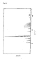
- I ref ( ⁇ ) is shown in FIG. 16 and in this case, a range of from 380 nm to 420 nm is sufficient as the interval.
- the former Nabs is in proportion to the amount determined in accordance with the (Formula 2). 1 R ⁇ ⁇ ⁇ I ref ⁇ ⁇ d ⁇ - ⁇ ⁇ ⁇ I ⁇ ⁇ d ⁇
- I( ⁇ ) is a reflection spectrum when a sample is attached to measure its ⁇ q .
- the integral range of (Formula 2) is made equal to that defined for (Formula 1).
- the second term of (Formula 2) corresponds to the number of photons generated by the reflection of excitation light by the sample, that is, the number of photons obtained by subtracting, from the total number of photons generated from the sample, photons generated by the excitation light through photoluminescence.
- the internal quantum efficiency ⁇ i is a quotient obtained by dividing the number of photons N PL generated by photoluminescence by the number of photons Nabs absorbed by the sample.
- the N PL is in proportion to an amount determined by (Formula 3): ⁇ ⁇ ⁇ I ⁇ ⁇ d ⁇
- an integral interval is limited to a wavelength region of photons generated from the sample by photoluminescence, whereby contribution of the photons reflected by the sample is removed from I( ⁇ ). More specifically, concerning the lower limit of the integral of (Formula 3), the upper end of the integral of (Formula 1) is omitted and a region appropriate for including the spectrum derived from photoluminescence is used as the upper end.
- FIG. 17 is an example of I( ⁇ ).
- either a divalent Eu or trivalent Eu can be used as an activator Eu, but they are different in the transition process of light emission.
- the divalent Eu tends to be excited by ultraviolet light having a longer wavelength so that divalent Eu is preferred.
- the term "Eu concentration" means the Eu concentration determined by the number of divalent Eu(s). When a phosphor contains both the divalent Eu(s) and trivalent Eu(s), the Eu concentration is determined by the number of divalent Eu(s).
- the second light emitter is required to contain a phosphor capable of satisfying any one of the above-described conditions (i) to (iv). Incorporation of a phosphor capable of satisfying the conditions 1 and 3 is however particularly preferred, because it enables manufacture of a light emitting device having a higher emission intensity.
- the materials constituting the phosphor are preferred. It is more preferred to select the materials from those having a crystal phase having the chemical composition of the below-described formulas [1] to [4] (which may be called "crystal phases of the formulas [1] to [4], simply).
- the desired phosphor tends to be available by selecting the preferred crystal phase from those of the formulas [1] to [4].
- the phosphor may comprise, as a component other than the crystal phase, a light scattering substance and the like within an extent not impairing its performance.
- the phosphor contains the crystal phase usually in an amount of 10 wt.% or greater, preferably 50 wt.% or greater, more preferably 80 wt.% or greater.
- the light emitting device of the present invention having the second light emitter containing a phosphor having any one of the crystal phases of the formulas [1] to [4] is novel and has emission intensity superior to that of the conventional light emitting device.
- M 1 s each represents a metal element other than Eu and Sr. In view of emission intensity and the like, it is preferred to adjust the total amount of Ba, Mg, Ca, Zn and Mn in M 1 s to 70 mol% or greater. It is more preferred to adjust the total amount of Ba, Mg and Ca in M 1 s to 70 mol% or greater. It is still more preferred to adjust the total amount of Ba, Mg and Ca in M 1 s to 90 mol% or greater. It is still more preferred that M 1 s are all composed of at least one element selected from the group consisting of Ba, Mg, Ca, Zn and Mn and it is most preferred that M 1 s are all composed of at least one element selected from the group consisting of Ba, Mg and Ca.
- a metal element other than the above-described ones is incorporated as M 1
- a metal element having an equal valence number to Sr or these 5 metal elements (Ba, Mg, Ca, Zn and Mn)
- Ba, Mg, Ca, Zn and Mn a metal element having an equal valence number
- a small amount of a monovalent, trivalent, tetravalent, pentavalent or hexavalent metal element may be introduced for the purpose of accelerating crystallization of a complex oxide caused by the diffusion, in solid, of the divalent metal element and emission center Eu 2+ upon sintering.
- a portion of Sr 2+ in an Sr 5 (PO 4 ) 3 Cl:Eu phosphor can be substituted with an equimolar amount of Li + and Ga 3+ while maintaining charge compensation effects. It may also possible to substitute with a metal element which will serve as a sensitizer.
- X represents a monovalent anionic group other than PO 4 .
- anionic group examples include halogen ions and hydroxyl ion (OH - ).
- the halogen ions include C1 - , F - and Br - , of which C1 - is preferred.
- preferably 50 mol% or greater, more preferably 70 mol% or greater, especially preferably 90 mol% or greater of X is composed of halogen ions.
- the remaining anionic groups may contain a hydroxyl ion and the like.
- 50 mol% or greater, especially 70 mol% or greater, still more preferably 90 mol% or greater of X is composed of C1 - .
- other halogen ions and a hydroxyl ion can be used as the remaining group.
- a molar ratio a of Eu is a number greater than 0 and satisfies a+b ⁇ 5.
- the crystal phase of the formula [1] does not contain M 1 .
- a usually satisfies a ⁇ 4.8, preferably a ⁇ 3, more preferably a ⁇ 2.5, especially preferably a ⁇ 2, most preferably a ⁇ 1.5.
- a satisfying a>0.2, moreover a ⁇ 0.3 is especially preferred in order to obtain a light emitting device composed of a second light emitter having a phosphor satisfying the above-described condition 3 and/or 4.
- the molar ratio b of Sr is 0 or greater, preferably greater than 0 and satisfies a+b ⁇ 5. More specifically, b satisfies 0 ⁇ b ⁇ 5, preferably 0 ⁇ b ⁇ 5.
- b is adjusted to fall within the following range: b ⁇ 0.01, preferably b ⁇ 0.1, more preferably b ⁇ 0.2. In view of emission intensity and the like, it is most preferred to adjust b to fall within the following range: b ⁇ 3, especially b ⁇ 4.
- the crystal phase composed principally of (Sr,Ba,Ca) 5 (PO 4 ) 3 Cl:Eu 2+ the molar ratio of Sr is not narrowly limited.
- Preferred examples of the combination of a and b include (1) a ⁇ 0.1 and b ⁇ 0.01, (2) a ⁇ 0.1 and b ⁇ 0.1, (3) a ⁇ 0.1 and b ⁇ 0.2, (4) a ⁇ 0.2 and b>0.01, (5) a ⁇ 0.2 and b ⁇ 0.1, (6) 0.0001 ⁇ a and b ⁇ 3, (7) 0.001 ⁇ a and b ⁇ 3, (8) 0.005 ⁇ a and b ⁇ 3, (9) 0.0001 ⁇ a and b ⁇ 4, (10) 0.001 ⁇ a and b ⁇ 4, and (11) 0.005 ⁇ a and b ⁇ 4.
- a ⁇ 0.1 and b ⁇ 3 it is especially preferred to satisfy both a ⁇ 0.1 and b ⁇ 3 in order to attain higher emission intensity.
- Example of the combination of a and b preferred from this viewpoint include (1) a ⁇ 0.1 and b ⁇ 3, (2) a ⁇ 0.1 and b ⁇ 4, (3) a ⁇ 0.2 and b ⁇ 3, (4) a ⁇ 0.2 and b ⁇ 4.
- the emission intensity can be increased by satisfying both a>0.2 and b ⁇ 3.
- Examples of the combination of a and b preferred in this viewpoint include (1) a>0.2 and b ⁇ 3, (2) a>0.2 and b ⁇ 4, (3) a ⁇ 0.3 and b ⁇ 3, (4) a ⁇ 0.3 and b ⁇ 4, (5) a ⁇ 0.4 and b ⁇ 3, (6) a ⁇ 0.4 and b ⁇ 4, (7) a ⁇ 0.45 and b ⁇ 3, and (8) a ⁇ 0.45 and b ⁇ 4.
- the c is a number satisfying c ⁇ 2.7, preferably c ⁇ 2.8, more preferably c ⁇ 2.9 and c ⁇ 3.3, preferably c ⁇ 3.2, more preferably c ⁇ 3.1.
- c is preferably 2.7 ⁇ c ⁇ 3.3, more preferably 2.8 ⁇ c ⁇ 3.2, more preferably 2.9 ⁇ c ⁇ 3.1.
- d stands for a number satisfying d ⁇ 0.9, preferably d ⁇ 0.93, more preferably d ⁇ 0.95 and d ⁇ 1.1, preferably d ⁇ 1.07, more preferably d ⁇ 1.05.
- d is 0.9 ⁇ d ⁇ 1.1, preferably 0.93 ⁇ d ⁇ 1.07, more preferably 0.95 ⁇ d ⁇ 1.05.
- a 5 (PO 4 ) 3 Cl (A representing an alkaline earth metal) has a hexagonal crystal structure and its space group is P6 3 /m.
- the crystal phase of the formula [1] has a crystal structure of A 5 (PO 4 ) 3 Cl as described above.
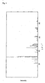
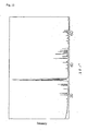
- a typical X-ray diffraction pattern (from powder X-ray diffraction data base) of Sr 5 (PO 4 ) 3 Cl is shown in FIG. 1 .
- the Sr site of Sr 5 (PO 4 ) 3 Cl can be substituted with a divalent metal such as Ba, Mg, Ca, Zn or Mn within a broad composition range. It can also be substituted with a metal having a different valence such as Na or La if its amount is small. Its Cl site can be substituted with an anionic species such as F, Br or OH without changing the structure.
- the crystal phase in the present invention corresponds to that having as a matrix a substituted product using Sr as a cationic species and the cation site substituted with Eu 2+ as an activator.
- the phosphor containing the crystal phase of the formula [1] is excited by light of 350-415 nm from the first light emitter and generates visible light having very high emission intensity.
- the second light emitter containing the phosphor satisfying the above-described conditions (iii) and/or (iv) tends to be available by selecting a preferable phosphor, as that to be incorporated in the second light emitter, from the phosphors of the formula [1].
- M 2 represents at least one element selected from the group consisting of Ba, Sr and Ca.
- the cation M 2' substituted at the site M 2 is a monovalent metal element or a divalent one having a relatively large ion radius. It represents a monovalent metal element or a divalent metal element (except Ba, Sr, Ca and Eu) having a radius of 0.92 ⁇ or greater in the divalent form upon coordination number 6. Specific examples include K, Sm, Pb and Na.
- the coordination number of oxygen is 6 in M 2 and M 3 sites, so that in the present invention, M 2' and M 3' are distinguished therefrom by the cationic radius of the divalent metal element upon coordination number 6.
- a ratio of the total amount of Ba, Sr and Ca in the sum of M 2 and M 2' is preferably adjusted to 80 mol% or greater. It is more preferred that a ratio of Ba in the sum of M 2 and M 2' is 30 mol% or greater and at the same time, a ratio of Sr or Ca in the sum of M 2 and M 2' is 20 mol% or greater.
- M 3 represents at least one element selected from the group consisting of Mg and Zn.
- the cation M 3' substituted at the site M 3 is a relatively small divalent cation. It represents a divalent metal element (except Mg and Zn) having a radius less than 0.92 ⁇ in the divalent form upon coordination number 6. Specific examples include Zn, Mn, V and Zr.
- a ratio of the total amount of Mg and Zn in the sum of M 3 and M 3' is preferably adjusted to 80 mol% or greater.
- M 4 represents at least one element selected from the group consisting of Al, Ga and Sc, preferably Al.
- M 4' represents a trivalent metal element (except Al, Ga and Sc) and specific examples of it include Y, In and Lu.
- a ratio of A1 in the sum of elements M 4 and M 4' is preferably adjusted to 80 mol% or greater.
- a monovalent, trivalent, tetravalent, pentavalent or hexavalent metal element as M 2' and M 3' and a monovalent, divalent, tetravalent, pentavalent or hexavalent metal element as M 4' may be introduced in a small amount within an extent not impairing the advantage of the present invention.
- a portion of Ba 2+ in a BaMgAl 10 O 17 :Eu phosphor can be substituted with an equimolar amount of Li + and Ga 3+ while maintaining charge compensation effects.
- it may be substituted with a metal element such as Mn which will serve as a sensitizer.
- the molar ratio f of Eu in the formula [2] is a number satisfying f ⁇ 0.11, preferably f ⁇ 0.15 and f ⁇ 0.99, preferably f ⁇ 0.85.
- f ⁇ 0.11 preferably f ⁇ 0.15 and f ⁇ 0.99, preferably f ⁇ 0.85.
- the e stands for a number satisfying (e+f) ⁇ 0.9, preferably (e+f) ⁇ 0.95, more preferably (e+f) ⁇ 0.98 and (e+f) ⁇ 1.1, preferably (e+f) ⁇ 1.05, more preferably (e+f) ⁇ 1.02.
- the g stands for a number satisfying g ⁇ 0.9 and g ⁇ 1.1.
- the h stands for a number satisfying h ⁇ 9 and h ⁇ 11.
- the i stands for a number satisfying i ⁇ 15.3 and i ⁇ 18.7.
- the crystal of BaMgAl 10 O 17 has a hexagonal system and its space group is P6 3 /mmc.
- the crystal structure represented by the formula [2] is usually the above-described BaMgAl 10 O 17 structure.
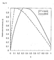
- FIG. 20 a typical X-ray diffraction pattern (from Powder X-ray Diffraction Data Base) of BaMgAl 10 O 17 .
- (Ba,Sr,Ca) (Mg,Zn)Al 10 O 17 Ba 2+ , Sr 2+ , or Ca 2+ is located in an intermediate layer sandwiched between spinnel blocks made of Al 3+ and O 2- , while Mg 2+ or Zn 2+ is located at a substituted position of the Al 3+ .
- the coordination number of oxygen around Ba 2+ site and Mg 2+ site is six.
- a divalent metal element such as Ba, Sr and Ca can form a solid solution with the Ba 2+ site within a broad composition range.
- the Ba 2+ site may be substituted with a divalent metal element other than B, Sr or Ca in such a manner if its amount is small, because it does not adversely affect the emission intensity.
- a trivalent metal such as Ga and B can form a solid solution with the Al 3+ site within a specific composition range.
- the Al 3+ site can be substituted with a trivalent metal such as Ga or B in such a manner if its amount is small, because it does not adversely affect the emission intensity.
- the crystal phase corresponds to a substance having such a substituted product as a matrix and Eu 2+ as an activator and moreover, having a markedly increased Eu 2+ amount.
- the phosphor containing the crystal phase of the formula [2] is excited by light of 350-415 nm from the first light emitter and generates visible light with remarkably high emission intensity.
- the second light emitter containing the phosphor with the crystal phase satisfying the above-described conditions (i) and/or (ii) tends to be available by selecting the crystal phase, as a crystal phase to be incorporated in the second light emitter, from the crystal phases of the formula [2].
- the crystal phase of BaMgAl 10 O 17 is known and it is known that its Ba site can be substituted with the other divalent metal element such as Ca, Sr or Eu 2+ and its Mg site can be substituted with the other divalent metal element such as Zn.
- a substance having BaMg 2 Al 16 O 27 as a chemical composition and substituted with Eu 2+ is also known.
- a phosphor having a crystal phase of Ba 1-x Eu x MgAl 10 O 17 for example, the former one and that having a crystal phase Ba 1-x Eu x Mg 2 Al 16 O 21 , for example, the latter one can be used as a blue light emitting phosphor of a fluorescent lamp and it makes use of light emission, excited by short ultraviolet rays at Hg resonance line at 254 nm.
- the emission intensity of these crystal phases is very high.
- the present inventors have completed the present invention.
- the present invention is based on the finding that compared with blue light emitting BaMgAl 10 O 17 :Eu having Eu at a molar ratio of from 0.05 to 0.1 or yellow light emitting Y 3 Al 5 O 12 :Ce, the above-described phosphor displays a particularly high emission intensity by light excitation at around 400 nm.
- M 5 s represent metal elements comprising at least one element selected from the group consisting of Ba, Sr and Ca in a total amount of 90 mol% or greater, preferably 95 mol% or greater. It is preferred that all of M 5 s are at least one element selected from the group consisting of Ba, Sr and Ca. As a result, higher emission intensity can be attained.
- the crystal phase preferably comprises Ba and/or Sr as M 5 , especially preferably Ba.
- the molar ratio of Ba to Sr is preferably 0.05 or greater, because it facilitates control of emission wavelength and brings higher emission intensity.
- the molar ratio of Sr may be 0 (which means an infinite molar ratio of Ba), but the molar ratio of Ba is preferably adjusted to not greater than 100 without omitting Sr.
- M 6 represents a metal element comprising at least one element selected from the group consisting of Mg and Zn in a total amount of 90 mol% or greater, preferably 95 mol% or greater. It is preferred that all the elements of M 6 s are at least one element selected from the group consisting of Mg and Zn. As a result, higher emission intensity can be attained.
- the crystal phase preferably contains Mg as M 6 .
- M 7 represents a metal element comprising at least one element selected from the group consisting of Si and Ge in a total amount of 90 mol% or greater, preferably 95 mol% or greater, more preferably 97 mol% or greater. It is preferred that all the elements of M 7 s are at least one element selected from the group consisting of Si and Ge. As a result, higher emission intensity can be attained.
- the crystal phase preferably comprises Si as M 7 .
- metal elements other than the above-described ones may be incorporated in the crystal with 10 mol%, preferably 5 mo%, more preferably 3 mol% as an upper limit.
- incorporation of divalent, divalent and tetravalent metal elements that is, elements having a valence number equal to Ba, Mg and Si, respectively is preferred because it facilitates maintenance of the crystal structure.
- a small amount of monovalent, trivalent, pentavalent or hexavalent metal element may be introduced in the crystal with a view to accelerating crystallization of a complex oxide caused by the diffusion, in solid, of divalent and tetravalent metal elements and Eu 2+ serving as an emission center upon sintering.
- the j stands for a number satisfying j ⁇ 2.5, preferably j ⁇ 2.7, more preferably j ⁇ 2.8, still more preferably j ⁇ 2.9 and j ⁇ 3.3, preferably j ⁇ 3.2, more preferably j ⁇ 3.1.
- the molar ratio k of Eu in the formula [3] stands for a number satisfying k ⁇ 0.0001, preferably k ⁇ 0.001, more preferably k ⁇ 0.003 and k ⁇ 1.0, preferably k ⁇ 0.5, more preferably k ⁇ 0.3, still more preferably k ⁇ 0.15, especially preferably k ⁇ 0.1.
- the j and k preferably satisfy 2.7 ⁇ j+k ⁇ 3.3 in order to obtain a crystal phase with less crystal defects and have higher emission intensity.
- the 1 stands for a number satisfying 1 ⁇ 0.9, preferably 1 ⁇ 0.93, more preferably 1 ⁇ 0.95 and 1 ⁇ 1.1, preferably 1 ⁇ 1.07, more preferably 1 ⁇ 1.05.
- the m stands for a number satisfying m ⁇ 1.8, preferably m ⁇ 1.85, more preferably m ⁇ 1.9 and m ⁇ 2.2, preferably m ⁇ 2.15, more preferably m ⁇ 2.1.
- n stands for a number satisfying n ⁇ 7.2, preferably n ⁇ 7.4, more preferably n ⁇ 7.6, most preferably n ⁇ 7.8 and n ⁇ 8.8, preferably n ⁇ 8.6, more preferably n ⁇ 8.4, most preferably n ⁇ 8.2.
- the j+k, 1, m and n are usually 3, 1, 2 and 8, respectively. They however fall within a permissible range embracing these values, because appearance of some cation deficiencies, oxygen deficiencies or interstitial atoms has little influence on the fluorescence performance.
- the typical crystal structure of the phosphor represented by the formula [3] is a Ba 3 MgSi 2 O 8 , Sr 3 MgSi 2 O 8 or Ca 3 MgSi 2 O 8 structure.
- the Ca 3 MgSi 2 O 8 structure is usually called merwinite.
- the Ba 3 MgSi 2 O 8 and Sr 3 MgSi 2 O 8 structures are not strictly merwinite but are presumed to be analogous thereto.
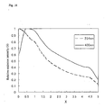
- FIGS. 24, 25 and 26 X-ray diffraction patterns of Ba 3 MgSi 2 O 8 , Sr 3 MgSi 2 O 8 and Ca 3 MgSi 2 O 8 (from Powder X-ray Diffraction Data base) are shown. Judging from that in these crystal structures, a composition range.of divalent metals including Ba, Sr and Ca permitting the formation of a solid solution is wide, they have a similar structure.
- the crystal phase of the phosphor represented by the formula [3] corresponds to that obtained by substituting a substance having a Ba 3 MgSi 2 O 8 , Sr 3 MgSi 2 O 8 or Ca 3 MgSi 2 O 8 structure with Eu 2+ as an activator.
- the crystal phase such as Ba 3 MgSi 2 O 8 or Sr 3 MgSi 2 O 8 is known and it is also known that Ba or Sr can be substituted with other divalent metal element such as Eu 2+ .
- the present invention is based on the finding that when a phosphor containing a crystal phase having the chemical composition of the formula [3] including the chemical composition such as Ba 3-x Eu x MgSi 2 O 8 or Sr 3-x Eu x MgSi 2 O 8 is exposed to light of 350-415 nm from the first light emitter, it emits light having remarkably higher intensity than the other phosphor.
- the above-described phosphor generates light having overwhelmingly high intensity than blue light emitting BaMgAl 10 O 17 :Eu or yellow light emitting Y 3 Al 5 O 12 :Ce.
- the phosphor containing the crystal phase of the formula [3] is excited by light of 350-415 nm from the first light emitter and generates visible light having remarkably high emission intensity.
- M 8 represents a metal element which has at least one valence but is other than Eu, P and B. From the viewpoints of color rendering property, emission intensity and the like, it represents a metal element which contains Ca and at the same time, contains Ca and Mg in a total amount of 80 mol% or greater. A proportion of Ca in the total amount of Ca and Mg contained in M 8 is preferably 40 mol% or greater. It is more preferred that M 8 is at least one element selected from the group consisting of Ca and Mg and contains at least 40 mol% of Ca.
- a metal element other than Ca and Mg is added as M 8 to the crystal
- a metal element having the same valence with Ca and Mg that is, a divalent metal element such as Sr, Zn, Ba, Pb or Sn, preferably Sr, Zn or Ba
- a divalent metal element such as Sr, Zn, Ba, Pb or Sn, preferably Sr, Zn or Ba
- a small amount of a monovalent, trivalent, tetravalent, pentavalent or hexavalent metal element may be introduced as a metal element in M for the purpose of accelerating crystallization of a complex oxide caused by the diffusion, in solid, of the divalent metal element and emission center Eu 2+ upon sintering.
- a portion of Ca 2+ in an Eu 0.15 Ca 2.85 (PO 4 ) 2 phosphor can be substituted with an equimolar amount of Li + and Ga 3+ while maintaining charge compensation effects. It may be also possible to substitute it with a metal element which will serve as a sensitizer in order to control the emission wavelength or emission intensity.
- Z represents an anionic group other than PO 4 3- and BO 3 3- and specific examples include hydroxyl ion (OH - ), metal oxide anions and halogen ions.
- the metal oxide anions include SiO 4 4- , SiO 3 2- , TiO 3 2- and ZrO 3 2-
- the halogen ions include F - , Cl - , Br - and I - . Examples are however not limited thereto.
- the molar ratio o of Eu in the formula [4] is 0.003 or greater, preferably 0.015 or greater in consideration of the color rendering property and emission intensity. Its upper limit is 2.1 or less, preferably 1 or less. When the molar ratio o of Eu 2+ serving as an emission center ion is too small, the emission intensity tends to lower.
- the emission intensity When it is too large, on the other hand, the emission intensity also tends to decrease owing to a phenomenon called concentration quenching.
- the p is a number satisfying 2.7 ⁇ (o+p) ⁇ 3.3.
- the fundamental stoichiometric molar ratio (o+p) when Z is neglected as an impurity is 3.
- Appearance of some cation deficiencies or anion deficiencies has less influence on the intended fluorescence performance of the present invention so that (o+p) can be used within the above-described range.
- the molar ratio q of the PO 4 group stands for a number satisfying 1.2 ⁇ q ⁇ 2. From the viewpoints of color rending property, emission intensity and the like, q is preferably 1.6 or greater. In the above-described formula [4], the total molar ratio of the PO 4 and BO 3 groups serving as main anions is 2. The existence of the BO 3 group does not have a serious adverse effect on the color rendering property, emission intensity and the like.
- the molar ratio r of Z which is an anion other than the PO 4 and BO 3 groups is a number satisfying 0 ⁇ r ⁇ 0.1.
- the anion Z may be incorporated in the crystal if its amount is not large enough to adversely affect the intended fluorescence performance of the present invention. The smaller its content, the better.
- the r is preferably 0.05 or less..
- a substance having an orthophosphate A 3 (PO 4 ) 2 (in which A represents an alkaline earth metal) as a crystal matrix and activated with Eu 2+ is known as an ordinary phosphor excited at 254 nm.
- the present invention is however based on the finding that the emission intensity caused by the excitation of light at around 400 nm and the half-width of its emission peak differ largely, depending on the kind of the alkaline earth metal A of A 3 (PO 4 ) 2 ; a substance of A 3 (PO 4 ) 2 :Eu 2+ containing Ca or Ca-Mg complex cation as A emits blue light with high emission intensity, exposed to excitation light of 350-415 nm; and a distribution of emission wavelength - emission intensity relating to a great improvement in color rendering property is wide, in other words, the half-width is large so that the phosphor can provide a high color rendering property.
- the phosphor to be used in the present invention can be obtained by preparing a pulverized mixture in a dry method, more specifically, by pulverizing, in a dry pulverizer such as hammer mill, roll mill, ball mill or jet mill, compounds as M 1 source, X source, PO 4 source and Sr source and compounds as an element source for an emission center ion (Eu) when the phosphor contains the crystal phase of the formula [1], compounds as a M 2 source, M 2' source, M 3 source, M 3' source, M 4 source and M 4' source and compounds as an element source for an emission center ion (Eu 2+ ) when the phosphor contains the crystal phase of the formula [2], compounds as a M 5 source, M 6 source and M 7 source and compounds as an element source for an emission center ion (Eu 2+ ) when the phosphor contains the crystal phase of the formula [3], or compounds as M 8 source, PO 4 source, BO 3 source and Z source and compounds as an element source for an emission center
- pulverizing and mixing methods that using a liquid medium is preferred because a compound to be added in a small amount such as a compound as an element source for emission center ion must be mixed and dispersed uniformly.
- the latter wet method is preferred also for the compounds as the other element sources, because it enables preparation of a uniform mixture of them.
- Heating is performed in a heat-resistant container such as alumina or quartz crucible or tray ordinarily at 700 to 1700°C, preferably at 900 to 1500°C in an atmosphere of a single gas such as air, oxygen, carbon monoxide, carbon dioxide, nitrogen, hydrogen or argon, or a mixture thereof for 10 minutes to 24 hours.
- a heat-resistant container such as alumina or quartz crucible or tray ordinarily at 700 to 1700°C, preferably at 900 to 1500°C in an atmosphere of a single gas such as air, oxygen, carbon monoxide, carbon dioxide, nitrogen, hydrogen or argon, or a mixture thereof for 10 minutes to 24 hours.
- the heating is followed by washing, drying and classification as needed.
- atmosphere necessary for obtaining an ion state (number of valence) of the element of an emission center ion enough for contributing light emission is selected.
- a neutral or reducing atmosphere such as carbon monoxide, nitrogen, hydrogen or argon is preferred, but an oxidizing atmosphere such as air or oxygen can also be adopted under properly selected conditions.
- Examples of the compounds as M 1 to M 8 sources, M 2' to m 4' sources, Sr source and Eu source include oxides, hydroxides, carbonates, nitrates, sulfates, oxalates, carboxylates, halides, hydrogen phosphates and phosphates of M 1 to M 8 , M 2' to M 4' , Sr and Eu.
- Specific examples of the compounds as a Sr source include SrO, Sr(OH) 2 ⁇ 8H 2 O, SrCO 3 , Sr(NO 3 ) 2 , Sr(OCO) 2 ⁇ H 2 O, Sr(OCOCH 3 ) 2 ⁇ 0.5H 2 O and SrCl 2 .
- the compounds as a Ba source include BaO, Ba(OH) 2 ⁇ 8H 2 O, BaCO 3 , Ba(NO 3 ) 2 , BaSO 4 , Ba(OCO) 2 ⁇ 2H 2 O, Ba(OCOCH 3 ) 2 and BaCl 2 .
- the compounds as a Mg source include MgO, Mg(OH) 2 , MgCO 3 , Mg(OH) 2 , 3MgCO 3 ⁇ 3H 2 O, Mg(NO 3 ) 2 ⁇ 6H 2 O, Mg(OCO) 2 ⁇ 2H 2 O, Mg(OCOCH 3 ) 2 ⁇ 4H 2 O, and MgCl 2 .
- Specific examples of the compounds as a Ca source include CaO, Ca(OH) 2 , CaCO 3 , Ca(NO 3 ) 2 ⁇ 4H 2 O, Ca(OCO) 2 ⁇ H 2 O, Ca(OCOCH 3 ) 2 ⁇ H 2 O, and CaCl 2 .
- the compounds as a Zn source include ZnO, Zn(OH) 2 , ZnCO 3 , Zn(NO 3 ) 2 ⁇ 6H 2 O, Zn(OCO) 2 , Zn(OCOCH 3 ) 2 and ZnCl 2 .
- the compounds as a Mn source include MnO 2 , Mn 2 O 3 , Mn 3 O 4 , MnOOH, MnCO 3 , Mn(NO 3 ) 2 , Mn(OCOCH 3 ) 2 ⁇ 2H 2 O, Mn(OCOCH 3 ) 3 ⁇ nH 2 O, and MnCl 2 ⁇ 4H 2 O.
- Specific examples of the compounds as an element source for Eu 2+ include Eu 2 O 3 , Eu(OCOCH 3 ) 3 ⁇ 4H 2 O, EuCl 3 ⁇ 6H 2 O and Eu 2 (OCO) 3 ⁇ 6H 2 O.
- Examples of the compounds as a PO 4 source include hydrogen phosphates, phosphates, metaphosphates, pyrophosphates of M 1 , M 8 , Eu and NH 4 , P 2 O 5 , PX 3 , PX 5 , M 2 PO 4 X, phosphoric acid, metaphosphoric acid and pyrophosphoric acid.
- Examples of the compounds as a BO 3 source include borates, hydrogen borates, tetraborates, octaborates, diborates, and pentaborates of M 8 , Eu and NH 4 , boric acid and boron oxide. Of these, borates and hydrogen borates of M 8 , Eu and NH 4 , boric acid and boron oxide are preferred.
- Examples of the compounds as an X source include M 1 X, NH 4 X, HX and M 1 2 PO 4 X.
- Examples of the compounds as a Z source include M 8 2 SiO 4 , M 8 SiO 3 , M 8 TiO 3 , M 8 ZnO 3 , M 8 F 2 , M 8 Cl 2 , M 8 Br 2 , NH 4 F, NH 4 Cl, NH 4 Br, HF, HCl and HBr.
- a proper one is selected in consideration of the chemical composition, reactivity and sintering without emitting a gas such as NO x and SO x .
- the first light emitter which irradiates light to the phosphor emits light having a wavelength of 350-415 nm.
- a light emitter generating light with a peak wavelength within a wavelength range of from 350 to 415 nm is preferred. More preferred from the viewpoint of emission efficiency is a light emitter emitting light having a peak wavelength within a wavelength range of from 390 to 410 nm.
- Specific examples of the first light emitter include light emitting diode (LED) and laser diode (LD). The laser diode is more preferred, because it consumes less power.
- a GaN-based LED and LD using a GaN compound semiconductor are especially preferred, because their emission output or external quantum efficiency is by far great compared with an SiC-based LED emitting light of this region so that very bright light emission is available at a considerably low electricity by using it in combination with the above-described phosphor.
- a GaN-based diode has emission intensity at least 100 times that of an SiC-based diode.
- the GaN-based LED or LD preferably has an Al X Ga Y N luminescent layer, GaN luminescent layer or In X Ga Y N luminescent layer.
- the GaN-based LED having an In x Ga Y N luminescent layer is especially preferred because it has remarkably high emission intensity
- the GaN-based LD having a multiple quantum well structure with an In X Ga Y N layer and a GaN layer is especially preferred because of remarkably high emission intensity
- X+Y is usually a value within a range of from 0.8 to 1.2.
- the GaN-based LED that with a luminescent layer having Zn or Si doped therein or no dopant therein is preferred, because it facilitates control of luminescent properties.
- the GaN-based LED has such a luminescent layer, p layer, n layer, electrode and substrate as principal constituents, of which that having a hetero structure in which the luminescent layer has been sandwiched between the n type and p type Al X Ga Y N layers, GaN layers or In X Ga Y N layers is preferred because of having high emission efficiency; that having, as the hetero structure, a quantum well structure is more preferred because of having higher emission efficiency.
- a vertical cavity surface emitting light emitter especially a vertical cavity surface light emitting type GaN laser diode as the first light emitter is especially preferred in order to heighten the emission efficiency of the whole light emitting apparatus.
- the vertical cavity surface emitter generates intense light in the plane direction of a film.
- light emission in the plane direction can be made more intense than the edge direction of the luminescent layer by controlling the crystal growth of the luminescent layer and at the same time using a reflecting layer successfully.
- a light emitting cross-sectional area per unit emission amount can be made greater than that of a diode emitting light from the edge of the luminescent layer.
- the exposed area can be increased remarkably at the same light intensity, meaning an improvement in irradiation efficiency. As a result, more intense light is available from the phosphor.
- the second light emitter is preferably in the film form.
- the vertical cavity surface emitting type light emitter has a large light-emitting cross-sectional area so that formation of the second light emitter in the film form in the cross-sectional direction makes it possible to heighten the emission intensity from the phosphor, because the irradiation cross-sectional area from the first light emitter to the phosphor becomes large per unit amount of the phosphor.
- the second light emitter in the film form When a vertical cavity surface emitting type is used as the first light emitter and the second light emitter in the film form is used, it is preferred to bring the second light emitter in the film form into direct contact with the light emitting surface of the first light emitter.
- the term "bring into direct contact” as used herein means “bring the first light emitter into close contact with the second light emitter without having air or another gas inserted therebetween".
- FIG. 2 is a schematic perspective view illustrating the positional relationship between the first light emitter and the second light emitter in one example of the light emitting device of the present invention, in which indicated at numeral 1 is a second light emitter in the film form having the phosphor, 2 a vertical cavity surface emitting GaN-based LD as the first light emitter, and 3 a substrate.
- These three components can be brought into contact with each other by bringing the LD 2 and the second light emitter 1, which have been prepared separately in advance, into contact at their surfaces by various means including an adhesive; or forming (as a film) or molding the second light emitter over the luminescent surface of the LD 2.
- the LD 2 can be brought into contact with the second light emitter 1.
- Light from the first light emitter or second light emitter usually scatters in all directions.
- powder of the phosphor to be used as the second light emitter is dispersed in a resin, a portion of light is reflected when it comes outside of the resin so that the light can be adjusted to one direction to some extent. Light can thus be induced to an efficient direction to some extent so that use of a dispersion of the phosphor powder in a resin as the second light emitter is preferred.
- the phosphor powder that having an average particle size of from 0.5 to 15 ⁇ m is usually employed.
- the average diameter is preferably 0.8 to 5 ⁇ m, more preferably from 0.8 to 2 ⁇ m.
- a dispersion of the phosphor in a resin has another advantage that it can heighten the intensity of light from the second light emitter, because the total area of light irradiated from the first light emitter toward the second light emitter becomes large.
- the resin which can be used for this purpose include epoxy resin, polyvinyl resin, polyethylene resin, polypropylene resin and polyester resin.
- the epoxy resin is preferred because the phosphor powder can be well dispersed therein.
- a weight ratio of the phosphor powder to the whole resin is usually from 10 to 95%, preferably from 20 to 90%, more preferably from 30 to 80%.
- the amount of the phosphor is too large, agglomeration of powder happens to lower the emission efficiency, while too small amount happens to deteriorate the emission efficiency owing to absorption or scattering of light in the resin.
- the light emitting device of the present invention is capable of emitting white light by mixing light from the first light emitter and light from the second light emitter. Upon emission, a color filter may be used as needed. By making the light emitted from the device white, an object to be exposed to the light of this light emitting device has a high color rendering property. This is an important point upon application of this light emitting device for illumination use.
- the light emitting device of the present invention is composed of the above-described phosphor as a wavelength conversion material and a light emitter generating light of 350-415 nm.
- the phosphor absorbs light of 350-415 nm generated by the light emitter, whereby visible light with good color rendering property and high intensity can be emitted under any using environment. It is suited as a backlight source, light source for traffic signals, and a light source for image display device such as color liquid-crystal display or vertical cavity surface emitting illuminator.
- FIG. 3 is a schematic cross-sectional view illustrating one example of a light emitting device having a first light emitter (emits light of 350-415 nm) and a second light emitter, in which indicated at numeral 4 is a light emitting device, 5 a mount lead, 6 an inner lead, 7 a first light emitter (which emits light of 350-415 nm), 8 a phosphor-containing resin portion as a second light emitter, 9 a conductive wire and 10 a molding member.
- the light emitting device which is one example of the present invention has a bullet-like shape as illustrated in FIG. 3 .
- the first light emitter (emitter of light with 350-415 nm) 7 is fixed by the phosphor-containing resin portion 8, which has been formed as the second light emitter by mixing and dispersing the phosphor in a binder such as epoxy resin or acrylic resin and then casting the dispersion in the cup.
- the first light emitter 7 and mount lead 5, and the first light emitter 7 and inner lead 6 are electrically connected each other via the conductive wire 9. They are all covered and protected with the molding member 10 made of an epoxy resin or the like.
- a number of light emitting devices 91 are placed on the bottom surface of a square holding case 910 having an opaque inner surface, for example, a white flat inner surface while disposing, outside the case, a power supply and circuit (not illustrated) for driving the light emitting devices 91.
- a diffusion plate 99 such as an opalescent acryl plate is fixed to accomplish uniform light emission.
- the vertical cavity surface emitting illuminator 98 is switched on and a voltage is applied to the first light emitter of the light emitting devices 91, whereby light of 350-415 nm is emitted.
- the phosphor in the phosphor-containing resin portion as the second light emitter absorbs a portion of the light and emits visible light.
- the visible light is mixed with blue light and the like not absorbed by the phosphor.
- the resulting light with high color rendering property transmits through the diffusion plate 99 and outputs in the upward direction of the diagram, whereby light with uniform brightness is available in the plane of the diffusion plate 99 of the holding case 910.
- the relative emission intensity (i) is a value provided that the emission intensity of the phosphor obtained in Comparative Example 1 is 100.
- the relative emission intensity (i) is a value provided that the emission intensity of the phosphor obtained in Comparative Example 3 excited at each of 400 nm and 254 nm is 100.
- the relative emission intensity (i) is a value provided that the emission intensity of the phosphor obtained in Comparative Example 4 is 100.
- the relative integrated intensity is a value provided that the integrated intensity of the phosphor obtained in Comparative Example 6 is 1.
- the relative emission intensity (i) is a value provided that the emission intensity of the phosphor obtained in Example 40 excited at each of 400 nm and 254 nm is 100.
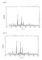
- FIG. 4 The X-ray diffraction pattern of the resulting phosphor is shown in FIG. 4 . From the diagram, it has been found that the peak pattern of FIG. 4 is crystallographically identical to that of Sr 5 (PO 4 ) 3 Cl of FIG. 1 .
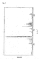
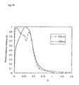
- the emission spectrum of the resulting phosphor excited at 400 nm which is a dominant wavelength of the ultraviolet region of a GaN light emitting diode is shown in FIG. 5 .
- the wavelength of emission peak and relative emission intensity (i) when the resulting phosphor was excited at 400 nm that is, a dominant wavelength of the ultraviolet region of a GaN light emitting diode; and a quantum absorption efficiency ⁇ q of the phosphor and a product ⁇ q ⁇ i of the quantum absorption efficiency ⁇ q and the internal quantum efficiency ⁇ i of the phosphor as measured using a reflector having a reflectance of 98% are shown.
- FIG. 6 The X-ray diffraction pattern of the resulting phosphor is shown in FIG. 6 . From the diagram, it has been found that the peak pattern of FIG. 6 is crystallographically identical to that of Sr 5 (PO 4 ) 3 Cl of FIG. 1 .
- the resulting phosphor was excited at 400 nm, that is, a dominant wavelength of the ultraviolet region of a GaN light emitting diode.
- the wavelength of its emission peak, relative emission intensity (i), a quantum absorption efficiency ⁇ q of the phosphor and a product ⁇ q ⁇ i of the quantum absorption efficiency ⁇ q and the internal quantum efficiency ⁇ i of the phosphor as measured using a reflector having a reflectance of 98% are shown.
- the Eu-Eu mean distance was 6.7 ⁇ .
- Example 2 In a similar manner to Example 1 except for the use of 0.1055 mole of SrHPO 4 , 0.0176 mole of SrCl 2 and 0.0264 mole of Eu 2 O 3 as raw materials instead, a phosphor Sr 3.5 Eu 1.5 (PO 4 ) 3 Cl was prepared.
- FIG. 7 The X-ray diffraction pattern of the resulting phosphor is shown in FIG. 7 . From the diagram, it has been found that the peak pattern of FIG. 7 is crystallographically identical to that of Sr 5 (PO 4 ) 3 Cl of FIG. 1 .
- the resulting phosphor was excited at 400 nm, that is, a dominant wavelength of the ultraviolet region of a GaN light emitting diode and emission spectrum was measured.
- the wavelength of its emission peak, relative emission intensity (i), and a quantum absorption efficiency ⁇ q of the phosphor and a product ⁇ q ⁇ i of the quantum absorption efficiency ⁇ q and the internal quantum efficiency ⁇ i of the phosphor as measured using a reflector having a reflectance of 98% are shown.
- the Eu-Eu mean distance was 5.9 ⁇ .
- Example 2 In a similar manner to Example 1 except for the use of 0.0879 mole of SrHPO 4 , 0.0176 mole of SrCl 2 , 0.0352 mole of Eu 2 O 3 and 0.0176 mole of (NH 4 ) 2 HPO 4 as raw materials instead, a phosphor Sr 3 Eu 2 (PO 4 ) 3 Cl was prepared.
- FIG. 8 The X-ray diffraction pattern of the resulting phosphor is shown in FIG. 8 . From the diagram, it has been found that the peak pattern of FIG. 8 is crystallographically identical to that of Sr 5 (PO 4 ) 3 Cl of FIG. 1 .
- the resulting phosphor was excited at 400 nm, that is, a dominant wavelength of the ultraviolet region of a GaN light emitting diode and its emission spectrum was measured.
- the wavelength of its emission peak and relative emission intensity (i) are shown in Table 1.
- the Eu-Eu mean distance was 5.3 ⁇ .
- Example 2 In a similar manner to Example 1 except for the use of 0.1055 mole of SrHPO 4 , 0.0484 mole of SrCO 3 , 0.0176 mole of SrCl 2 and 0.00176 mole of CaCo 3 , basic magnesium carbonate (0.00088 mole as Mg) and 0.00088 mole of Eu 2 O 3 as raw materials instead, a phosphor Sr 4.875 Ca 0.05 Mg 0.025 Eu 0.05 (PO 4 ) 3 Cl was prepared.
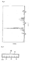
- the X-ray diffraction pattern of the resulting phosphor is shown in FIG. 10 . From the diagram, it has been found that the peak pattern of FIG. 10 is crystallographically identical to that of Sr 5 (PO 4 ) 3 Cl of FIG. 1 .
- the resulting phosphor was excited at 400 nm, that is, a dominant wavelength of the ultraviolet region of a GaN light emitting diode and its emission spectrum was measured.
- the Eu-Eu mean distance was 18.2 ⁇ .
- Example 2 In a similar manner to Example 1 except for the use of 0.1055 mole of SrHPO 4 0.0396 mole of SrCO 3 , 0.00879 mole of BaCO 3 , basic magnesium carbonate (0.00264 mole as Mg), 0.0176 mole of BaCl 2 , and 0.00088 mole of Eu 2 O 3 as raw materials instead, a phosphor Sr 4.125 Ba 0.75 Mg 0.075 Eu 0.05 (PO 4 ) 3 Cl was prepared.
- the X-ray diffraction pattern of the resulting phosphor is shown in FIG. 11 . From the diagram, it has been found that the peak pattern of FIG. 11 is crystallographically identical to that of Sr 5 (PO 4 ) 3 Cl of FIG. 1 .
- the resulting phosphor was excited at 400 nm, that is, a dominant wavelength of the ultraviolet region of a GaN light emitting diode and its emission spectrum was measured. The wavelength of its emission peak and relative emission intensity (i) are shown in Table 1.
- the Eu-Eu mean distance was 18.2 ⁇ .
- Example 2 In a similar manner to Example 1 except for the use of 0.0527 mole of SrHPO 4 , 0.0176 mole of SrCl 2 , 0.0527 mole of Eu 2 O 3 and 0.0527 mole of (NH 4 ) 2 HPO 4 as raw materials instead, a phosphor Sr 2 Eu 3 (PO 4 ) 3 Cl was prepared.
- FIG. 12 The X-ray diffraction pattern of the resulting phosphor is shown in FIG. 12 . From the diagram, it has been found that the peak pattern of FIG. 12 is crystallographically identical to that of Sr 5 (PO 4 ) 3 Cl of FIG. 1 .
- the resulting phosphor was excited at 400 nm, that is, a dominant wavelength of the ultraviolet region of a GaN light emitting diode and its emission spectrum was measured.
- Table 1 the wavelength of its emission peak and relative emission intensity (i), and a quantum absorption efficiency ⁇ q of the phosphor and a product ⁇ q ⁇ i of the quantum absorption efficiency ⁇ q and the internal quantum efficiency ⁇ i of the phosphor as measured using a reflector having a reflectance of 98% are shown.
- the Eu-Eu mean distance was 4.7 ⁇ .
- Example 2 In a similar manner to Example 1 except for the use of 0.0176 mole of SrCl 2 , 0.0791 mole of Eu 2 O 3 and 0.1055 mole of (NH 4 ) 2 HPO 4 as raw materials instead, a phosphor Sr 0.5 Eu 4.5 (PO 4 ) 3 Cl was prepared.
- FIG. 13 The X-ray diffraction pattern of the resulting phosphor is shown in FIG. 13 . From the diagram, it has been found that the peak pattern of FIG. 13 is crystallographically identical to that of Sr 5 (PO 4 ) 3 Cl of FIG. 1 .
- the resulting phosphor was excited at 400 nm, that is, a dominant wavelength of the ultraviolet region of a GaN light emitting diode and its emission spectrum was measured.
- Table 1 the wavelength of its emission peak and relative emission intensity (i), and a quantum absorption efficiency ⁇ q of the phosphor and a product ⁇ q ⁇ i of the quantum absorption efficiency ⁇ q and the internal quantum efficiency ⁇ i of the phosphor as measured using a reflector having a reflectance of 98% are shown.
- the Eu-Eu mean distance was 4.1 ⁇ .
- Example 2 In a similar manner to Example 1 except for the use of 0.1055 mole of SrHPO 4 , 0.0302 mole of SrCO 3 , 0.0199 mole of CaCO 3 , basic magnesium carbonate (0.00088 mole as Mg), 0.0176 mole of BaCl 2 , and 0.00088 mole of Eu 2 O 3 as raw materials instead, a phosphor Sr 3.86 Ba 0.5 Ca 0.565 Mg 0.025 Eu 0.05 (PO 4 ) 3 Cl was prepared.
- FIG. 14 The X-ray diffraction pattern of the resulting phosphor is shown in FIG. 14 . From the diagram, it has been found that the peak pattern of FIG. 14 is crystallographically identical to that of Sr 5 (PO 4 ) 3 Cl of FIG. 1 .
- the resulting phosphor was excited at 400 nm, that is, a dominant wavelength of the ultraviolet region of a GaN light emitting diode and its emission spectrum was measured.
- the wavelength of its emission peak and relative emission intensity (i) are shown in Table 1.
- the Eu-Eu mean distance was 18.2 ⁇ .
- Example 2 In a similar manner to Example 1 except for the use of 0.1055 mole of SrHPO 4 , 0.0121 mole of SrCO 3 , 0.0204 mole of BaCO 3 , 0.0176 mole of CaCO 3 , basic magnesium carbonate (0.00088 mole as Mg), 0.0176 mole of BaCl 2 , and 0.00088 mole of Eu 2 O 3 as raw materials instead, a phosphor Sr 3.345 Ba 1.08 Ca 0.5 Mg 0.025 Eu 0.05 (PO 4 ) 3 Cl was prepared.
- FIG. 15 The X-ray diffraction pattern of the resulting phosphor is shown in FIG. 15 . From the diagram, it has been found that the peak pattern of FIG. 15 is crystallographically identical to that of Sr 5 (PO 4 ) 3 Cl of FIG. 1 .
- the resulting phosphor was excited at 400 nm, that is, a dominant wavelength of the ultraviolet region of a GaN light emitting diode and its emission spectrum was measured.
- the wavelength of its emission peak and relative emission intensity (i) are shown in Table 1.
- the Eu-Eu mean distance was 18.2 ⁇ .
- the emission spectrum of the resulting phosphor excited at 400 nm, that is, a dominant wavelength of the ultraviolet region of a GaN light emitting diode is shown in FIG. 5 .
- the performance of the blue light emitting phosphor obtained in Comparative Example 1 and that obtained in Example 1 was compared.
- Table 1 the wavelength of the emission peak and relative emission intensity (i) when the phosphor was excited at 400 nm, that is, a dominant wavelength in the ultraviolet region of a GaN light emitting diode are shown. From the table, it has been found that the emission intensity of the phosphor of Example 1 is 5.1 times that of the phosphor obtained in Comparative Example 1, when excited at 400 nm.
- Example 2 In a similar manner to Example 1 except for the use of 0.0897 mole of SrHPO 4 , 0.0325 mole of BaCO 3 , 0.0176 mole of CaCO 3 , basic magnesium carbonate (0.00088 mole as Mg), 0.0176 mole of BaCl 2 , 0.0158 mole of BaHPO 4 , and 0.00088 mole of Eu 2 O 3 as raw materials instead, a phosphor Sr 2.55 Ba 1.875 Ca 0.5 Mg 0.025 Eu 0.05 (PO 4 ) 3 Cl was prepared.
- the emission spectrum of the resulting phosphor excited at 400 nm, that is, a dominant wavelength of the ultraviolet region of a GaN light emitting diode is shown in FIG. 5 .
- the performance of the blue light emitting phosphor obtained in Comparative Example 2 and that obtained in Example 1 was compared.
- Table 1 the wavelength of the emission peak and relative emission intensity (i) when the phosphor was excited at 400 nm, that is, a dominant wavelength in the ultraviolet region of a GaN light emitting diode are shown. It has been found from the table that the emission intensity of the phosphor of Example 1 is 5.1 times that of the phosphor obtained in Comparative Example 2, when excited at 400 nm.
- Table 1 Chemical composition of phosphor Wavelength (nm) of emission peak when excited at 400 nm Relative emission intensity (i) when excited at 400 nm ⁇ q ⁇ q ⁇ l Ex. 1 Sr 4.5 Eu 0.5 (PO 4 ) 3 Cl 446 507 0.919 0.677 Ex.
- Example 2 In a similar manner to Example 1 except that the amounts of SrHPO 4 , SrCl 2 , Eu 2 O 3 and (NH 4 ) 2 HPO 4 were changed, a phosphor Sr (5-x) Eu x (PO 4 ) 3 Cl with x falling within a range of from 0.05 to 5 was prepared. The phosphor thus obtained was exposed to light of 254 nm and 400 nm and each emission spectrum was measured.
- FIG. 18 the relationship between x and the emission intensity when excited at each of 254 nm and 400 nm is shown.
- the relative emission intensity (ii) used here means emission intensity at the concentration of x provided that the maximum emission intensity at each of 254 nm and 400 nm is 1.
- each Eu concentration is at least 1.1 times that ( ⁇ 0.05) at the maximum emission intensity upon excitation at 254 nm and it falls within a range of from 0.5 to 9 times that (0.5) at the maximum emission intensity upon excitation at 400 nm.
- Calcium chloride dihydrate (0.01382 mole) and 0.00028 mole of europium chloride hexahydrate were weighed and dissolved in 20 ml of water.
- To the resulting aqueous solution was added 85% phosphoric acid in an amount of 0.00846 mole in terms of phosphoric acid.
- the resulting mixture was transferred into a magnetic dish to give a total amount of from 30 to 40 ml.
- the solution was heated and dried under stirring. The solid remained after drying was collected and pulverized in an agate mortar.
- a portion of the pulverized product was transferred to an alumina crucible and sintered at 1000°C for 2 hours under a nitrogen gas stream containing 4% of hydrogen, whereby a phosphor Ca 4.9 Eu 0.1 (PO 4 ) 3 Cl was prepared.
- the Eu-Eu mean distance in Ca 4.9 Eu 0.1 (PO 4 ) 3 Cl was 13.9 ⁇ .
- the Eu-Eu mean distance was 11.1 ⁇ .
- the Eu-Eu mean distance was 8.8 ⁇ .
- the Eu-Eu mean distance was 8.2 ⁇ .
- the Eu-Eu mean distance was 7.1 ⁇ .
- Calcium chloride dihydrate (0.00948 mole) and 0.00237 mole of europium nitrate hexahydrate were weighed and dissolved in 20 ml of water. To the resulting aqueous solution was added 85% phosphoric acid as phosphoric acid.
- a phosphor Ca( 5-x) EU x (PO 4 ) 3 Cl with x falling within a range of from 0.01 to 1.25 was prepared. The resulting phosphor was exposed to light of each of 254 nm and 400 nm to measure its emission spectrum.
- the relative emission intensity (ii) used here means emission intensity at the concentration x provided that the maximum emission intensity at each of 254 nm and 400 nm is 1.
- the Eu concentrations (mole numbers) at the maximum emission intensity when the phosphor was excited at 400 nm and 254 nm were 0.75 and 0.05, respectively, and the former is greater than the latter. It has also been found that the Eu concentrations in Examples 14 to 17 are each at least 1.1 times the Eu concentration ( ⁇ 0.05) at the maximum emission intensity upon excitation at 254 nm and it falls within a range of from 0.5 to 9 times the Eu concentration (0.5) at the maximum emission intensity upon excitation at 400 nm.
- the resulting phosphor was excited at 400 nm, that is, a dominant wavelength in the ultraviolet region of a GaN light emitting diode and 254 nm, that is, a dominant wavelength of a low-pressure mercury lamp to be used for ordinary fluorescent lamps, whereby the emission spectra were measured.
- Table 3 the wavelength of the emission peak when the phosphor Was excited at 400 nm and the relative emission intensity (i) when the phosphor was excited at each of 400 nm and 254 nm are shown.
- Example 19 In a similar manner to Example 19 except for the use of 0.00570 mole of BaCO 3 , basic magnesium carbonate (0.0114 mole as Mg), 0.0570 mole of ⁇ -Al 2 O 3 , and 0.00285 mole of Eu 2 O 3 as raw materials instead, a phosphor Ba 0.5 Eu 0.5 MgAl 10 O 17 was prepared.
- FIG. 21 The X-ray diffraction pattern of the resulting phosphor is shown in FIG. 21 . From this diagram, it has been found that the peak pattern of FIG. 21 is crystallographically identical to that of BaMgAl 10 O 17 of FIG. 20 .
- the resulting phosphor was excited at 400 nm, that is, a dominant wavelength in the ultraviolet region of a GaN light emitting diode and at 254 nm, that is, a dominant wavelength of a low-pressure mercury lamp to be used for ordinary fluorescent lamps, whereby the emission spectra were measured.
- Table 3 the wavelength of the emission peak when the phosphor was excited at 400 nm and the relative emission intensity (i) when the phosphor was excited at each of 400 nm and 254 nm are shown.
- the Eu-Eu mean distance was 8.5 ⁇ .
- Example 19 In a similar manner to Example 19 except for the use of 0.00912 mole of BaCO 3 , basic magnesium carbonate (0.0114 mole as Mg), 0.0570 mole of ⁇ -Al 2 O 3 , and 0.00114 mole of Eu 2 O 3 as raw materials instead, a phosphor Ba 0.8 Eu 0.2 MgAl 10 O 17 was prepared.
- the resulting phosphor was excited at 400 nm, that is, a dominant wavelength in the ultraviolet region of a GaN light emitting diode and at 254 nm, that is, a dominant wavelength of a low-pressure mercury lamp to be used for ordinary fluorescent lamps, whereby the emission spectra were measured.
- Table 3 the wavelength of the emission peak when the phosphor was excited at 400 nm and the relative emission intensity (i) when the phosphor was excited at each of 400 nm and 254 nm are shown.
- the Eu-Eu mean distance was 11.6 ⁇ .
- Example 19 In a similar manner to Example 19 except for the use of 0.00502 mole of BaCO 3 , 0.00410 mole of CaCO 3 , basic magnesium carbonate (0.0114 mole as Mg), 0.0570 mole of ⁇ -Al 2 O 3 , and 0.00114 mole of Eu 2 O 3 as raw materials instead, a phosphor Ba 0.44 Ca 0.36 Eu 0.2 MgAl 10 O 17 was prepared.
- the resulting phosphor was excited at 400 nm, that is, a dominant wavelength in the ultraviolet region of a GaN light emitting diode to measure its emission spectrum.
- Table 3 the wavelength of the emission peak and the relative emission intensity (i) when the phosphor was excited at 400 nm are shown.
- the Eu-Eu mean distance was 11.6 ⁇ .
- Example 19 In a similar manner to Example 19 except for the use of 0.00502 mole of BaCO 3 0.00410 mole of SrCO 3 , basic magnesium carbonate (0.0114 mole as Mg), 0.0570 mole of ⁇ -Al 2 O 3 , 0.00114 mole of Eu 2 O 3 as raw materials instead, a phosphor Ba 0.44 Sr 0.36 Eu 0.2 MgAl 10 O 17 was prepared.
- the resulting phosphor was excited at 400 nm, that is,' a dominant wavelength in the ultraviolet region of a GaN light emitting diode to measure its emission spectrum.
- Table 3 the wavelength of the emission peak and the relative emission intensity (i) when the phosphor was excited at 400 nm are shown.
- the Eu-Eu mean distance was 11.6 ⁇ .
- Example 19 In a similar manner to Example 19 except for the use of 0.0103 mole of BaCO 3 , basic magnesium carbonate (0.0114 mole as Mg), 0.0570 mole of ⁇ -Al 2 O 3 , and 0.00057 mole of Eu 2 O 3 as raw materials instead, a phosphor Ba 0.9 Eu 0.1 MgAl 10 O 17 having a composition similar to that of the commercially available blue light emitting phosphor was prepared.
- the resulting phosphor was excited at 400 nm, that is, a dominant wavelength in the ultraviolet region of a GaN light emitting diode and at 254 nm, that is, a dominant wavelength of a low-pressure mercury lamp to be used for ordinary fluorescent lamps, whereby the emission spectra were measured.
- Table 3 the wavelength of the emission peak when the phosphor was excited at 400 nm and the relative emission intensity (i) when the phosphor was excited at each of 400 nm and 254 nm are shown. It has been found from the table that the emission intensity of the phosphor of Example 19 was 1.9 times that of the phosphor obtained in Comparative Example, when they were excited at 400 nm.
- the Eu-Eu mean distance was 19.6 ⁇ .
- Table 3 Chemical composition of phosphor Emission peak wavelength (nm) when excited at 400 nm Relative emission intensity (i) when excited at 400 nm Relative emission intensity (i) when excited at 254 nm Ex. 19 Ba 0.7 Eu 0.3 MgAl 10 O 17 457 1.9 0.92 Ex. 20 Ba 0.5 Eu 0.5 MgAl 10 O 17 459 1.8 0.72 Ex. 21 Ba 0.8 Eu 0.2 MgAl 10 O 17 456 1.5 0.98 Ex.22 Ba 0.44 Ca 0.36 Eu 0.2 MgAl 1 0 O 17 453 1.7 - Ex. 23 Ba 0.44 Ca 0.36 Eu 0.2 MgAl 1 0 O 17 455 1.6 - Comp. Ex. 3 Ba 0.9 Eu 0.1 MgAl 10 O 17 453 1 1 1
- Example 19 In a similar manner to Example 19 except that the amounts of BaCO 3 , basic magnesium carbonate, ⁇ -Al 2 O 3 and Eu 2 O 3 were changed, a phosphor Ba (1-x) Eu x MgAl 10 O 17 with the x falling within a range of from 0 to 1 was prepared. The resulting phosphor was exposed to light of 254 nm and 400 nm to measure the emission spectra.
- FIG. 22 the relationship between the x and emission intensity when the phosphor was excited at each of 254 nm and 400 nm is shown.
- Eu can be substituted for the Ba site so that a ratio of the actual substitution number of Eu to the number of all the sites for which Eu can be substituted is x.
- the relative emission intensity (ii) here means emission intensity at the concentration x provided that the maximum emission intensities at 254 nm and 400 nm are each 1.
- the Eu concentrations (mole numbers) x at the maximum emission intensity when the phosphor was excited at 400 nm and 254 nm are 0.3 and 0.1, respectively, and the former is greater than the latter. It has also been found that the Eu concentrations of Examples 19 to 23 are each at least 1.1 times the Eu concentration (0.1) at the maximum emission intensity upon excitation at 254 nm, and it falls within a range of from 0.5 to 9 times the Eu concentration (0.3) at the maximum emission intensity upon excitation at 400 nm.
- the relative emission intensity (ii) here means emission intensity at an Eu-Eu mean distance provided that the maximum emission intensities upon excitation at 254 nm and 400 nm are 1, respectively.
- the Eu-Eu mean distance when the emission intensity reached the maximum one upon excitation at 400 nm was 10.12 ⁇ .
- the Eu-Eu mean distance when the emission intensity reached the maximum one upon excitation at 254 nm was 14.59 ⁇ , suggesting that it is longer than the Eu-Eu mean distance when the emission intensity reached the maximum one upon excitation at 400 nm.
- FIG. 27 The X-ray diffraction pattern of the resulting phosphor Ba 2.98 Eu 0.02 MgSi 2 O 8 is shown in FIG. 27 . It suggests that the peak pattern of FIG. 27 is crystallographically identical to that of Ba 3 MgSi 2 O 8 of FIG. 24 .
- the emission spectrum of the resulting phosphor excited at 400 nm, that is, a dominant wavelength of the ultraviolet region of a GaN light emitting diode is shown in FIG. 28 .
- the wavelength of the emission peak and relative emission intensity (i) are shown in Table 4.
- Example 25 In a similar manner to Example 25 except for the use of 0.0553 mole of SrCO 3 instead of BaCO 3 , a phosphor was prepared.
- the X-ray diffraction pattern of the resulting phosphor Sr 2.98 Eu 0.02 MgSi 2 O 8 is shown in FIG. 29 . It has been found that the peak pattern of FIG. 29 is crystallographically identical to that of Sr 3 MgSi 2 O 8 of FIG. 25 .
- the wavelength of the emission peak and relative emission intensity (i) when the phosphor was excited at 400 nm, that is, a predominant wavelength in the ultraviolet region of a GaN light emitting diode are shown in Table 4.
- Example 25 In a similar manner to Example 25 except for the use of 0.0442 mole of BaCO 3 , 0.0084 mole of CaCO 3 and 0.0028 mole of MnCO 3 instead of BaCO 3 , a phosphor Ba 2.38 Eu 0.02 Ca 0.45 Mn 0.15 MgSi 2 O 8 was prepared.
- the wavelength of the emission peak and relative emission intensity (i) when the phosphor was excited at 400 nm, that is, a predominant wavelength in the ultraviolet region of a GaN light emitting diode are shown in Table 4.
- Example 25 In a similar manner to Example 25 except for the use of 0.0186 mole (as Zn) of basic zinc carbonate instead of basic magnesium carbonate, a phosphor Ba 2.98 Eu 0.02 ZnSi 2 O 8 was prepared.
- the wavelength of the emission peak and relative emission intensity (i) when the phosphor was excited at 400 nm, that is, a predominant wavelength in the ultraviolet region of a GaN light emitting diode are shown in Table 4.
- Example 25 In a similar manner to Example 25 except that the amounts of BaCO 3 and Eu 2 O 3 were changed to 0.0556 mole and 0.000074 mole, respectively, a phosphor Ba 2.992 Eu 0.008 MgSi 2 O 8 was prepared.
- the wavelength of the emission peak and relative emission intensity (i) when the phosphor was excited at 400 nm, that is, a predominant wavelength in the ultraviolet region of a GaN light emitting diode are shown in Table 4.
- Example 25 In a similar manner to Example 25 except that the sintering temperature was changed to 1300°C, a phosphor Ba 2.98 Eu 0.02 MgSi 2 O 8 was prepared.
- the wavelength of the emission peak and relative emission intensity (i) when the phosphor was excited at 400 nm, that is, a predominant wavelength in the ultraviolet region of a GaN light emitting diode are shown in Table 4.
- Example 25 In a similar manner to Example 25 except that the amounts of BaCO 3 and Eu 2 O 3 were changed to 0.0549 mole and 0.00047 mole, respectively, a phosphor Ba 2.95 Eu 0.05 MgSi 2 O 8 was prepared.
- the wavelength of the emission peak and relative emission intensity (i) when the phosphor was excited at 400 nm, that is, a predominant wavelength in the ultraviolet region of a GaN light emitting diode are shown in Table 4.
- Example 25 In a similar manner to Example 25 except that the amounts of BaCO 3 and Eu 2 O 3 were changed to 0.0539 mole and 0.00093 mole, respectively, a phosphor Ba 2.9 Eu 0.1 MgSi 2 O 8 was prepared.
- the wavelength of the emission peak and relative emission intensity (i) when the phosphor was excited at 400 nm, that is, a predominant wavelength in the ultraviolet region of a GaN light emitting diode are shown in Table 4.
- Example 25 In a similar manner to Example 25 except that the amounts of BaCO 3 and Eu 2 O 3 were changed to 0.0530 mole and 0.00140 mole, respectively, a phosphor Ba 2.85 Eu 0.15 MgSi 2 O 8 was prepared.
- the wavelength of the emission peak and relative emission intensity (i) when the phosphor was excited at 400 nm, that is, a predominant wavelength in the ultraviolet region of a GaN light emitting diode are shown in Table 4.
- Example 25 In a similar manner to Example 25 except that the amounts of BaCO 3 and Eu 2 O 3 were changed to 0.0521 mole and 0.00186 mole, respectively, a phosphor Ba 2.8 Eu 0.2 MgSi 2 O 8 was prepared.
- the wavelength of the emission peak and relative emission intensity (i) when the phosphor was excited at 400 nm, that is, a predominant wavelength in the ultraviolet region of a GaN light emitting diode are shown in Table 4.
- Example 25 In a similar manner to Example 25 except that the amounts of BaCO 3 and Eu 2 O 3 were changed to 0.0502 mole and 0.00279 mole, respectively, a phosphor Ba 2.7 Eu 0.3 MgSi 2 O 8 was prepared.
- the wavelength of the emission peak and relative emission intensity (i) when the phosphor was excited at 400 nm, that is, a predominant wavelength in the ultraviolet region of a GaN light emitting diode are shown in Table 4.
- the emission spectrum of the resulting phosphor excited at 400 nm that is, a dominant wavelength of the ultraviolet region of a GaN light emitting diode is shown in FIG. 28 and the performance was compared between the blue light emitting phosphors obtained in Example 25 and Comparative Example 4.
- the wavelength of the emission peak and relative emission intensity (i) are shown in Table 4. It has been found that the emission intensity of the phosphor obtained in Example 25 was 2.8 times that of the phosphor obtained in Comparative Example 4 when each phosphor was excited at 400 nm.
- the wavelength of emission peak and relative emission intensity (i) of the phosphor are shown in Table 4. It has been found that the emission intensity of the phosphor obtained in Example 25 is 250 times that of the phosphor obtained in Comparative Example 5, when these phosphors were excited at 400 nm.
- Example 25 In a similar manner to Example 25 except that the amounts of BaCO 3 and Eu 2 O 3 were changed, a phosphor Ba (1-x) Eu x MgSi 2 O 8 with the x falling within a range of from 0.003 to 2 was prepared. The resulting phosphor was exposed to light of 254 nm and 400 nm to measure emission spectra.
- the relative emission intensity (ii) here means emission intensity at the concentration of x provided that the maximum emission intensities at 254 nm and 400 nm are each 1.
- the Eu concentrations (mole numbers) x of the maximum emission intensities upon excitation at 400 nm and 254 nm are 0.1 and 0.02, respectively and the former is greater than the latter. It has also been found that the Eu concentrations in Examples 31 to 35 are each at least 1.1 times the Eu concentration (0.02) at the maximum emission intensity upon excitation at 254 nm and it falls within a range of from 0.5 to 9 times the Eu concentration (0.5) at the maximum emission intensity upon excitation at 400 nm.
- FIG. 32 The X-ray diffraction pattern of the resulting phosphor is shown in FIG. 32 . It suggests that the peak pattern of FIG. 32 is crystallographically identical to that of Ca 3 Mg 3 (PO 4 ) 4 of FIG. 31 .
- the emission spectrum of the resulting phosphor excited at 400 nm, that is, a dominant wavelength of the ultraviolet region of a GaN light emitting diode is shown in FIG. 33 .
- Table 5 the wavelength, relative integrated intensity, half-width, and relative emission intensity (i) of the emission peak, and the relative emission intensity (i) upon excitation at 254 nm are shown.
- the Eu-Eu mean distance in Eu 0.15 Ca 1.425 Mg 1.425 (PO 4 ) 2 was 10.3 ⁇ .
- Example 37 In a similar manner to Example 37 except for the use of 0.06 mole of CaHPO 4 , 0.0282 mole of CaCO 3 , 0.06 mole of MgHPO 4 , 0.0282 mole of MgCO 3 and 0.0018 mole of Eu 2 O 3 instead as raw materials, a phosphor Eu 0.06 Ca 1.47 Mg 1.47 (PO 4 ) 2 was prepared.
- FIG. 34 The X-ray diffraction pattern of the resulting phosphor is shown in FIG. 34 . It suggests that the peak pattern of FIG. 34 is crystallographically identical to that of Ca 3 Mg 3 (PO 4 ) 4 of FIG. 31 .
- the resulting phosphor was excited at 400 nm, that is, a dominant wavelength of the ultraviolet region of a GaN light emitting diode to measure its emission spectrum.
- Table 5 the wavelength, relative integrated intensity, half-width, and relative emission intensity (i) of its emission peak, and the relative emission intensity (i) upon excitation at 254 nm are shown.
- the Eu-Eu mean distance was 14.0 ⁇ .
- Example 37 In a similar manner to Example 37 except for the use of 0.06 mole of CaHPO 4 , 0.0291 mole of CaCO 3 , 0.06 mole of MgHPO 4 , 0.0291 mole of MgCO 3 and 0.0009 mole of Eu 2 O 3 instead as raw materials, a phosphor Eu 0.03 Ca 1.485 Mg 1.485 (PO 4 ) 2 was prepared.
- the resulting phosphor was excited at 400 nm, that is, a dominant wavelength of the ultraviolet region of a GaN light emitting diode to measure its emission spectrum.
- Table 5 the wavelength, relative integrated intensity, half-width, and relative emission intensity (i) of the emission peak, and the relative emission intensity (i) upon excitation at 254 nm are shown.
- the Eu-Eu mean distance was 17.7 ⁇ .
- Example 37 In a similar manner to Example 37 except for the use of 0.06 mole of CaHPO 4 , 0.02955 mole of CaCO 3 , 0.06 mole of MgHPO 4 , 0.02955 mole of MgCO 3 and 0.00045 mole of Eu 2 O 3 instead as raw materials, a phosphor Eu 0.015 Ca 1.4925 Mg 1.4925 (PO 4 ) 2 was prepared.
- FIG. 35 The X-ray diffraction pattern of this phosphor is shown in FIG. 35 . It suggests that the peak pattern of FIG. 35 is crystallographically identical to that of Ca 3 Mg 3 (PO 4 ) 4 of FIG. 31 .
- the resulting phosphor was excited at 400 nm, that is, a dominant wavelength of the ultraviolet region of a GaN light emitting diode to measure its emission spectrum.
- Table 5 the wavelength, relative integrated intensity, half-width, and relative emission intensity (i) of its emission peak, and the relative emission intensity (i) upon excitation at 254 nm are shown.
- the Eu-Eu mean distance was 22.2 ⁇ .
- Example 37 In a similar manner to Example 37 except for the use of 0.06 mole of CaHPO 4 , 0.02991 mole of CaCO 3 , 0.06 mole of MgHPO 4 , 0.02991 mole of MgCO 3 and 0.00009 mole of Eu 2 O 3 instead as raw materials, a phosphor Eu 0.003 Ca 1.4985 Mg 1.4985 (PO 4 ) 2 was prepared.
- the resulting phosphor was excited at 400 nm, that is, a dominant wavelength of the ultraviolet region of a GaN light emitting diode to measure its emission spectrum.
- Table 5 the wavelength, relative integrated intensity, half-width, and relative emission intensity (i) of its emission peak, and the relative emission intensity (i) upon excitation at 254 nm are shown.
- the Eu-Eu mean distance was 38.0 ⁇ .
- Example 37 In a similar manner to Example 37 except for the use of 0.0802 mole of CaHPO 4 , 0.0389 mole of CaCO 3 , 0.0398 mole of MgHPO 4 , 0.0193 mole of MgCO 3 and 0.0009 mole of Eu 2 O 3 instead as raw materials, a phosphor Eu 0.03 Ca 1.985 Mg 0.985 (PO 4 ) 2 was prepared.
- the resulting phosphor was excited at 400 nm, that is, a dominant wavelength of the ultraviolet region of a GaN light emitting diode to measure its emission spectrum.
- Table 5 the wavelength, relative integrated intensity and half-width of its emission peak are shown.
- the Eu-Eu mean distance was 17.7 ⁇ .
- Example 37 In a similar manner to Example 37 except for the use of 0.12 mole of CaHPO 4 , 0.0582 mole of CaCO 3 and 0.0009 mole of Eu 2 O 3 instead as raw materials, a phosphor Eu 0.03 Ca 2.97 (PO 4 ) 2 was prepared.
- the resulting phosphor was excited at 400 nm, that is, a dominant wavelength of the ultraviolet region of a GaN light emitting diode to measure its emission spectrum.
- Table 5 the wavelength, relative integrated intensity and half-width of its emission peak are shown.
- the Eu-Eu mean distance was 17.7 ⁇ .
- Example 37 In a similar manner to Example 37 except for the use of 0.0398 mole of CaHPO 4 , 0.0193 mole of CaCO 3 , 0.0802 mole of MgHPO 4 , 0.0389 mole of MgCO 3 and 0.0009 mole of Eu 2 O 3 instead as raw materials, a phosphor Eu 0.03 Ca 0.985 Mg 1.985 (PO 4 ) 2 was prepared.
- the resulting phosphor was excited at 400 nm, that is, a dominant wavelength of the ultraviolet region of a GaN light emitting diode to measure its emission spectrum.
- Table 5 the wavelength, relative integrated intensity and half-width of its emission peak are shown.
- the Eu-Eu mean distance was 17.7 ⁇ .
- Example 37 In a similar manner to Example 37 except for the use of 0.05 mole of CaHPO 4 , 0.01875 mole of CaCO 3 , 0.05 mole of MgHPO 4 , 0.01875 mole of MgCO 3 and 0.00625 mole of Eu 2 O 3 instead as raw materials, a phosphor Eu 0.25 Ca 1.375 Mg 1.375 (PO 4 ) 2 was prepared. The resulting phosphor was excited at 400 nm, that is, a dominant wavelength of the ultraviolet region of a GaN light emitting diode to measure its emission spectrum. In Table 5, the wavelength, half-width, and relative emission intensity (i) of its emission peak, and the relative emission intensity (i) upon excitation at 254 nm are shown.
- the Eu-Eu mean distance was 8.7 ⁇ .
- Example 37 In a similar manner to Example 37 except for the use of 0.05 mole of CaHPO 4 , 0.0175 mole of CaCO 3 , 0.05 mole of MgHPO 4 , 0.0175 mole of MgCO 3 and 0.0075 mole of Eu 2 O 3 instead as raw materials, a phosphor Eu 0.3 Ca 1.35 Mg 1.35 (PO 4 ) 2 was prepared. The resulting phosphor was excited at 400 nm, that is, a dominant wavelength of the ultraviolet region of a GaN light emitting diode to measure its emission spectrum. In Table 5, the wavelength, half-width, and relative emission intensity (i) of its emission spectrum, and the relative emission intensity (i) upon excitation at 254 nm are shown.
- the Eu-Eu mean distance was 8.19 ⁇ .
- Example 37 In a similar manner to Example 37 except for the use of 0.05 mole of CaHPO 4 , 0.015 mole of CaCO 3 , 0.05 mole of MgHPO 4 , 0.015 mole of MgCO 3 and 0.01 mole of Eu 2 O 3 instead as raw materials, a phosphor Eu 0.4 Ca 1.3 Mg 1.3 (PO 4 ) 2 was prepared. The resulting phosphor was excited at 400 nm, that is, a dominant wavelength of the ultraviolet region of a GaN light emitting diode to measure its emission spectrum. In Table 5, the wavelength, half-width, and relative emission intensity (i) of its emission peak, and the relative emission intensity (i) upon excitation at 254 nm are shown.
- the Eu-Eu mean distance was 7.44 ⁇ .
- Example 37 In a similar manner to Example 37 except for the use of 0.12 mole of MgHPO 4 , 0.0594 mole of MgCO 3 and 0.0003 mole of Eu 2 O 3 instead as raw materials, a phosphor Eu 0.01 Mg 2.99 (PO 4 ) 2 was prepared.
- the resulting phosphor was excited at 400 nm, that is, a dominant wavelength of the ultraviolet region of a GaN light emitting diode to measure its emission spectrum.
- Table 5 the wavelength, relative integrated intensity and half-width of its emission peak are shown.
- the phosphor having a Ca-free composition has lower emission intensity and smaller half-width of the emission peak so that it has inferior color rendering property.
- Example 37 In a similar manner to Example 37 except that the amounts of CaHPO 4 , CaCO 3 , MgHPO 4 , MgCO 3 and Eu 2 O 3 were changed, a phosphor Eu x Ca (1.5-0.5x) Mg (1.5-0.5x) (PO 4 ) 2 with the x falling within a range of from 0.003 to 1.5 was prepared. The resulting phosphor was exposed to light of 254 nm and 400 nm to measure emission spectra.
- the relative emission intensity (ii) used here means emission intensity at the concentration x provided that the maximum emission intensities at 254 nm and 400 nm are each 1.
- the Eu concentrations (mole numbers) x of the maximum emission intensity upon excitation at 400 nm and 254 nm are 0.25 and 0.015, respectively and the former is greater than the latter. It has also been found that the Eu concentration of each of the phosphors obtained in Examples 37, and 45 to 47 was at least 1.1 times the Eu concentration (0.015) at the maximum emission intensity upon excitation at 254 nm and it falls within a range of from 0.5 to 9 times the Eu concentration (0.25) at the maximum emission intensity upon excitation at 400 nm.
- the present invention makes it possible to provide a light emitting device having a high emission intensity and also a light emitting device having a high emission intensity and good color rendering property.
Priority Applications (2)
| Application Number | Priority Date | Filing Date | Title |
|---|---|---|---|
| EP10003293A EP2204859A3 (fr) | 2002-02-15 | 2003-02-13 | Dispositif électroluminescent et illuminateur l'utilisant |
| EP10003292A EP2204858A3 (fr) | 2002-02-15 | 2003-02-13 | Dispositif électroluminescent et illuminateur l'utilisant |
Applications Claiming Priority (7)
| Application Number | Priority Date | Filing Date | Title |
|---|---|---|---|
| JP2002038705 | 2002-02-15 | ||
| JP2002050938 | 2002-02-27 | ||
| JP2002129143 | 2002-04-30 | ||
| JP2002214992A JP4380118B2 (ja) | 2002-07-24 | 2002-07-24 | 発光装置及びそれを用いた照明装置 |
| JP2002348200 | 2002-11-29 | ||
| JP2003004521 | 2003-01-10 | ||
| EP03706938A EP1484803B1 (fr) | 2002-02-15 | 2003-02-13 | Dispositif électroluminescent et dispositif d'éclairage l'utilisant |
Related Parent Applications (2)
| Application Number | Title | Priority Date | Filing Date |
|---|---|---|---|
| EP03706938.2 Division | 2003-02-13 | ||
| EP03706938A Division EP1484803B1 (fr) | 2002-02-15 | 2003-02-13 | Dispositif électroluminescent et dispositif d'éclairage l'utilisant |
Related Child Applications (2)
| Application Number | Title | Priority Date | Filing Date |
|---|---|---|---|
| EP10003292.9 Division-Into | 2010-03-26 | ||
| EP10003293.7 Division-Into | 2010-03-26 |
Publications (3)
| Publication Number | Publication Date |
|---|---|
| EP1942531A2 true EP1942531A2 (fr) | 2008-07-09 |
| EP1942531A3 EP1942531A3 (fr) | 2008-08-20 |
| EP1942531B1 EP1942531B1 (fr) | 2010-05-19 |
Family
ID=27739483
Family Applications (4)
| Application Number | Title | Priority Date | Filing Date |
|---|---|---|---|
| EP03706938A Expired - Fee Related EP1484803B1 (fr) | 2002-02-15 | 2003-02-13 | Dispositif électroluminescent et dispositif d'éclairage l'utilisant |
| EP08002195A Expired - Fee Related EP1942531B1 (fr) | 2002-02-15 | 2003-02-13 | Dispositif électroluminescent et illuminateur l'utilisant |
| EP10003292A Withdrawn EP2204858A3 (fr) | 2002-02-15 | 2003-02-13 | Dispositif électroluminescent et illuminateur l'utilisant |
| EP10003293A Withdrawn EP2204859A3 (fr) | 2002-02-15 | 2003-02-13 | Dispositif électroluminescent et illuminateur l'utilisant |
Family Applications Before (1)
| Application Number | Title | Priority Date | Filing Date |
|---|---|---|---|
| EP03706938A Expired - Fee Related EP1484803B1 (fr) | 2002-02-15 | 2003-02-13 | Dispositif électroluminescent et dispositif d'éclairage l'utilisant |
Family Applications After (2)
| Application Number | Title | Priority Date | Filing Date |
|---|---|---|---|
| EP10003292A Withdrawn EP2204858A3 (fr) | 2002-02-15 | 2003-02-13 | Dispositif électroluminescent et illuminateur l'utilisant |
| EP10003293A Withdrawn EP2204859A3 (fr) | 2002-02-15 | 2003-02-13 | Dispositif électroluminescent et illuminateur l'utilisant |
Country Status (6)
| Country | Link |
|---|---|
| US (1) | US7357882B2 (fr) |
| EP (4) | EP1484803B1 (fr) |
| CN (2) | CN101420004B (fr) |
| AU (1) | AU2003211509A1 (fr) |
| DE (2) | DE60327926D1 (fr) |
| WO (1) | WO2003069686A1 (fr) |
Families Citing this family (28)
| Publication number | Priority date | Publication date | Assignee | Title |
|---|---|---|---|---|
| US7608200B2 (en) | 2004-01-16 | 2009-10-27 | Mitsubishi Chemical Corporation | Phosphor and including the same, light emitting apparatus, illuminating apparatus and image display |
| JP3754701B2 (ja) * | 2004-06-18 | 2006-03-15 | 大電株式会社 | 蛍光体及びそれを使用した発光素子 |
| US20090026920A1 (en) | 2004-06-30 | 2009-01-29 | Mitsubishi Chemical Corporation | Phosphor, light-emitting device using same, image display and illuminating device |
| US7737623B2 (en) * | 2004-06-30 | 2010-06-15 | Mitsubishi Chemical Corporation | Light emitting device, lighting system, backlight unit for display device, and display device |
| JP5226929B2 (ja) | 2004-06-30 | 2013-07-03 | 三菱化学株式会社 | 発光素子並びにそれを用いた照明装置、画像表示装置 |
| JP2006019409A (ja) | 2004-06-30 | 2006-01-19 | Mitsubishi Chemicals Corp | 発光装置並びにそれを用いた照明、ディスプレイ用バックライト及びディスプレイ |
| JP4890017B2 (ja) * | 2005-01-26 | 2012-03-07 | 株式会社小糸製作所 | 青色発光蛍光体およびそれを用いた発光モジュール |
| JP4653671B2 (ja) | 2005-03-14 | 2011-03-16 | 株式会社東芝 | 発光装置 |
| CN101142295A (zh) * | 2005-03-17 | 2008-03-12 | 日立等离子体专利许可株式会社 | 显示装置及绿色荧光体 |
| US20090315448A1 (en) * | 2005-04-07 | 2009-12-24 | Sumitomo Chemical Company, Limited | Phosphor, phosphor paste and light emitting device |
| JP2006312654A (ja) * | 2005-04-07 | 2006-11-16 | Sumitomo Chemical Co Ltd | 蛍光体 |
| JP2006339605A (ja) * | 2005-06-06 | 2006-12-14 | Sumitomo Electric Ind Ltd | 化合物半導体部材のダメージ評価方法、化合物半導体部材の製造方法、窒化ガリウム系化合物半導体部材及び窒化ガリウム系化合物半導体膜 |
| CN101379164B (zh) * | 2006-02-10 | 2012-11-21 | 三菱化学株式会社 | 荧光体及其制造方法、含荧光体的组合物、发光装置、图像显示装置和照明装置 |
| JP4188404B2 (ja) * | 2006-05-19 | 2008-11-26 | 三井金属鉱業株式会社 | 白色蛍光体および白色発光素子乃至装置 |
| DE102007018837A1 (de) * | 2007-03-26 | 2008-10-02 | Osram Opto Semiconductors Gmbh | Verfahren zum Herstellen eines Lumineszenzdiodenchips und Lumineszenzdiodenchip |
| EP2175007A4 (fr) * | 2007-06-29 | 2011-10-19 | Mitsubishi Chem Corp | Luminophore, procédé servant à produire un luminophore, composition contenant un luminophore et dispositif électroluminescent |
| DE102007060199A1 (de) * | 2007-12-14 | 2009-06-18 | Osram Gesellschaft mit beschränkter Haftung | Leuchtstoff und Beleuchtungssystem mit derartigem Leuchtstoff |
| JPWO2009107535A1 (ja) * | 2008-02-25 | 2011-06-30 | 株式会社東芝 | 白色ledランプ、バックライト、発光装置、表示装置および照明装置 |
| JP5284006B2 (ja) * | 2008-08-25 | 2013-09-11 | シチズン電子株式会社 | 発光装置 |
| TWI361215B (en) * | 2009-10-12 | 2012-04-01 | Ind Tech Res Inst | Phosphors, fabricating method thereof, and light emitting device employing the same |
| CN102134486B (zh) * | 2010-01-26 | 2014-01-29 | 海洋王照明科技股份有限公司 | 一种真空紫外光激发的绿色荧光粉及其制备方法 |
| TWI591152B (zh) * | 2010-04-09 | 2017-07-11 | 日立化成股份有限公司 | 球狀螢光體、波長變換型太陽電池密封材、太陽電池模組及其製造方法 |
| JP5870256B2 (ja) * | 2013-04-09 | 2016-02-24 | パナソニックIpマネジメント株式会社 | 蛍光体および発光装置 |
| CN103382390B (zh) * | 2013-07-11 | 2017-07-18 | 中国科学院福建物质结构研究所 | 一种白光led用磷酸盐荧光粉及其制备 |
| CN107209419B (zh) * | 2015-02-04 | 2022-08-12 | 默克专利股份有限公司 | 电光切换元件和显示器件 |
| WO2018049050A1 (fr) * | 2016-09-07 | 2018-03-15 | The Regents Of The University Of California | Substance luminescente monolithique translucide de type bamgal10o17:eu2+ pour l'éclairage à l'état solide excité par un laser |
| EP3889239B1 (fr) | 2016-10-11 | 2023-08-30 | Seoul Semiconductor Co., Ltd. | Luminophore et son procédé de production |
| CN111925683B (zh) * | 2020-08-27 | 2022-12-06 | 兰州大学 | 基于bam em的荧光增白汽车涂漆及其制备方法 |
Citations (7)
| Publication number | Priority date | Publication date | Assignee | Title |
|---|---|---|---|---|
| GB1217818A (en) | 1968-06-22 | 1970-12-31 | Philips Electronic Associated | Luminescent materials |
| JPS491221A (fr) | 1972-04-17 | 1974-01-08 | ||
| JPS60141782A (ja) | 1983-12-29 | 1985-07-26 | Fuji Photo Film Co Ltd | 放射線像変換方法 |
| JPH10242513A (ja) | 1996-07-29 | 1998-09-11 | Nichia Chem Ind Ltd | 発光ダイオード及びそれを用いた表示装置 |
| US6278135B1 (en) | 1998-02-06 | 2001-08-21 | General Electric Company | Green-light emitting phosphors and light sources using the same |
| US6294800B1 (en) | 1998-02-06 | 2001-09-25 | General Electric Company | Phosphors for white light generation from UV emitting diodes |
| JP2002042525A (ja) | 2000-07-26 | 2002-02-08 | Toyoda Gosei Co Ltd | 面状光源 |
Family Cites Families (34)
| Publication number | Priority date | Publication date | Assignee | Title |
|---|---|---|---|---|
| US3651363A (en) * | 1968-12-23 | 1972-03-21 | Sylvania Electric Prod | Divalent europium-activated barium-magnesium pyrosilicate |
| SE364160B (fr) | 1969-05-26 | 1974-02-11 | Western Electric Co | |
| US3699478A (en) | 1969-05-26 | 1972-10-17 | Bell Telephone Labor Inc | Display system |
| US3691482A (en) | 1970-01-19 | 1972-09-12 | Bell Telephone Labor Inc | Display system |
| US4075532A (en) * | 1976-06-14 | 1978-02-21 | General Electric Company | Cool-white fluorescent lamp with phosphor having modified spectral energy distribution to improve luminosity thereof |
| US4786841A (en) * | 1987-06-22 | 1988-11-22 | Gte Products Corporation | Low-pressure arc discharge lamp having increased surface brightness |
| CN1128785A (zh) * | 1995-02-06 | 1996-08-14 | 苏勉曾 | 三基色荧光灯用蓝色荧光粉 |
| JP3181218B2 (ja) * | 1995-09-29 | 2001-07-03 | 松下電器産業株式会社 | アルミン酸塩蛍光体とその製造方法、及びこの蛍光体を用いたデバイス |
| TW383508B (en) | 1996-07-29 | 2000-03-01 | Nichia Kagaku Kogyo Kk | Light emitting device and display |
| US6608332B2 (en) | 1996-07-29 | 2003-08-19 | Nichia Kagaku Kogyo Kabushiki Kaisha | Light emitting device and display |
| CN1137956C (zh) * | 1997-02-05 | 2004-02-11 | 中国科学院长春物理研究所 | 蓝色荧光粉制造方法 |
| US6051925A (en) | 1997-03-03 | 2000-04-18 | U.S. Philips Corporation | Diode-addressed color display with molecular phosphor |
| EP0907970B1 (fr) * | 1997-03-03 | 2007-11-07 | Koninklijke Philips Electronics N.V. | Diode emettant une lumiere blanche |
| JPH10321943A (ja) * | 1997-05-15 | 1998-12-04 | Tokyo Inst Of Technol | 単一色発光スペクトルを有する垂直共振器型面発光レーザ素子を用いた薄型カラー表示装置 |
| US6255670B1 (en) * | 1998-02-06 | 2001-07-03 | General Electric Company | Phosphors for light generation from light emitting semiconductors |
| US6252254B1 (en) * | 1998-02-06 | 2001-06-26 | General Electric Company | Light emitting device with phosphor composition |
| JP4350183B2 (ja) * | 1998-12-16 | 2009-10-21 | 東芝電子エンジニアリング株式会社 | 半導体発光装置 |
| US6273589B1 (en) * | 1999-01-29 | 2001-08-14 | Agilent Technologies, Inc. | Solid state illumination source utilizing dichroic reflectors |
| US6621211B1 (en) * | 2000-05-15 | 2003-09-16 | General Electric Company | White light emitting phosphor blends for LED devices |
| US6501100B1 (en) * | 2000-05-15 | 2002-12-31 | General Electric Company | White light emitting phosphor blend for LED devices |
| WO2001093342A1 (fr) * | 2000-05-29 | 2001-12-06 | Patent-Treuhand-Gesellschaft für elektrische Glühlampen mbH | Unite d'eclairage emettant une lumiere blanche, a base d'une diode electroluminescente |
| JP2002038705A (ja) | 2000-07-27 | 2002-02-06 | Matsushita Electric Works Ltd | 化粧床板 |
| DE10036940A1 (de) * | 2000-07-28 | 2002-02-07 | Patent Treuhand Ges Fuer Elektrische Gluehlampen Mbh | Lumineszenz-Konversions-LED |
| JP4585663B2 (ja) | 2000-08-04 | 2010-11-24 | 東芝ライテック株式会社 | フィルタ回路、フィルタ装置および放電灯点灯装置 |
| JP4077170B2 (ja) * | 2000-09-21 | 2008-04-16 | シャープ株式会社 | 半導体発光装置 |
| JP2002129143A (ja) | 2000-10-19 | 2002-05-09 | Nippon Valqua Ind Ltd | 摩擦面用組成物、シート状成形体およびブレーキライニング材 |
| JP2002214992A (ja) | 2001-01-16 | 2002-07-31 | Konica Corp | クリーニング装置、画像形成方法及び画像形成装置 |
| EP1672707B1 (fr) * | 2001-04-20 | 2019-07-31 | Nichia Corporation | Dispositif électroluminescent |
| US7091656B2 (en) * | 2001-04-20 | 2006-08-15 | Nichia Corporation | Light emitting device |
| JP4480298B2 (ja) | 2001-05-24 | 2010-06-16 | 独立行政法人物質・材料研究機構 | ホウ化物結晶とこれを用いた半導体層形成用基板並びにその製造方法 |
| JP2003004521A (ja) | 2001-06-27 | 2003-01-08 | Kenwood Corp | 車外音の識別装置 |
| JP2003124526A (ja) * | 2001-10-11 | 2003-04-25 | Taiwan Lite On Electronics Inc | 白色光光源製造方法 |
| US7148520B2 (en) * | 2001-10-26 | 2006-12-12 | Lg Electronics Inc. | Diode having vertical structure and method of manufacturing the same |
| US6717353B1 (en) * | 2002-10-14 | 2004-04-06 | Lumileds Lighting U.S., Llc | Phosphor converted light emitting device |
-
2003
- 2003-02-13 DE DE60327926T patent/DE60327926D1/de not_active Expired - Lifetime
- 2003-02-13 CN CN2008101687701A patent/CN101420004B/zh not_active Expired - Fee Related
- 2003-02-13 EP EP03706938A patent/EP1484803B1/fr not_active Expired - Fee Related
- 2003-02-13 EP EP08002195A patent/EP1942531B1/fr not_active Expired - Fee Related
- 2003-02-13 CN CNB03808323XA patent/CN100468789C/zh not_active Expired - Fee Related
- 2003-02-13 DE DE60332676T patent/DE60332676D1/de not_active Expired - Lifetime
- 2003-02-13 EP EP10003292A patent/EP2204858A3/fr not_active Withdrawn
- 2003-02-13 EP EP10003293A patent/EP2204859A3/fr not_active Withdrawn
- 2003-02-13 AU AU2003211509A patent/AU2003211509A1/en not_active Abandoned
- 2003-02-13 WO PCT/JP2003/001506 patent/WO2003069686A1/fr active Application Filing
-
2004
- 2004-08-16 US US10/918,339 patent/US7357882B2/en not_active Expired - Fee Related
Patent Citations (7)
| Publication number | Priority date | Publication date | Assignee | Title |
|---|---|---|---|---|
| GB1217818A (en) | 1968-06-22 | 1970-12-31 | Philips Electronic Associated | Luminescent materials |
| JPS491221A (fr) | 1972-04-17 | 1974-01-08 | ||
| JPS60141782A (ja) | 1983-12-29 | 1985-07-26 | Fuji Photo Film Co Ltd | 放射線像変換方法 |
| JPH10242513A (ja) | 1996-07-29 | 1998-09-11 | Nichia Chem Ind Ltd | 発光ダイオード及びそれを用いた表示装置 |
| US6278135B1 (en) | 1998-02-06 | 2001-08-21 | General Electric Company | Green-light emitting phosphors and light sources using the same |
| US6294800B1 (en) | 1998-02-06 | 2001-09-25 | General Electric Company | Phosphors for white light generation from UV emitting diodes |
| JP2002042525A (ja) | 2000-07-26 | 2002-02-08 | Toyoda Gosei Co Ltd | 面状光源 |
Also Published As
| Publication number | Publication date |
|---|---|
| EP1484803B1 (fr) | 2009-06-10 |
| US7357882B2 (en) | 2008-04-15 |
| EP2204859A2 (fr) | 2010-07-07 |
| CN101420004A (zh) | 2009-04-29 |
| EP1484803A1 (fr) | 2004-12-08 |
| CN100468789C (zh) | 2009-03-11 |
| US20050145854A1 (en) | 2005-07-07 |
| CN101420004B (zh) | 2012-07-04 |
| EP1942531B1 (fr) | 2010-05-19 |
| WO2003069686A1 (fr) | 2003-08-21 |
| EP2204858A3 (fr) | 2010-10-27 |
| EP1484803A4 (fr) | 2007-05-09 |
| AU2003211509A1 (en) | 2003-09-04 |
| DE60332676D1 (de) | 2010-07-01 |
| CN1647286A (zh) | 2005-07-27 |
| DE60327926D1 (de) | 2009-07-23 |
| EP2204859A3 (fr) | 2010-10-27 |
| EP2204858A2 (fr) | 2010-07-07 |
| EP1942531A3 (fr) | 2008-08-20 |
Similar Documents
| Publication | Publication Date | Title |
|---|---|---|
| US7357882B2 (en) | Light emitting device and illuminator using the same | |
| US8277687B2 (en) | Phosphor and light-emitting device using same | |
| US8048338B2 (en) | Phosphor, phosphor sheet, and manufacturing method therefore, and light emission device using the phosphor | |
| CN103003390B (zh) | 氧氮化物磷光体、制备方法及发光仪器 | |
| EP1808471A1 (fr) | Matériau fluorescent, dispositif fluorescent utilisant ledit matériau, et dispositif d affichage d image et équipement d éclairage | |
| US8308982B2 (en) | Alkaline and alkaline earth metal phosphate halides and phosphors | |
| JP2008095091A (ja) | 蛍光体及びその製造方法、蛍光体含有組成物、発光装置、並びに画像表示装置及び照明装置 | |
| US9976080B2 (en) | Rare earth aluminum garnet-type inorganic oxide, phosphor and light-emitting device using same | |
| JP4706358B2 (ja) | 青色発光蛍光体およびその製造方法、発光装置、照明装置、ディスプレイ用バックライト並びにディスプレイ | |
| JP4168776B2 (ja) | 発光装置及びそれを用いた照明装置 | |
| JP2009203466A (ja) | 蛍光体、蛍光体含有組成物、発光装置、画像表示装置及び照明装置 | |
| JP5251140B2 (ja) | 蛍光体、蛍光体含有組成物、発光装置、画像表示装置及び照明装置 | |
| JP2023522185A (ja) | 緑色発光蛍光体およびそのデバイス | |
| JP4972904B2 (ja) | 蛍光体、その蛍光体の製造方法、その蛍光体を用いた発光装置、画像表示装置及び照明装置 | |
| JP4165255B2 (ja) | 発光装置及びそれを用いた照明装置 | |
| JP2010196049A (ja) | 蛍光体及びその製造方法、蛍光体含有組成物、並びに、該蛍光体を用いた発光装置、画像表示装置及び照明装置 | |
| JP2013047349A (ja) | 蛍光体、蛍光体含有組成物、発光装置、並びに画像表示装置及び照明装置 | |
| JP2006213893A (ja) | 酸化物蛍光体、並びにそれを用いた発光素子、画像表示装置、及び照明装置 | |
| JP5326986B2 (ja) | 発光装置に用いる蛍光体 | |
| JP2016176017A5 (fr) | ||
| JP2004253747A (ja) | 発光装置及びそれを用いた照明装置 | |
| JP2010059429A (ja) | 蛍光体、それを用いた発光装置、画像表示装置及び照明装置 | |
| JP4433847B2 (ja) | 蛍光体、それを用いた発光装置、画像表示装置及び照明装置 | |
| JP4513287B2 (ja) | 発光装置及び照明装置ならびに画像表示装置 | |
| JP4380118B2 (ja) | 発光装置及びそれを用いた照明装置 |
Legal Events
| Date | Code | Title | Description |
|---|---|---|---|
| PUAI | Public reference made under article 153(3) epc to a published international application that has entered the european phase |
Free format text: ORIGINAL CODE: 0009012 |
|
| 17P | Request for examination filed |
Effective date: 20080313 |
|
| AC | Divisional application: reference to earlier application |
Ref document number: 1484803 Country of ref document: EP Kind code of ref document: P |
|
| AK | Designated contracting states |
Kind code of ref document: A2 Designated state(s): DE |
|
| PUAL | Search report despatched |
Free format text: ORIGINAL CODE: 0009013 |
|
| AK | Designated contracting states |
Kind code of ref document: A3 Designated state(s): DE |
|
| RIC1 | Information provided on ipc code assigned before grant |
Ipc: H01L 33/00 20060101AFI20080530BHEP Ipc: C09K 11/77 20060101ALN20080717BHEP |
|
| 17Q | First examination report despatched |
Effective date: 20090123 |
|
| AKX | Designation fees paid |
Designated state(s): DE |
|
| RIC1 | Information provided on ipc code assigned before grant |
Ipc: H05B 33/14 20060101ALN20090825BHEP Ipc: C09K 11/77 20060101ALN20090825BHEP Ipc: H01L 33/00 20060101AFI20090825BHEP |
|
| GRAP | Despatch of communication of intention to grant a patent |
Free format text: ORIGINAL CODE: EPIDOSNIGR1 |
|
| GRAS | Grant fee paid |
Free format text: ORIGINAL CODE: EPIDOSNIGR3 |
|
| GRAA | (expected) grant |
Free format text: ORIGINAL CODE: 0009210 |
|
| AC | Divisional application: reference to earlier application |
Ref document number: 1484803 Country of ref document: EP Kind code of ref document: P |
|
| AK | Designated contracting states |
Kind code of ref document: B1 Designated state(s): DE |
|
| REF | Corresponds to: |
Ref document number: 60332676 Country of ref document: DE Date of ref document: 20100701 Kind code of ref document: P |
|
| PLBE | No opposition filed within time limit |
Free format text: ORIGINAL CODE: 0009261 |
|
| STAA | Information on the status of an ep patent application or granted ep patent |
Free format text: STATUS: NO OPPOSITION FILED WITHIN TIME LIMIT |
|
| 26N | No opposition filed |
Effective date: 20110222 |
|
| REG | Reference to a national code |
Ref country code: DE Ref legal event code: R097 Ref document number: 60332676 Country of ref document: DE Effective date: 20110221 |
|
| REG | Reference to a national code |
Ref country code: DE Ref legal event code: R082 Ref document number: 60332676 Country of ref document: DE Representative=s name: MUELLER-BORE & PARTNER PATENTANWAELTE PARTG MB, DE Ref country code: DE Ref legal event code: R081 Ref document number: 60332676 Country of ref document: DE Owner name: MITSUBISHI CHEMICAL CORPORATION, JP Free format text: FORMER OWNER: MITSUBISHI CHEMICAL CORP., TOKIO/TOKYO, JP |
|
| PGFP | Annual fee paid to national office [announced via postgrant information from national office to epo] |
Ref country code: DE Payment date: 20180130 Year of fee payment: 16 |
|
| REG | Reference to a national code |
Ref country code: DE Ref legal event code: R119 Ref document number: 60332676 Country of ref document: DE |
|
| PG25 | Lapsed in a contracting state [announced via postgrant information from national office to epo] |
Ref country code: DE Free format text: LAPSE BECAUSE OF NON-PAYMENT OF DUE FEES Effective date: 20190903 |