EP1939872A2 - Optische Platte und optisches Plattengerät - Google Patents
Optische Platte und optisches Plattengerät Download PDFInfo
- Publication number
- EP1939872A2 EP1939872A2 EP07150023A EP07150023A EP1939872A2 EP 1939872 A2 EP1939872 A2 EP 1939872A2 EP 07150023 A EP07150023 A EP 07150023A EP 07150023 A EP07150023 A EP 07150023A EP 1939872 A2 EP1939872 A2 EP 1939872A2
- Authority
- EP
- European Patent Office
- Prior art keywords
- optical disc
- layer
- reflection layer
- alloy
- information
- Prior art date
- Legal status (The legal status is an assumption and is not a legal conclusion. Google has not performed a legal analysis and makes no representation as to the accuracy of the status listed.)
- Withdrawn
Links
- 230000003287 optical effect Effects 0.000 title claims abstract description 94
- 239000000463 material Substances 0.000 claims abstract description 23
- 229910045601 alloy Inorganic materials 0.000 claims abstract description 16
- 239000000956 alloy Substances 0.000 claims abstract description 16
- 230000008033 biological extinction Effects 0.000 claims abstract description 6
- 229910004178 SiNb Inorganic materials 0.000 claims abstract description 5
- VYPSYNLAJGMNEJ-UHFFFAOYSA-N Silicium dioxide Chemical compound O=[Si]=O VYPSYNLAJGMNEJ-UHFFFAOYSA-N 0.000 claims description 8
- 229910052709 silver Inorganic materials 0.000 claims description 7
- 229910052581 Si3N4 Inorganic materials 0.000 claims description 4
- PNEYBMLMFCGWSK-UHFFFAOYSA-N aluminium oxide Inorganic materials [O-2].[O-2].[O-2].[Al+3].[Al+3] PNEYBMLMFCGWSK-UHFFFAOYSA-N 0.000 claims description 4
- 229910052681 coesite Inorganic materials 0.000 claims description 4
- 239000002131 composite material Substances 0.000 claims description 4
- 229910052593 corundum Inorganic materials 0.000 claims description 4
- 229910052906 cristobalite Inorganic materials 0.000 claims description 4
- 239000000377 silicon dioxide Substances 0.000 claims description 4
- 229910052682 stishovite Inorganic materials 0.000 claims description 4
- 229910052905 tridymite Inorganic materials 0.000 claims description 4
- 229910001845 yogo sapphire Inorganic materials 0.000 claims description 4
- 230000001678 irradiating effect Effects 0.000 claims description 2
- 239000000758 substrate Substances 0.000 description 17
- 239000004417 polycarbonate Substances 0.000 description 16
- 239000011347 resin Substances 0.000 description 14
- 229920005989 resin Polymers 0.000 description 14
- 238000000034 method Methods 0.000 description 12
- 239000010408 film Substances 0.000 description 11
- 238000004519 manufacturing process Methods 0.000 description 10
- 230000005540 biological transmission Effects 0.000 description 7
- 238000011156 evaluation Methods 0.000 description 6
- 230000000052 comparative effect Effects 0.000 description 5
- 239000000470 constituent Substances 0.000 description 5
- 238000004544 sputter deposition Methods 0.000 description 5
- 230000015572 biosynthetic process Effects 0.000 description 4
- 229910000838 Al alloy Inorganic materials 0.000 description 3
- 230000003247 decreasing effect Effects 0.000 description 3
- 238000001746 injection moulding Methods 0.000 description 3
- PXHVJJICTQNCMI-UHFFFAOYSA-N nickel Substances [Ni] PXHVJJICTQNCMI-UHFFFAOYSA-N 0.000 description 3
- 238000013461 design Methods 0.000 description 2
- 230000000694 effects Effects 0.000 description 2
- 238000001755 magnetron sputter deposition Methods 0.000 description 2
- 229920000515 polycarbonate Polymers 0.000 description 2
- 238000002310 reflectometry Methods 0.000 description 2
- 239000004065 semiconductor Substances 0.000 description 2
- 238000012360 testing method Methods 0.000 description 2
- 239000010409 thin film Substances 0.000 description 2
- 229910017083 AlN Inorganic materials 0.000 description 1
- 229910021359 Chromium(II) silicide Inorganic materials 0.000 description 1
- 229910020044 NbSi2 Inorganic materials 0.000 description 1
- 230000002411 adverse Effects 0.000 description 1
- 238000004140 cleaning Methods 0.000 description 1
- 150000001875 compounds Chemical class 0.000 description 1
- 238000005530 etching Methods 0.000 description 1
- 238000002347 injection Methods 0.000 description 1
- 239000007924 injection Substances 0.000 description 1
- 230000007774 longterm Effects 0.000 description 1
- 238000005259 measurement Methods 0.000 description 1
- 238000012986 modification Methods 0.000 description 1
- 230000004048 modification Effects 0.000 description 1
- 229910052759 nickel Inorganic materials 0.000 description 1
- 229910000510 noble metal Inorganic materials 0.000 description 1
- 230000000704 physical effect Effects 0.000 description 1
- 238000007747 plating Methods 0.000 description 1
- 238000003825 pressing Methods 0.000 description 1
- 239000002994 raw material Substances 0.000 description 1
- 239000000243 solution Substances 0.000 description 1
- 238000012546 transfer Methods 0.000 description 1
Images


Classifications
-
- G—PHYSICS
- G11—INFORMATION STORAGE
- G11B—INFORMATION STORAGE BASED ON RELATIVE MOVEMENT BETWEEN RECORD CARRIER AND TRANSDUCER
- G11B7/00—Recording or reproducing by optical means, e.g. recording using a thermal beam of optical radiation by modifying optical properties or the physical structure, reproducing using an optical beam at lower power by sensing optical properties; Record carriers therefor
- G11B7/24—Record carriers characterised by shape, structure or physical properties, or by the selection of the material
- G11B7/2403—Layers; Shape, structure or physical properties thereof
- G11B7/24035—Recording layers
- G11B7/24038—Multiple laminated recording layers
-
- G—PHYSICS
- G11—INFORMATION STORAGE
- G11B—INFORMATION STORAGE BASED ON RELATIVE MOVEMENT BETWEEN RECORD CARRIER AND TRANSDUCER
- G11B7/00—Recording or reproducing by optical means, e.g. recording using a thermal beam of optical radiation by modifying optical properties or the physical structure, reproducing using an optical beam at lower power by sensing optical properties; Record carriers therefor
- G11B7/24—Record carriers characterised by shape, structure or physical properties, or by the selection of the material
- G11B7/241—Record carriers characterised by shape, structure or physical properties, or by the selection of the material characterised by the selection of the material
- G11B7/252—Record carriers characterised by shape, structure or physical properties, or by the selection of the material characterised by the selection of the material of layers other than recording layers
- G11B7/258—Record carriers characterised by shape, structure or physical properties, or by the selection of the material characterised by the selection of the material of layers other than recording layers of reflective layers
- G11B7/2585—Record carriers characterised by shape, structure or physical properties, or by the selection of the material characterised by the selection of the material of layers other than recording layers of reflective layers based on aluminium
-
- G—PHYSICS
- G11—INFORMATION STORAGE
- G11B—INFORMATION STORAGE BASED ON RELATIVE MOVEMENT BETWEEN RECORD CARRIER AND TRANSDUCER
- G11B7/00—Recording or reproducing by optical means, e.g. recording using a thermal beam of optical radiation by modifying optical properties or the physical structure, reproducing using an optical beam at lower power by sensing optical properties; Record carriers therefor
- G11B7/24—Record carriers characterised by shape, structure or physical properties, or by the selection of the material
- G11B7/241—Record carriers characterised by shape, structure or physical properties, or by the selection of the material characterised by the selection of the material
- G11B7/252—Record carriers characterised by shape, structure or physical properties, or by the selection of the material characterised by the selection of the material of layers other than recording layers
- G11B7/258—Record carriers characterised by shape, structure or physical properties, or by the selection of the material characterised by the selection of the material of layers other than recording layers of reflective layers
- G11B7/259—Record carriers characterised by shape, structure or physical properties, or by the selection of the material characterised by the selection of the material of layers other than recording layers of reflective layers based on silver
Definitions
- the present invention relates to an optical disc and an optical disc device reproducing the same, and more particularly relates to a one-sided multilayer type optical disc and an optical disc device reproducing the same.
- concaves and convexes which are called pits, are formed beforehand on an information layer so as to record data.
- the information layer is irradiated with laser light, and in accordance with the intensity of reflected light from the pits, the recorded data is reproduced.
- a multilayer formation technique has also been used in which the recording capacity per one light incident surface is increased by forming a plurality of information layers in one optical disc.
- a total-reflection film made of an Al alloy having a thickness of 100 nm has a constant reflectance even though the thickness thereof slightly varies, and the transmission coefficient can be maintained zero.
- the thickness control on the order of 1 nm must be performed. Since a film forming rate of an Al alloy which has been generally used for the reflection layer is very high, the thickness control of an Al alloy is very difficult, and as a result, the optical properties thereof are liable to vary.
- a multilayer optical disc layers are sequentially formed starting from a layer at the light incident side, and the first layer is obtained by forming a transmissive reflection layer by a sputtering method or the like on a substrate having concave pits formed thereon.
- a transmissive reflection layer such as a transmissive reflection layer primarily composed of Ag, is formed.
- the convex pits tend to be slightly crushed or deformed since receiving an internal stress of the transmissive reflection layer formed on the convex pits. This phenomenon, which does not occur when the first reflection layer having concave pits is formed, has a serious influence particularly on minute pits such as 2T or 3T.
- transmissive reflection layer when a transmissive reflection layer is formed on any layer other than the first layer, material selection must be carefully performed in consideration of the internal stress besides the optical properties.
- an object of the present invention is to provide an optical disc and an optical disc device reproducing the same, the optical disc realizing desired optical properties, having a transmissive reflection layer causing no deformation and the like of minute convex pits, and being capable of realizing superior reproduction properties even when high density recording is performed.
- an optical disc which is a multilayer optical disc comprising: at least three information layers independent with respect to a light incident surface, and in the above optical disc, an information layer other than the layers most close to and most far from the light incident surface is provided with a reflection layer thereon which has a thickness of 5 to 20 nm and which has a refractive index of 3.0 or more and an extinction coefficient of 0.6 or less with respect to the wavelength of incident laser light.
- the reflection layer is preferably composed of at least one material selected from the group consisting of Si, a SiCr alloy, a SiNb alloy, a SiW alloy, and SiC.
- the reflection layer is preferably composed of a composite material containing at least one of Al and Ag and at least one of SiO 2 , Al 2 O 3 , Si 3 N 4 , and AIN.
- an optical disc device is an optical disc device reproducing information by irradiating an optical disc with laser light, wherein the optical disc is a multilayer optical disc comprising at least three information layers independent with respect to a light incident surface.
- the optical disc device described above an information layer other than the layers most close to and most far from the light incident surface is provided with a reflection layer thereon which has a thickness of 5 to 20 nm and which has a refractive index of 3.0 or more and an extinction coefficient of 0.6 or less with respect to the wavelength of the laser light.
- optical disc and the optical disc device of above aspects of the present invention desired optical properties are realized, and in addition, a transmissive reflection layer causing no deformation and the like of minute convex pits is provided, and superior reproduction properties can be realized even when high density recording is performed.
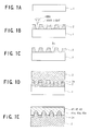
- Figs. 1A to 1E and Fig. 2 are schematic views illustrating a method for manufacturing an optical disc 100 according to an embodiment of the present invention and the structure thereof.
- the optical disc 100 is a reproduction-only multilayer optical disc having at least three information layers, in this embodiment, the optical disc 100 having a one-sided three layer structure will be described by way of example.
- Figs. 1A to 1E are schematic views showing steps of forming an original board and of injection molding a PC substrate. However, detailed steps, such as surface cleaning, which are performed whenever necessary during the above process, are omitted. In addition, although pit shapes recorded on the three information layers are actually different from each other depending on contents of the information, the pits having the same shape are shown in Figs. 1A to 1E and Fig. 2 .
- the information to be recorded on each layer is independently recorded on a resist 2 applied on a Si wafer 1 by an exposure apparatus ( Figs. 1A and 1B ).
- the Si wafer 1 thus exposed is immersed in an etching solution, and only exposed portions are dissolved out, thereby forming concave pits 2a ( Fig. 1C ).
- Ni-made stampers 3 having transferred convex pits 3a are formed (Fig. ID).
- Fig. ID three types of Ni-made stampers 3 are actually formed for the respective three information layers.
- Ni-made stampers 3 are sequentially set in an injection molding machine, and PC substrates 41, 42, and 43 are injection molded to have a predetermined thickness (for example, in the case of DVD, 0.6 mm) ( Fig. 1E ).
- the PC substrates 41, 42, and 43 have information for the first, the second, and the third layers, respectively.
- Concave pits 41a, 42a, and 43a for the respective layers are transferred on the PC substrates 41, 42, and 43, respectively.
- the optical disc 100 shown in Fig. 2 is composed of the first, the second, and the third layers provided in that order from the bottom and is sequentially formed from the first layer to the third layer.
- laser light is irradiated from the bottom side.
- a reflection layer 11 having a thickness determined by optical design is formed by sputtering, thereby forming the first layer.
- the PC substrate 42 on which the information for the second layer is recorded is pressed on the UV curable resin 12 so as to transfer the information.
- the PC substrate 42 is not used as a constituent element of the optical disc 100 but is used as a stamper for the UV curable resin 12.
- the information pits 41a of the first layer have a concave shape
- the convex pits 12a for the second layer are transferred on the UV curable resin 12.
- a reflection layer 13 of the embodiment according to the present invention is formed on the convex pits 12a described above. That is, the transmissive reflection layer 13 for the second layer (that is, the information layer other than the layers most close to and most far from the light incident layer) is formed by sputtering which has a thickness of 5 to 20 nm and which has a refractive index of 3.0 or more and an extinction coefficient of 0.6 or less with respect to a laser wavelength of a light source. The thickness is determined by optical calculation so as to satisfy necessary reflectance and transmission coefficient.
- the transmissive reflection layer 13 As a material for the transmissive reflection layer 13, at least one material selected from the group consisting of Si, a SiCr alloy, a SiNb alloy, a SiW alloy, and SiC is preferably used. In addition, a composite material containing at least one of Al and Ag and at least one of SiO 2 , Al 2 O 3 , Si 3 N 4 , and AlN is also preferably used. In addition, any other material may also be used as long as it has the optical constant described above.
- the material for the transmissive reflection layer a material primarily composed of Al or Ag has been used.
- the film forming rate of Al or Ag is fast, the precise thickness control is difficult to perform.
- the film forming rate of the material for the transmissive reflection layer 13 of the above embodiment is slow as compared to that of Al and Ag, and hence the thickness control can be easily performed.
- a thin film of a material primarily composed of Ag generally has a high internal stress.
- the reflection layer is formed on the resin layer 12 having the convex pits 12a as the second layer using a material primarily composed of Ag, the convex pits 12a disadvantageously tend to be crushed or deformed. In particular, this tendency becomes apparent for small pits such as 2T or 3T.
- the material for the transmissive reflection layer 13 of this embodiment has a low internal stress as compared to that of Ag, and the transmissive reflection layer 13 formed of the material described above does not crush nor deform the convex pits 12a transferred on the resin layer 12.
- the third layer which is the last layer, is separately formed by forming a total-reflection layer 15 on the PC substrate 43 which is formed beforehand so as to have the information pits 43a for the third layer.
- a UV curable resin 14 is applied on the reflection layer 13 formed for the second layer as described above, and the PC substrate 43 and the reflection layer 15, which are formed separately for the third layer, are adhered onto the resin 14 so that the reflection layer 15 is brought into contact therewith.
- the one-sided three layer optical disc 100 is formed.
- the optical disc 100 was actually formed based on the manufacturing steps described above, and the test results of its performance will be described.
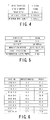
- Fig. 3 is a view showing the structure of the optical disc 100 manufactured as Example 1 of the present invention.
- a reflection layer 21 of Ag 98 Pd 1 Cu 1 (the number provided for the atomic symbol indicates an atomic ratio, and hereinafter, the number indicates the same as described above) having a thickness of 17 nm was formed on a 580- ⁇ m thick PC substrate 20 having concave information pits 20a, so that the first layer was formed. The time necessary for this film formation was 3 seconds.
- a UV curable resin 22 was applied to have a thickness of 15 ⁇ m using with a spin coater, and a PC substrate having information pits for the second layer was pressed on the UV curable resin 22, so that convex pits 22a were transferred on the resin 22. Subsequently, by irradiation of UV light, the UV curable resin 22 was cured.
- a film having a thickness of 12 nm was formed by a DC magnetron sputtering method using CrSi 2 as a raw material.
- the time necessary for this film formation was 8 seconds.
- a reflection layer 25 for the third layer was formed by a DC magnetron sputtering method to have a thickness of 100 nm on a 600- ⁇ m thick PC substrate 26 on which information for the third layer was recorded in the form of concave pits 26a.
- the time necessary for this film formation was 6 seconds.
- the reflection layer 25 thus formed was adhered to the PC substrate 20 formed beforehand, which was provided with the first layer and the second layer, with a UV curable resin 24 having a thickness of 20 ⁇ m interposed therebetween, thereby forming the optical disc 100 as the example.
- the other physical properties of the example are shown in the table of Fig. 4 .
- the optical disc 100 thus formed was evaluated under the conditions shown in the table of Fig. 5 .
- a PRSNR was used as the evaluation index.
- the PRSNR is an evaluation index for HD DVD standardized by a DVD forum and is an index which can express an S/N ratio of a reproduced signal and which can also simultaneously express an actual reproduced waveform and a theoretical PR waveform linearity. According to the standardization of a reproduction-only HD DVD (HD DVD-ROM), a PRSNR of 15 or more is required.
- the PRSNRs of the first, the second, and the third layers were 18, 18, and 21, respectively. All the results satisfied the standardization of 15 or more, and hence the effect of the material for the second layer of this example was apparently confirmed.
- Example 1 of the present invention a comparative one-sided three layer optical disc was formed which had the same structure as that in Example 1 except that the material for the reflection layer for the second layer was different.
- One disc A using Ag 98 Pd 1 Cu 1 (thickness: 17 nm) and 10 discs B using Ag 99 Mo 1 (thickness: 10 nm) as the material for the reflection layer for the second layer were formed.
- the discs described above were evaluated under the conditions shown in the table of Fig. 5 .
- the PNSNRs of the first, the second, and the third layers of the disc A were 18, 10, and 21, respectively, and hence, the second layer could not satisfy the standardization of 15 or more.
- symmetry S is an index represented by the following equation (1).
- S I ⁇ 2 ⁇ H + I ⁇ 2 ⁇ L / 2 - I ⁇ 11 ⁇ H + I ⁇ 11 ⁇ L / 2 / I ⁇ 11 ⁇ H - I ⁇ 11 ⁇ L
- the numerator of the equation (1) indicates the difference in central value of the amplitude between an 11T pit having a largest amplitude among reproduced signals and a 2T pit having a smallest amplitude.
- the denominator indicates the amplitude of the 11T pit.
- the intensity of the reproduced signal from the 2T pit was decreased, and as a result, it was believed that the central value of the 2T pit signal was deviated from that of the 11T pit signal.
- the evaluation results of the ten discs B are shown in the table of Fig. 6 .
- the reflectance of the disc B-3 and that of the disc B-8 were low as compared to those of the other discs, and the PRSNRs were also lower than the standardization thereof.
- the symmetries S of the 10 discs B were all within ⁇ 0.01, and hence it was confirmed that the symmetry S did not cause any problem.
- the variation in thickness was increased by the variation in sputtering time, the reflectance varied thereby, and as a result, the variation in properties occurred.
- the optical disc 100 having the same configuration as that of Example 1 except that NbSi 2 (thickness: 15 nm) was used as the material for the second layer was formed as Example 2 of the present invention.
- the optical disc 100 thus formed was evaluated under the conditions shown in the table of Fig. 5 as was the case described above.
- the PRSNRs of the first, the second, and the third layers were 19, 19, and 21, respectively, and all satisfied the standardization of 15 or more. Also from the results of Example 2, the effect of the material for the second layer of the present invention was apparently confirmed.
- the optical disc 100 having a superior PRSNR, which is used as the evaluation index can be provided.
- the stable optical disc 100 having a large manufacturing margin and high reproducibility can be provided.
- Fig. 7 is a schematic view showing the structure of an optical disc device 200 according to an embodiment of the present invention which reproduces the above one-sided multilayer optical disc 100.
- a semiconductor laser light source 120 having a short wavelength is used as a light source.
- the wavelength of light emitted from the source is, for example, a violet wavelength range from 400 to 410 nm.
- Light beams 102 emitted from the semiconductor laser light source 120 are made parallel by a collimate lens 121, then pass through a polarized beam splitter 122 and a ⁇ /4 plate 123, and are finally incident on an object lens 124. Subsequently, the beams pass the substrate of the optical disc 100 and then converge on the individual information layers.
- reflected light beams 101 by the information layers of the optical disc 100 again pass the substrate of the optical disc 100, then pass the object lens 124 and the ⁇ /4 plate 123, and are then reflected by the polarized beam splitter 122, the light beams 101 pass a condenser lens 125 and are then incident on a light detector 127.
- a light receiving portion of the light detector 127 is generally divided into a plurality of light receiving parts, and current in accordance with light intensity is output from each light receiving part.
- the current thus output is converted into a voltage by an I/V amplifier (current-voltage transformer), which is not shown, and is then input into an arithmetic circuit 140.
- An input voltage signal is arithmetically processed by the arithmetic circuit 140 into a tilt error signal, an RF signal, a focus error signal, a track error signal, and the like.
- the tilt error signal is used for tilt control
- the RF signal is used to reproduce information recorded on the optical disc 100
- the focus error signal is used for focus control
- the track error signal is used for tracking control.
- the object lens 124 can be driven by an actuator 128 in the top-down direction, the disc radial direction, and the tilt direction (radial direction or/and tangential direction) and is controlled by a servo driver 150 so as to follow information tracks on the optical disc 100.
- tilt directions there are two types of tilt directions. That is, there are a "radial tilt” generated when the disc surface tilts toward the center of the optical disc and a "tangential tilt” generated in the tangent line direction of the track. Of those described above, the radial tilt generally occurs in the disc. Besides the tilt generated during disc manufacturing, a tilt generated by long-term use and/or a tilt generated by a rapid change in use environment must also be taken into consideration.
- the present invention is not limited to the embodiments described above, and in an execution phase, the constituent elements may be variously change and modified without departing from the spirit and the scope of the present invention.
- various changes and modifications may also be made in accordance with the present invention.
- the constituent elements described in the embodiments some of them may be omitted.
- the constituent elements of the different embodiments may be used in combination.
Landscapes
- Optical Record Carriers And Manufacture Thereof (AREA)
Applications Claiming Priority (1)
| Application Number | Priority Date | Filing Date | Title |
|---|---|---|---|
| JP2006350272A JP2008159228A (ja) | 2006-12-26 | 2006-12-26 | 光ディスク及び光ディスク装置 |
Publications (2)
| Publication Number | Publication Date |
|---|---|
| EP1939872A2 true EP1939872A2 (de) | 2008-07-02 |
| EP1939872A3 EP1939872A3 (de) | 2008-08-06 |
Family
ID=39227435
Family Applications (1)
| Application Number | Title | Priority Date | Filing Date |
|---|---|---|---|
| EP07150023A Withdrawn EP1939872A3 (de) | 2006-12-26 | 2007-12-14 | Optische Platte und optisches Plattengerät |
Country Status (3)
| Country | Link |
|---|---|
| US (1) | US20080151728A1 (de) |
| EP (1) | EP1939872A3 (de) |
| JP (1) | JP2008159228A (de) |
Families Citing this family (2)
| Publication number | Priority date | Publication date | Assignee | Title |
|---|---|---|---|---|
| KR101442962B1 (ko) * | 2013-03-04 | 2014-09-23 | 주식회사 동부하이텍 | 이미지 센서 |
| TWI593290B (zh) | 2015-07-30 | 2017-07-21 | 力晶科技股份有限公司 | 影像感測器 |
Citations (1)
| Publication number | Priority date | Publication date | Assignee | Title |
|---|---|---|---|---|
| JP2002251801A (ja) | 2001-02-23 | 2002-09-06 | Sony Corp | ディスク状記録媒体の製造方法及び信号転写装置 |
Family Cites Families (4)
| Publication number | Priority date | Publication date | Assignee | Title |
|---|---|---|---|---|
| KR100402169B1 (ko) * | 1995-04-27 | 2004-03-10 | 닛폰콜롬비아 가부시키가이샤 | 다층구조광정보매체 |
| JP3867347B2 (ja) * | 1997-06-20 | 2007-01-10 | ソニー株式会社 | 多層光ディスク |
| JP2000298875A (ja) * | 1999-02-13 | 2000-10-24 | Sony Corp | 光記録媒体 |
| CN101138035A (zh) * | 2005-03-17 | 2008-03-05 | 株式会社理光 | 光学记录介质 |
-
2006
- 2006-12-26 JP JP2006350272A patent/JP2008159228A/ja active Pending
-
2007
- 2007-12-14 EP EP07150023A patent/EP1939872A3/de not_active Withdrawn
- 2007-12-19 US US11/960,383 patent/US20080151728A1/en not_active Abandoned
Patent Citations (1)
| Publication number | Priority date | Publication date | Assignee | Title |
|---|---|---|---|---|
| JP2002251801A (ja) | 2001-02-23 | 2002-09-06 | Sony Corp | ディスク状記録媒体の製造方法及び信号転写装置 |
Also Published As
| Publication number | Publication date |
|---|---|
| JP2008159228A (ja) | 2008-07-10 |
| EP1939872A3 (de) | 2008-08-06 |
| US20080151728A1 (en) | 2008-06-26 |
Similar Documents
| Publication | Publication Date | Title |
|---|---|---|
| KR100894972B1 (ko) | 광학 기록 매체 | |
| CN100533564C (zh) | 光记录与再现介质制造压模的制造方法 | |
| KR20000006538A (ko) | 광기록매체,광기록매체를이용한광기록및재생장치및광기록매체의제조방법 | |
| JPH11328732A (ja) | 光学情報記録媒体 | |
| US6934243B2 (en) | Optical information recording medium, recording/reproducing apparatus and recording /reproducing method for the same, and method for manufacturing optical information recording medium | |
| EP1178475A2 (de) | Optisches Aufzeichnungsmedium | |
| US20080151728A1 (en) | Optical disc and optical disc device | |
| US7567499B2 (en) | Optical disc and method of producing the same | |
| US7539121B2 (en) | Optical recording medium and process for producing the same | |
| KR20050074273A (ko) | 광디스크 제조용 원반의 제작 방법 및 광디스크의 제조 방법 | |
| US20040262793A1 (en) | Multi-layered optical recording medium and multi-layered optical recording medium manufacturing method | |
| US7619962B2 (en) | Optical disc and method of producing the same | |
| KR101058031B1 (ko) | 고밀도 기록 매체 형성 방법, 패턴 형성 방법 및 그 기록매체 | |
| JP4705530B2 (ja) | 光記録媒体とその基板、及び該基板の成形用スタンパ | |
| EP1898406A2 (de) | Optische Scheibe, optische Scheibenvorrichtung und Verfahren zur Wiedergabe einer optischen Scheibe | |
| US20050259562A1 (en) | Optical recording medium and production method thereof | |
| US20040241575A1 (en) | Optical disk and method and apparatus for manufacturing the same | |
| CN101714370B (zh) | 生产光盘的方法和生产压模的方法 | |
| US20060290018A1 (en) | Process for produicng stamper for direct mastering, and stamper produced by such process and optical disc | |
| KR20090115660A (ko) | 광 기록 매체 및 그의 제조 방법과, 스퍼터링용 타겟 및 그의 제조 방법 | |
| JP4604854B2 (ja) | 光記録媒体、光ディスク原盤およびその製造方法 | |
| US7082097B2 (en) | Optical disc capable of enhancing the performance of disc driver | |
| JP2010118114A (ja) | 光情報記録媒体 | |
| JP2005032317A (ja) | 光学記録再生媒体、光学記録再生媒体製造用スタンパ及び光学記録方法 | |
| JPH04263141A (ja) | 反射コート付きガラス原盤 |
Legal Events
| Date | Code | Title | Description |
|---|---|---|---|
| PUAI | Public reference made under article 153(3) epc to a published international application that has entered the european phase |
Free format text: ORIGINAL CODE: 0009012 |
|
| 17P | Request for examination filed |
Effective date: 20071214 |
|
| AK | Designated contracting states |
Kind code of ref document: A2 Designated state(s): AT BE BG CH CY CZ DE DK EE ES FI FR GB GR HU IE IS IT LI LT LU LV MC MT NL PL PT RO SE SI SK TR |
|
| AX | Request for extension of the european patent |
Extension state: AL BA HR MK RS |
|
| PUAL | Search report despatched |
Free format text: ORIGINAL CODE: 0009013 |
|
| AK | Designated contracting states |
Kind code of ref document: A3 Designated state(s): AT BE BG CH CY CZ DE DK EE ES FI FR GB GR HU IE IS IT LI LT LU LV MC MT NL PL PT RO SE SI SK TR |
|
| AX | Request for extension of the european patent |
Extension state: AL BA HR MK RS |
|
| RIC1 | Information provided on ipc code assigned before grant |
Ipc: G11B 7/258 20060101ALI20080627BHEP Ipc: G11B 7/24 20060101AFI20080404BHEP |
|
| 17Q | First examination report despatched |
Effective date: 20090309 |
|
| AKX | Designation fees paid |
Designated state(s): DE FR GB |
|
| STAA | Information on the status of an ep patent application or granted ep patent |
Free format text: STATUS: THE APPLICATION IS DEEMED TO BE WITHDRAWN |
|
| 18D | Application deemed to be withdrawn |
Effective date: 20090721 |