EP1913445B1 - Abbildungssystem, insbesondere projektionsobjektiv einer mikrolithographischen projektionsbelichtungsanlage - Google Patents
Abbildungssystem, insbesondere projektionsobjektiv einer mikrolithographischen projektionsbelichtungsanlage Download PDFInfo
- Publication number
- EP1913445B1 EP1913445B1 EP06778169A EP06778169A EP1913445B1 EP 1913445 B1 EP1913445 B1 EP 1913445B1 EP 06778169 A EP06778169 A EP 06778169A EP 06778169 A EP06778169 A EP 06778169A EP 1913445 B1 EP1913445 B1 EP 1913445B1
- Authority
- EP
- European Patent Office
- Prior art keywords
- imaging system
- refractive index
- cubic
- crystalline material
- numerical aperture
- Prior art date
- Legal status (The legal status is an assumption and is not a legal conclusion. Google has not performed a legal analysis and makes no representation as to the accuracy of the status listed.)
- Not-in-force
Links
- 238000003384 imaging method Methods 0.000 title claims description 43
- 230000003287 optical effect Effects 0.000 claims abstract description 26
- 239000002178 crystalline material Substances 0.000 claims abstract description 11
- 239000000463 material Substances 0.000 claims description 39
- VYPSYNLAJGMNEJ-UHFFFAOYSA-N silicon dioxide Inorganic materials O=[Si]=O VYPSYNLAJGMNEJ-UHFFFAOYSA-N 0.000 claims description 9
- 229910052596 spinel Inorganic materials 0.000 claims description 6
- FYYHWMGAXLPEAU-UHFFFAOYSA-N Magnesium Chemical compound [Mg] FYYHWMGAXLPEAU-UHFFFAOYSA-N 0.000 claims description 5
- 239000011575 calcium Substances 0.000 claims description 5
- 239000011777 magnesium Substances 0.000 claims description 5
- 229910052749 magnesium Inorganic materials 0.000 claims description 5
- 239000000395 magnesium oxide Substances 0.000 claims description 5
- CPLXHLVBOLITMK-UHFFFAOYSA-N magnesium oxide Inorganic materials [Mg]=O CPLXHLVBOLITMK-UHFFFAOYSA-N 0.000 claims description 5
- 239000011029 spinel Substances 0.000 claims description 5
- AXZKOIWUVFPNLO-UHFFFAOYSA-N magnesium;oxygen(2-) Chemical compound [O-2].[Mg+2] AXZKOIWUVFPNLO-UHFFFAOYSA-N 0.000 claims description 4
- 239000000377 silicon dioxide Substances 0.000 claims description 4
- -1 CaNa4Si3O9 Inorganic materials 0.000 claims description 3
- ODINCKMPIJJUCX-UHFFFAOYSA-N calcium oxide Inorganic materials [Ca]=O ODINCKMPIJJUCX-UHFFFAOYSA-N 0.000 claims description 3
- TWNQGVIAIRXVLR-UHFFFAOYSA-N oxo(oxoalumanyloxy)alumane Chemical compound O=[Al]O[Al]=O TWNQGVIAIRXVLR-UHFFFAOYSA-N 0.000 claims description 3
- 239000000758 substrate Substances 0.000 claims description 3
- 229910019901 yttrium aluminum garnet Inorganic materials 0.000 claims description 3
- OYPRJOBELJOOCE-UHFFFAOYSA-N Calcium Chemical compound [Ca] OYPRJOBELJOOCE-UHFFFAOYSA-N 0.000 claims description 2
- DGAQECJNVWCQMB-PUAWFVPOSA-M Ilexoside XXIX Chemical compound C[C@@H]1CC[C@@]2(CC[C@@]3(C(=CC[C@H]4[C@]3(CC[C@@H]5[C@@]4(CC[C@@H](C5(C)C)OS(=O)(=O)[O-])C)C)[C@@H]2[C@]1(C)O)C)C(=O)O[C@H]6[C@@H]([C@H]([C@@H]([C@H](O6)CO)O)O)O.[Na+] DGAQECJNVWCQMB-PUAWFVPOSA-M 0.000 claims description 2
- JNDMLEXHDPKVFC-UHFFFAOYSA-N aluminum;oxygen(2-);yttrium(3+) Chemical compound [O-2].[O-2].[O-2].[Al+3].[Y+3] JNDMLEXHDPKVFC-UHFFFAOYSA-N 0.000 claims description 2
- BRPQOXSCLDDYGP-UHFFFAOYSA-N calcium oxide Chemical compound [O-2].[Ca+2] BRPQOXSCLDDYGP-UHFFFAOYSA-N 0.000 claims description 2
- 239000000292 calcium oxide Substances 0.000 claims description 2
- 239000002223 garnet Substances 0.000 claims description 2
- 238000004519 manufacturing process Methods 0.000 claims description 2
- 238000000034 method Methods 0.000 claims description 2
- 229910001950 potassium oxide Inorganic materials 0.000 claims description 2
- 239000011734 sodium Substances 0.000 claims description 2
- PNEYBMLMFCGWSK-UHFFFAOYSA-N aluminium oxide Inorganic materials [O-2].[O-2].[O-2].[Al+3].[Al+3] PNEYBMLMFCGWSK-UHFFFAOYSA-N 0.000 claims 5
- 229910052593 corundum Inorganic materials 0.000 claims 5
- 229910001845 yogo sapphire Inorganic materials 0.000 claims 5
- 229910052681 coesite Inorganic materials 0.000 claims 3
- 229910052906 cristobalite Inorganic materials 0.000 claims 3
- 229910052682 stishovite Inorganic materials 0.000 claims 3
- 229910052905 tridymite Inorganic materials 0.000 claims 3
- 239000011248 coating agent Substances 0.000 claims 2
- 238000000576 coating method Methods 0.000 claims 2
- CHWRSCGUEQEHOH-UHFFFAOYSA-N potassium oxide Chemical compound [O-2].[K+].[K+] CHWRSCGUEQEHOH-UHFFFAOYSA-N 0.000 claims 2
- 229910026161 MgAl2O4 Inorganic materials 0.000 claims 1
- 229910052909 inorganic silicate Inorganic materials 0.000 claims 1
- 229910052814 silicon oxide Inorganic materials 0.000 claims 1
- 229910001948 sodium oxide Inorganic materials 0.000 claims 1
- DHEQXMRUPNDRPG-UHFFFAOYSA-N strontium nitrate Inorganic materials [Sr+2].[O-][N+]([O-])=O.[O-][N+]([O-])=O DHEQXMRUPNDRPG-UHFFFAOYSA-N 0.000 claims 1
- 239000013078 crystal Substances 0.000 description 32
- 229910018072 Al 2 O 3 Inorganic materials 0.000 description 10
- 229910004298 SiO 2 Inorganic materials 0.000 description 5
- 238000010521 absorption reaction Methods 0.000 description 4
- 238000005286 illumination Methods 0.000 description 4
- 230000004075 alteration Effects 0.000 description 3
- 238000012937 correction Methods 0.000 description 3
- 238000001393 microlithography Methods 0.000 description 3
- KRHYYFGTRYWZRS-UHFFFAOYSA-M Fluoride anion Chemical compound [F-] KRHYYFGTRYWZRS-UHFFFAOYSA-M 0.000 description 2
- 229910004283 SiO 4 Inorganic materials 0.000 description 2
- 230000003247 decreasing effect Effects 0.000 description 2
- 230000000694 effects Effects 0.000 description 2
- 229910020068 MgAl Inorganic materials 0.000 description 1
- ZLMJMSJWJFRBEC-UHFFFAOYSA-N Potassium Chemical compound [K] ZLMJMSJWJFRBEC-UHFFFAOYSA-N 0.000 description 1
- 238000013459 approach Methods 0.000 description 1
- 230000005540 biological transmission Effects 0.000 description 1
- 229910052791 calcium Inorganic materials 0.000 description 1
- 238000010276 construction Methods 0.000 description 1
- 230000001419 dependent effect Effects 0.000 description 1
- 238000013461 design Methods 0.000 description 1
- 238000007654 immersion Methods 0.000 description 1
- 238000005259 measurement Methods 0.000 description 1
- 231100000252 nontoxic Toxicity 0.000 description 1
- 230000003000 nontoxic effect Effects 0.000 description 1
- 238000012634 optical imaging Methods 0.000 description 1
- 239000011591 potassium Substances 0.000 description 1
- 239000010453 quartz Substances 0.000 description 1
- 229910052594 sapphire Inorganic materials 0.000 description 1
- 239000010980 sapphire Substances 0.000 description 1
- 229910052708 sodium Inorganic materials 0.000 description 1
- 239000013589 supplement Substances 0.000 description 1
- 239000012780 transparent material Substances 0.000 description 1
Images
Classifications
-
- G—PHYSICS
- G02—OPTICS
- G02B—OPTICAL ELEMENTS, SYSTEMS OR APPARATUS
- G02B1/00—Optical elements characterised by the material of which they are made; Optical coatings for optical elements
- G02B1/02—Optical elements characterised by the material of which they are made; Optical coatings for optical elements made of crystals, e.g. rock-salt, semi-conductors
-
- G—PHYSICS
- G03—PHOTOGRAPHY; CINEMATOGRAPHY; ANALOGOUS TECHNIQUES USING WAVES OTHER THAN OPTICAL WAVES; ELECTROGRAPHY; HOLOGRAPHY
- G03F—PHOTOMECHANICAL PRODUCTION OF TEXTURED OR PATTERNED SURFACES, e.g. FOR PRINTING, FOR PROCESSING OF SEMICONDUCTOR DEVICES; MATERIALS THEREFOR; ORIGINALS THEREFOR; APPARATUS SPECIALLY ADAPTED THEREFOR
- G03F7/00—Photomechanical, e.g. photolithographic, production of textured or patterned surfaces, e.g. printing surfaces; Materials therefor, e.g. comprising photoresists; Apparatus specially adapted therefor
- G03F7/70—Microphotolithographic exposure; Apparatus therefor
- G03F7/70216—Mask projection systems
- G03F7/70341—Details of immersion lithography aspects, e.g. exposure media or control of immersion liquid supply
-
- G—PHYSICS
- G03—PHOTOGRAPHY; CINEMATOGRAPHY; ANALOGOUS TECHNIQUES USING WAVES OTHER THAN OPTICAL WAVES; ELECTROGRAPHY; HOLOGRAPHY
- G03F—PHOTOMECHANICAL PRODUCTION OF TEXTURED OR PATTERNED SURFACES, e.g. FOR PRINTING, FOR PROCESSING OF SEMICONDUCTOR DEVICES; MATERIALS THEREFOR; ORIGINALS THEREFOR; APPARATUS SPECIALLY ADAPTED THEREFOR
- G03F7/00—Photomechanical, e.g. photolithographic, production of textured or patterned surfaces, e.g. printing surfaces; Materials therefor, e.g. comprising photoresists; Apparatus specially adapted therefor
- G03F7/70—Microphotolithographic exposure; Apparatus therefor
- G03F7/708—Construction of apparatus, e.g. environment aspects, hygiene aspects or materials
- G03F7/7095—Materials, e.g. materials for housing, stage or other support having particular properties, e.g. weight, strength, conductivity, thermal expansion coefficient
- G03F7/70958—Optical materials or coatings, e.g. with particular transmittance, reflectance or anti-reflection properties
- G03F7/70966—Birefringence
Definitions
- the invention relates to an imaging system, in particular a projection objective of a microlithographic projection exposure apparatus.
- the invention relates to a projection lens which allows the use of high-index crystal materials while limiting the negative impact of intrinsic birefringence on the imaging properties.
- a "refractive index” is referred to as "high” if its value at the given wavelength exceeds that of quartz, with a value of about 1.56 at a wavelength of 193 nm.
- refractive index at DUV and VUV wavelengths ( ⁇ 250nm) larger is about 1.6, for example, magnesium spinel having a refractive index of about 1.87 at a wavelength of 193 nm, or magnesium oxide whose refractive index at 193 nm is about 2.0.
- a problem with using these materials as lens elements is that they have intrinsic birefringence due to their cubic crystal structure, which increases with low wavelength, e.g. Measurements of the IDB-induced delay for magnesium spinel at a wavelength of 193 nm have given a value of 52 nm / cm, and the IDB-induced delay for magnesium oxide at 193 nm was estimated to be about 72 nm / cm. Depending on the design conditions, such a delay can lead to lateral beam deviations in the image field which are 3 to 5 times the pattern width to be imaged.
- a projection lens with a last optical element made of a material with a high refractive index (n ⁇ 1.6), in particular sapphire, and typical numerical apertures greater than 1.35 is known.
- the object of the present invention is to provide an imaging system, in particular a projection objective of a microlithographic projection exposure apparatus, which enables the use of high-index crystal materials while limiting the negative influence of intrinsic birefringence.
- an imaging system in particular a projection objective of a microlithographic projection exposure apparatus, comprises at least one optical element which is a cubic crystal material which has a refractive index n greater than 1.6 at a given operating wavelength, and has an image-side numerical aperture NA which is smaller than the refractive index n, the difference (n-NA) between the refractive index n and the numerical aperture NA of the imaging system maximum is 0.2.
- the invention is initially based on the recognition that the effect of intrinsic birefringence does not increase linearly with shorter wavelength, but rather begins gradually and then increases dramatically with decreasing wavelength. This non-linearity is all the more pronounced as the respective working wavelength approaches the absorption edge (in the UV range) for the material in question.
- the potential of materials with the highest possible refractive indexes is not exhausted, but the refractive index is just as high (and not higher) chosen, as it is necessary to geometrically coupled projection light even at the maximum beam angles through the projection lens and Picture to bring.
- the more moderate requirement for the height of the refractive index is exploited in order to select such a crystal material whose absorption edge lies deeper in the UV, as a result of which the intrinsic birefringence in the working wavelength has increased even smaller or less than in the case of a material with higher absorption edge is the case.
- NA 1.5
- the distance of the refractive index n to lower (lower) image-side numerical aperture of the imaging system lower is, but still just sufficient to couple the projection light even at maximum beam angles still through the imaging system or bring to imaging.
- an imaging system in particular a projection objective of a microlithographic projection exposure apparatus, comprises at least one optical element which has a cubic crystal material which has a refractive index n at a predetermined operating wavelength and has a numerical aperture NA which is smaller than the refractive index n is, of at least 1.50, wherein the difference (n-NA) between the refractive index n and the numerical aperture NA of the imaging system is at most 0.2.
- the difference (n-NA) between the refractive index n of the optical element and the numerical aperture NA of the imaging system is in the range of 0.05 to 0.20, preferably in the range of 0.05 to 0.15, and more preferably in the range of 0.05 to 0.10.
- a limitation of the intrinsic birefringence is achieved by the upper limit of the refractive index as stated above, while limiting the total lens volume of the projection lens is achieved by the lower limit of the refractive index.
- materials used according to the invention preferably to be met criteria are sufficient Stability to humidity and UV light, high hardness and good optical workability, as well as non-toxic components.
- the cubic crystal material has an oxide, for which a sufficient transmission at a comparatively high refractive index was obtained.
- the cubic crystal material comprises sapphire (Al 2 O 3 ) and a potassium or calcium oxide.
- the cubic crystal material is preferably at least one material which is selected from the group 7Al 2 O 3 ⁇ 12CaO, Al 2 O 3 ⁇ K 2 O, Al 2 O 3 ⁇ 3CaO, Al 2 O 3 ⁇ SiO KO , Al 2 O 3 -SiO 2 ⁇ 2K and Al 2 O 3 ⁇ 3CaO6H 2 O.
- the proportion of sapphire causes a widening of the band gap or a shift of the absorption edge in the UV range while increasing the refractive index, so that additional refractive index components supplement the mixed crystal, resulting in the above reduction of intrinsic birefringence leads.
- the cubic crystal material comprises calcium, sodium and silica.
- the cubic crystal material preferably comprises at least one material selected from the group consisting of CaNa 2 SiO 4 and CaNa 4 Si 3 O 9 .
- the cubic crystal material comprises at least one material from the group which Sr (NO 3) 2, MgONa 2 O ⁇ SiO 2 and Ca (NO 3) 2 contains.
- the optical element is preferably the image-side last refractive lens of the imaging system.
- the optical element is composed of a first partial element with refractive power and a second, substantially non-frictional partial element.
- the first subelement is preferably a substantially plano-convex lens
- the second subelement is a plane-parallel plate.
- Such a construction of the optical element has the advantage of a particularly effective correction of the spherical aberration, which is typically the largest contribution to aberrations to be handled at high apertures.
- a correction of the spherical aberration which is uniform over the image field can advantageously be achieved, in particular by the plane-parallel subelement.
- the second material is selected from the group of magnesium spinel (MgAl 2 O 4 ), yttrium aluminum garnet (Y 3 Al 5 O 12 ), MgO and scandium aluminum garnet (Sc 3 Al 5 O 12 ).
- the second subelement has an element axis and at least two subregions which have the same crystal section and are arranged rotated relative to one another around the element axis.
- the invention further relates to a microlithographic projection exposure apparatus and to a method for producing microlithographic components.
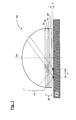
- Fig. 1 only schematically shows the structure of an optical element 100 in an imaging system according to the invention.
- the optical element 100 is preferably in particular the last image-side lens in a microlithographic projection objective whose fundamental structure is still described with reference to FIG Fig. 2 is explained.
- the optical element 100 is constructed from a first subelement 10 in the form of a plano-convex lens and a second subelement 20 in the form of a plane-parallel plate, wherein the light entry surface of the second subelement 20 is arranged directly adjacent to the light exit surface of the first subelement 10 and is preferably exploded thereon ,
- FIG. 1 The structure of the second partial element 20 from a total of four partial regions in the form of plane-parallel partial plates 21, 22, 23 and 24 is shown schematically.
- the second partial element 20 has a total of two partial regions, which have the same crystal section and are arranged rotated relative to one another around the element axis.
- the first sub-element 10 is made of a cubic crystalline material having such a refractive index, which is chosen in dependence on the numerical aperture NA of the imaging system so that the difference (n-NA) between this refractive index n and the numerical aperture NA of the imaging system maximum 0.2.
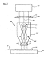
- a projection exposure apparatus 200 has an illumination device 201 and a projection objective 202.
- the projection objective 202 comprises a lens arrangement 203 with an aperture diaphragm AP, wherein an optical axis OA is defined by the lens arrangement 203, which is only schematically indicated.
- a mask 204 is arranged, which is held by means of a mask holder 205 in the beam path.
- Such masks 204 used in microlithography have a structure in the micrometer to nanometer range, which by means of the projection objective 202, for example reduced by a factor of 4 or 5 is reduced to an image plane IP.
- a photosensitive substrate 206, or a wafer, positioned by a substrate holder 207 is held.
- the still resolvable minimum structures depend on the wavelength ⁇ of the light used for the illumination as well as on the image-side numerical aperture of the projection lens 202, the maximum achievable resolution of the projection exposure apparatus 200 with decreasing wavelength ⁇ of the illumination device 201 and with increasing image-side numerical aperture of the projection lens 202 goes up.
- the projection lens 202 is configured as an imaging system according to the present invention.
- Fig. 2 is only schematically a possible, approximate position of an optical element 100 according to the invention indicated by dashed lines, wherein the optical element is arranged here according to a preferred embodiment, the image last optical element of the projection lens 202 and thus in the region of relatively high aperture angle.
- the optical element has the basis of Fig. 1 explained structure and is thus constructed in particular of a first sub-element 10 in the form of a plano-convex lens and a second sub-element 20 in the form of a plane-parallel plate according to the embodiments described above.
Landscapes
- Physics & Mathematics (AREA)
- General Physics & Mathematics (AREA)
- Health & Medical Sciences (AREA)
- Engineering & Computer Science (AREA)
- Environmental & Geological Engineering (AREA)
- Epidemiology (AREA)
- Public Health (AREA)
- Chemical & Material Sciences (AREA)
- Crystallography & Structural Chemistry (AREA)
- Optics & Photonics (AREA)
- Lenses (AREA)
Applications Claiming Priority (2)
| Application Number | Priority Date | Filing Date | Title |
|---|---|---|---|
| US70690305P | 2005-08-10 | 2005-08-10 | |
| PCT/EP2006/065070 WO2007017473A1 (de) | 2005-08-10 | 2006-08-04 | Abbildungssystem, insbesondere projektionsobjektiv einer mikrolithographischen projektionsbelichtungsanlage |
Publications (2)
| Publication Number | Publication Date |
|---|---|
| EP1913445A1 EP1913445A1 (de) | 2008-04-23 |
| EP1913445B1 true EP1913445B1 (de) | 2011-05-25 |
Family
ID=37188852
Family Applications (1)
| Application Number | Title | Priority Date | Filing Date |
|---|---|---|---|
| EP06778169A Not-in-force EP1913445B1 (de) | 2005-08-10 | 2006-08-04 | Abbildungssystem, insbesondere projektionsobjektiv einer mikrolithographischen projektionsbelichtungsanlage |
Country Status (7)
| Country | Link |
|---|---|
| US (1) | US20080182210A1 (enExample) |
| EP (1) | EP1913445B1 (enExample) |
| JP (1) | JP2009505124A (enExample) |
| KR (1) | KR20080028429A (enExample) |
| CN (1) | CN101243359B (enExample) |
| AT (1) | ATE511124T1 (enExample) |
| WO (1) | WO2007017473A1 (enExample) |
Families Citing this family (2)
| Publication number | Priority date | Publication date | Assignee | Title |
|---|---|---|---|---|
| DE102008001800A1 (de) * | 2007-05-25 | 2008-11-27 | Carl Zeiss Smt Ag | Projektionsobjektiv für die Mikrolithographie, Mikrolithographie-Projektionsbelichtungsanlage mit einem derartigen Projektionsobjektiv, mikrolithographisches Herstellungsverfahren für Bauelemente sowie mit diesem Verfahren hergestelltes Bauelement |
| CN114326075B (zh) * | 2021-12-10 | 2023-12-19 | 肯维捷斯(武汉)科技有限公司 | 一种生物样品的数字显微成像系统及镜检方法 |
Family Cites Families (12)
| Publication number | Priority date | Publication date | Assignee | Title |
|---|---|---|---|---|
| KR20000034967A (ko) * | 1998-11-30 | 2000-06-26 | 헨켈 카르스텐 | 수정-렌즈를 갖는 오브젝티브 및 투사 조명 장치 |
| US6995930B2 (en) * | 1999-12-29 | 2006-02-07 | Carl Zeiss Smt Ag | Catadioptric projection objective with geometric beam splitting |
| JP2004526331A (ja) * | 2001-05-15 | 2004-08-26 | カール・ツアイス・エスエムテイ・アーゲー | フッ化物結晶レンズを含む対物レンズ |
| JP2003021619A (ja) * | 2001-07-05 | 2003-01-24 | Canon Inc | 蛍石及びその分析法、製造法、光学特性評価法 |
| JPWO2003009015A1 (ja) * | 2001-07-18 | 2004-11-11 | 株式会社ニコン | フッ化ランタン膜を備えた光学素子 |
| US7092069B2 (en) * | 2002-03-08 | 2006-08-15 | Carl Zeiss Smt Ag | Projection exposure method and projection exposure system |
| JP2005537512A (ja) * | 2002-09-03 | 2005-12-08 | カール・ツアイス・エスエムテイ・アーゲー | 複屈折レンズを伴う対物レンズ |
| KR101211451B1 (ko) * | 2003-07-09 | 2012-12-12 | 가부시키가이샤 니콘 | 노광 장치 및 디바이스 제조 방법 |
| EP1697798A2 (en) | 2003-12-15 | 2006-09-06 | Carl Zeiss SMT AG | Projection objective having a high aperture and a planar end surface |
| US7466489B2 (en) * | 2003-12-15 | 2008-12-16 | Susanne Beder | Projection objective having a high aperture and a planar end surface |
| WO2005059645A2 (en) * | 2003-12-19 | 2005-06-30 | Carl Zeiss Smt Ag | Microlithography projection objective with crystal elements |
| JP2006113533A (ja) * | 2004-08-03 | 2006-04-27 | Nikon Corp | 投影光学系、露光装置、および露光方法 |
-
2006
- 2006-08-04 JP JP2008525556A patent/JP2009505124A/ja active Pending
- 2006-08-04 AT AT06778169T patent/ATE511124T1/de active
- 2006-08-04 EP EP06778169A patent/EP1913445B1/de not_active Not-in-force
- 2006-08-04 WO PCT/EP2006/065070 patent/WO2007017473A1/de not_active Ceased
- 2006-08-04 CN CN2006800296095A patent/CN101243359B/zh not_active Expired - Fee Related
- 2006-08-04 KR KR1020087001045A patent/KR20080028429A/ko not_active Ceased
-
2008
- 2008-02-07 US US12/027,731 patent/US20080182210A1/en not_active Abandoned
Also Published As
| Publication number | Publication date |
|---|---|
| CN101243359B (zh) | 2011-04-06 |
| KR20080028429A (ko) | 2008-03-31 |
| EP1913445A1 (de) | 2008-04-23 |
| JP2009505124A (ja) | 2009-02-05 |
| US20080182210A1 (en) | 2008-07-31 |
| WO2007017473A1 (de) | 2007-02-15 |
| CN101243359A (zh) | 2008-08-13 |
| ATE511124T1 (de) | 2011-06-15 |
Similar Documents
| Publication | Publication Date | Title |
|---|---|---|
| EP1122608B1 (de) | Projektionsbelichtungsanlage mit reflektivem Retikel | |
| EP1260845A2 (de) | Katadioptrisches Reduktionsobjektiv | |
| DE19902336A1 (de) | Optisches Projektionssystem und dieses verwendende Belichtungsvorrichtung und Belichtungsverfahren | |
| DE10133841A1 (de) | Objektiv mit Kristall-Linsen | |
| DE3439297C2 (de) | Spiegellinsenobjektiv | |
| EP1282011A2 (de) | Reflektives Projektionsobjektiv für EUV-Photolithographie | |
| DE102008007449A1 (de) | Beleuchtungsoptik zur Beleuchtung eines Objektfeldes einer Projektionsbelichtungsanlage für die Mikrolithographie | |
| WO2000070407A1 (de) | Projektionsobjektiv für die mikrolithographie | |
| DE19833481A1 (de) | Optisches Projektionssystem, dieses verwendende Belichtungsvorrichtung und Belichtungsverfahren | |
| DE102013008814A1 (de) | Großformatige katadioptrische Einheitsvergrößerungsoptiken für die Mikrolithographie | |
| DE102008040613A1 (de) | Optisches System einer mikrolithographischen Projektionsbelichtungsanlage | |
| EP1102100A2 (de) | Katadioptrisches Objektiv mit physikalischem Strahlteiler | |
| DE102016205619A1 (de) | Abschwächungsfilter für Projektionsobjektiv, Projektionsobjektiv mit Abschwächungsfilter für Projektionsbelichtungsanlage und Projektionsbelichtungsanlage mit Projektionsobjektiv | |
| DE102022205700A1 (de) | Projektionsobjektiv, Projektionsbelichtungsanlage und Projektionsbelichtungsverfahren | |
| DE102017207582A1 (de) | Projektionsobjektiv, Projektionsbelichtungsanlage und Projektionsbelichtungsverfahren | |
| EP1913445B1 (de) | Abbildungssystem, insbesondere projektionsobjektiv einer mikrolithographischen projektionsbelichtungsanlage | |
| DE102005024290A1 (de) | Abbildungssystem, insbesondere für eine mikrolithographische Projektionsbelichtungsanlage | |
| DE102006013560A1 (de) | Projektionsobjektiv einer mikrolithographischen Projektionsbelichtungsanlage sowie Verfahren zu dessen Herstellung | |
| DE102006038454A1 (de) | Projektionsobjektiv einer mikrolithographischen Projektionsbelichtungsanlage | |
| DE102006025044A1 (de) | Abbildungssystem, insbesondere Projektionsobjektiv einer mikrolithographischen Projektionsbelichtungsanlage | |
| DE102008054737A1 (de) | Mikrolithographische Projektionsbelichtungsanlage sowie Objektiv hierfür | |
| DE102005027099A1 (de) | Immersionslithographieobjektiv | |
| DE10224361A1 (de) | Projektionsobjektiv höchster Apertur | |
| DE102006028242A1 (de) | Projektionsobjektiv einer mikrolithographischen Projektionsbelichtungsanlage | |
| DE102022201001A1 (de) | Projektionsobjektiv, Projektionsbelichtungsanlage und Projektionsbelichtungsverfahren |
Legal Events
| Date | Code | Title | Description |
|---|---|---|---|
| PUAI | Public reference made under article 153(3) epc to a published international application that has entered the european phase |
Free format text: ORIGINAL CODE: 0009012 |
|
| 17P | Request for examination filed |
Effective date: 20080205 |
|
| AK | Designated contracting states |
Kind code of ref document: A1 Designated state(s): AT BE BG CH CY CZ DE DK EE ES FI FR GB GR HU IE IS IT LI LT LU LV MC NL PL PT RO SE SI SK TR |
|
| 17Q | First examination report despatched |
Effective date: 20100823 |
|
| GRAP | Despatch of communication of intention to grant a patent |
Free format text: ORIGINAL CODE: EPIDOSNIGR1 |
|
| DAX | Request for extension of the european patent (deleted) | ||
| RAP1 | Party data changed (applicant data changed or rights of an application transferred) |
Owner name: CARL ZEISS SMT GMBH |
|
| GRAS | Grant fee paid |
Free format text: ORIGINAL CODE: EPIDOSNIGR3 |
|
| GRAA | (expected) grant |
Free format text: ORIGINAL CODE: 0009210 |
|
| AK | Designated contracting states |
Kind code of ref document: B1 Designated state(s): AT BE BG CH CY CZ DE DK EE ES FI FR GB GR HU IE IS IT LI LT LU LV MC NL PL PT RO SE SI SK TR |
|
| REG | Reference to a national code |
Ref country code: GB Ref legal event code: FG4D Free format text: NOT ENGLISH |
|
| REG | Reference to a national code |
Ref country code: CH Ref legal event code: EP |
|
| REG | Reference to a national code |
Ref country code: IE Ref legal event code: FG4D Free format text: LANGUAGE OF EP DOCUMENT: GERMAN |
|
| REG | Reference to a national code |
Ref country code: DE Ref legal event code: R096 Ref document number: 502006009577 Country of ref document: DE Effective date: 20110707 |
|
| REG | Reference to a national code |
Ref country code: NL Ref legal event code: VDEP Effective date: 20110525 |
|
| PG25 | Lapsed in a contracting state [announced via postgrant information from national office to epo] |
Ref country code: SE Free format text: LAPSE BECAUSE OF FAILURE TO SUBMIT A TRANSLATION OF THE DESCRIPTION OR TO PAY THE FEE WITHIN THE PRESCRIBED TIME-LIMIT Effective date: 20110525 Ref country code: LT Free format text: LAPSE BECAUSE OF FAILURE TO SUBMIT A TRANSLATION OF THE DESCRIPTION OR TO PAY THE FEE WITHIN THE PRESCRIBED TIME-LIMIT Effective date: 20110525 Ref country code: PT Free format text: LAPSE BECAUSE OF FAILURE TO SUBMIT A TRANSLATION OF THE DESCRIPTION OR TO PAY THE FEE WITHIN THE PRESCRIBED TIME-LIMIT Effective date: 20110926 |
|
| PG25 | Lapsed in a contracting state [announced via postgrant information from national office to epo] |
Ref country code: GR Free format text: LAPSE BECAUSE OF FAILURE TO SUBMIT A TRANSLATION OF THE DESCRIPTION OR TO PAY THE FEE WITHIN THE PRESCRIBED TIME-LIMIT Effective date: 20110826 Ref country code: ES Free format text: LAPSE BECAUSE OF FAILURE TO SUBMIT A TRANSLATION OF THE DESCRIPTION OR TO PAY THE FEE WITHIN THE PRESCRIBED TIME-LIMIT Effective date: 20110905 Ref country code: IS Free format text: LAPSE BECAUSE OF FAILURE TO SUBMIT A TRANSLATION OF THE DESCRIPTION OR TO PAY THE FEE WITHIN THE PRESCRIBED TIME-LIMIT Effective date: 20110925 Ref country code: FI Free format text: LAPSE BECAUSE OF FAILURE TO SUBMIT A TRANSLATION OF THE DESCRIPTION OR TO PAY THE FEE WITHIN THE PRESCRIBED TIME-LIMIT Effective date: 20110525 Ref country code: SI Free format text: LAPSE BECAUSE OF FAILURE TO SUBMIT A TRANSLATION OF THE DESCRIPTION OR TO PAY THE FEE WITHIN THE PRESCRIBED TIME-LIMIT Effective date: 20110525 Ref country code: LV Free format text: LAPSE BECAUSE OF FAILURE TO SUBMIT A TRANSLATION OF THE DESCRIPTION OR TO PAY THE FEE WITHIN THE PRESCRIBED TIME-LIMIT Effective date: 20110525 Ref country code: CY Free format text: LAPSE BECAUSE OF FAILURE TO SUBMIT A TRANSLATION OF THE DESCRIPTION OR TO PAY THE FEE WITHIN THE PRESCRIBED TIME-LIMIT Effective date: 20110525 |
|
| REG | Reference to a national code |
Ref country code: IE Ref legal event code: FD4D |
|
| PG25 | Lapsed in a contracting state [announced via postgrant information from national office to epo] |
Ref country code: NL Free format text: LAPSE BECAUSE OF FAILURE TO SUBMIT A TRANSLATION OF THE DESCRIPTION OR TO PAY THE FEE WITHIN THE PRESCRIBED TIME-LIMIT Effective date: 20110525 |
|
| PG25 | Lapsed in a contracting state [announced via postgrant information from national office to epo] |
Ref country code: CZ Free format text: LAPSE BECAUSE OF FAILURE TO SUBMIT A TRANSLATION OF THE DESCRIPTION OR TO PAY THE FEE WITHIN THE PRESCRIBED TIME-LIMIT Effective date: 20110525 Ref country code: EE Free format text: LAPSE BECAUSE OF FAILURE TO SUBMIT A TRANSLATION OF THE DESCRIPTION OR TO PAY THE FEE WITHIN THE PRESCRIBED TIME-LIMIT Effective date: 20110525 Ref country code: IE Free format text: LAPSE BECAUSE OF FAILURE TO SUBMIT A TRANSLATION OF THE DESCRIPTION OR TO PAY THE FEE WITHIN THE PRESCRIBED TIME-LIMIT Effective date: 20110525 |
|
| BERE | Be: lapsed |
Owner name: CARL ZEISS SMT G.M.B.H. Effective date: 20110831 |
|
| PG25 | Lapsed in a contracting state [announced via postgrant information from national office to epo] |
Ref country code: RO Free format text: LAPSE BECAUSE OF FAILURE TO SUBMIT A TRANSLATION OF THE DESCRIPTION OR TO PAY THE FEE WITHIN THE PRESCRIBED TIME-LIMIT Effective date: 20110525 Ref country code: DK Free format text: LAPSE BECAUSE OF FAILURE TO SUBMIT A TRANSLATION OF THE DESCRIPTION OR TO PAY THE FEE WITHIN THE PRESCRIBED TIME-LIMIT Effective date: 20110525 Ref country code: SK Free format text: LAPSE BECAUSE OF FAILURE TO SUBMIT A TRANSLATION OF THE DESCRIPTION OR TO PAY THE FEE WITHIN THE PRESCRIBED TIME-LIMIT Effective date: 20110525 Ref country code: PL Free format text: LAPSE BECAUSE OF FAILURE TO SUBMIT A TRANSLATION OF THE DESCRIPTION OR TO PAY THE FEE WITHIN THE PRESCRIBED TIME-LIMIT Effective date: 20110525 |
|
| PG25 | Lapsed in a contracting state [announced via postgrant information from national office to epo] |
Ref country code: MC Free format text: LAPSE BECAUSE OF NON-PAYMENT OF DUE FEES Effective date: 20110831 |
|
| PLBE | No opposition filed within time limit |
Free format text: ORIGINAL CODE: 0009261 |
|
| REG | Reference to a national code |
Ref country code: CH Ref legal event code: PL |
|
| STAA | Information on the status of an ep patent application or granted ep patent |
Free format text: STATUS: NO OPPOSITION FILED WITHIN TIME LIMIT |
|
| GBPC | Gb: european patent ceased through non-payment of renewal fee |
Effective date: 20110825 |
|
| PG25 | Lapsed in a contracting state [announced via postgrant information from national office to epo] |
Ref country code: CH Free format text: LAPSE BECAUSE OF NON-PAYMENT OF DUE FEES Effective date: 20110831 Ref country code: LI Free format text: LAPSE BECAUSE OF NON-PAYMENT OF DUE FEES Effective date: 20110831 |
|
| 26N | No opposition filed |
Effective date: 20120228 |
|
| PG25 | Lapsed in a contracting state [announced via postgrant information from national office to epo] |
Ref country code: BE Free format text: LAPSE BECAUSE OF NON-PAYMENT OF DUE FEES Effective date: 20110831 Ref country code: IT Free format text: LAPSE BECAUSE OF FAILURE TO SUBMIT A TRANSLATION OF THE DESCRIPTION OR TO PAY THE FEE WITHIN THE PRESCRIBED TIME-LIMIT Effective date: 20110525 |
|
| REG | Reference to a national code |
Ref country code: DE Ref legal event code: R119 Ref document number: 502006009577 Country of ref document: DE Effective date: 20120301 |
|
| REG | Reference to a national code |
Ref country code: DE Ref legal event code: R097 Ref document number: 502006009577 Country of ref document: DE Effective date: 20120228 |
|
| PG25 | Lapsed in a contracting state [announced via postgrant information from national office to epo] |
Ref country code: GB Free format text: LAPSE BECAUSE OF NON-PAYMENT OF DUE FEES Effective date: 20110825 |
|
| REG | Reference to a national code |
Ref country code: AT Ref legal event code: MM01 Ref document number: 511124 Country of ref document: AT Kind code of ref document: T Effective date: 20110804 |
|
| PG25 | Lapsed in a contracting state [announced via postgrant information from national office to epo] |
Ref country code: AT Free format text: LAPSE BECAUSE OF NON-PAYMENT OF DUE FEES Effective date: 20110804 |
|
| PG25 | Lapsed in a contracting state [announced via postgrant information from national office to epo] |
Ref country code: LU Free format text: LAPSE BECAUSE OF NON-PAYMENT OF DUE FEES Effective date: 20110804 |
|
| PG25 | Lapsed in a contracting state [announced via postgrant information from national office to epo] |
Ref country code: BG Free format text: LAPSE BECAUSE OF FAILURE TO SUBMIT A TRANSLATION OF THE DESCRIPTION OR TO PAY THE FEE WITHIN THE PRESCRIBED TIME-LIMIT Effective date: 20110825 Ref country code: DE Free format text: LAPSE BECAUSE OF NON-PAYMENT OF DUE FEES Effective date: 20120301 |
|
| PG25 | Lapsed in a contracting state [announced via postgrant information from national office to epo] |
Ref country code: TR Free format text: LAPSE BECAUSE OF FAILURE TO SUBMIT A TRANSLATION OF THE DESCRIPTION OR TO PAY THE FEE WITHIN THE PRESCRIBED TIME-LIMIT Effective date: 20110525 |
|
| PG25 | Lapsed in a contracting state [announced via postgrant information from national office to epo] |
Ref country code: HU Free format text: LAPSE BECAUSE OF FAILURE TO SUBMIT A TRANSLATION OF THE DESCRIPTION OR TO PAY THE FEE WITHIN THE PRESCRIBED TIME-LIMIT Effective date: 20110525 |
|
| REG | Reference to a national code |
Ref country code: FR Ref legal event code: PLFP Year of fee payment: 11 |
|
| REG | Reference to a national code |
Ref country code: FR Ref legal event code: PLFP Year of fee payment: 12 |
|
| PGFP | Annual fee paid to national office [announced via postgrant information from national office to epo] |
Ref country code: FR Payment date: 20170822 Year of fee payment: 12 |
|
| PG25 | Lapsed in a contracting state [announced via postgrant information from national office to epo] |
Ref country code: FR Free format text: LAPSE BECAUSE OF NON-PAYMENT OF DUE FEES Effective date: 20180831 |