EP1913445B1 - Imaging system, in particular projection lens of a microlithographic projection exposure unit - Google Patents
Imaging system, in particular projection lens of a microlithographic projection exposure unit Download PDFInfo
- Publication number
- EP1913445B1 EP1913445B1 EP06778169A EP06778169A EP1913445B1 EP 1913445 B1 EP1913445 B1 EP 1913445B1 EP 06778169 A EP06778169 A EP 06778169A EP 06778169 A EP06778169 A EP 06778169A EP 1913445 B1 EP1913445 B1 EP 1913445B1
- Authority
- EP
- European Patent Office
- Prior art keywords
- imaging system
- refractive index
- cubic
- crystalline material
- numerical aperture
- Prior art date
- Legal status (The legal status is an assumption and is not a legal conclusion. Google has not performed a legal analysis and makes no representation as to the accuracy of the status listed.)
- Not-in-force
Links
Images
Classifications
-
- G—PHYSICS
- G02—OPTICS
- G02B—OPTICAL ELEMENTS, SYSTEMS OR APPARATUS
- G02B1/00—Optical elements characterised by the material of which they are made; Optical coatings for optical elements
- G02B1/02—Optical elements characterised by the material of which they are made; Optical coatings for optical elements made of crystals, e.g. rock-salt, semi-conductors
-
- G—PHYSICS
- G03—PHOTOGRAPHY; CINEMATOGRAPHY; ANALOGOUS TECHNIQUES USING WAVES OTHER THAN OPTICAL WAVES; ELECTROGRAPHY; HOLOGRAPHY
- G03F—PHOTOMECHANICAL PRODUCTION OF TEXTURED OR PATTERNED SURFACES, e.g. FOR PRINTING, FOR PROCESSING OF SEMICONDUCTOR DEVICES; MATERIALS THEREFOR; ORIGINALS THEREFOR; APPARATUS SPECIALLY ADAPTED THEREFOR
- G03F7/00—Photomechanical, e.g. photolithographic, production of textured or patterned surfaces, e.g. printing surfaces; Materials therefor, e.g. comprising photoresists; Apparatus specially adapted therefor
- G03F7/70—Microphotolithographic exposure; Apparatus therefor
- G03F7/70216—Mask projection systems
- G03F7/70341—Details of immersion lithography aspects, e.g. exposure media or control of immersion liquid supply
-
- G—PHYSICS
- G03—PHOTOGRAPHY; CINEMATOGRAPHY; ANALOGOUS TECHNIQUES USING WAVES OTHER THAN OPTICAL WAVES; ELECTROGRAPHY; HOLOGRAPHY
- G03F—PHOTOMECHANICAL PRODUCTION OF TEXTURED OR PATTERNED SURFACES, e.g. FOR PRINTING, FOR PROCESSING OF SEMICONDUCTOR DEVICES; MATERIALS THEREFOR; ORIGINALS THEREFOR; APPARATUS SPECIALLY ADAPTED THEREFOR
- G03F7/00—Photomechanical, e.g. photolithographic, production of textured or patterned surfaces, e.g. printing surfaces; Materials therefor, e.g. comprising photoresists; Apparatus specially adapted therefor
- G03F7/70—Microphotolithographic exposure; Apparatus therefor
- G03F7/708—Construction of apparatus, e.g. environment aspects, hygiene aspects or materials
- G03F7/7095—Materials, e.g. materials for housing, stage or other support having particular properties, e.g. weight, strength, conductivity, thermal expansion coefficient
- G03F7/70958—Optical materials or coatings, e.g. with particular transmittance, reflectance or anti-reflection properties
- G03F7/70966—Birefringence
Definitions
- the invention relates to an imaging system, in particular a projection objective of a microlithographic projection exposure apparatus.
- the invention relates to a projection lens which allows the use of high-index crystal materials while limiting the negative impact of intrinsic birefringence on the imaging properties.
- a "refractive index” is referred to as "high” if its value at the given wavelength exceeds that of quartz, with a value of about 1.56 at a wavelength of 193 nm.
- refractive index at DUV and VUV wavelengths ( ⁇ 250nm) larger is about 1.6, for example, magnesium spinel having a refractive index of about 1.87 at a wavelength of 193 nm, or magnesium oxide whose refractive index at 193 nm is about 2.0.
- a problem with using these materials as lens elements is that they have intrinsic birefringence due to their cubic crystal structure, which increases with low wavelength, e.g. Measurements of the IDB-induced delay for magnesium spinel at a wavelength of 193 nm have given a value of 52 nm / cm, and the IDB-induced delay for magnesium oxide at 193 nm was estimated to be about 72 nm / cm. Depending on the design conditions, such a delay can lead to lateral beam deviations in the image field which are 3 to 5 times the pattern width to be imaged.
- a projection lens with a last optical element made of a material with a high refractive index (n ⁇ 1.6), in particular sapphire, and typical numerical apertures greater than 1.35 is known.
- the object of the present invention is to provide an imaging system, in particular a projection objective of a microlithographic projection exposure apparatus, which enables the use of high-index crystal materials while limiting the negative influence of intrinsic birefringence.
- an imaging system in particular a projection objective of a microlithographic projection exposure apparatus, comprises at least one optical element which is a cubic crystal material which has a refractive index n greater than 1.6 at a given operating wavelength, and has an image-side numerical aperture NA which is smaller than the refractive index n, the difference (n-NA) between the refractive index n and the numerical aperture NA of the imaging system maximum is 0.2.
- the invention is initially based on the recognition that the effect of intrinsic birefringence does not increase linearly with shorter wavelength, but rather begins gradually and then increases dramatically with decreasing wavelength. This non-linearity is all the more pronounced as the respective working wavelength approaches the absorption edge (in the UV range) for the material in question.
- the potential of materials with the highest possible refractive indexes is not exhausted, but the refractive index is just as high (and not higher) chosen, as it is necessary to geometrically coupled projection light even at the maximum beam angles through the projection lens and Picture to bring.
- the more moderate requirement for the height of the refractive index is exploited in order to select such a crystal material whose absorption edge lies deeper in the UV, as a result of which the intrinsic birefringence in the working wavelength has increased even smaller or less than in the case of a material with higher absorption edge is the case.
- NA 1.5
- the distance of the refractive index n to lower (lower) image-side numerical aperture of the imaging system lower is, but still just sufficient to couple the projection light even at maximum beam angles still through the imaging system or bring to imaging.
- an imaging system in particular a projection objective of a microlithographic projection exposure apparatus, comprises at least one optical element which has a cubic crystal material which has a refractive index n at a predetermined operating wavelength and has a numerical aperture NA which is smaller than the refractive index n is, of at least 1.50, wherein the difference (n-NA) between the refractive index n and the numerical aperture NA of the imaging system is at most 0.2.
- the difference (n-NA) between the refractive index n of the optical element and the numerical aperture NA of the imaging system is in the range of 0.05 to 0.20, preferably in the range of 0.05 to 0.15, and more preferably in the range of 0.05 to 0.10.
- a limitation of the intrinsic birefringence is achieved by the upper limit of the refractive index as stated above, while limiting the total lens volume of the projection lens is achieved by the lower limit of the refractive index.
- materials used according to the invention preferably to be met criteria are sufficient Stability to humidity and UV light, high hardness and good optical workability, as well as non-toxic components.
- the cubic crystal material has an oxide, for which a sufficient transmission at a comparatively high refractive index was obtained.
- the cubic crystal material comprises sapphire (Al 2 O 3 ) and a potassium or calcium oxide.
- the cubic crystal material is preferably at least one material which is selected from the group 7Al 2 O 3 ⁇ 12CaO, Al 2 O 3 ⁇ K 2 O, Al 2 O 3 ⁇ 3CaO, Al 2 O 3 ⁇ SiO KO , Al 2 O 3 -SiO 2 ⁇ 2K and Al 2 O 3 ⁇ 3CaO6H 2 O.
- the proportion of sapphire causes a widening of the band gap or a shift of the absorption edge in the UV range while increasing the refractive index, so that additional refractive index components supplement the mixed crystal, resulting in the above reduction of intrinsic birefringence leads.
- the cubic crystal material comprises calcium, sodium and silica.
- the cubic crystal material preferably comprises at least one material selected from the group consisting of CaNa 2 SiO 4 and CaNa 4 Si 3 O 9 .
- the cubic crystal material comprises at least one material from the group which Sr (NO 3) 2, MgONa 2 O ⁇ SiO 2 and Ca (NO 3) 2 contains.
- the optical element is preferably the image-side last refractive lens of the imaging system.
- the optical element is composed of a first partial element with refractive power and a second, substantially non-frictional partial element.
- the first subelement is preferably a substantially plano-convex lens
- the second subelement is a plane-parallel plate.
- Such a construction of the optical element has the advantage of a particularly effective correction of the spherical aberration, which is typically the largest contribution to aberrations to be handled at high apertures.
- a correction of the spherical aberration which is uniform over the image field can advantageously be achieved, in particular by the plane-parallel subelement.
- the second material is selected from the group of magnesium spinel (MgAl 2 O 4 ), yttrium aluminum garnet (Y 3 Al 5 O 12 ), MgO and scandium aluminum garnet (Sc 3 Al 5 O 12 ).
- the second subelement has an element axis and at least two subregions which have the same crystal section and are arranged rotated relative to one another around the element axis.
- the invention further relates to a microlithographic projection exposure apparatus and to a method for producing microlithographic components.
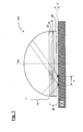
- Fig. 1 only schematically shows the structure of an optical element 100 in an imaging system according to the invention.
- the optical element 100 is preferably in particular the last image-side lens in a microlithographic projection objective whose fundamental structure is still described with reference to FIG Fig. 2 is explained.
- the optical element 100 is constructed from a first subelement 10 in the form of a plano-convex lens and a second subelement 20 in the form of a plane-parallel plate, wherein the light entry surface of the second subelement 20 is arranged directly adjacent to the light exit surface of the first subelement 10 and is preferably exploded thereon ,
- FIG. 1 The structure of the second partial element 20 from a total of four partial regions in the form of plane-parallel partial plates 21, 22, 23 and 24 is shown schematically.
- the second partial element 20 has a total of two partial regions, which have the same crystal section and are arranged rotated relative to one another around the element axis.
- the first sub-element 10 is made of a cubic crystalline material having such a refractive index, which is chosen in dependence on the numerical aperture NA of the imaging system so that the difference (n-NA) between this refractive index n and the numerical aperture NA of the imaging system maximum 0.2.
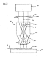
- a projection exposure apparatus 200 has an illumination device 201 and a projection objective 202.
- the projection objective 202 comprises a lens arrangement 203 with an aperture diaphragm AP, wherein an optical axis OA is defined by the lens arrangement 203, which is only schematically indicated.
- a mask 204 is arranged, which is held by means of a mask holder 205 in the beam path.
- Such masks 204 used in microlithography have a structure in the micrometer to nanometer range, which by means of the projection objective 202, for example reduced by a factor of 4 or 5 is reduced to an image plane IP.
- a photosensitive substrate 206, or a wafer, positioned by a substrate holder 207 is held.
- the still resolvable minimum structures depend on the wavelength ⁇ of the light used for the illumination as well as on the image-side numerical aperture of the projection lens 202, the maximum achievable resolution of the projection exposure apparatus 200 with decreasing wavelength ⁇ of the illumination device 201 and with increasing image-side numerical aperture of the projection lens 202 goes up.
- the projection lens 202 is configured as an imaging system according to the present invention.
- Fig. 2 is only schematically a possible, approximate position of an optical element 100 according to the invention indicated by dashed lines, wherein the optical element is arranged here according to a preferred embodiment, the image last optical element of the projection lens 202 and thus in the region of relatively high aperture angle.
- the optical element has the basis of Fig. 1 explained structure and is thus constructed in particular of a first sub-element 10 in the form of a plano-convex lens and a second sub-element 20 in the form of a plane-parallel plate according to the embodiments described above.
Abstract
Description
Die Erfindung betrifft ein Abbildungssystem, insbesondere ein Projektionsobjektiv einer mikrolithographischen Projektionsbelichtungsanlage. Insbesondere betrifft die Erfindung ein Projektionsobjektiv, welches den Einsatz hochbrechender Kristallmaterialien bei Begrenzung des negativen Einflusses der intrinsischen Doppelbrechung auf die Abbildungseigenschaften ermöglicht.The invention relates to an imaging system, in particular a projection objective of a microlithographic projection exposure apparatus. In particular, the invention relates to a projection lens which allows the use of high-index crystal materials while limiting the negative impact of intrinsic birefringence on the imaging properties.
In gegenwärtigen Mikrolithographie-Objektiven, insbesondere Immersionsobjektiven mit einem Wert der numerischen Apertur (NA) von mehr als 1.0, besteht in zunehmendem Maße ein Bedarf nach dem Einsatz von Materialien mit hohem Brechungsindex. Als "hoch" wird hier ein Brechungsindex bezeichnet, wenn sein Wert bei der gegebenen Wellenlänge den von Quarz, mit einem Wert von ca. 1,56 bei einer Wellenlänge von 193nm, übersteigt. Es sind eine Reihe von Materialien bekannt, deren Brechungsindex bei DUV- und VUV-Wellenlängen (<250nm) größer als 1,6 ist, beispielsweise Magnesiumspinell mit einem Brechungsindex von ca. 1.87 bei einer Wellenlänge von 193nm, oder Magnesiumoxid, dessen Brechungsindex bei 193nm etwa 2.0 beträgt.In current microlithography objectives, particularly immersion objectives having a numerical aperture (NA) value greater than 1.0, there is an increasing demand for the use of high refractive index materials. Here, a "refractive index" is referred to as "high" if its value at the given wavelength exceeds that of quartz, with a value of about 1.56 at a wavelength of 193 nm. There are a number of materials known whose refractive index at DUV and VUV wavelengths (<250nm) larger is about 1.6, for example, magnesium spinel having a refractive index of about 1.87 at a wavelength of 193 nm, or magnesium oxide whose refractive index at 193 nm is about 2.0.
Ein Problem beim Einsatz dieser Materialien als Linsenelemente besteht darin, dass sie durch ihre kubische Kristallstruktur intrinsische Doppelbrechung aufweisen, die mit niedriger Wellenlänge ansteigt, wobei z.B. Messungen der IDB-bedingten Verzögerung für Magnesiumspinell bei einer Wellenlänge von 193nm einen Wert von 52 nm/cm ergeben haben, und die IDBbedingte Verzögerung für Magnesiumoxid bei 193nm zu etwa 72 nm/cm abgeschätzt wurde. Eine solche Verzögerung kann je nach Designbedingungen im Bildfeld zu lateralen Strahlabweichungen führen, die das 3- bis 5-fache der abzubildenden Strukturbreite betragen.A problem with using these materials as lens elements is that they have intrinsic birefringence due to their cubic crystal structure, which increases with low wavelength, e.g. Measurements of the IDB-induced delay for magnesium spinel at a wavelength of 193 nm have given a value of 52 nm / cm, and the IDB-induced delay for magnesium oxide at 193 nm was estimated to be about 72 nm / cm. Depending on the design conditions, such a delay can lead to lateral beam deviations in the image field which are 3 to 5 times the pattern width to be imaged.
Zur Reduzierung des negativen Einflusses der intrinsischen Doppelbrechung in Fluoridkristall-Linsen auf die optische Abbildung ist es beispielsweise aus
Wenngleich durch dieses Verfahren eine gewisse Kompensation des negativen Einflusses der intrinsischen Doppelbrechung auch in den o.g. hochbrechenden kubischen Materialien erreichbar ist, besteht ein weiteres Problem darin, dass die Kompensation durch das o.g. "Clocking" dann unvollkommen ist, wenn die jeweiligen "Kompensationswege" (z.B. die jeweiligen Strahlwege der zur Interferenz gelangenden Strahlen in den zueinander verdrehten Bereichen des gleichen Kristallschnitts) unterschiedlich sind, wie es insbesondere bei außeraxialen Strahlbüscheln beispielsweise in einer bildseitig letzten plankonvexen Linse (als typischer Einsatzort des hochbrechenden Materials) der Fall ist. Dieser Umstand wirkt sich umso stärker aus, je stärker der Effekt der intrinsischen Doppelbrechung ist, was gerade einen Einsatz der o.g. hochbrechenden Materialien im bildnahen Bereich von Lithographie-Objektiven, z.B. als letztes Linsenelement, unter den dort auftretenden großen Strahlwinkeln, bei denen auch die intrinsische Doppelbrechung im (100)- und (111)- Kristallschnitt besonders hoch ist, erschwert.Although a certain compensation of the negative influence of the intrinsic birefringence can be achieved in the above high refractive index cubic materials by this method, another problem is that the compensation by the "clocking" mentioned above is imperfect when the respective "compensation paths" (eg the respective ones Beam paths of the rays reaching the interference in the mutually rotated regions of the same crystal section) are different, as is the case in particular in off-axis beam tufts, for example in a last image-plane plano-convex lens (as a typical site of use of high refractive index material). This circumstance affects the stronger, the stronger the effect of the intrinsic birefringence, which is just a use of the above-mentioned high-refractive materials in the near-field of lithographic lenses, eg as the last lens element, under the large beam angles occurring there, in which the intrinsic Birefringence in the (100) - and (111) - crystal section is particularly high, difficult.
Aus
Aufgabe der vorliegenden Erfindung ist es, ein Abbildungssystem, insbesondere ein Projektionsobjektiv einer mikrolithographischen Projektionsbelichtungsanlage bereitzustellen, welches den Einsatz hochbrechender Kristallmaterialien bei Begrenzung des negativen Einflusses intrinsischer Doppelbrechung ermöglicht.The object of the present invention is to provide an imaging system, in particular a projection objective of a microlithographic projection exposure apparatus, which enables the use of high-index crystal materials while limiting the negative influence of intrinsic birefringence.
Gemäß einem Aspekt der Erfindung umfasst ein erfindungsgemäßes Abbildungssystem, insbesondere ein Projektionsobjektiv einer mikrolithographischen Projektionsbelichtungsanlage, wenigstens ein optisches Element, welches ein kubisches Kristallmaterial aufweist, das bei einer vorgegebenen Arbeitswellenlänge eine Brechzahl n größer als 1.6 hat, und besitzt eine bildseitige numerische Apertur NA, welche kleiner als die Brechzahl n ist, wobei die Differenz (n-NA) zwischen der Brechzahl n und der numerischen Apertur NA des Abbildungssystems maximal 0.2 beträgt.According to one aspect of the invention, an imaging system according to the invention, in particular a projection objective of a microlithographic projection exposure apparatus, comprises at least one optical element which is a cubic crystal material which has a refractive index n greater than 1.6 at a given operating wavelength, and has an image-side numerical aperture NA which is smaller than the refractive index n, the difference (n-NA) between the refractive index n and the numerical aperture NA of the imaging system maximum is 0.2.
Die Erfindung geht dabei zunächst von der Erkenntnis aus, dass der Effekt der intrinsischen Doppelbrechung mit kürzer werdender Wellenlänge nicht linear ansteigt, sondern vielmehr zunächst allmählich einsetzt und dann mit fallender Wellenlänge dramatisch ansteigt. Diese Nichtlinearität ist umso stärker ausgeprägt, je mehr sich die jeweilige Arbeitswellenlänge der Absorptionskante (im UV-Bereich) für das betreffende Material nähert.The invention is initially based on the recognition that the effect of intrinsic birefringence does not increase linearly with shorter wavelength, but rather begins gradually and then increases dramatically with decreasing wavelength. This non-linearity is all the more pronounced as the respective working wavelength approaches the absorption edge (in the UV range) for the material in question.
Erfindungsgemäß wird nun das Potential an Materialien mit möglichst hohen Brechzahlen nicht ausgeschöpft, sondern die Brechzahl wird gerade so hoch (und nicht höher) gewählt, wie es erforderlich ist, um geometrisch Projektionslicht auch unter den maximal auftretenden Strahlwinkeln noch durch das Projektionsobjektiv zu koppeln und zur Abbildung zu bringen. Zugleich wird erfindungsgemäß die moderatere Anforderung an die Höhe der Brechzahl ausgenutzt, um ein solches Kristallmaterial auszuwählen, dessen Absorptionskante tiefer im UV liegt, so dass infolgedessen die intrinsische Doppelbrechung im Bereich der Arbeitswellenlänge noch kleiner bzw. weniger stark angestiegen ist, als dies bei einem Material mit höher liegender Absorptionskante der Fall ist.According to the invention, the potential of materials with the highest possible refractive indexes is not exhausted, but the refractive index is just as high (and not higher) chosen, as it is necessary to geometrically coupled projection light even at the maximum beam angles through the projection lens and Picture to bring. At the same time, according to the invention, the more moderate requirement for the height of the refractive index is exploited in order to select such a crystal material whose absorption edge lies deeper in the UV, as a result of which the intrinsic birefringence in the working wavelength has increased even smaller or less than in the case of a material with higher absorption edge is the case.
Bei einer numerischen Apertur von beispielsweise NA= 1.5 wird erfindungsgemäß, trotz gegebener Verfügbarkeit von bei typischen Arbeitswellenlängen von 193nm transparenten Materialien mit hohen Brechzahlen von beispielsweise n=1.87 (Magnesiumspinell) und darüber, bewusst auf die Wahl möglichst hochbrechender Kristallmaterialien verzichtet, sondern es wurden erfindungsgemäß vielmehr Materialien gesucht und gefunden, bei denen der Abstand der Brechzahl n zur (tieferliegenden) bildseitigen numerischen Apertur des Abbildungssystems geringer ist, aber gerade noch ausreicht, um das Projektionslicht auch unter maximal auftretenden Strahlwinkeln noch durch das Abbildungssystem zu koppeln bzw. zur Abbildung zu bringen.With a numerical aperture of, for example, NA = 1.5, according to the invention, despite the availability of transparent materials at typical operating wavelengths of 193 nm with high refractive indices of, for example, n = 1.87 (magnesium spinel) and above, deliberately dispensed with the choice of highly refractive crystal materials, but rather materials were sought and found according to the invention, in which the distance of the refractive index n to lower (lower) image-side numerical aperture of the imaging system lower is, but still just sufficient to couple the projection light even at maximum beam angles still through the imaging system or bring to imaging.
Gemäß einem weiteren Aspekt umfasst ein Abbildungssystem, insbesondere ein Projektionsobjektiv einer mikrolithographischen Projektionsbelichtungsanlage, wenigstens ein optisches Element, welches ein kubisches Kristallmaterial aufweist, das bei einer vorgegebenen Arbeitswellenlänge eine Brechzahl n hat, und besitzt eine bildseitige numerische Apertur NA, welche kleiner als die Brechzahl n ist, von wenigstens 1.50, wobei die Differenz (n-NA) zwischen der Brechzahl n und der numerischen Apertur NA des Abbildungssystems maximal 0.2 beträgt.According to a further aspect, an imaging system, in particular a projection objective of a microlithographic projection exposure apparatus, comprises at least one optical element which has a cubic crystal material which has a refractive index n at a predetermined operating wavelength and has a numerical aperture NA which is smaller than the refractive index n is, of at least 1.50, wherein the difference (n-NA) between the refractive index n and the numerical aperture NA of the imaging system is at most 0.2.
Vorzugsweise liegt die Differenz (n-NA) zwischen der Brechzahl n des optischen Elements und der numerischen Apertur NA des Abbildungssystems im Bereich von 0.05 bis 0.20, vorzugsweise im Bereich von 0.05 bis 0.15, und besonders bevorzugt im Bereich von 0.05 bis 0.10. Dabei wird durch die obere Grenze der Brechzahl wie oben ausgeführt eine Begrenzung der intrinsischen Doppelbrechung erreicht, während durch die untere Grenze der Brechzahl eine Begrenzung des Gesamtlinsenvolumens des Projektionsobjektivs erreicht wird.Preferably, the difference (n-NA) between the refractive index n of the optical element and the numerical aperture NA of the imaging system is in the range of 0.05 to 0.20, preferably in the range of 0.05 to 0.15, and more preferably in the range of 0.05 to 0.10. In this case, a limitation of the intrinsic birefringence is achieved by the upper limit of the refractive index as stated above, while limiting the total lens volume of the projection lens is achieved by the lower limit of the refractive index.
Weitere, durch die erfindungsgemäß zum Einsatz kommenden Materialien vorzugsweise zu erfüllende Kriterien sind eine hinreichende Stabilität gegenüber Luftfeuchtigkeit und UV-Licht, hohe Härte und gute optische Bearbeitbarkeit, sowie möglichst ungiftige Bestandteile.Further, by the materials used according to the invention preferably to be met criteria are sufficient Stability to humidity and UV light, high hardness and good optical workability, as well as non-toxic components.
In einer bevorzugen Ausführung weist das kubische Kristallmaterial ein Oxid auf, wofür eine ausreichende Transmission bei vergleichsweise hoher Brechzahl erhalten wurde.In a preferred embodiment, the cubic crystal material has an oxide, for which a sufficient transmission at a comparatively high refractive index was obtained.
In einer bevorzugen Ausführung weist das kubische Kristallmaterial Saphir (Al2O3) und ein Kalium- oder Kalziumoxid auf.In a preferred embodiment, the cubic crystal material comprises sapphire (Al 2 O 3 ) and a potassium or calcium oxide.
Insbesondere weist das kubische Kristallmaterial vorzugsweise wenigstens ein Material auf, welches aus der Gruppe ausgewählt ist, die 7Al2O3·12CaO, Al2O3·K2O, Al2O3·3CaO, Al2O3·SiO2KO, Al2O3-SiO2·2K und Al2O3·3CaO6H2O enthält.In particular 2, the cubic crystal material is preferably at least one material which is selected from the group 7Al 2 O 3 · 12CaO, Al 2 O 3 · K 2 O, Al 2 O 3 · 3CaO, Al 2 O 3 · SiO KO , Al 2 O 3 -SiO 2 · 2K and Al 2 O 3 · 3CaO6H 2 O.
Dabei bewirkt der Anteil von Saphir (Al2O3) eine Verbreiterung der Bandlücke bzw. eine Verschiebung der Absorptionskante in den UV-Bereich bei gleichzeitiger Erhöhung der Brechzahl, so dass brechzahlsenkende weitere Bestandteile den Mischkristall ergänzen, was zu der obigen Verringerung der intrinsischen Doppelbrechung führt.The proportion of sapphire (Al 2 O 3 ) causes a widening of the band gap or a shift of the absorption edge in the UV range while increasing the refractive index, so that additional refractive index components supplement the mixed crystal, resulting in the above reduction of intrinsic birefringence leads.
In einer weiteren bevorzugen Ausführung weist das kubische Kristallmaterial Kalzium, Natrium und Siliziumoxid auf. Insbesondere weist das kubische Kristallmaterial vorzugsweise wenigstens ein Material aus der Gruppe auf, die CaNa2SiO4 und CaNa4Si3O9 enthält.In another preferred embodiment, the cubic crystal material comprises calcium, sodium and silica. In particular, the cubic crystal material preferably comprises at least one material selected from the group consisting of CaNa 2 SiO 4 and CaNa 4 Si 3 O 9 .
In einer weiteren bevorzugen Ausführung weist das kubische Kristallmaterial wenigstens ein Material aus der Gruppe auf, die Sr(NO3)2, MgONa2O·SiO2 und Ca(NO3)2 enthält.In a further preferred embodiment, the cubic crystal material comprises at least one material from the group which Sr (NO 3) 2, MgONa 2 O · SiO 2 and Ca (NO 3) 2 contains.
Das optische Element ist vorzugsweise die bildseitig letzte brechende Linse des Abbildungssystems.The optical element is preferably the image-side last refractive lens of the imaging system.
Gemäß einer bevorzugten Ausführungsform ist das optische Element aus einem ersten Teilelement mit Brechkraft und einem zweiten, im Wesentlichen brechkraftlosen Teilelement zusammengesetzt. Vorzugsweise ist dabei das das erste Teilelement eine im Wesentlichen plankonvexe Linse, und das zweite Teilelement ist eine planparallele Platte.According to a preferred embodiment, the optical element is composed of a first partial element with refractive power and a second, substantially non-frictional partial element. In this case, the first subelement is preferably a substantially plano-convex lens, and the second subelement is a plane-parallel plate.
Ein solcher Aufbau des optischen Elements hat den Vorteil einer besonders effektiven Korrektur der sphärischen Aberration, welche typischerweise bei hohen Aperturen den größten zu bewältigenden Beitrag an Abbildungsfehlern darstellt. Bei telezentrischem Strahlengang im Bereich des optischen Elementes kann insbesondere durch das planparallele Teilelement in vorteilhafter Weise eine über das Bildfeld gleichmäßige Korrektur der sphärischen Aberration erreicht werden.Such a construction of the optical element has the advantage of a particularly effective correction of the spherical aberration, which is typically the largest contribution to aberrations to be handled at high apertures. In the case of a telecentric beam path in the region of the optical element, a correction of the spherical aberration which is uniform over the image field can advantageously be achieved, in particular by the plane-parallel subelement.
Im Gegensatz zu dem ersten Teilelement mit Brechkraft (d.h. insbesondere der plankonvexen Linse) treten in dem zweiten, in Wesentlichen brechkraftlosen Teilelement bei einem Aufbau aus gegeneinander verdrehten Teilbereichen des gleichen Kristallschnitts für die jeweiligen Teilbereiche jeweils im Wesentlichen gleiche Kompensationswege auf, so dass insoweit eine effektive Korrektur der intrinsischen Doppelbrechung im Wege des "Clocking-Schemas" erfolgen kann. Folglich ist es vorteilhaft, in dem zweiten, im Wesentlichen brechkraftlosen Teilelement ein zweites Material mit größerer Brechzahl als das Material in dem ersten Bereich vorzusehen, wobei diese größere Brechzahl insbesondere auch jenseits des o.g. Abstands von der numerischen Apertur liegen kann.In contrast to the first partial element with refractive power (ie, in particular the plano-convex lens) occur in the second, substantially no frictional partial element in a structure of mutually rotated portions of the same crystal section for the respective partial areas in each case substantially equal compensation paths, so far an effective Correction of the intrinsic birefringence can be done by way of the "clocking scheme". Consequently, it is advantageous to provide a second material having a greater refractive index than the material in the first region in the second, essentially non-frictional partial element, wherein this larger refractive index may in particular also lie beyond the above-mentioned distance from the numerical aperture.
In einer bevorzugten Ausführungsform ist daher das zweite Material aus der Gruppe Magnesiumspinell (MgAl2O4), Yttriumaluminiumgranat (Y3Al5O12), MgO und Scandiumaluminiumgranat (Sc3Al5O12) ausgewählt.In a preferred embodiment, therefore, the second material is selected from the group of magnesium spinel (MgAl 2 O 4 ), yttrium aluminum garnet (Y 3 Al 5 O 12 ), MgO and scandium aluminum garnet (Sc 3 Al 5 O 12 ).
Zur Kompensation der intrinsischen Doppelbrechung weist (zur Realisierung des Clocking-Schemas) das zweite Teilelement eine Elementachse und wenigstens zwei Teilbereiche auf, welche den gleichen Kristallschnitts aufweisen und gegeneinander um die Elementachse verdreht angeordnet sind.To compensate for the intrinsic birefringence, (for realizing the clocking scheme), the second subelement has an element axis and at least two subregions which have the same crystal section and are arranged rotated relative to one another around the element axis.
In einer Ausführung weisen der erste Teilbereich und der zweite Teilbereich jeweils einen (111)-Kristallschnitt auf und sind gegeneinander um 60°+k*120° (k=0, 1, 2,...) um die Elementachse verdreht angeordnet.In one embodiment, the first subregion and the second subregion each have a (111) crystal cut and are mutually rotated by 60 ° + k * 120 ° (k = 0, 1, 2, ...) about the element axis.
In einer weiteren Ausführung weisen der erste Teilbereich und der zweite Teilbereich jeweils einen (100)-Kristallschnitt auf und sind gegeneinander um 45°+1*90° (1=0,1,2,...) um die Elementachse verdreht angeordnet.In a further embodiment, the first subregion and the second subregion each have a (100) crystal cut and are arranged rotated by 45 ° + 1 * 90 ° (1 = 0,1,2,...) Around the element axis.
In einer weiteren Ausführung weist das zweite Teilelement eine Elementachse und wenigstens vier Teilbereiche auf, wobei ein erster Teilbereich und ein zweiter Teilbereich jeweils einen (111)-Kristallschnitt aufweisen und gegeneinander um 60°+k*120° (k=0,1,2,...) um die Elementachse verdreht angeordnet sind, und wobei ein dritter Teilbereich und ein vierter Teilbereich jeweils einen (100)-Kristallschnitt aufweisen und gegeneinander um 45°+1*90° (1=0,1,2,...) um die Elementachse verdreht angeordnet sind.In a further embodiment, the second subelement has an element axis and at least four subregions, wherein a first subregion and a second subregion each have a (111) crystal section and are mutually offset by 60 ° + k * 120 ° (k = 0,1,2 , ...) are arranged twisted about the element axis, and wherein a third partial area and a fourth partial area each have a (100) crystal section and are mutually inclined by 45 ° + 1 * 90 ° (1 = 0,1,2, .. .) Are arranged twisted about the element axis.
Die Erfindung betrifft ferner eine mikrolithographische Projektionsbelichtungsanlage sowie ein Verfahren zur Herstellung mikrolithographischer Bauelemente.The invention further relates to a microlithographic projection exposure apparatus and to a method for producing microlithographic components.
Weitere Ausgestaltungen der Erfindung sind der Beschreibung sowie den Unteransprüchen zu entnehmen.Further embodiments of the invention are described in the description and the dependent claims.
Die Erfindung wird nachstehend anhand von in den beigefügten Abbildungen dargestellten Ausführungsbeispielen näher erläutert.The invention will be explained in more detail with reference to embodiments shown in the accompanying drawings.
Es zeigen:
- Figur 1
- eine schematische Darstellung zur Erläuterung des Aufbaus eines optischen Elements in einem erfin- dungsgemäßen Abbildungssystem in einer bevorzugten Ausführungsform; und
- Figur 2
- eine schematische Darstellung des prinzipiellen Aufbaus einer Mikrolithographie- Projektionsbelichtungsanlage, welche ein erfin- dungsgemäßes Projektionsobjektiv aufweisen kann.
- FIG. 1
- a schematic representation for explaining the structure of an optical element in an inventive imaging system in a preferred embodiment; and
- FIG. 2
- a schematic representation of the basic structure of a microlithography projection exposure apparatus, which may have a projection objective according to the invention.
Gemäß
Ebenfalls in
In einer weiteren Ausführung weist das zweite Teilelement 20 insgesamt zwei Teilbereiche auf, welche den gleichen Kristallschnitt aufweisen und gegeneinander um die Elementachse verdreht angeordnet sind. Beispielsweise können diese Teilbereiche jeweils einen (100)-Kristallschnitt aufweisen und gegeneinander um 45°+1*90° (1=0,1,2,...) um die Elementachse verdreht angeordnet sein, oder die Teilbereiche können jeweils einen (111)-Kristallschnitt aufweisen und gegeneinander um 60°+k*120° (k=0, 1, 2,...) um die Elementachse ve.rdreht angeordnet sein.In a further embodiment, the second
Das erste Teilelement 10 ist aus einem kubisch kristallinen Material mit einer solchen Brechzahl hergestellt, die in Abhängigkeit von der numerischen Apertur NA des Abbildungssystems so gewählt ist, dass die Differenz (n-NA) zwischen dieser Brechzahl n und der numerischen Apertur NA des Abbildungssystems maximal 0.2 beträgt.The
Legt man eine beispielhafte numerische Apertur des Projektionsobjektivs von NA=1.5 zugrunde, so beträgt somit die Brechzahl n des kubisch kristallinen Materials des ersten Teilelements maximal n=1.7.If one assumes an exemplary numerical aperture of the projection objective of NA = 1.5, then the refractive index n of the cubic crystalline material of the first subelement is at most n = 1.7.
Eine Auflistung über erfindungsgemäß besonders geeignete Materialien gibt die nachfolgende Tabelle 1. Dabei ist in Spalte 2 jeweils die zu dem Kristallmaterial gehörige Brechzahl nd bei der Wellenlänge λ=589nm angegeben; hierbei ist darauf hinzuweisen, dass die Brechzahl bei einer gebräuchlichen Arbeitswellenlänge von λ=193nm typischerweise um etwa 0.1 größer ist.
Gemäß
Das Projektionsobjektiv 202 ist als Abbildungssystem gemäß der vorliegenden Erfindung ausgestaltet. In
Wenn die Erfindung auch anhand spezieller Ausführungsformen beschrieben wurde, erschließen sich für den Fachmann zahlreiche Variationen und alternative Ausführungsformen, z.B. durch Kombination und/oder Austausch von Merkmalen einzelner Ausführungsformen. Dementsprechend versteht es sich für den Fachmann, dass derartige Variationen und alternative Ausführungsformen von der vorliegenden Erfindung mit umfasst sind, und die Reichweite der Erfindung nur im Sinne der beigefügten Patentansprüche und deren Äquivalente beschränkt ist.Although the invention has also been described with reference to specific embodiments, numerous variations and alternative embodiments will be apparent to those skilled in the art, eg, by combining and / or replacing features of individual embodiments. Accordingly, it will be understood by those skilled in the art that such variations and alternative embodiments are encompassed by the present invention. and the scope of the invention is limited only in terms of the appended claims and their equivalents.
Claims (23)
- Imaging system, in particular a projection lens of a microlithographic projection exposure apparatus, with• at least one optical element (100) which comprises a cubic-crystalline material having a refractive index n that is larger than 1.6 at a given operating wavelength;• and an image-side numerical aperture NA that is smaller than the refractive index n;• wherein the difference (n-NA) between the refractive index n and the numerical aperture NA of the imaging system is at most 0.2.
- Imaging system, in particular a projection lens of a microlithographic projection exposure apparatus, with• at least one optical element (100) which comprises a cubic-crystalline material having a refractive index n at a given operating wavelength;• and an image-side numerical aperture NA, that is smaller than the refractive index n, of at least 1.50;• wherein the difference (n-NA) between the refractive index n and the numerical aperture NA of the imaging system is at most 0.2.
- Imaging system according to claim 1 or 2, characterized in that the difference (n-NA) between the refractive index n and the numerical aperture NA lies in the range from 0.05 to 0.20.
- Imaging system according to one of the preceding claims, characterized in that the cubic-crystalline material comprises an oxide.
- Imaging system according to claim 4, characterized in that the cubic-crystalline material comprises sapphire (Al2O3) and a potassium- or calcium oxide.
- Imaging system according to one of the preceding claims, characterized in that the cubic-crystalline material comprises at least one material selected from the group that contains 7Al2O3·12CaO, Al2O3·K2O, Al2O3·3CaO, Al2O3·SiO2KO, Al2O3·SiO2·2K and Al2O3·3CaO6H2O.
- Imaging system according to one of the preceding claims, characterized in that the cubic-crystalline material comprises calcium, sodium and silicon oxide.
- Imaging system according to one of the preceding claims, characterized in that the cubic-crystalline material comprises at least one material selected from the group that contains CaNa2SiO4, CaNa4Si3O9, Sr(NO3)2, MgONa2O·SiO2 und Ca (NO3)2.
- Imaging system according to one of the preceding claims, characterized in that the optical element (100) is a lens with refractive power located in last position to the image side of the imaging system.
- Imaging system according to one of the preceding claims, characterized in that the optical element (100) has a planar light-exit surface.
- Imaging system according to one of the preceding claims, characterized in that the optical element (100) has a light-entrance surface that is convex-curved at the object-side.
- Imaging system according to one of the preceding claims, characterized in that the optical element (100) is composed of a first partial element (10) having refractive power and a second partial element (20) having substantially no refractive power.
- Imaging system according to claim 12, characterized in that the first partial element (10) is a substantially planar-convex lens.
- Imaging system according to claim 12 or 13, characterized in that the second partial element (20) is a planar-parallel plate.
- Imaging system according to one of the claims 12 to 14, characterized in that the cubic-crystalline material is present in the first partial element (10), while the second partial element (20) which is substantially without refractive power comprises a second material with a larger refractive index than the material in the first partial element (10).
- Imaging system according to claim 15, characterized in that the second material is selected from the group that contains magnesium spinel (MgAl2O4), yttrium aluminum garnet (Y3Al5O12), magnesium oxide (MgO) und scandium aluminum garnet (Sc3Al5O12).
- Imaging system according to one of the claims 12 to 16, characterized in that the second partial element (20) has an element axis and at least two portions (21, 22) that are of the same crystallographic cut and are arranged rotated relative to each other about the element axis.
- Imaging system according to claim 17, characterized in that the first portion (21) and the second portion (22) are each of a crystallographic (111)-cut and are arranged rotated relative to each other by 60°+ k*120° (k = 0, 1, 2, ...) about the element axis.
- Imaging system according to claim 17, characterized in that the first portion and the second portion are each of a crystallographic (100)-cut and are arranged rotated relative to each other by 45°+ 1*90° (1 = 0, 1, 2, ...) about the element axis.
- Imaging system according to one of the claims 12 to 19, characterized in that the second partial element has an element axis and at least four portions (21-24), wherein a first portion (21) and a second portion (22) are each of a crystallographic (111)-cut and are arranged with their orientations rotated relative to each other by 60°+ k*120o (k = 0, 1, 2, ...) about the element axis, and wherein a third portion (23) and a fourth portion (24) are each of a crystallographic (100)-cut and are arranged rotated relative to each other by 45°+ 1*90° (1 = 0, 1, 2, ...) about the element axis.
- Imaging system according to one of the preceding claims, characterized in that the operating wavelength is shorter than 250 nm, preferably shorter than 200 nm.
- Microlithographic projection exposure apparatus with a projection lens that is an imaging system according to one of the preceding claims.
- Method for the microlithographic manufacture of micro-structured components, with the following steps:• providing a substrate (206) on at least part of which a coating of a light-sensitive material is deposited;• providing a mask (204) which carries structures of which an image is to be formed;• providing a projection exposure apparatus (200) according to claim 22;• projecting at least a part of the mask (204) onto an area of the coating by means of the projection exposure apparatus (200).
Applications Claiming Priority (2)
| Application Number | Priority Date | Filing Date | Title |
|---|---|---|---|
| US70690305P | 2005-08-10 | 2005-08-10 | |
| PCT/EP2006/065070 WO2007017473A1 (en) | 2005-08-10 | 2006-08-04 | Imaging system, in particular projection lens of a microlithographic projection exposure unit |
Publications (2)
| Publication Number | Publication Date |
|---|---|
| EP1913445A1 EP1913445A1 (en) | 2008-04-23 |
| EP1913445B1 true EP1913445B1 (en) | 2011-05-25 |
Family
ID=37188852
Family Applications (1)
| Application Number | Title | Priority Date | Filing Date |
|---|---|---|---|
| EP06778169A Not-in-force EP1913445B1 (en) | 2005-08-10 | 2006-08-04 | Imaging system, in particular projection lens of a microlithographic projection exposure unit |
Country Status (7)
| Country | Link |
|---|---|
| US (1) | US20080182210A1 (en) |
| EP (1) | EP1913445B1 (en) |
| JP (1) | JP2009505124A (en) |
| KR (1) | KR20080028429A (en) |
| CN (1) | CN101243359B (en) |
| AT (1) | ATE511124T1 (en) |
| WO (1) | WO2007017473A1 (en) |
Families Citing this family (2)
| Publication number | Priority date | Publication date | Assignee | Title |
|---|---|---|---|---|
| DE102008001800A1 (en) * | 2007-05-25 | 2008-11-27 | Carl Zeiss Smt Ag | Projection lens for microlithography, microlithography projection exposure apparatus with such a projection lens, microlithographic manufacturing method for components as well as produced by this method component |
| CN114326075B (en) * | 2021-12-10 | 2023-12-19 | 肯维捷斯(武汉)科技有限公司 | Digital microscopic imaging system and microscopic detection method for biological sample |
Family Cites Families (12)
| Publication number | Priority date | Publication date | Assignee | Title |
|---|---|---|---|---|
| KR20000034967A (en) * | 1998-11-30 | 2000-06-26 | 헨켈 카르스텐 | Objective with crystal-lenses and projection-illuminating-device |
| US6995930B2 (en) * | 1999-12-29 | 2006-02-07 | Carl Zeiss Smt Ag | Catadioptric projection objective with geometric beam splitting |
| KR20040015251A (en) * | 2001-05-15 | 2004-02-18 | 칼 짜이스 에스엠티 아게 | Objective with fluoride crystal lenses |
| JP2003021619A (en) * | 2001-07-05 | 2003-01-24 | Canon Inc | Fluorite and its analyzing method, manufacturing method and optical, characteristic evaluation method |
| JPWO2003009015A1 (en) * | 2001-07-18 | 2004-11-11 | 株式会社ニコン | Optical element with lanthanum fluoride film |
| US7092069B2 (en) * | 2002-03-08 | 2006-08-15 | Carl Zeiss Smt Ag | Projection exposure method and projection exposure system |
| EP1535100A1 (en) * | 2002-09-03 | 2005-06-01 | Carl Zeiss SMT AG | Objective with birefringent lenses |
| WO2005006417A1 (en) * | 2003-07-09 | 2005-01-20 | Nikon Corporation | Exposure apparatus and method for manufacturing device |
| US7466489B2 (en) * | 2003-12-15 | 2008-12-16 | Susanne Beder | Projection objective having a high aperture and a planar end surface |
| WO2005059617A2 (en) * | 2003-12-15 | 2005-06-30 | Carl Zeiss Smt Ag | Projection objective having a high aperture and a planar end surface |
| WO2005059645A2 (en) * | 2003-12-19 | 2005-06-30 | Carl Zeiss Smt Ag | Microlithography projection objective with crystal elements |
| JP2006113533A (en) * | 2004-08-03 | 2006-04-27 | Nikon Corp | Projection optical system, exposure apparatus, and exposure method |
-
2006
- 2006-08-04 AT AT06778169T patent/ATE511124T1/en active
- 2006-08-04 JP JP2008525556A patent/JP2009505124A/en active Pending
- 2006-08-04 WO PCT/EP2006/065070 patent/WO2007017473A1/en active Application Filing
- 2006-08-04 CN CN2006800296095A patent/CN101243359B/en not_active Expired - Fee Related
- 2006-08-04 EP EP06778169A patent/EP1913445B1/en not_active Not-in-force
- 2006-08-04 KR KR1020087001045A patent/KR20080028429A/en active Search and Examination
-
2008
- 2008-02-07 US US12/027,731 patent/US20080182210A1/en not_active Abandoned
Also Published As
| Publication number | Publication date |
|---|---|
| ATE511124T1 (en) | 2011-06-15 |
| US20080182210A1 (en) | 2008-07-31 |
| CN101243359B (en) | 2011-04-06 |
| JP2009505124A (en) | 2009-02-05 |
| WO2007017473A1 (en) | 2007-02-15 |
| CN101243359A (en) | 2008-08-13 |
| EP1913445A1 (en) | 2008-04-23 |
| KR20080028429A (en) | 2008-03-31 |
Similar Documents
| Publication | Publication Date | Title |
|---|---|---|
| EP1122608B1 (en) | Projection exposure system with reflective reticle | |
| DE60026623T2 (en) | Catadioptric optical system and exposure device with such a system | |
| EP1260845A2 (en) | Catadioptric reduction lens | |
| DE19902336A1 (en) | Optical projection system for manufacturing semiconductor components | |
| DE10133841A1 (en) | Lens with crystal lenses | |
| EP1282011A2 (en) | Reflective projection lens for EUV photolithography | |
| EP1097404A1 (en) | Projection lens for microlithography | |
| DE3439297C2 (en) | Mirror lens lens | |
| DE102008007449A1 (en) | Illumination optics for illuminating an object field of a projection exposure apparatus for microlithography | |
| DE102010001388A1 (en) | Facet mirror for use in microlithography | |
| DE19833481A1 (en) | Projection optical system for exposure system used in semiconductor device, liquid crystal display element manufacture | |
| DE102008040613A1 (en) | Optical system of a microlithographic projection exposure apparatus | |
| DE102013008814A1 (en) | Large format catadioptric unit magnification optics for microlithography | |
| EP1102100A2 (en) | Catadioptric objective with beamsplitter | |
| DE102006013560A1 (en) | Projection lens for micro lithographic projection illumination system, has lens , to characterizes symmetry axis of another lens by rotation of orientation of crystal axes, where lenses are separated by gap filled with liquid | |
| WO2006125790A2 (en) | Imaging systems in particular for a microlithographic projection illumination unit | |
| DE102016205619A1 (en) | Attenuation filter for projection objective, projection objective with attenuation filter for projection exposure apparatus and projection exposure apparatus with projection objective | |
| EP1913445B1 (en) | Imaging system, in particular projection lens of a microlithographic projection exposure unit | |
| DE102006025044A1 (en) | Projection lens for microlithographic projection exposure system, has two optical units that are so designed that they are not rotationally symmetric to optical axis, where each unit generates one respective distribution of time delay | |
| DE602004006051T2 (en) | Optical projection system | |
| DE102022205700A1 (en) | Projection lens, projection exposure system and projection exposure method | |
| DE102006028242A1 (en) | Projection objective of micro-lithographic projection exposure equipment e.g. for fabrication of integrated circuits, has diffractive optical element arranged in pupil plane | |
| EP1471539A1 (en) | Imaging system for microscope based on extreme ultraviolet (EUV) radiation | |
| DE10224361A1 (en) | Very large aperture projection objective has essentially symmetrical arrangement of bi-convex lenses and negative meniscus lenses near system aperture at distance before image plane | |
| DE102017207582A1 (en) | Projection objective, projection exposure apparatus and projection exposure method |
Legal Events
| Date | Code | Title | Description |
|---|---|---|---|
| PUAI | Public reference made under article 153(3) epc to a published international application that has entered the european phase |
Free format text: ORIGINAL CODE: 0009012 |
|
| 17P | Request for examination filed |
Effective date: 20080205 |
|
| AK | Designated contracting states |
Kind code of ref document: A1 Designated state(s): AT BE BG CH CY CZ DE DK EE ES FI FR GB GR HU IE IS IT LI LT LU LV MC NL PL PT RO SE SI SK TR |
|
| 17Q | First examination report despatched |
Effective date: 20100823 |
|
| GRAP | Despatch of communication of intention to grant a patent |
Free format text: ORIGINAL CODE: EPIDOSNIGR1 |
|
| DAX | Request for extension of the european patent (deleted) | ||
| RAP1 | Party data changed (applicant data changed or rights of an application transferred) |
Owner name: CARL ZEISS SMT GMBH |
|
| GRAS | Grant fee paid |
Free format text: ORIGINAL CODE: EPIDOSNIGR3 |
|
| GRAA | (expected) grant |
Free format text: ORIGINAL CODE: 0009210 |
|
| AK | Designated contracting states |
Kind code of ref document: B1 Designated state(s): AT BE BG CH CY CZ DE DK EE ES FI FR GB GR HU IE IS IT LI LT LU LV MC NL PL PT RO SE SI SK TR |
|
| REG | Reference to a national code |
Ref country code: GB Ref legal event code: FG4D Free format text: NOT ENGLISH |
|
| REG | Reference to a national code |
Ref country code: CH Ref legal event code: EP |
|
| REG | Reference to a national code |
Ref country code: IE Ref legal event code: FG4D Free format text: LANGUAGE OF EP DOCUMENT: GERMAN |
|
| REG | Reference to a national code |
Ref country code: DE Ref legal event code: R096 Ref document number: 502006009577 Country of ref document: DE Effective date: 20110707 |
|
| REG | Reference to a national code |
Ref country code: NL Ref legal event code: VDEP Effective date: 20110525 |
|
| PG25 | Lapsed in a contracting state [announced via postgrant information from national office to epo] |
Ref country code: SE Free format text: LAPSE BECAUSE OF FAILURE TO SUBMIT A TRANSLATION OF THE DESCRIPTION OR TO PAY THE FEE WITHIN THE PRESCRIBED TIME-LIMIT Effective date: 20110525 Ref country code: LT Free format text: LAPSE BECAUSE OF FAILURE TO SUBMIT A TRANSLATION OF THE DESCRIPTION OR TO PAY THE FEE WITHIN THE PRESCRIBED TIME-LIMIT Effective date: 20110525 Ref country code: PT Free format text: LAPSE BECAUSE OF FAILURE TO SUBMIT A TRANSLATION OF THE DESCRIPTION OR TO PAY THE FEE WITHIN THE PRESCRIBED TIME-LIMIT Effective date: 20110926 |
|
| PG25 | Lapsed in a contracting state [announced via postgrant information from national office to epo] |
Ref country code: GR Free format text: LAPSE BECAUSE OF FAILURE TO SUBMIT A TRANSLATION OF THE DESCRIPTION OR TO PAY THE FEE WITHIN THE PRESCRIBED TIME-LIMIT Effective date: 20110826 Ref country code: ES Free format text: LAPSE BECAUSE OF FAILURE TO SUBMIT A TRANSLATION OF THE DESCRIPTION OR TO PAY THE FEE WITHIN THE PRESCRIBED TIME-LIMIT Effective date: 20110905 Ref country code: IS Free format text: LAPSE BECAUSE OF FAILURE TO SUBMIT A TRANSLATION OF THE DESCRIPTION OR TO PAY THE FEE WITHIN THE PRESCRIBED TIME-LIMIT Effective date: 20110925 Ref country code: FI Free format text: LAPSE BECAUSE OF FAILURE TO SUBMIT A TRANSLATION OF THE DESCRIPTION OR TO PAY THE FEE WITHIN THE PRESCRIBED TIME-LIMIT Effective date: 20110525 Ref country code: SI Free format text: LAPSE BECAUSE OF FAILURE TO SUBMIT A TRANSLATION OF THE DESCRIPTION OR TO PAY THE FEE WITHIN THE PRESCRIBED TIME-LIMIT Effective date: 20110525 Ref country code: LV Free format text: LAPSE BECAUSE OF FAILURE TO SUBMIT A TRANSLATION OF THE DESCRIPTION OR TO PAY THE FEE WITHIN THE PRESCRIBED TIME-LIMIT Effective date: 20110525 Ref country code: CY Free format text: LAPSE BECAUSE OF FAILURE TO SUBMIT A TRANSLATION OF THE DESCRIPTION OR TO PAY THE FEE WITHIN THE PRESCRIBED TIME-LIMIT Effective date: 20110525 |
|
| REG | Reference to a national code |
Ref country code: IE Ref legal event code: FD4D |
|
| PG25 | Lapsed in a contracting state [announced via postgrant information from national office to epo] |
Ref country code: NL Free format text: LAPSE BECAUSE OF FAILURE TO SUBMIT A TRANSLATION OF THE DESCRIPTION OR TO PAY THE FEE WITHIN THE PRESCRIBED TIME-LIMIT Effective date: 20110525 |
|
| PG25 | Lapsed in a contracting state [announced via postgrant information from national office to epo] |
Ref country code: CZ Free format text: LAPSE BECAUSE OF FAILURE TO SUBMIT A TRANSLATION OF THE DESCRIPTION OR TO PAY THE FEE WITHIN THE PRESCRIBED TIME-LIMIT Effective date: 20110525 Ref country code: EE Free format text: LAPSE BECAUSE OF FAILURE TO SUBMIT A TRANSLATION OF THE DESCRIPTION OR TO PAY THE FEE WITHIN THE PRESCRIBED TIME-LIMIT Effective date: 20110525 Ref country code: IE Free format text: LAPSE BECAUSE OF FAILURE TO SUBMIT A TRANSLATION OF THE DESCRIPTION OR TO PAY THE FEE WITHIN THE PRESCRIBED TIME-LIMIT Effective date: 20110525 |
|
| BERE | Be: lapsed |
Owner name: CARL ZEISS SMT G.M.B.H. Effective date: 20110831 |
|
| PG25 | Lapsed in a contracting state [announced via postgrant information from national office to epo] |
Ref country code: RO Free format text: LAPSE BECAUSE OF FAILURE TO SUBMIT A TRANSLATION OF THE DESCRIPTION OR TO PAY THE FEE WITHIN THE PRESCRIBED TIME-LIMIT Effective date: 20110525 Ref country code: DK Free format text: LAPSE BECAUSE OF FAILURE TO SUBMIT A TRANSLATION OF THE DESCRIPTION OR TO PAY THE FEE WITHIN THE PRESCRIBED TIME-LIMIT Effective date: 20110525 Ref country code: SK Free format text: LAPSE BECAUSE OF FAILURE TO SUBMIT A TRANSLATION OF THE DESCRIPTION OR TO PAY THE FEE WITHIN THE PRESCRIBED TIME-LIMIT Effective date: 20110525 Ref country code: PL Free format text: LAPSE BECAUSE OF FAILURE TO SUBMIT A TRANSLATION OF THE DESCRIPTION OR TO PAY THE FEE WITHIN THE PRESCRIBED TIME-LIMIT Effective date: 20110525 |
|
| PG25 | Lapsed in a contracting state [announced via postgrant information from national office to epo] |
Ref country code: MC Free format text: LAPSE BECAUSE OF NON-PAYMENT OF DUE FEES Effective date: 20110831 |
|
| PLBE | No opposition filed within time limit |
Free format text: ORIGINAL CODE: 0009261 |
|
| REG | Reference to a national code |
Ref country code: CH Ref legal event code: PL |
|
| STAA | Information on the status of an ep patent application or granted ep patent |
Free format text: STATUS: NO OPPOSITION FILED WITHIN TIME LIMIT |
|
| GBPC | Gb: european patent ceased through non-payment of renewal fee |
Effective date: 20110825 |
|
| PG25 | Lapsed in a contracting state [announced via postgrant information from national office to epo] |
Ref country code: CH Free format text: LAPSE BECAUSE OF NON-PAYMENT OF DUE FEES Effective date: 20110831 Ref country code: LI Free format text: LAPSE BECAUSE OF NON-PAYMENT OF DUE FEES Effective date: 20110831 |
|
| 26N | No opposition filed |
Effective date: 20120228 |
|
| PG25 | Lapsed in a contracting state [announced via postgrant information from national office to epo] |
Ref country code: BE Free format text: LAPSE BECAUSE OF NON-PAYMENT OF DUE FEES Effective date: 20110831 Ref country code: IT Free format text: LAPSE BECAUSE OF FAILURE TO SUBMIT A TRANSLATION OF THE DESCRIPTION OR TO PAY THE FEE WITHIN THE PRESCRIBED TIME-LIMIT Effective date: 20110525 |
|
| REG | Reference to a national code |
Ref country code: DE Ref legal event code: R119 Ref document number: 502006009577 Country of ref document: DE Effective date: 20120301 |
|
| REG | Reference to a national code |
Ref country code: DE Ref legal event code: R097 Ref document number: 502006009577 Country of ref document: DE Effective date: 20120228 |
|
| PG25 | Lapsed in a contracting state [announced via postgrant information from national office to epo] |
Ref country code: GB Free format text: LAPSE BECAUSE OF NON-PAYMENT OF DUE FEES Effective date: 20110825 |
|
| REG | Reference to a national code |
Ref country code: AT Ref legal event code: MM01 Ref document number: 511124 Country of ref document: AT Kind code of ref document: T Effective date: 20110804 |
|
| PG25 | Lapsed in a contracting state [announced via postgrant information from national office to epo] |
Ref country code: AT Free format text: LAPSE BECAUSE OF NON-PAYMENT OF DUE FEES Effective date: 20110804 |
|
| PG25 | Lapsed in a contracting state [announced via postgrant information from national office to epo] |
Ref country code: LU Free format text: LAPSE BECAUSE OF NON-PAYMENT OF DUE FEES Effective date: 20110804 |
|
| PG25 | Lapsed in a contracting state [announced via postgrant information from national office to epo] |
Ref country code: BG Free format text: LAPSE BECAUSE OF FAILURE TO SUBMIT A TRANSLATION OF THE DESCRIPTION OR TO PAY THE FEE WITHIN THE PRESCRIBED TIME-LIMIT Effective date: 20110825 Ref country code: DE Free format text: LAPSE BECAUSE OF NON-PAYMENT OF DUE FEES Effective date: 20120301 |
|
| PG25 | Lapsed in a contracting state [announced via postgrant information from national office to epo] |
Ref country code: TR Free format text: LAPSE BECAUSE OF FAILURE TO SUBMIT A TRANSLATION OF THE DESCRIPTION OR TO PAY THE FEE WITHIN THE PRESCRIBED TIME-LIMIT Effective date: 20110525 |
|
| PG25 | Lapsed in a contracting state [announced via postgrant information from national office to epo] |
Ref country code: HU Free format text: LAPSE BECAUSE OF FAILURE TO SUBMIT A TRANSLATION OF THE DESCRIPTION OR TO PAY THE FEE WITHIN THE PRESCRIBED TIME-LIMIT Effective date: 20110525 |
|
| REG | Reference to a national code |
Ref country code: FR Ref legal event code: PLFP Year of fee payment: 11 |
|
| REG | Reference to a national code |
Ref country code: FR Ref legal event code: PLFP Year of fee payment: 12 |
|
| PGFP | Annual fee paid to national office [announced via postgrant information from national office to epo] |
Ref country code: FR Payment date: 20170822 Year of fee payment: 12 |
|
| PG25 | Lapsed in a contracting state [announced via postgrant information from national office to epo] |
Ref country code: FR Free format text: LAPSE BECAUSE OF NON-PAYMENT OF DUE FEES Effective date: 20180831 |