EP1903804A2 - Lesesignalprozessor, Bildlesevorrichtung und Bilderzeugungsvorrichtung - Google Patents
Lesesignalprozessor, Bildlesevorrichtung und Bilderzeugungsvorrichtung Download PDFInfo
- Publication number
- EP1903804A2 EP1903804A2 EP07253517A EP07253517A EP1903804A2 EP 1903804 A2 EP1903804 A2 EP 1903804A2 EP 07253517 A EP07253517 A EP 07253517A EP 07253517 A EP07253517 A EP 07253517A EP 1903804 A2 EP1903804 A2 EP 1903804A2
- Authority
- EP
- European Patent Office
- Prior art keywords
- colors
- signal processor
- output
- signals
- digital data
- Prior art date
- Legal status (The legal status is an assumption and is not a legal conclusion. Google has not performed a legal analysis and makes no representation as to the accuracy of the status listed.)
- Granted
Links
- 239000003086 colorant Substances 0.000 claims abstract description 30
- 238000012545 processing Methods 0.000 description 39
- 238000010586 diagram Methods 0.000 description 20
- 230000005540 biological transmission Effects 0.000 description 15
- 230000003287 optical effect Effects 0.000 description 7
- 238000012546 transfer Methods 0.000 description 7
- 230000000694 effects Effects 0.000 description 6
- 238000000926 separation method Methods 0.000 description 6
- 238000006243 chemical reaction Methods 0.000 description 4
- 238000005516 engineering process Methods 0.000 description 4
- 230000003321 amplification Effects 0.000 description 3
- 238000003199 nucleic acid amplification method Methods 0.000 description 3
- 238000005070 sampling Methods 0.000 description 3
- 101100113692 Caenorhabditis elegans clk-2 gene Proteins 0.000 description 2
- 108010076504 Protein Sorting Signals Proteins 0.000 description 2
- 230000008878 coupling Effects 0.000 description 2
- 238000010168 coupling process Methods 0.000 description 2
- 238000005859 coupling reaction Methods 0.000 description 2
- 229910052736 halogen Inorganic materials 0.000 description 2
- 150000002367 halogens Chemical class 0.000 description 2
- 230000009467 reduction Effects 0.000 description 2
- 239000007787 solid Substances 0.000 description 2
- 239000003990 capacitor Substances 0.000 description 1
- 238000010276 construction Methods 0.000 description 1
- 238000012937 correction Methods 0.000 description 1
- 239000011521 glass Substances 0.000 description 1
- 238000000034 method Methods 0.000 description 1
- 238000012986 modification Methods 0.000 description 1
- 230000004048 modification Effects 0.000 description 1
- 230000008569 process Effects 0.000 description 1
- 230000004044 response Effects 0.000 description 1
- 230000008054 signal transmission Effects 0.000 description 1
- 230000011664 signaling Effects 0.000 description 1
- 230000003068 static effect Effects 0.000 description 1
Images








Classifications
-
- H—ELECTRICITY
- H04—ELECTRIC COMMUNICATION TECHNIQUE
- H04N—PICTORIAL COMMUNICATION, e.g. TELEVISION
- H04N23/00—Cameras or camera modules comprising electronic image sensors; Control thereof
- H04N23/80—Camera processing pipelines; Components thereof
- H04N23/84—Camera processing pipelines; Components thereof for processing colour signals
Definitions
- the present invention relates to a read signal processor, an image reading apparatus, and an image forming apparatus.
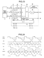
- Fig. 23 is a schematic block diagram of a typical signal processor in a typical image reading apparatus.
- an analog signal processing IC 10 having three inputs, RIN for red (R), GIN for green (G), and BIN for blue (B), is used corresponding to a color linear image sensor 1 having three outputs: RO for red, GO for green, and BO for blue.
- the analog signal processing IC 10 includes, with respect to each of the inputs, a clamp circuit (CLMP) 11 for setting an input terminal potential after alternate-current coupling, a sample-hold (SH) circuit 12 for extracting signal components of only the output signal of the color linear image sensor 1, and a variable gain amplifier (VGA) 13 for amplifying sample-hold signals based on a designated amplification rate.
- CLMP clamp circuit
- SH sample-hold circuit
- VGA variable gain amplifier
- the analog signal processing IC 10 includes a timing generator & interface (TG&IF) 16 that receives from outside a CLMPIN signal, an SH signal, and an MCLK signal.
- the CLMPIN signal is a gate signal for controlling the clamp circuits 11.
- the SH signal is a sample clock for sampling a signal area of image signals in the SH circuits 12.
- the MCLK signal is a reference clock for controlling the AMPX 14 and the ADC 15.
- An RMB signal is an identification signal for indicating timing of RED data.
- the variable gain amplifier 13 includes a register for holding a gain set value received through a data/address bus.
- Fig. 24 is timing chart for explaining output timings of the signals RIN, GIN, BIN, SH, MCLK, M1, M2, DO[9:0], and RMB.
- Japanese Patent Applications Laid-open Nos. 2002-199213 (patent document 1) and 2002-281325 (patent document 2) disclose related technology.
- the technology disclosed in the patent document 1 provides an image reading apparatus capable of alleviating an output difference between an odd pixel and an even pixel.
- the image reading apparatus disclosed in the patent document 1 includes an optical unit (a halogen lamp and a lens unit) for reading an image on a document, a solid image sensor (CCD) for performing photoelectric conversion to optical data and outputting image data that corresponds to the document image when the optical data read by the optical unit is input, an analog signal processor (a sample-hold circuit, a black-level correction circuit, an amplification circuit) that processes image signals output from the solid image sensor in an analog way, and two of A/D converters that are arranged for each channel of RGB and A/D convert image signals processed by the analog signal processor.
- the two of A/D converters include two types of input clocks that are different in phase.
- the technology disclosed in the patent document 2 provides a color image reading apparatus that can exchange R/B image data with a simple configuration and performs signal processing with respect to image data read from a RGB 3 line linear sensor.
- the image reading apparatus disclosed in the patent document 2 includes the internal function of exchanging R/B image data with an ASIC for performing signal processing to a CCD, motor, and lamp driving signal and image data and R/G image data is exchanged through the function.
- the conventional signal processing IC is effective for a color linear image sensor with a relatively low pixel rate (up to about 10 megahertz per color), that is, when the output from a color linear image sensor is through one channel per one color.
- pixel rate up to about 10 megahertz per color
- image data is to be transmitted for a longer distance (a few tens of centimeters or more)
- the conventional signal processing IC is disadvantageous in terms of mounting area and component costs.
- a read signal processor including a sample-hold unit that sample-holds a designated range of each pixel of a sensor output signal for each color with respect to output from a color linear image sensor corresponding to three colors, and outputs a sample-held signal corresponding to each of the colors; an amplifying unit that amplifies the sample-held signals based on a set gain, and outputs an amplified signal corresponding to each of the colors; a converting unit that analog-digital converts the amplified signals to obtain digital data for each of the colors; and an output unit that serializes a plurality of bits of the digital data for each of the colors to obtain a plurality of serial signals, converts the serial signals to a plurality of low-amplitude differential signals, and outputs the serial low-amplitude differential signals.
- a read signal processor including a sample-hold unit that sample-holds a designated range of each pixel of a sensor output signal for each color with respect to output from a color linear image sensor corresponding to three colors, and outputs a sample-held signal corresponding to each of the colors; an amplifying unit that amplifies the sample-held signals based on a set gain, and outputs an amplified signal corresponding to each of the colors; a converting unit that analog-digital converts the amplified signals to obtain digital data for each of the colors; and a separating unit that separates the digital data for each of the colors into a plurality of bit groups and sequentially performs multiple-bit parallel output in time division.
- an image reading apparatus that includes the above read signal processor.
- an image forming apparatus that includes the above image reading apparatus.
- Fig. 1 is a schematic block diagram of an analog signal processor according to a first embodiment of the present invention.
- the analog signal processor has the function of serializing a plurality of bits of digital data for each color thereby generating a plurality of serial signals, converting the serial signals to low-amplitude differential signals, and outputting the low-amplitude differential signals as serial low-amplitude differential signals.
- the analog signal processor includes a color linear image sensor 1 and an analog signal processing IC 1001.
- the analog signal processing IC 1001 has three inputs, RIN for red (R), GIN for green (G), and BIN for blue (B), corresponding to three outputs of the color linear image sensor 1: RO for red, GO for green, and BO for blue.
- the outputs (RO, GO, BO) of the color linear image sensor 1 are connected through capacitors 2 to the inputs (RIN/GIN/BIN) of the analog signal processing IC 1001.
- the analog signal processing IC 1001 includes, corresponding to an input signal of each color, a clamp circuit (CLMP) (11R, 11G, 11B) for setting an input terminal potential after alternate current coupling, a sample-hold (SH) circuit (12R, 12G, 12B) for extracting signal components of only the output signal of the color linear image sensor 1, and a variable gain amplifier (VGA) (13R, 13G, 13B) for amplifying sample-hold signals based on a designated amplification rate.
- CLMP clamp circuit
- SH sample-hold
- VGA variable gain amplifier
- the analog signal processing IC 1001 also includes, on the downstream side of the variable gain amplifier (VGA) 13R, 13G, 13B, the analog multiplex circuit (AMPX) 14 for switching variable gain amplifier outputs for each color and converting them to point sequential signals in the order of RGB, and an analog-digital converter (ADC) 15 for converting the analog point sequential signals to digital point sequential signals.
- VGA variable gain amplifier
- AMPX analog multiplex circuit
- ADC analog-digital converter
- the analog multiplex circuit (AMPX) 14 selects VGA outputs for each color in turn, makes them one signal sequence, and outputs 10-bit image data (Do[9:0]) as one signal sequence through the ADC 15.
- the variable gain amplifiers 13R, 13G, 13B include a register (not shown) that holds a gain set value received through a data address bus (not shown).
- the analog signal processing IC 1001 includes the timing generator & interface (TG&IF) 16 that receives from outside a CLMPIN signal, an SH signal, an MCLK signal, an SCLK signal, an SD signal, and a CS signal.
- the CLMPIN signal is a gate signal for controlling the clamp circuits 11R, 11G, 11B.
- the SH signal is a sample clock for sampling a signal area of image signals in the SH circuits 12R, 12G, 12B.
- the MCLK signal is a reference clock for controlling the AMPX 14 and the ADC 15.
- An RMB signal is an identification signal that defines timing of RED data.
- An M1 signal and an M2 signal are signals for selecting signals input to the analog multiplex circuit 14.
- the SCLK signal is a serial clock
- the SD signal is serial data
- the CS signal is a chip select signal.
- Image data Do[9:0] output from the ADC 15 is supplied to a MAP 17 block that resolves point sequential image data for each color and separates it into blocks that include a plurality of bits respectively.
- 7 bits are generally considered as LVDS (low voltage differential signaling).
- the data is separated into five groups of 7 bits (DA to DE) in the MAP 17 and is output to an LVDS block 18.
- input data that includes 7 parallel bits is converted to serial 7-bit low-amplitude differential signals based on an LVCK that is 7 times of the M1 clock and resulting serial 7-bit low-amplitude differential signals are output to terminals TXA to TXE.
- Low-amplitude differential signals TXA+, TXA- to TXE+, TXE- are output from the terminals TXA to TXE respectively.
- a reference numeral 19 denotes a phase-locked loop (PLL) that supplies a clock multiplied 7 times to an LDV.
- An LVCK is supplied from an LVD 18-6 to each of LVDSs 18-1 to 18-5.
- the LVDS 18 includes 5 data pair sequences of 18-1 to 18-5 and a clock as one data pair sequence of 18-6.
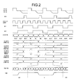
- Fig. 2 is a timing chart of output timings of each signal shown in Fig. 1.
- DRO, DGO, and DBO respectively represents a R signal, a G signal, and a B signal in a 10-bit image data DO.
- This configuration enables low-amplitude differential output and long-distance transmission and high-pixel rate transmission without adding components.
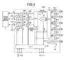
- Fig. 3 is a schematic block diagram of an analog signal processor according to a second embodiment of the present invention.
- the analog signal processor according to the second embodiment includes an analog signal processing IC 1002.
- digital data for each color is n-multiplexed with regard to time and is transmitted at an n-fold data rate. That is, unlike the analog signal processing IC 1001, in the analog signal processing IC 1002, an operation clock of the LVDS block 18 is obtained from the MAP block 17 and an operation is performed by taking a clock CLK that corresponds to a two-fold pixel rate as a reference in the same configuration as in Fig. 2.
- the other components are constituted and function in the same manner as in the analog signal processing IC 1001 so that the explanation thereof is omitted.
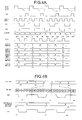
- image data is output twice in a period of one pixel by repeating low-amplitude differential signals TXA to TXE.
- a transmission clock TXCK that corresponds to two cycles in a period of one pixel is output.
- Receiver output in Fig. 4B indicates output timing of parallel signals output by a receiver (not shown) arranged to the rear of the analog signal processing IC 1002.
- each component that is not particularly explained is constituted and functions in the same manner as in the analog signal processor of the first embodiment.
- This configuration makes it possible to make transmission frequencies of low-amplitude differential signals high based on n-multiplexed image data. Therefore, in the case of a low pixel rate, it is possible to reduce effects of low limits in operation frequencies from the receiver shown in the timing chart of Fig. 4B.
- Fig. 5 is a schematic block diagram of an analog signal processor according to a third embodiment of the present invention.
- the analog signal processor according to the third embodiment includes an analog signal processing IC 1003.Clocks that correspond to digital data for each color and digital data rates for each color are serialized, a plurality of serial signals are generated, and they are converted to low-amplitude differential signals, which are output as a plurality of serial low-amplitude differential signals.
- the third embodiment has almost the same configuration as in the second embodiment except that a latch clock CLK 2 for latching output of low-amplitude differential signals from a receiver is embedded in low-amplitude differential signals and is transmitted together with image data.
- Figs. 6A and 6B are timing charts for indicating output timings of each signal in the analog signal processor. As shown in Figs. 6A and 6B, receiver output CK is output based on the CLK 2.
- each component that is not particularly explained is constituted and functions in the same manner as in the first and second embodiments.
- This configuration enables, in addition to effects of the first and second embodiments, because of transmission of image data and identification signals for multiplexing and restoring separation, easy multiplexing and restoring separation based on the identification signals as well as controlling increasing costs accompanied by multiplexing and separation to a minimum.
- Fig. 7 is a schematic block diagram of an analog signal processor according to a fourth embodiment of the present invention.
- the analog signal processor according to the fourth embodiment includes an analog signal processing IC 1004.
- analog signal processing IC 1004 digital data for each color is separated into a plurality of groups of n-bits, is converted to time-division data in sequence, and is transmitted at an n-fold data rate as a plurality of serial low-amplitude differential signals.
- the fourth embodiment has almost the same configuration as in the second embodiment except three data outputs of DA, DB, DC from the MAP 17 block.
- the MAP 17 block that is, point sequential image data sent from the ADC 15 is resolved into data for each color.
- the data is separated into a high-order bit group and a low-order bit group for each color and is output as DA, DB, DC in the order of the high-order bit group to the low-order bit group in time sequence.
- DA, DB, DC have 7 bits respectively.
- the high-order bit group and the low-order bit group for each color have 5 bits respectively and the other bits are occupied by "0" or "1". They are output as three-sequence low-amplitude differential signals from the LVDS 18 block.
- Figs. 8A and 8B are timing charts for indicating output timing of each signal in the analog signal processor.
- each component that is not particularly explained is constituted and functions in the same manner as in the first and second embodiments.
- This configuration enables, in addition to effects of the first and second embodiments, reduction of the number of transmission lines that are required because image data is separated into bit groups and is transmitted in time division as low-amplitude differential signals. As a result, this makes it possible to lead to low costs.
- Fig. 9 is a schematic block diagram of an analog signal processor according to a fifth embodiment of the present invention.
- the analog signal processor according to the fifth embodiment includes an analog signal processing IC 1005.
- the analog signal processing IC 1005 latch clocks or identification signals that each indicate n plural-bit groups into which digital data for each color is separated are converted to low-amplitude differential signals with digital data for each color and are output as plural serial low-amplitude differential signals.
- the fifth embodiment has almost the same configuration as in the fourth embodiment.
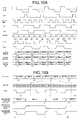
- a signal HEN that indicates a high-order bit group of low-amplitude differential signals output from a receiver is embedded in the low-amplitude differential signals and is transmitted concurrently with image data.
- Figs. 10A and 10B are timing charts for indicating output timing of each signal in the analog signal processor.
- each component that is not particularly explained is constituted and functions in the same manner as in the fourth embodiment.
- This configuration enables, in addition to effects of the fourth embodiment, because of transmission of image data and identification signals for multiplexing and restoring separation, easy multiplexing and restoring separation as well as controlling increasing costs accompanied by multiplexing and separation to a minimum.
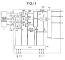
- Fig. 11 is a schematic block diagram of an analog signal processor according to a sixth embodiment of the present invention.
- the analog signal processor according to the sixth embodiment includes an analog signal processing IC 1006.
- analog signal processing IC 1006 digital data for each color is separated into plural bit groups and a multiple-bit parallel output is sequentially performed in time division.
- Point sequential image data DO[9:0] output from the ADC 15 is resolved for each color in the MAP 17 block and furthermore is separated into a high-order bit group and a low-order bit group for each color.
- the data is output in time sequence in the order of a high-order bit group to a low-order bit group as each 5-bit data of DA'[4:0], DB'[4:0], DC'[4:0].
- a clock CLK to latch a high-order bit group and a low-order bit group is also output at the same time in the MAP 17 block.
- Fig. 12 is a timing chart for indicating output timing of each signal in the analog signal processor.
- each component that is not particularly explained is constituted and functions in the same manner as in the fifth embodiment.
- This configuration enables large reduction of the number of signals at a low-pixel rate and in short-distance transmission because data is separated for each color, is separated into plural bit groups, and is transmitted in time division. Compared with point sequential image data transmission, it is possible to simplify restoring processing.
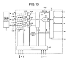
- Fig. 13 is a schematic block diagram of an analog signal processor according to a seventh embodiment of the present invention.
- the analog signal processor according to the seventh embodiment includes an analog signal processing IC 1007.
- analog signal processing IC 1007 digital data that is separated for each color and for each of plural bit groups and is sequentially subjected to multiple-bit parallel output in time division is output with a latch clock or an identification signal that corresponds to each of plural-bit groups.
- Fig. 14 is a timing chart for indicating output timing of each signal in the analog signal processor.
- each component that is not particularly explained is constituted and functions in the same manner as in the sixth embodiment.
- This configuration makes it possible, in addition to effects of the sixth embodiment, to easily restore separated bit groups because image data is separated for each color and separated into plural bit groups and a bit-group identification signal is added thereto.
- Fig. 15 is a schematic block diagram of an analog signal processor according to an eighth embodiment of the present invention.
- the analog signal processor according to the eighth embodiment includes an analog signal processing IC 1008.
- the analog signal processing IC 1008 is a combination of configurations of the analog signal processing IC 1001 and the analog signal processing IC 1006.
- the analog signal processor 1008 includes output terminals for low-amplitude differential signal outputs TXA to TXE, TXCK, parallel outputs DA', DB', DC', a high-order bit group identification signal HEN, and a high-order/low-order bit group latch clock CLK and a switching terminal LVEN for an output mode.
- Fig. 16 is a timing chart for indicating output timing of each signal in the analog signal processor when the switching terminal LVEN of an output mode is "H”.
- Fig. 17 is a timing chart for indicating output timing of each signal in the analog signal processor when the switching terminal LVEN of an output mode is "L”.
- each component that is not particularly explained is constituted and functions in the same manner as in the first and sixth embodiments.
- This configuration makes it possible to perform data transmission that matches a system at low costs because of a function of performing both of low-amplitude differential transmission and parallel transmission.
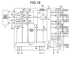
- Fig. 18 is a schematic block diagram of an analog signal processor according to a ninth embodiment of the present invention.
- the analog signal processor according to the ninth embodiment includes an analog signal processing IC 1009.
- the analog signal processing IC 1009 low-amplitude differential signal outputs TXA to TXE, TXCK and parallel outputs DA' to DC', HEN, and CLK are in common with one terminal respectively unlike the circuit of the eighth embodiment.
- output terminals for low-amplitude differential signals TXA to TXE, TXCK are valid and parallel outputs DA' to DC', HEN, CLK are at high impedance or H/L fixed output.
- parallel outputs DA' to DC', HEN, CLK are valid and low-amplitude differential signals TXA to TXE, TXCK are at high impedance or H/L fixed output.
- Fig. 19 is a timing chart for indicating output timing of each signal in the analog signal processor in the low-amplitude differential signal output mode.
- Fig. 20 is a timing chart for indicating output timing of each signal in the analog signal processor in the parallel output mode.
- each component that is not particularly explained is constituted and functions in the same manner as in the eighth embodiment.
- This configuration enables, in addition to effects of the eighth embodiment, implementation of low-amplitude differential signal transmission and parallel transmission with a small number of terminals and compact-size and low-cost signal processing IC.
- Fig. 21 is a schematic side view of an image reading apparatus according to a ninth embodiment of the present invention.
- the image reading apparatus is a scanner, for example, that is connected to a personal computer (PC) or mounted on a color digital copier.
- PC personal computer
- a document image is read by the color linear image sensor 1 and processed by converting image signals to digital signals.
- the image reading apparatus includes a contact glass 101 on which a document sheet 112 is placed, a first carriage 106 on which a halogen lamp 102 for exposing documents and a first reflection mirror 103 are mounted, a second carriage 107 on which a second reflection mirror 104 and a third reflection mirror 105 are mounted, the color linear image sensor 1 for performing photoelectric conversion to incident light, a lens unit 108 for forming an image on the color linear image sensor 1 through reading light incident from the third mirror 105, and a white reference plate 113 that is arranged at the top of a scanner 100 to correct various distortions caused by a reading optical system.
- the color linear image sensor 1 is mounted on a sensor board unit 110 and predetermined processing is performed to signals to which photoelectric conversion is performed by the color linear image sensor 1 on the sensor board unit 110. That is, any of the analog signal processing ICs 1001 to 1008 can be mounted on the sensor board unit 110.
- the first carriage 106 and the second carriage 107 are moved by a stepping motor (not shown) at a speed ratio of two to one along a rail (not shown) in a sub-scanning direction A and read document sheets.
- Fig. 22 is a schematic side view of the whole tandem image forming apparatus on which the image reading apparatus shown in Fig. 21 is mounted.
- the image forming apparatus basically includes a paper feeder PS, the image forming apparatus body PR, a scanner (a document reading apparatus) 100, and an automatic document feeder (ADF).
- the image forming apparatus body PR includes a tandem image forming unit 50, resist rollers 52 for supplying recording paper through a transmission path 51 from the paper feeder PS to the image forming unit 50, an optical writing device 57, a fixing/transmitting unit 58, and a two-side tray 59.
- the image forming unit 50 includes four photoconductor drums 54 arranged in parallel with one another, each of which corresponds to four colors of YMCK.
- the image forming unit 50 also includes image forming components, such as a charger, a developing device 55, a transfer device, a cleaner, and a static eliminator. Moreover, an intermediate transfer belt 53 is laid across in a tensioned condition between a driving roller and a driven roller while sandwiched in a nip between the transfer device and the photoconductor drum 54.
- optical writing is performed to the photoconductor drums 54, each of which corresponds to each color of YMCK.
- An image on the photoconductor drum 54 is developed for each color of toners by the developing device 55 and a first transfer is performed on the intermediate transfer belt 53, for example, in the order of Y, M, C, K.
- a full-color image on which four colors are superimposed through the first transfer is subjected to a second transfer on recording paper, then fixed, and the resulting paper is discharged, thereby forming the full-color image on the recording paper.
- a color linear image sensor corresponds to a reference numeral 1
- a unit for sampling and holding corresponds to sample-hold circuits 12R, 12G, 12B
- a unit for amplifying corresponds to variable gain amplifiers 13R, 13G, 13B
- a unit for analog-digital conversion corresponds to an analog-digital converter 15
- a unit for outputting as a plurality of serial low-amplitude differential signals corresponds to a MAP 17 and LVDSs 18-1 to 18-6
- a unit for multiple-bit parallel output corresponds to the MAP 17
- an image reading apparatus corresponds to a reference numeral 100
- an image forming apparatus corresponds to a reference sign PR.
- the read signal processor forms images as described above or functions as a first stage when capturing an image on a personal computer (PC).
- PC personal computer
- the read signal processor includes a unit that outputs as a plurality of serial low-amplitude differential signals or a unit that sequentially performs multiple-bit parallel output in time division.
Landscapes
- Engineering & Computer Science (AREA)
- Multimedia (AREA)
- Signal Processing (AREA)
- Facsimile Heads (AREA)
- Facsimile Scanning Arrangements (AREA)
- Image Input (AREA)
- Facsimile Image Signal Circuits (AREA)
Applications Claiming Priority (1)
| Application Number | Priority Date | Filing Date | Title |
|---|---|---|---|
| JP2006253189A JP4594911B2 (ja) | 2006-09-19 | 2006-09-19 | 読み取り信号処理装置、画像読み取り装置、及び画像形成装置 |
Publications (3)
| Publication Number | Publication Date |
|---|---|
| EP1903804A2 true EP1903804A2 (de) | 2008-03-26 |
| EP1903804A3 EP1903804A3 (de) | 2012-04-04 |
| EP1903804B1 EP1903804B1 (de) | 2015-04-08 |
Family
ID=38608914
Family Applications (1)
| Application Number | Title | Priority Date | Filing Date |
|---|---|---|---|
| EP07253517.2A Ceased EP1903804B1 (de) | 2006-09-19 | 2007-09-05 | Lesesignalprozessor, Bildlesevorrichtung und Bilderzeugungsvorrichtung |
Country Status (3)
| Country | Link |
|---|---|
| US (1) | US8081100B2 (de) |
| EP (1) | EP1903804B1 (de) |
| JP (1) | JP4594911B2 (de) |
Cited By (2)
| Publication number | Priority date | Publication date | Assignee | Title |
|---|---|---|---|---|
| EP2362630A1 (de) * | 2010-02-26 | 2011-08-31 | Brother Kogyo Kabushiki Kaisha | Bildleser |
| US8576461B2 (en) | 2010-02-26 | 2013-11-05 | Brother Kogyo Kabushiki Kaisha | Image reader |
Families Citing this family (16)
| Publication number | Priority date | Publication date | Assignee | Title |
|---|---|---|---|---|
| JP4699417B2 (ja) * | 2007-04-16 | 2011-06-08 | 株式会社リコー | アナログ処理回路およびアナログ集積回路装置および画像読取装置および画像形成装置 |
| US8264747B2 (en) * | 2007-05-28 | 2012-09-11 | Ricoh Company, Ltd. | Image reading device and image reading method |
| US8305663B2 (en) | 2007-09-05 | 2012-11-06 | Ricoh Company, Limited | Signal generator, image reading device, and image forming apparatus |
| US7965121B2 (en) * | 2008-01-03 | 2011-06-21 | Mediatek Inc. | Multifunctional output drivers and multifunctional transmitters using the same |
| JP4974930B2 (ja) * | 2008-02-27 | 2012-07-11 | 株式会社リコー | タイミング信号発生器及びそれを備えた画像読取装置 |
| US8179984B2 (en) * | 2008-11-12 | 2012-05-15 | Mediatek Inc. | Multifunctional transmitters |
| JP6549366B2 (ja) | 2014-09-19 | 2019-07-24 | 株式会社リコー | 光電変換素子、画像読取装置及び画像形成装置 |
| JP6612492B2 (ja) | 2014-10-16 | 2019-11-27 | 株式会社リコー | 光電変換素子、画像読取装置及び画像形成装置 |
| KR102355023B1 (ko) * | 2015-03-30 | 2022-01-25 | 엘지이노텍 주식회사 | 인쇄회로기판 |
| JP6700673B2 (ja) * | 2015-05-15 | 2020-05-27 | キヤノン株式会社 | 撮像装置、撮像システム |
| JP6556001B2 (ja) | 2015-09-24 | 2019-08-07 | キヤノン株式会社 | 画像読取装置 |
| EP3432565B1 (de) | 2016-03-16 | 2020-07-08 | Ricoh Company, Ltd. | Photoelektrische umwandlungsvorrichtung, bildlesevorrichtung und bilderzeugungsvorrichtung |
| JP6862921B2 (ja) | 2017-03-01 | 2021-04-21 | 株式会社リコー | アナログ信号バス駆動回路、及び光電変換装置 |
| WO2019065393A1 (ja) * | 2017-09-29 | 2019-04-04 | キヤノン株式会社 | 撮像素子及び撮像装置 |
| JP7476523B2 (ja) | 2019-11-25 | 2024-05-01 | 株式会社リコー | 信号処理装置、撮像装置、読取装置、画像形成装置および信号処理方法 |
| CN112187362B (zh) * | 2020-08-21 | 2021-09-07 | 北京航天时代光电科技有限公司 | 一种兼容多种通信接口的光电传输板卡 |
Citations (1)
| Publication number | Priority date | Publication date | Assignee | Title |
|---|---|---|---|---|
| US20060176201A1 (en) | 2005-02-10 | 2006-08-10 | Seiko Epson Corporation | Analog front-end circuit and electronic device |
Family Cites Families (20)
| Publication number | Priority date | Publication date | Assignee | Title |
|---|---|---|---|---|
| US5408113A (en) | 1992-06-30 | 1995-04-18 | Ricoh Company, Ltd. | High sensitivity improved photoelectric imaging device with a high signal to noise ratio |
| FR2755324B1 (fr) * | 1996-10-25 | 1999-01-08 | Thomson Multimedia Sa | Conversion d'un signal analogique en signal numerique en particulier un signal video de tv |
| JPH10304190A (ja) | 1997-04-23 | 1998-11-13 | Ricoh Co Ltd | 画像形成装置 |
| JPH10304135A (ja) * | 1997-04-28 | 1998-11-13 | Fuji Photo Film Co Ltd | A/d変換データ時分割伝送回路 |
| JPH10319919A (ja) | 1997-05-21 | 1998-12-04 | Sharp Corp | 表示画像データ伝送方式及びその信号処理用ic |
| JPH11122407A (ja) * | 1997-10-17 | 1999-04-30 | Ricoh Co Ltd | 画像処理装置 |
| JP3653171B2 (ja) | 1998-03-09 | 2005-05-25 | 株式会社リコー | 可変ゲイン増幅装置 |
| JP3715859B2 (ja) * | 2000-02-03 | 2005-11-16 | キヤノン株式会社 | システム |
| JP3744301B2 (ja) * | 2000-02-14 | 2006-02-08 | コニカミノルタビジネステクノロジーズ株式会社 | 画像読み取り装置 |
| JP2001255841A (ja) | 2000-03-09 | 2001-09-21 | Matsushita Electric Ind Co Ltd | 表示装置及びその駆動回路と信号伝送方法 |
| JP2002199213A (ja) | 2000-12-27 | 2002-07-12 | Ricoh Co Ltd | 画像読取装置 |
| JP2002281325A (ja) | 2001-03-19 | 2002-09-27 | Ricoh Co Ltd | カラー画像読取装置 |
| JP4672168B2 (ja) * | 2001-04-03 | 2011-04-20 | 東芝モバイルディスプレイ株式会社 | データ処理システム |
| JP2004048265A (ja) | 2002-07-10 | 2004-02-12 | Ricoh Co Ltd | 原稿読み取り装置および画像形成装置 |
| JP2004072344A (ja) | 2002-08-05 | 2004-03-04 | Ricoh Co Ltd | 多重化lvdsインタフェースを備えたデータ伝送システム |
| JP2005012752A (ja) | 2003-02-26 | 2005-01-13 | Seiko Instruments Inc | 信号処理回路、イメージセンサーicおよび信号処理方法 |
| US7154495B1 (en) * | 2003-12-01 | 2006-12-26 | Analog Devices, Inc. | Analog interface structures and methods for digital displays |
| JP4412070B2 (ja) * | 2004-06-24 | 2010-02-10 | 富士ゼロックス株式会社 | 画像読み取り装置、画像データの補正方法 |
| US7480012B1 (en) * | 2005-02-24 | 2009-01-20 | Pixelworks, Inc. | Multiplexed video digitization system and method |
| US7382298B1 (en) * | 2007-01-17 | 2008-06-03 | Analog Devices, Inc. | Code-correction structures and methods for digital displays |
-
2006
- 2006-09-19 JP JP2006253189A patent/JP4594911B2/ja not_active Expired - Fee Related
-
2007
- 2007-09-05 EP EP07253517.2A patent/EP1903804B1/de not_active Ceased
- 2007-09-07 US US11/851,657 patent/US8081100B2/en active Active
Patent Citations (1)
| Publication number | Priority date | Publication date | Assignee | Title |
|---|---|---|---|---|
| US20060176201A1 (en) | 2005-02-10 | 2006-08-10 | Seiko Epson Corporation | Analog front-end circuit and electronic device |
Cited By (5)
| Publication number | Priority date | Publication date | Assignee | Title |
|---|---|---|---|---|
| EP2362630A1 (de) * | 2010-02-26 | 2011-08-31 | Brother Kogyo Kabushiki Kaisha | Bildleser |
| US8576461B2 (en) | 2010-02-26 | 2013-11-05 | Brother Kogyo Kabushiki Kaisha | Image reader |
| US8593702B2 (en) | 2010-02-26 | 2013-11-26 | Brother Kogyo Kabushiki Kaisha | Image reader |
| US8837013B2 (en) | 2010-02-26 | 2014-09-16 | Brother Kogyo Kabushiki Kaisha | Image reader |
| US9344594B2 (en) | 2010-02-26 | 2016-05-17 | Brother Kogyo Kabushiki Kaisha | Image reader |
Also Published As
| Publication number | Publication date |
|---|---|
| EP1903804A3 (de) | 2012-04-04 |
| US8081100B2 (en) | 2011-12-20 |
| US20080068683A1 (en) | 2008-03-20 |
| JP4594911B2 (ja) | 2010-12-08 |
| JP2008078796A (ja) | 2008-04-03 |
| EP1903804B1 (de) | 2015-04-08 |
Similar Documents
| Publication | Publication Date | Title |
|---|---|---|
| US8081100B2 (en) | Read signal processor, image reading apparatus, and image forming apparatus | |
| US8395830B2 (en) | Image reading signal processing IC, image reading apparatus, and image forming apparatus | |
| USRE42742E1 (en) | Image inputting apparatus and image forming apparatus using four-line CCD sensor | |
| US8212908B2 (en) | Timing generator and image scanning apparatus | |
| JP3667001B2 (ja) | 画像処理装置及びその方法 | |
| JP2016116089A (ja) | 光電変換素子、画像読取装置及び画像形成装置 | |
| US8610805B2 (en) | Electronic device with an array of daisy chained image sensors and associated methods | |
| JP4446674B2 (ja) | 画像処理装置及び撮像装置 | |
| US7610419B2 (en) | Data transmission apparatus, data reception apparatus, data transmission and reception apparatus and data transmission and reception method | |
| JPH03285459A (ja) | 画像読取装置 | |
| JP5275312B2 (ja) | イメージセンサモジュール及びイメージセンサ | |
| JP2009272891A (ja) | 画像読取装置、画像形成装置、画像読取方法及び画像形成方法 | |
| JPH10304133A (ja) | 相関二重サンプリング回路 | |
| EP2552117A2 (de) | Fotoelektrischer Wandler, Bildlesevorrichtung und Bildleseverfahren | |
| US20070070444A1 (en) | Image reading apparatus and image forming apparatus | |
| JP2015159438A (ja) | 撮像素子、画像読取装置及び画像形成装置 | |
| JP5115888B2 (ja) | 画像処理装置及び撮像装置 | |
| JP3846670B2 (ja) | 画像読取装置 | |
| US20080174840A1 (en) | Methods and apparatuses for changing driving sequence to output charge coupled device signal | |
| US7893977B2 (en) | Multiplexing and offset correction system for an image sensor array | |
| JP5469197B2 (ja) | 画像処理システムおよび撮像装置 | |
| JPH11164088A (ja) | 固体撮像素子およびこれを備えた画像読取装置 | |
| JP2004112530A (ja) | 画像処理装置、画像読取装置、複写機、ファクシミリ装置及び画像読取装置の製造方法 | |
| US20120008157A1 (en) | Image forming apparatus and network system | |
| JP2002218256A (ja) | カラー画像読取装置およびカラー画像読取装置における画像読取方法 |
Legal Events
| Date | Code | Title | Description |
|---|---|---|---|
| PUAI | Public reference made under article 153(3) epc to a published international application that has entered the european phase |
Free format text: ORIGINAL CODE: 0009012 |
|
| AK | Designated contracting states |
Kind code of ref document: A2 Designated state(s): AT BE BG CH CY CZ DE DK EE ES FI FR GB GR HU IE IS IT LI LT LU LV MC MT NL PL PT RO SE SI SK TR |
|
| AX | Request for extension of the european patent |
Extension state: AL BA HR MK YU |
|
| RIC1 | Information provided on ipc code assigned before grant |
Ipc: H04N 9/04 20060101AFI20111020BHEP |
|
| PUAL | Search report despatched |
Free format text: ORIGINAL CODE: 0009013 |
|
| RIC1 | Information provided on ipc code assigned before grant |
Ipc: H04N 9/04 20060101AFI20120223BHEP |
|
| AK | Designated contracting states |
Kind code of ref document: A3 Designated state(s): AT BE BG CH CY CZ DE DK EE ES FI FR GB GR HU IE IS IT LI LT LU LV MC MT NL PL PT RO SE SI SK TR |
|
| AX | Request for extension of the european patent |
Extension state: AL BA HR MK RS |
|
| 17P | Request for examination filed |
Effective date: 20120821 |
|
| 17Q | First examination report despatched |
Effective date: 20121011 |
|
| AKX | Designation fees paid |
Designated state(s): DE FR GB |
|
| GRAP | Despatch of communication of intention to grant a patent |
Free format text: ORIGINAL CODE: EPIDOSNIGR1 |
|
| INTG | Intention to grant announced |
Effective date: 20141024 |
|
| GRAS | Grant fee paid |
Free format text: ORIGINAL CODE: EPIDOSNIGR3 |
|
| GRAA | (expected) grant |
Free format text: ORIGINAL CODE: 0009210 |
|
| AK | Designated contracting states |
Kind code of ref document: B1 Designated state(s): DE FR GB |
|
| REG | Reference to a national code |
Ref country code: GB Ref legal event code: FG4D |
|
| REG | Reference to a national code |
Ref country code: DE Ref legal event code: R096 Ref document number: 602007040943 Country of ref document: DE Effective date: 20150521 |
|
| REG | Reference to a national code |
Ref country code: DE Ref legal event code: R097 Ref document number: 602007040943 Country of ref document: DE |
|
| PLBE | No opposition filed within time limit |
Free format text: ORIGINAL CODE: 0009261 |
|
| STAA | Information on the status of an ep patent application or granted ep patent |
Free format text: STATUS: NO OPPOSITION FILED WITHIN TIME LIMIT |
|
| 26N | No opposition filed |
Effective date: 20160111 |
|
| REG | Reference to a national code |
Ref country code: FR Ref legal event code: PLFP Year of fee payment: 10 |
|
| REG | Reference to a national code |
Ref country code: FR Ref legal event code: PLFP Year of fee payment: 11 |
|
| REG | Reference to a national code |
Ref country code: FR Ref legal event code: PLFP Year of fee payment: 12 |
|
| PGFP | Annual fee paid to national office [announced via postgrant information from national office to epo] |
Ref country code: FR Payment date: 20200914 Year of fee payment: 14 Ref country code: DE Payment date: 20200925 Year of fee payment: 14 Ref country code: GB Payment date: 20200922 Year of fee payment: 14 |
|
| REG | Reference to a national code |
Ref country code: DE Ref legal event code: R119 Ref document number: 602007040943 Country of ref document: DE |
|
| GBPC | Gb: european patent ceased through non-payment of renewal fee |
Effective date: 20210905 |
|
| PG25 | Lapsed in a contracting state [announced via postgrant information from national office to epo] |
Ref country code: GB Free format text: LAPSE BECAUSE OF NON-PAYMENT OF DUE FEES Effective date: 20210905 Ref country code: FR Free format text: LAPSE BECAUSE OF NON-PAYMENT OF DUE FEES Effective date: 20210930 Ref country code: DE Free format text: LAPSE BECAUSE OF NON-PAYMENT OF DUE FEES Effective date: 20220401 |