EP1897128B1 - Passivierung von auf grossem bandabstand basierenden halbleiterbauelementen mit wasserstofffreien gesputterten nitriden - Google Patents
Passivierung von auf grossem bandabstand basierenden halbleiterbauelementen mit wasserstofffreien gesputterten nitriden Download PDFInfo
- Publication number
- EP1897128B1 EP1897128B1 EP06785888.6A EP06785888A EP1897128B1 EP 1897128 B1 EP1897128 B1 EP 1897128B1 EP 06785888 A EP06785888 A EP 06785888A EP 1897128 B1 EP1897128 B1 EP 1897128B1
- Authority
- EP
- European Patent Office
- Prior art keywords
- layer
- stoichiometric
- silicon nitride
- silicon
- passivated
- Prior art date
- Legal status (The legal status is an assumption and is not a legal conclusion. Google has not performed a legal analysis and makes no representation as to the accuracy of the status listed.)
- Active
Links
Images

Classifications
-
- H—ELECTRICITY
- H10—SEMICONDUCTOR DEVICES; ELECTRIC SOLID-STATE DEVICES NOT OTHERWISE PROVIDED FOR
- H10D—INORGANIC ELECTRIC SEMICONDUCTOR DEVICES
- H10D62/00—Semiconductor bodies, or regions thereof, of devices having potential barriers
- H10D62/80—Semiconductor bodies, or regions thereof, of devices having potential barriers characterised by the materials
- H10D62/83—Semiconductor bodies, or regions thereof, of devices having potential barriers characterised by the materials being Group IV materials, e.g. B-doped Si or undoped Ge
- H10D62/832—Semiconductor bodies, or regions thereof, of devices having potential barriers characterised by the materials being Group IV materials, e.g. B-doped Si or undoped Ge being Group IV materials comprising two or more elements, e.g. SiGe
- H10D62/8325—Silicon carbide
-
- H—ELECTRICITY
- H10—SEMICONDUCTOR DEVICES; ELECTRIC SOLID-STATE DEVICES NOT OTHERWISE PROVIDED FOR
- H10D—INORGANIC ELECTRIC SEMICONDUCTOR DEVICES
- H10D62/00—Semiconductor bodies, or regions thereof, of devices having potential barriers
- H10D62/80—Semiconductor bodies, or regions thereof, of devices having potential barriers characterised by the materials
-
- H—ELECTRICITY
- H10—SEMICONDUCTOR DEVICES; ELECTRIC SOLID-STATE DEVICES NOT OTHERWISE PROVIDED FOR
- H10P—GENERIC PROCESSES OR APPARATUS FOR THE MANUFACTURE OR TREATMENT OF DEVICES COVERED BY CLASS H10
- H10P14/00—Formation of materials, e.g. in the shape of layers or pillars
- H10P14/60—Formation of materials, e.g. in the shape of layers or pillars of insulating materials
- H10P14/63—Formation of materials, e.g. in the shape of layers or pillars of insulating materials characterised by the formation processes
- H10P14/6326—Deposition processes
- H10P14/6328—Deposition from the gas or vapour phase
-
- H—ELECTRICITY
- H10—SEMICONDUCTOR DEVICES; ELECTRIC SOLID-STATE DEVICES NOT OTHERWISE PROVIDED FOR
- H10P—GENERIC PROCESSES OR APPARATUS FOR THE MANUFACTURE OR TREATMENT OF DEVICES COVERED BY CLASS H10
- H10P14/00—Formation of materials, e.g. in the shape of layers or pillars
- H10P14/60—Formation of materials, e.g. in the shape of layers or pillars of insulating materials
- H10P14/69—Inorganic materials
- H10P14/694—Inorganic materials composed of nitrides
- H10P14/6943—Inorganic materials composed of nitrides containing silicon
- H10P14/69433—Inorganic materials composed of nitrides containing silicon the material being a silicon nitride not containing oxygen, e.g. SixNy or SixByNz
-
- H—ELECTRICITY
- H10—SEMICONDUCTOR DEVICES; ELECTRIC SOLID-STATE DEVICES NOT OTHERWISE PROVIDED FOR
- H10D—INORGANIC ELECTRIC SEMICONDUCTOR DEVICES
- H10D62/00—Semiconductor bodies, or regions thereof, of devices having potential barriers
- H10D62/80—Semiconductor bodies, or regions thereof, of devices having potential barriers characterised by the materials
- H10D62/85—Semiconductor bodies, or regions thereof, of devices having potential barriers characterised by the materials being Group III-V materials, e.g. GaAs
- H10D62/8503—Nitride Group III-V materials, e.g. AlN or GaN
Definitions
- the present invention relates to semiconductor structures and devices formed in wide bandgap materials such as silicon carbide and the Group III nitrides.
- semiconductor devices fundamentally depend upon the inherent properties of the semiconductor materials from which they are made, as well as the extent to which these materials can be incorporated in a useful device structure. Semiconductor devices also depend upon the manner in which various semiconductor materials are formed and arranged with respect to one another.
- One of the characteristics of semiconductor materials is their bandgap; i.e., the energy difference between the valence band of electrons and the conductance band.
- the size of the material's bandgap provides fundamental limitations upon-or possibilities for-device structures and performances.
- microwave systems-typical examples of which include cellular communications systems -commonly use solid state transistors as amplifiers and oscillators.
- solid state transistors as amplifiers and oscillators.
- Higher frequency signals can carry more information (bandwidth), allow for smaller antennas with very high gain, and provide systems such as radar with improved resolution.
- wide bandgap materials such as silicon carbide (SiC) and the Group III (Ga, Al, In) nitrides have been, and continue to be, materials of significant interest for high frequency devices.
- Higher bandgap materials also offer the potential for higher power capabilities (as compared to similar structures made from smaller bandgap materials) as well as the potential for emitting light at higher frequencies; e.g., the green, blue, violet and ultraviolet portions of the electromagnetic spectrum.
- Devices fabricated from silicon carbide are typically passivated with an oxide layer, such as SiO 2 , to protect the exposed SiC surfaces of the device, or for other reasons, or both.
- oxide layer such as SiO 2
- the interface between SiC and SiO 2 may be insufficient to obtain a high surface mobility of electrons. More specifically, the interface between SiC and SiO 2 conventionally exhibits a high density of interface states, which may reduce surface electron mobility and introduce carrier traps, which in turn reduces the desired performance characteristics of devices such as (but not limited to) metal-oxide-semiconductor field-effect transistors (MOSFETs).
- MOSFETs metal-oxide-semiconductor field-effect transistors
- semiconductor devices including those that include oxidation layers, also incorporate one or more layers of silicon nitride to improve the resulting electronic properties (e.g., U.S. Patent No. 6,246,076 ).
- Silicon nitride also provides an environmental barrier that the oxide fails to provide, or without which, would allow the environment to degrade the structure and operation of the device, regardless of whether the device includes an oxide layer.
- silicon nitride is preferred over silicon dioxide because it forms a better seal over the device, preventing contaminants such as water from reaching the epitaxial layers of the device and from causing degradation.
- Silicon nitride may also be used to form layers that transmit light generated within an LED.
- nitride does not provide the open channels found in oxide structures; thus, nitride is widely employed in electronics as a barrier material.
- hydrogen diffuses slowly in a densified nitride film, and other small positive ions (Na + or K + ) are effectively blocked by thin nitride layers. Because oxygen diffuses very slowly through nitride, deposited nitride can prevent oxidation of underlying silicon.
- nitrides deposited using chemical vapor deposition almost always contain hydrogen, typically much more than in the comparable oxide films.
- the source of the hydrogen is the silane precursor and also the ammonia employed in many CVD schemes.
- An amorphous, but constrained, film such as silicon nitride can discourage the atoms from occupying positions that fill the valences of each silicon and nitrogen atom. Thus, many broken bonds tend to be present. These bonds are readily occupied by hydrogen atoms.
- conventional plasma nitrides can have as much as 20 atomic percent hydrogen, bonded both to the Si and N atoms; thermal nitrides still have several percent hydrogen even after high-temperature anneals.
- hydrogen can passivate Mg-acceptors in a GaN-based semiconductor.
- silicon nitride is deposited by means of PECVD at a deposition temperature in excess of 200 °C.
- hydrogen in the film can diffuse through thin ohmic contacts or other layers and into nearby Group III nitride layers, causing them to become passivated in a region close to their surface. That is, in a region near the surface, a substantial number of acceptor ions are rendered neutral by the introduction of hydrogen in the film. Accordingly, an interface between an ohmic contact and a nitride material is degraded, and the contact metal does not exhibit ideal ohmic characteristics. This can result in an increase in forward voltage (V f degradation) in the device. Essentially, the device will behave as though the interface between a metal and a Group III nitride contact layer forms a Schottky contact instead of an ohmic contact.
- nitride passivation layers are often used in conjunction with oxide layers, the hydrogen can migrate to the oxide layers.
- hydrogen in oxide films on SiC has been shown to alter the interface Fermi level and encourage a state of surface accumulation. Any resulting accumulation layer produces a charge layer that alters the device capacitance and exhibits a drift with a long time constant caused by the mobility of the hydrogen in the film.
- oxide and nitride layers offer certain advantages, they also raise certain problems that can limit or degrade device performance.
- Document US 2003/0025121 A1 discloses a light emitting diode that offers high-reliability in standard packaging and that will withstand high temperature and high humidity conditions.
- the diode comprises a Group III nitride heterojunction diode with a p-type Group III nitride contact layer, an ohmic contact to the p-type contact layer, and a sputter-deposited silicon nitride composition passivation layer on the ohmic contact.
- a method of manufacturing a light emitting diode and an LED lamp incorporating the diode are also disclosed.
- the present invention provides a structure as detailed in claim 1, a device according to claim 9, and a method in accordance with claim 11.
- Advantageous features are provided in dependent claims.
- the invention is a passivated semiconductor structure and resulting passivated semiconductor devices.
- the invention can be broadly considered as a two part structure in which a chemical vapor deposited passivation layer of silicon nitride encapsulates a previously sputtered-deposited layer of silicon nitride.
- the sputtered layer provides some of the benefits of passivation and the chemical vapor deposited layer provides an excellent environmental barrier.
- the invention is a two-part structure formed of a stoichiometric layer of silicon nitride deposited upon a non-stoichiometric layer of silicon nitride.
- the non-stoichiometric layer enhances the electronic properties of the structure or resulting device and the stoichiometric layer provides an excellent environmental barrier.
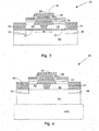
- FIG. 1 shows a semiconductor structure broadly designated at 10 in cross sectional schematic fashion.
- the structure includes a silicon carbide substrate (or layer) 11 with an oxidation layer 12, typically a thermally-generated layer of silicon dioxide, on the silicon carbide substrate 11.
- an oxidation layer 12 typically a thermally-generated layer of silicon dioxide
- substrate 11 is descriptive and explanatory of the silicon carbide portion 11 rather than limiting.
- the silicon carbide substrate 11 can be a wafer or wafer precursor, or can be a functional layer positioned upon other supporting structures (not shown).
- the thermal oxidation layer 12 lowers the interface density between the silicon carbide substrate 1 1 and the thermal oxidation layer 12 and thus enhances the operation of the resulting devices formed from or incorporating the structure 10.
- FIG. 1 shows a sputtered silicon nitride portion 13 and a plasma enhanced chemical vapor deposited (PECVD) layer of silicon nitride 14.
- PECVD plasma enhanced chemical vapor deposited
- FIG. 15 shows the structure broadly designated at 15.
- the structure 15 again includes the silicon carbide substrate 11 and the thermal oxide 12.
- a first sputtered nonstoichiometric layer 16 is on the thermal oxidation layer 12 for reducing parasitic capacitance and minimizing device trapping.
- a second sputtered non-stoichiometric silicon nitride layer 17 is on the first layer 16 for positioning subsequent passivation layers further from the substrate 11, but without fully encapsulating the structure 15.
- a sputtered stoichiometric silicon nitride layer 20 is on the second sputtered nonstoichiometric layer 17 for initially encapsulating the structure 15 and for enhancing the hydrogen barrier properties of the passivation layers.
- the chemical vapor deposited environmental barrier layer again labeled at 14, covers the device to provide step coverage and crack prevention.
- the thermal oxidation layer 12 is stoichiometric silicon dioxide (SiO 2 ) with a thickness in exemplary embodiments of between about 100 and 500 angstroms ( ⁇ ). This is a sufficient thickness to provide the electronic benefits of the oxide (as opposed to a nitride-only passivation), but less than a thickness that would raise additional manufacturing problems.
- sputtering is such that it provides a silicon nitride layer that is substantially hydrogen-free.
- layers 16, 17 and 20 are advantageously substantially hydrogen free.
- the first two sputtered layers 16 and 17 are preferentially nitrogen-rich.
- the proportion of silicon or nitrogen (in a non-stoichiometric composition) can be determined by the refractive index, which is an indicator of the composition of the formed silicon nitride film.
- a silicon nitride film having a substantially stoichiometric composition has a refractive index of 2.02 measured @ 6328 ⁇ .
- Silicon rich nitride has an atomic ratio of silicon to nitrogen that is greater than 3:4 (i.e., stoichiometric silicon nitride is Si 3 N 4 ).
- a typical silicon rich nitride will have an index of refraction of greater than 2.02 measured @6328 ⁇ and a nitrogen rich SiN film will have an index of refraction lower than 2.02 measured @6328 ⁇ .
- each of the nonstoichiometric sputtered silicon nitride layers 16 and 17 have a refractive index of between about 1.85 and 1.95.
- the silicon carbide substrate is often a single crystal and has a polytype selected from the group consisting of the 3C, 4H, 6H and 15R polytypes of silicon carbide.
- sputtering is to avoid the presence of hydrogen as described elsewhere herein, and to correspondingly avoid the electronic problems associated with the presence of hydrogen. Accordingly, the sputtered layers described with respect to Figures 1 and 2 can also be understood as hydrogen-free layers. Stated differently, sputtering is one technique for producing a hydrogen-free passivation layer. The invention, however, can also be understood as the hydrogen free passivation layer regardless of its method of manufacture.
- Figures 3 and 4 illustrate the invention in the context of respective exemplary devices. It will be understood that the invention is not limited to the illustrated devices or to particular families of devices, but can be incorporated as desired or needed in a wide variety of devices familiar to those of skill in this art.
- FIG 3 illustrates a silicon carbide based device broadly designated at 22.
- the device includes a silicon carbide substrate 23 that has a first conductivity type (i.e., n or p). Respective source 24 and drain regions 25 are formed either in or adjacent the substrate 23, and define a channel region 26 therebetween.
- the device 22 includes a thermal oxide layer 27 as described previously and respective ohmic contacts to the source 30, the drain 31 and as a gate contact 32. Because the nature of the invention in is primarily, although not exclusively, emphasized in the passivation structure, the operation of the device 22, which is otherwise well understood by those of ordinary skill in this art, will not be described in detail herein. Exemplary references for semiconductor devices include Dorf, The Electrical Engineering Handbook, Second Edition (CRC Press 1997), Chapter 39, particularly pages 994-996 ; and Sze, Physics of Semiconductor Devices, Second Edition (John Wiley & Sons, Inc. 1981 ).
- the materials for the ohmic and gate contacts can be selected from a plurality of metals or highly conductive semiconductors and that this can be accomplished without undue experimentation by those of skill in this art.
- a first passivation structure formed of nonstoichiometric silicon nitride is on the thermal oxide 27.
- the first passivation structure reduces parasitic capacitance and minimizes device trapping and positions subsequent passivation layers further from the channel 26.
- the first passivation structure comprises two layers 33 and 34 of sputtered non-stoichiometric silicon nitride on the thermal oxide layer 27.
- the second passivation structure comprises a sputtered-deposited layer 35 of silicon nitride on the first passivation structure, and in particular on the layer 34, and a chemical vapor deposited layer 36 of silicon nitride on the sputter-deposited layer 35.
- both of the layers 35 and 36 comprise stoichiometric silicon nitride.
- the sputtered layers 33 and 34 are advantageously substantially hydrogen free, and similarly because the layer 35 is also sputtered, it is likewise substantially hydrogen free.
- Figure 4 illustrates a device 40 based on gallium nitride (GaN) or aluminum gallium nitride (AlGaN) as the semiconductor.
- the device 40 includes the gallium nitride or aluminum gallium nitride layer 41 and potentially can include an additional substrate or substrate and buffer structure which is designated by the dotted rectangle 42.
- a bulk crystal of gallium nitride can theoretically eliminate the need for the substrate and buffer 42, but most devices of this type will include a substrate of SiC or sapphire or some other suitable material.
- the aluminum gallium nitride is best expressed as Al x Ga 1-x N where 0 ⁇ x ⁇ 1.
- the atomic fractions of aluminum and gallium can be selected as desired or necessary based upon the intended structure and operation of the device
- the device 40 includes the source region 43 and the drain region 44.
- the oxide layer is not present and, as known to those familiar with these materials and structures, neither gallium nitride nor aluminum gallium nitride form a suitable oxide under typical conditions appropriate for semiconductor device manufacture.
- ohmic contacts 46 and 47 are made to the source 43 and drain 44 respectively.
- the device 40 includes the first sputtered silicon nitride or aluminum nitride layer 50 and the second sputtered silicon nitride layer 51, both of which may be non-stoichiometric, hydrogen-free, and have a refractive index of between about 1.85 and 2.05.
- the encapsulating stoichiometric silicon nitride layer is illustrated at 52 in Figure 4 and the plasma enhanced chemically vapor deposited layer is illustrated at 53 and is stoichiometric as in the other embodiments.
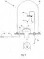
- FIG. 5 is a schematic diagram of a sputtering system 60 similar to the one set forth in U.S. Patent No. 6,586,781 .
- the substrate upon which the sputter layer is intended is indicated at 61 on an electrode (anode) 62 in a chamber 63.
- the pressure in the chamber 63 is typically reduced using a vacuum pump 59 and the desired gas or gases (typically inert or noble gases such as argon) are added to the chamber 63 through the passage 64 and controlled by the valve 65.
- gas molecules become ionized and accelerate to impinge upon (in this case) the silicon target 66 which also serves as the cathode.
- the impinging gas ion will eject silicon ions or atoms 72 which then deposit on the substrate 61 as indicated by the small circles 68.
- the invention is a method of passivating silicon carbide structures and devices and Group III nitride based structures and devices.
- the invention is a method comprising thermally oxidizing a silicon carbide substrate, annealing the thermal oxide in nitrogen oxide (N 2 O), sputter-depositing a non-stoichiometric silicon nitride layer on the oxide layer, and depositing an environmental barrier of stoichiometric silicon nitride (Si 3 N 4 ) by chemical vapor deposition, and in exemplary cases, by plasma enhanced chemical vapor deposition.
- Exemplary annealing techniques are set forth in U.S. Patent No.
- the sputtering is carried out using a silicon target in a substantially hydrogen-free environment, which can incorporate argon (Ar) and nitrogen (N 2 ).
- the method can include sputtering with a pulsed direct current (DC) power source to thereby discharge insulating particles while avoiding arcing.
- DC direct current
- the sputtering can be carried out at room temperature, or at an elevated substrate temperature. If the sputtering is carried out at an elevated substrate temperature, it should be carried out in a manner that avoids exceeding temperatures that would otherwise detrimentally affect the remainder of the device.
- the substrate temperature can be raised to between about 350 °C and 450 °C without detrimental effects.
- the substrate temperature and the gas pressure are typically interrelated and thus are controlled accordingly.
- the method can comprise sputtering in a nitrogen-rich environment to provide a nonstoichiometric silicon nitride.
- the environmental barrier is typically formed of a stoichiometric silicon nitride layer because of its better barrier properties as compared to the nonstoichiometric silicon nitride layer.
- the ion bombardment can be enhanced by applying a radio frequency biased to the substrate, or by lowering the ambient pressure during the sputtering step.
- the method can be carried out in substantially the same manner for Group III nitride based devices, with the exception that a thermal oxide is not included and the silicon nitride is sputtered directly on the Group III nitride device or structure.
- a passivation used on devices consists of first and second passivation.
- the role of the first passivation is to satisfy surface states and lower interface density.
- the role of the second passivation is to encapsulate and protect devices from environmental effects. Both passivations may consist of several different dielectric layers.
- the first passivation consists of two dielectric layers.
- a thermal oxide of 100 to 500 ⁇ is grown at 1200 °C.
- the film growth is followed by a 1200 °C N 2 O anneal for 1 to 5 hours.
- the oxidation and the subsequent anneal lowers interface density.
- a 1000 to 2000 ⁇ SiN layer can be deposited directly on the thermal oxide, following which ohmic contacts and gates are formed.
- ohmic contacts can be formed after oxidation, then sputtered SiN can be deposited, and gates formed.
- about a 1000 ⁇ passivation layer is deposited prior to T top gates to move the gate metal away from the surface and reduce parasitic capacitance.
- the sputtered SiN replaces a more traditionally used PECVD SiN film on top of the thermal oxide layer.
- the sputtered SiN film will contain no hydrogen when a Si target is sputtered in an Ar /N 2 environment.
- a sputtered SiN film can and will eliminate problems associated with hydrogen in the film. It is predicted, although not yet confirmed, that other insulating sputtered nitride films (e.g., aluminum nitride, AlN) can also be used for the same purpose.
- the key to reactively sputtering a nitride film in Ar/N 2 appears to be the use of pulsed DC power source.
- the power source reverses bias polarity periodically (80 to 150 kHz, 1000 to 2000 ns) to discharge insulating particles that build up on the target thus avoiding arcs.
- the SiN passivation can be done at room temperature or at an elevated substrate temperature (350 °C).
- the sputtered SiN film in the first passivation is optimized for minimal device trapping.
- a SiN film index was found to be an important control parameter for device trapping.
- a refractive index of 1.85 to 1.95 was found to be optimum.
- This off-stoichiometry SiN film is deposited in a nitrogen rich environment with minimal bombardment (N 2 flow of 14 to 18 sccm and process pressure of 7 to 10 mT).
- This SiN film although optimum for device passivation, is not a good encapsulant. That problem is addressed in second passivation.
- the second passivation is added after gates and T top are formed.
- the second passivation consists of three dielectric layers.
- the first two dielectric layers are sputtered SiN.
- the first sputtered SiN layer of 1000 to 3000 ⁇ is a nitrogen rich film (N 2 flow of 14 to 18 sccm and process pressure of 7 to 10 mT) with refractive index in the range of 1.85 to 1.95. This film moves the subsequent passivation layers away from the device interface, but does not yet encapsulate.
- the second sputtered SiN layer with thickness of 1000 to 3000 ⁇ is a stoichiometric nitride with refractive index of 2.04 measured at 630 nm.
- This film is deposited at lower nitrogen flow and higher bombardment (N 2 flow of 12 to 14 sccm and process pressure of 1 to 3 mT).
- N 2 flow 12 to 14 sccm and process pressure of 1 to 3 mT.
- the encapsulating properties of this film are improved by ion bombardment, either through lower pressure, or using RF bias on the wafers (about 0.5 W/inch 2 ).
- the sputtered SiN film provides good encapsulation, and also moves the third dielectric layer further away from the device interface.
- the second sputtered SiN layer may not offer adequate step coverage. This is addressed in the third dielectric layer.
- a 2000 to 5000 ⁇ PECVD SiN layer is deposited on top of the sputtered SiN layers using SiH 4 2%, 350 sccm; NH 3 , 4 sccm; N 2 , 200 sccm; He, 90 sccm; pressure, 1 Torr; power, 25 W.
- the critical process parameter in the PECVD SiN deposition is substrate temperature; higher substrate temperatures tend to drive hydrogen out of the film. The substrate temperature is kept as high as other existing films on the wafer allow, typically between about 250 °C to 450 °C.
- the stoichiometric sputtered SiN film offers a barrier to the hydrogen present during PECVD deposition.
- the PECVD offers a final environmental encapsulant with excellent step coverage.
- the first passivation is deposited after T gates are formed.
- the first passivation for GaN devices consists of two layers. A sputtered SiN or AlN is deposited on top surface of the GaN (typically AlGaN). This is followed by a PECVD SiN film.
- the salient feature is again, to move a typical hydrogen contaminated PECVD nitride film away from the device interface and replace it with a sputtered nitride film (SiN or AlN).
- This film can also be an oxynitride of Si or Al.
- a PECVD SiN film is deposited on top of the sputtered passivation layer. The PECVD film offers good step coverage under the gates
- the second passivation of the GaN devices can use sputtered nitrides or PECVD nitrides or the combination of both.
Landscapes
- Formation Of Insulating Films (AREA)
- Junction Field-Effect Transistors (AREA)
Claims (16)
- Passivierte Halbleiterstruktur, die Folgendes umfasst:ein Siliciumcarbidsubstrat (11, 23);eine thermische Oxidationsschicht (12, 27) auf dem Siliciumcarbidsubstrat zum Absenken der Schnittstellendichte zwischen dem Siliciumcarbidsubstrat und der thermischen Oxidationsschicht; undeine passivierte Schicht, die Folgendes umfasst:eine erste gesputterte, nicht-stöchiometrische Siliciumnitridschicht (16, 33) auf der Oxidationsschicht, um parasitäre Kapazität zu reduzieren und Bauelementabfang zu minimieren;eine zweite gesputterte, nicht-stöchiometrische Siliciumnitridschicht (17, 34) auf der ersten Schicht zum Positionieren von nachfolgenden passivierten Schichten weiter von dem Substrat entfernt, ohne die Struktur einzukapseln; undeine gesputterte, stöchiometrische Siliciumnitridschicht (20, 35) auf der zweiten gesputterten Schicht, um die Struktur einzukapseln und die Wasserstoffbarriereeigenschaften der passivierten Schichten zu verstärken; undeine Umweltsperrschicht (14, 36) eines chemisch in der Gasphase abgeschiedenen (CVD) stöchiometrischen Nitrids.
- Passivierte Halbleiterstruktur nach Anspruch 1, wobei die thermische Oxidationsschicht (12, 27) aus Siliciumdioxid mit einer Dicke von 10 bis 50 nm (100 bis 500 A) besteht.
- Passivierte Halbleiterstruktur nach Anspruch 1 oder Anspruch 2, wobei die erste Siliciumnitridschicht (16, 33) 100 bis 200 nm (1000 bis 2000 A) dick ist.
- Passivierte Halbleiterstruktur nach einem der vorhergehenden Ansprüche, wobei die zweite Siliciumnitridschicht (17, 34) 100 bis 300 nm (1000 bis 3000 A) dick ist.
- Passivierte Halbleiterstruktur nach einem der vorhergehenden Ansprüche, wobei die stöchiometrische Verkapselungsschicht (20, 35) 100 bis 300 nm (1000 bis 3000 A) dick ist.
- Passivierte Halbleiterstruktur nach einem der vorhergehenden Ansprüche, wobei die Umweltsperrschicht (14, 36) 200 bis 500 nm (2000 bis 5000 A) dick ist.
- Passivierte Halbleiterstruktur nach einem der vorhergehenden Ansprüche, wobei die Umweltsperrschicht (14, 36) Si3N4 enthält.
- Passivierte Halbleiterstruktur nach einem der vorhergehenden Ansprüche, wobei das Siliciumcarbidsubstrat (11, 23) ein Einkristall mit einem Polytyp, ausgewählt aus den Polytypen 3C, 4H, 6H und 15R von Siliciumcarbid, ist.
- Halbleiterbauelement einschließlich einer passivierten Halbleiterstruktur nach Anspruch 1, wobei:das Siliciumcarbidsubstrat (23) einen ersten Leitfähigkeitstyp aufweist;das Bauelement weiterhin Folgendes umfasst:die jeweiligen Source- und Drainbereiche (24, 25) in dem Substrat, die entgegengesetzte Leitfähigkeitstypen aufweisen und zwischen sich einen Kanal definieren;eine thermische Oxidschicht (27) auf dem Siliciumcarbidsubstrat (23) zwischen dem Sourcebereich und dem Drainbereich; undeinen Gatekontakt (32) auf der thermischen Oxidschicht (27) .
- Halbleiterbauelement nach Anspruch 9, das weiterhin leitende Kontakte (30, 31) in dem Sourcebereich (24) und dem Drainbereich (25) umfasst.
- Verfahren zur Passivierung von Bauelementen mit großem Bandabstand, wobei das Verfahren Folgendes umfasst:Aufbringen einer nicht-stöchiometrischen Nitridschicht ausgewählt aus Siliciumnitrid und Aluminiumnitrid durch Sputtern auf eine Schicht Halbleitermaterial ausgewählt aus Siliciumcarbid und den Nitriden der Gruppe III;Aufbringen einer stöchiometrischen Siliciumnitridschicht auf der nicht-stöchiometrischer Siliciumnitridschicht durch Sputtern und Aufbringen einer Umweltsperrschicht bestehend aus stöchiometrischem Siliciumnitrid durch chemische Dampfabscheidung auf die durch Sputtern aufgebrachte stöchiometrische Schicht.
- Verfahren nach Anspruch 11, welches das Sputtern eines Siliciumtargets in einer im Wesentlichen wasserstofffreien Umgebung umfasst.
- Verfahren nach Anspruch 12, welches das Sputtern des Siliciumtargets in einer aus Argon und Stickstoff bestehenden Umgebung umfasst.
- Verfahren nach Anspruch 13, welches das Sputtern durch eine gepulste Gleichstromquelle umfasst, um dadurch isolierende Teilchen zu entladen und gleichzeitig Lichtbogenbildung zu vermeiden.
- Verfahren nach Anspruch 11, welches das Sputtern bei Raumtemperatur umfasst.
- Verfahren nach Anspruch 11, welches das Sputtern während der Erhöhung der Substrattemperatur umfasst, wobei Temperaturen, welche sich andernfalls schädlich auf das restliche Bauelement auswirken, vermieden werden.
Applications Claiming Priority (2)
| Application Number | Priority Date | Filing Date | Title |
|---|---|---|---|
| US11/169,378 US7525122B2 (en) | 2005-06-29 | 2005-06-29 | Passivation of wide band-gap based semiconductor devices with hydrogen-free sputtered nitrides |
| PCT/US2006/025447 WO2007002860A1 (en) | 2005-06-29 | 2006-06-28 | Passivation of wide band-gap based semiconductor devices with hydrogen-free sputtered nitrides |
Publications (2)
| Publication Number | Publication Date |
|---|---|
| EP1897128A1 EP1897128A1 (de) | 2008-03-12 |
| EP1897128B1 true EP1897128B1 (de) | 2019-11-20 |
Family
ID=36992555
Family Applications (1)
| Application Number | Title | Priority Date | Filing Date |
|---|---|---|---|
| EP06785888.6A Active EP1897128B1 (de) | 2005-06-29 | 2006-06-28 | Passivierung von auf grossem bandabstand basierenden halbleiterbauelementen mit wasserstofffreien gesputterten nitriden |
Country Status (5)
| Country | Link |
|---|---|
| US (2) | US7525122B2 (de) |
| EP (1) | EP1897128B1 (de) |
| JP (1) | JP5028418B2 (de) |
| TW (1) | TWI307919B (de) |
| WO (1) | WO2007002860A1 (de) |
Families Citing this family (29)
| Publication number | Priority date | Publication date | Assignee | Title |
|---|---|---|---|---|
| US7598576B2 (en) * | 2005-06-29 | 2009-10-06 | Cree, Inc. | Environmentally robust passivation structures for high-voltage silicon carbide semiconductor devices |
| US7855401B2 (en) * | 2005-06-29 | 2010-12-21 | Cree, Inc. | Passivation of wide band-gap based semiconductor devices with hydrogen-free sputtered nitrides |
| US7525122B2 (en) * | 2005-06-29 | 2009-04-28 | Cree, Inc. | Passivation of wide band-gap based semiconductor devices with hydrogen-free sputtered nitrides |
| JP4897948B2 (ja) * | 2005-09-02 | 2012-03-14 | 古河電気工業株式会社 | 半導体素子 |
| US20070284614A1 (en) * | 2006-05-24 | 2007-12-13 | Ilesanmi Adesida | Ohmic contacts for semiconductor devices |
| US20080302653A1 (en) * | 2007-03-29 | 2008-12-11 | Applied Materials Inc. | Method And Device For Producing An Anti-Reflection Or Passivation Layer For Solar Cells |
| EP1976022A3 (de) * | 2007-03-29 | 2008-12-03 | Applied Materials, Inc. | Verfahren und Vorrichtung zur Herstellung einer Antireflexionsschicht oder einer Passivierungsschicht für Solarzellen |
| US8703623B2 (en) * | 2009-06-01 | 2014-04-22 | Massachusetts Institute Of Technology | Fabrication technique for gallium nitride substrates |
| KR101731056B1 (ko) * | 2010-08-13 | 2017-04-27 | 서울바이오시스 주식회사 | 오믹 전극 구조체를 갖는 반도체 발광 소자 및 그것을 제조하는 방법 |
| KR102222438B1 (ko) * | 2012-05-10 | 2021-03-04 | 가부시키가이샤 한도오따이 에네루기 켄큐쇼 | 반도체 장치 및 표시 장치 |
| US8937336B2 (en) | 2012-05-17 | 2015-01-20 | The Hong Kong University Of Science And Technology | Passivation of group III-nitride heterojunction devices |
| US8796102B1 (en) * | 2012-08-29 | 2014-08-05 | Crossbar, Inc. | Device structure for a RRAM and method |
| US9991399B2 (en) | 2012-10-04 | 2018-06-05 | Cree, Inc. | Passivation structure for semiconductor devices |
| US8994073B2 (en) * | 2012-10-04 | 2015-03-31 | Cree, Inc. | Hydrogen mitigation schemes in the passivation of advanced devices |
| US9812338B2 (en) * | 2013-03-14 | 2017-11-07 | Cree, Inc. | Encapsulation of advanced devices using novel PECVD and ALD schemes |
| JP2014138111A (ja) * | 2013-01-17 | 2014-07-28 | Fujitsu Ltd | 半導体装置及びその製造方法、電源装置、高周波増幅器 |
| WO2014185034A1 (ja) * | 2013-05-13 | 2014-11-20 | パナソニックIpマネジメント株式会社 | 半導体装置 |
| US9761438B1 (en) * | 2014-05-08 | 2017-09-12 | Hrl Laboratories, Llc | Method for manufacturing a semiconductor structure having a passivated III-nitride layer |
| US9401708B2 (en) | 2014-05-20 | 2016-07-26 | General Electric Company | Gate drive unit and method for controlling a gate drive unit |
| US9824887B2 (en) | 2014-10-14 | 2017-11-21 | Sharp Kabushiki Kaisha | Nitride semiconductor device |
| US10756084B2 (en) * | 2015-03-26 | 2020-08-25 | Wen-Jang Jiang | Group-III nitride semiconductor device and method for fabricating the same |
| WO2016157581A1 (ja) | 2015-03-31 | 2016-10-06 | シャープ株式会社 | 窒化物半導体電界効果トランジスタ |
| JP6300773B2 (ja) * | 2015-10-23 | 2018-03-28 | 三菱電機株式会社 | 半導体圧力センサ |
| JP6773873B2 (ja) * | 2019-11-19 | 2020-10-21 | 株式会社東芝 | 半導体装置 |
| US12598994B2 (en) * | 2021-06-01 | 2026-04-07 | Wolfspeed, Inc. | Multilayer encapsulation for humidity robustness and related fabrication methods |
| US20220384290A1 (en) | 2021-06-01 | 2022-12-01 | Wolfspeed, Inc. | Multilayer encapsulation for humidity robustness and highly accelerated stress tests and related fabrication methods |
| US11842937B2 (en) | 2021-07-30 | 2023-12-12 | Wolfspeed, Inc. | Encapsulation stack for improved humidity performance and related fabrication methods |
| US20230207640A1 (en) * | 2021-12-29 | 2023-06-29 | Nxp Usa, Inc. | Transistor gate structure with insulating layer and method of fabrication therefor |
| US20230317634A1 (en) * | 2022-04-05 | 2023-10-05 | Applied Materials, Inc. | Coatings with diffusion barriers for corrosion and contamination protection |
Citations (1)
| Publication number | Priority date | Publication date | Assignee | Title |
|---|---|---|---|---|
| EP1972013A2 (de) * | 2006-01-10 | 2008-09-24 | Cree, Inc. | Umweltverträgliche passivierungsstrukturen für hochspannungs-siliciumcarbid-halbleiterbauelemente |
Family Cites Families (70)
| Publication number | Priority date | Publication date | Assignee | Title |
|---|---|---|---|---|
| FR2268355B1 (de) * | 1974-04-16 | 1978-01-20 | Thomson Csf | |
| US3895127A (en) | 1974-04-19 | 1975-07-15 | Rca Corp | Method of selectively depositing glass on semiconductor devices |
| US4551353A (en) | 1981-12-30 | 1985-11-05 | Unitrode Corporation | Method for reducing leakage currents in semiconductor devices |
| US4717641A (en) | 1986-01-16 | 1988-01-05 | Motorola Inc. | Method for passivating a semiconductor junction |
| US4799100A (en) | 1987-02-17 | 1989-01-17 | Siliconix Incorporated | Method and apparatus for increasing breakdown of a planar junction |
| US5332697A (en) * | 1989-05-31 | 1994-07-26 | Smith Rosemary L | Formation of silicon nitride by nitridation of porous silicon |
| JPH046835A (ja) * | 1990-04-24 | 1992-01-10 | Sharp Corp | 化合物半導体装置 |
| JPH06291147A (ja) * | 1991-10-22 | 1994-10-18 | American Teleph & Telegr Co <Att> | 集積回路または離散デバイスおよびその製造方法 |
| GB9206086D0 (en) * | 1992-03-20 | 1992-05-06 | Philips Electronics Uk Ltd | Manufacturing electronic devices comprising,e.g.tfts and mims |
| US5612260A (en) | 1992-06-05 | 1997-03-18 | Cree Research, Inc. | Method of obtaining high quality silicon dioxide passivation on silicon carbide and resulting passivated structures |
| US5430324A (en) * | 1992-07-23 | 1995-07-04 | Siliconix, Incorporated | High voltage transistor having edge termination utilizing trench technology |
| SE9500013D0 (sv) | 1995-01-03 | 1995-01-03 | Abb Research Ltd | Semiconductor device having a passivation layer |
| US5972801A (en) * | 1995-11-08 | 1999-10-26 | Cree Research, Inc. | Process for reducing defects in oxide layers on silicon carbide |
| US6316820B1 (en) * | 1997-07-25 | 2001-11-13 | Hughes Electronics Corporation | Passivation layer and process for semiconductor devices |
| US6825501B2 (en) * | 1997-08-29 | 2004-11-30 | Cree, Inc. | Robust Group III light emitting diode for high reliability in standard packaging applications |
| US6303969B1 (en) * | 1998-05-01 | 2001-10-16 | Allen Tan | Schottky diode with dielectric trench |
| TW471049B (en) | 1998-05-22 | 2002-01-01 | United Microelectronics Corp | Metal gate structure and manufacturing method for metal oxide semiconductor |
| US6246076B1 (en) * | 1998-08-28 | 2001-06-12 | Cree, Inc. | Layered dielectric on silicon carbide semiconductor structures |
| US6972436B2 (en) * | 1998-08-28 | 2005-12-06 | Cree, Inc. | High voltage, high temperature capacitor and interconnection structures |
| JP4361625B2 (ja) * | 1998-10-05 | 2009-11-11 | 東京エレクトロン株式会社 | 半導体装置及びその製造方法 |
| US6242784B1 (en) | 1999-06-28 | 2001-06-05 | Intersil Corporation | Edge termination for silicon power devices |
| TW474024B (en) | 1999-08-16 | 2002-01-21 | Cornell Res Foundation Inc | Passivation of GaN based FETs |
| US6373076B1 (en) | 1999-12-07 | 2002-04-16 | Philips Electronics North America Corporation | Passivated silicon carbide devices with low leakage current and method of fabricating |
| US6586781B2 (en) * | 2000-02-04 | 2003-07-01 | Cree Lighting Company | Group III nitride based FETs and HEMTs with reduced trapping and method for producing the same |
| US6939756B1 (en) | 2000-03-24 | 2005-09-06 | Vanderbilt University | Inclusion of nitrogen at the silicon dioxide-silicon carbide interace for passivation of interface defects |
| US6630413B2 (en) | 2000-04-28 | 2003-10-07 | Asm Japan K.K. | CVD syntheses of silicon nitride materials |
| US6686616B1 (en) * | 2000-05-10 | 2004-02-03 | Cree, Inc. | Silicon carbide metal-semiconductor field effect transistors |
| JP2001352056A (ja) * | 2000-06-08 | 2001-12-21 | Fuji Electric Co Ltd | 半導体装置 |
| US6396090B1 (en) * | 2000-09-22 | 2002-05-28 | Industrial Technology Research Institute | Trench MOS device and termination structure |
| US6690042B2 (en) | 2000-09-27 | 2004-02-10 | Sensor Electronic Technology, Inc. | Metal oxide semiconductor heterostructure field effect transistor |
| US6767843B2 (en) * | 2000-10-03 | 2004-07-27 | Cree, Inc. | Method of N2O growth of an oxide layer on a silicon carbide layer |
| US6610366B2 (en) * | 2000-10-03 | 2003-08-26 | Cree, Inc. | Method of N2O annealing an oxide layer on a silicon carbide layer |
| US6573128B1 (en) * | 2000-11-28 | 2003-06-03 | Cree, Inc. | Epitaxial edge termination for silicon carbide Schottky devices and methods of fabricating silicon carbide devices incorporating same |
| JP4011848B2 (ja) | 2000-12-12 | 2007-11-21 | 関西電力株式会社 | 高耐電圧半導体装置 |
| US6528373B2 (en) * | 2001-02-12 | 2003-03-04 | Cree, Inc. | Layered dielectric on silicon carbide semiconductor structures |
| US7141859B2 (en) * | 2001-03-29 | 2006-11-28 | Georgia Tech Research Corporation | Porous gas sensors and method of preparation thereof |
| US6849882B2 (en) | 2001-05-11 | 2005-02-01 | Cree Inc. | Group-III nitride based high electron mobility transistor (HEMT) with barrier/spacer layer |
| US6797586B2 (en) * | 2001-06-28 | 2004-09-28 | Koninklijke Philips Electronics N.V. | Silicon carbide schottky barrier diode and method of making |
| US6740906B2 (en) * | 2001-07-23 | 2004-05-25 | Cree, Inc. | Light emitting diodes including modifications for submount bonding |
| EP2267784B1 (de) | 2001-07-24 | 2020-04-29 | Cree, Inc. | AlGaN/GaN HEMT MIT ISOLIERTEM GATE |
| JP4415531B2 (ja) * | 2002-09-06 | 2010-02-17 | サンケン電気株式会社 | 半導体素子とその製造方法 |
| US20040160118A1 (en) * | 2002-11-08 | 2004-08-19 | Knollenberg Clifford F. | Actuator apparatus and method for improved deflection characteristics |
| US6956239B2 (en) * | 2002-11-26 | 2005-10-18 | Cree, Inc. | Transistors having buried p-type layers beneath the source region |
| US6747338B1 (en) * | 2002-11-27 | 2004-06-08 | Analog Devices, Inc. | Composite dielectric with improved etch selectivity for high voltage MEMS structures |
| US6983653B2 (en) * | 2002-12-13 | 2006-01-10 | Denso Corporation | Flow sensor having thin film portion and method for manufacturing the same |
| US6933544B2 (en) | 2003-01-29 | 2005-08-23 | Kabushiki Kaisha Toshiba | Power semiconductor device |
| WO2005004198A2 (en) * | 2003-06-13 | 2005-01-13 | North Carolina State University | Complex oxides for use in semiconductor devices and related methods |
| JP2005086171A (ja) * | 2003-09-11 | 2005-03-31 | Fujitsu Ltd | 半導体装置及びその製造方法 |
| US7053425B2 (en) | 2003-11-12 | 2006-05-30 | General Electric Company | Gas sensor device |
| DE10358985B3 (de) | 2003-12-16 | 2005-05-19 | Infineon Technologies Ag | Halbleiterbauelement mit einem pn-Übergang und einer auf einer Oberfläche aufgebrachten Passivierungsschicht |
| US7045404B2 (en) * | 2004-01-16 | 2006-05-16 | Cree, Inc. | Nitride-based transistors with a protective layer and a low-damage recess and methods of fabrication thereof |
| DE102004012884B4 (de) | 2004-03-16 | 2011-07-21 | IXYS Semiconductor GmbH, 68623 | Leistungs-Halbleiterbauelement in Planartechnik |
| JP2005286135A (ja) | 2004-03-30 | 2005-10-13 | Eudyna Devices Inc | 半導体装置および半導体装置の製造方法 |
| US7573078B2 (en) | 2004-05-11 | 2009-08-11 | Cree, Inc. | Wide bandgap transistors with multiple field plates |
| US7550783B2 (en) * | 2004-05-11 | 2009-06-23 | Cree, Inc. | Wide bandgap HEMTs with source connected field plates |
| US7332795B2 (en) * | 2004-05-22 | 2008-02-19 | Cree, Inc. | Dielectric passivation for semiconductor devices |
| JP2006032911A (ja) | 2004-06-15 | 2006-02-02 | Ngk Insulators Ltd | 半導体積層構造、半導体素子およびhemt素子 |
| US7221039B2 (en) * | 2004-06-24 | 2007-05-22 | Taiwan Semiconductor Manufacturing Co., Ltd. | Thin film transistor (TFT) device structure employing silicon rich silicon oxide passivation layer |
| US7547928B2 (en) | 2004-06-30 | 2009-06-16 | Interuniversitair Microelektronica Centrum (Imec) | AlGaN/GaN high electron mobility transistor devices |
| US7297995B2 (en) | 2004-08-24 | 2007-11-20 | Micron Technology, Inc. | Transparent metal shielded isolation for image sensors |
| US7345309B2 (en) | 2004-08-31 | 2008-03-18 | Lockheed Martin Corporation | SiC metal semiconductor field-effect transistor |
| US20060118892A1 (en) | 2004-12-02 | 2006-06-08 | Taiwan Semiconductor Manufacturing Company, Ltd. | Methods and Structures to Produce a Strain-Inducing Layer in a Semiconductor Device |
| US20060145190A1 (en) * | 2004-12-31 | 2006-07-06 | Salzman David B | Surface passivation for III-V compound semiconductors |
| SG145706A1 (en) | 2005-02-02 | 2008-09-29 | Agency Science Tech & Res | Method and structure for fabricating iii-v nitride layers on silicon substrates |
| US7525122B2 (en) | 2005-06-29 | 2009-04-28 | Cree, Inc. | Passivation of wide band-gap based semiconductor devices with hydrogen-free sputtered nitrides |
| US7855401B2 (en) | 2005-06-29 | 2010-12-21 | Cree, Inc. | Passivation of wide band-gap based semiconductor devices with hydrogen-free sputtered nitrides |
| US7419892B2 (en) | 2005-12-13 | 2008-09-02 | Cree, Inc. | Semiconductor devices including implanted regions and protective layers and methods of forming the same |
| US7592211B2 (en) | 2006-01-17 | 2009-09-22 | Cree, Inc. | Methods of fabricating transistors including supported gate electrodes |
| US7709269B2 (en) | 2006-01-17 | 2010-05-04 | Cree, Inc. | Methods of fabricating transistors including dielectrically-supported gate electrodes |
| MX2008011844A (es) | 2006-03-13 | 2008-10-02 | Encysive Pharmaceuticals Inc | Formulaciones de sitaxsentano de sodio. |
-
2005
- 2005-06-29 US US11/169,378 patent/US7525122B2/en active Active
-
2006
- 2006-06-28 WO PCT/US2006/025447 patent/WO2007002860A1/en not_active Ceased
- 2006-06-28 EP EP06785888.6A patent/EP1897128B1/de active Active
- 2006-06-28 JP JP2008519580A patent/JP5028418B2/ja active Active
- 2006-06-29 TW TW095123557A patent/TWI307919B/zh active
-
2009
- 2009-03-16 US US12/404,557 patent/US7858460B2/en not_active Expired - Lifetime
Patent Citations (1)
| Publication number | Priority date | Publication date | Assignee | Title |
|---|---|---|---|---|
| EP1972013A2 (de) * | 2006-01-10 | 2008-09-24 | Cree, Inc. | Umweltverträgliche passivierungsstrukturen für hochspannungs-siliciumcarbid-halbleiterbauelemente |
Also Published As
| Publication number | Publication date |
|---|---|
| US20090215280A1 (en) | 2009-08-27 |
| EP1897128A1 (de) | 2008-03-12 |
| US7858460B2 (en) | 2010-12-28 |
| JP2008544578A (ja) | 2008-12-04 |
| JP5028418B2 (ja) | 2012-09-19 |
| TWI307919B (en) | 2009-03-21 |
| TW200707545A (en) | 2007-02-16 |
| US7525122B2 (en) | 2009-04-28 |
| WO2007002860A1 (en) | 2007-01-04 |
| US20070001174A1 (en) | 2007-01-04 |
Similar Documents
| Publication | Publication Date | Title |
|---|---|---|
| US7858460B2 (en) | Passivation of wide band-gap based semiconductor devices with hydrogen-free sputtered nitrides | |
| EP2031648B1 (de) | Passivierung von auf weiten Bandabständen basierten Halbleitervorrichtungen mit wasserstofffrei aufgedampften Nitriden | |
| EP1410444B1 (de) | Isolierendes Gate AlGaN/GaN HEMT | |
| CN1260827C (zh) | 三族氮化物晶体管及其制造方法 | |
| CN103178099A (zh) | Mis型半导体器件及其制造方法 | |
| WO2025052364A1 (en) | Method to tune gate work function in p-gan gate e-mode hemt | |
| CN209487514U (zh) | 一种高质量栅界面的GaN MISFET器件 | |
| CN115472688B (zh) | 一种抗单粒子效应的高电子迁移率晶体管及其制备方法 | |
| US20260040601A1 (en) | Group iii-n device including a hydrogen-blocking layer | |
| US20260033382A1 (en) | Group iii-n device including surface passivation | |
| JP2024148522A (ja) | 窒化物半導体装置および窒化物半導体装置の製造方法 | |
| US20070148879A1 (en) | III-V compound semiconductor heterostructure MOSFET with a high workfunction metal gate electrode and process of making the same | |
| HK1142995A1 (en) | Termination and contact structures for a high voltage gan-based heterojunction transistor | |
| HK1142995B (en) | Termination and contact structures for a high voltage gan-based heterojunction transistor |
Legal Events
| Date | Code | Title | Description |
|---|---|---|---|
| PUAI | Public reference made under article 153(3) epc to a published international application that has entered the european phase |
Free format text: ORIGINAL CODE: 0009012 |
|
| 17P | Request for examination filed |
Effective date: 20080102 |
|
| AK | Designated contracting states |
Kind code of ref document: A1 Designated state(s): AT BE BG CH CY CZ DE DK EE ES FI FR GB GR HU IE IS IT LI LT LU LV MC NL PL PT RO SE SI SK TR |
|
| DAX | Request for extension of the european patent (deleted) | ||
| RIN1 | Information on inventor provided before grant (corrected) |
Inventor name: ALLEN, SCOTT, T. Inventor name: SMITH, RICHARD, PETER Inventor name: MACKENZIE, ANDREW Inventor name: HENNING, JASON, PATRICK Inventor name: RING, ZOLTAN Inventor name: WARD, ALLAN, III Inventor name: SHEPPARD, SCOTT, THOMAS Inventor name: SRIRAM, SAPTHARISHI Inventor name: HAGLEITNER, HELMUT |
|
| 17Q | First examination report despatched |
Effective date: 20080806 |
|
| DAX | Request for extension of the european patent (deleted) | ||
| GRAP | Despatch of communication of intention to grant a patent |
Free format text: ORIGINAL CODE: EPIDOSNIGR1 |
|
| INTG | Intention to grant announced |
Effective date: 20141106 |
|
| APBK | Appeal reference recorded |
Free format text: ORIGINAL CODE: EPIDOSNREFNE |
|
| APBN | Date of receipt of notice of appeal recorded |
Free format text: ORIGINAL CODE: EPIDOSNNOA2E |
|
| APBR | Date of receipt of statement of grounds of appeal recorded |
Free format text: ORIGINAL CODE: EPIDOSNNOA3E |
|
| APAF | Appeal reference modified |
Free format text: ORIGINAL CODE: EPIDOSCREFNE |
|
| INTC | Intention to grant announced (deleted) | ||
| APBT | Appeal procedure closed |
Free format text: ORIGINAL CODE: EPIDOSNNOA9E |
|
| GRAP | Despatch of communication of intention to grant a patent |
Free format text: ORIGINAL CODE: EPIDOSNIGR1 |
|
| STAA | Information on the status of an ep patent application or granted ep patent |
Free format text: STATUS: GRANT OF PATENT IS INTENDED |
|
| RIC1 | Information provided on ipc code assigned before grant |
Ipc: H01L 21/314 20060101AFI20190607BHEP Ipc: H01L 21/318 20060101ALI20190607BHEP Ipc: H01L 29/24 20060101ALI20190607BHEP |
|
| INTG | Intention to grant announced |
Effective date: 20190704 |
|
| GRAS | Grant fee paid |
Free format text: ORIGINAL CODE: EPIDOSNIGR3 |
|
| GRAA | (expected) grant |
Free format text: ORIGINAL CODE: 0009210 |
|
| STAA | Information on the status of an ep patent application or granted ep patent |
Free format text: STATUS: THE PATENT HAS BEEN GRANTED |
|
| AK | Designated contracting states |
Kind code of ref document: B1 Designated state(s): AT BE BG CH CY CZ DE DK EE ES FI FR GB GR HU IE IS IT LI LT LU LV MC NL PL PT RO SE SI SK TR |
|
| REG | Reference to a national code |
Ref country code: GB Ref legal event code: FG4D |
|
| REG | Reference to a national code |
Ref country code: CH Ref legal event code: EP |
|
| REG | Reference to a national code |
Ref country code: IE Ref legal event code: FG4D |
|
| REG | Reference to a national code |
Ref country code: DE Ref legal event code: R096 Ref document number: 602006058845 Country of ref document: DE |
|
| REG | Reference to a national code |
Ref country code: AT Ref legal event code: REF Ref document number: 1205147 Country of ref document: AT Kind code of ref document: T Effective date: 20191215 |
|
| REG | Reference to a national code |
Ref country code: SE Ref legal event code: TRGR |
|
| REG | Reference to a national code |
Ref country code: NL Ref legal event code: MP Effective date: 20191120 |
|
| REG | Reference to a national code |
Ref country code: LT Ref legal event code: MG4D |
|
| PG25 | Lapsed in a contracting state [announced via postgrant information from national office to epo] |
Ref country code: BG Free format text: LAPSE BECAUSE OF FAILURE TO SUBMIT A TRANSLATION OF THE DESCRIPTION OR TO PAY THE FEE WITHIN THE PRESCRIBED TIME-LIMIT Effective date: 20200220 Ref country code: GR Free format text: LAPSE BECAUSE OF FAILURE TO SUBMIT A TRANSLATION OF THE DESCRIPTION OR TO PAY THE FEE WITHIN THE PRESCRIBED TIME-LIMIT Effective date: 20200221 Ref country code: ES Free format text: LAPSE BECAUSE OF FAILURE TO SUBMIT A TRANSLATION OF THE DESCRIPTION OR TO PAY THE FEE WITHIN THE PRESCRIBED TIME-LIMIT Effective date: 20191120 Ref country code: LV Free format text: LAPSE BECAUSE OF FAILURE TO SUBMIT A TRANSLATION OF THE DESCRIPTION OR TO PAY THE FEE WITHIN THE PRESCRIBED TIME-LIMIT Effective date: 20191120 Ref country code: NL Free format text: LAPSE BECAUSE OF FAILURE TO SUBMIT A TRANSLATION OF THE DESCRIPTION OR TO PAY THE FEE WITHIN THE PRESCRIBED TIME-LIMIT Effective date: 20191120 Ref country code: LT Free format text: LAPSE BECAUSE OF FAILURE TO SUBMIT A TRANSLATION OF THE DESCRIPTION OR TO PAY THE FEE WITHIN THE PRESCRIBED TIME-LIMIT Effective date: 20191120 |
|
| PG25 | Lapsed in a contracting state [announced via postgrant information from national office to epo] |
Ref country code: IS Free format text: LAPSE BECAUSE OF FAILURE TO SUBMIT A TRANSLATION OF THE DESCRIPTION OR TO PAY THE FEE WITHIN THE PRESCRIBED TIME-LIMIT Effective date: 20200320 |
|
| PG25 | Lapsed in a contracting state [announced via postgrant information from national office to epo] |
Ref country code: DK Free format text: LAPSE BECAUSE OF FAILURE TO SUBMIT A TRANSLATION OF THE DESCRIPTION OR TO PAY THE FEE WITHIN THE PRESCRIBED TIME-LIMIT Effective date: 20191120 Ref country code: EE Free format text: LAPSE BECAUSE OF FAILURE TO SUBMIT A TRANSLATION OF THE DESCRIPTION OR TO PAY THE FEE WITHIN THE PRESCRIBED TIME-LIMIT Effective date: 20191120 Ref country code: RO Free format text: LAPSE BECAUSE OF FAILURE TO SUBMIT A TRANSLATION OF THE DESCRIPTION OR TO PAY THE FEE WITHIN THE PRESCRIBED TIME-LIMIT Effective date: 20191120 Ref country code: CZ Free format text: LAPSE BECAUSE OF FAILURE TO SUBMIT A TRANSLATION OF THE DESCRIPTION OR TO PAY THE FEE WITHIN THE PRESCRIBED TIME-LIMIT Effective date: 20191120 Ref country code: PT Free format text: LAPSE BECAUSE OF FAILURE TO SUBMIT A TRANSLATION OF THE DESCRIPTION OR TO PAY THE FEE WITHIN THE PRESCRIBED TIME-LIMIT Effective date: 20200412 |
|
| REG | Reference to a national code |
Ref country code: AT Ref legal event code: MK05 Ref document number: 1205147 Country of ref document: AT Kind code of ref document: T Effective date: 20191120 |
|
| REG | Reference to a national code |
Ref country code: DE Ref legal event code: R097 Ref document number: 602006058845 Country of ref document: DE |
|
| PG25 | Lapsed in a contracting state [announced via postgrant information from national office to epo] |
Ref country code: SK Free format text: LAPSE BECAUSE OF FAILURE TO SUBMIT A TRANSLATION OF THE DESCRIPTION OR TO PAY THE FEE WITHIN THE PRESCRIBED TIME-LIMIT Effective date: 20191120 |
|
| PLBE | No opposition filed within time limit |
Free format text: ORIGINAL CODE: 0009261 |
|
| STAA | Information on the status of an ep patent application or granted ep patent |
Free format text: STATUS: NO OPPOSITION FILED WITHIN TIME LIMIT |
|
| 26N | No opposition filed |
Effective date: 20200821 |
|
| PG25 | Lapsed in a contracting state [announced via postgrant information from national office to epo] |
Ref country code: PL Free format text: LAPSE BECAUSE OF FAILURE TO SUBMIT A TRANSLATION OF THE DESCRIPTION OR TO PAY THE FEE WITHIN THE PRESCRIBED TIME-LIMIT Effective date: 20191120 Ref country code: AT Free format text: LAPSE BECAUSE OF FAILURE TO SUBMIT A TRANSLATION OF THE DESCRIPTION OR TO PAY THE FEE WITHIN THE PRESCRIBED TIME-LIMIT Effective date: 20191120 Ref country code: SI Free format text: LAPSE BECAUSE OF FAILURE TO SUBMIT A TRANSLATION OF THE DESCRIPTION OR TO PAY THE FEE WITHIN THE PRESCRIBED TIME-LIMIT Effective date: 20191120 |
|
| PG25 | Lapsed in a contracting state [announced via postgrant information from national office to epo] |
Ref country code: MC Free format text: LAPSE BECAUSE OF FAILURE TO SUBMIT A TRANSLATION OF THE DESCRIPTION OR TO PAY THE FEE WITHIN THE PRESCRIBED TIME-LIMIT Effective date: 20191120 |
|
| REG | Reference to a national code |
Ref country code: CH Ref legal event code: PL |
|
| GBPC | Gb: european patent ceased through non-payment of renewal fee |
Effective date: 20200628 |
|
| PG25 | Lapsed in a contracting state [announced via postgrant information from national office to epo] |
Ref country code: LU Free format text: LAPSE BECAUSE OF NON-PAYMENT OF DUE FEES Effective date: 20200628 |
|
| REG | Reference to a national code |
Ref country code: BE Ref legal event code: MM Effective date: 20200630 |
|
| PG25 | Lapsed in a contracting state [announced via postgrant information from national office to epo] |
Ref country code: GB Free format text: LAPSE BECAUSE OF NON-PAYMENT OF DUE FEES Effective date: 20200628 Ref country code: FR Free format text: LAPSE BECAUSE OF NON-PAYMENT OF DUE FEES Effective date: 20200630 Ref country code: CH Free format text: LAPSE BECAUSE OF NON-PAYMENT OF DUE FEES Effective date: 20200630 Ref country code: IE Free format text: LAPSE BECAUSE OF NON-PAYMENT OF DUE FEES Effective date: 20200628 Ref country code: LI Free format text: LAPSE BECAUSE OF NON-PAYMENT OF DUE FEES Effective date: 20200630 |
|
| PG25 | Lapsed in a contracting state [announced via postgrant information from national office to epo] |
Ref country code: BE Free format text: LAPSE BECAUSE OF NON-PAYMENT OF DUE FEES Effective date: 20200630 |
|
| PG25 | Lapsed in a contracting state [announced via postgrant information from national office to epo] |
Ref country code: TR Free format text: LAPSE BECAUSE OF FAILURE TO SUBMIT A TRANSLATION OF THE DESCRIPTION OR TO PAY THE FEE WITHIN THE PRESCRIBED TIME-LIMIT Effective date: 20191120 Ref country code: CY Free format text: LAPSE BECAUSE OF FAILURE TO SUBMIT A TRANSLATION OF THE DESCRIPTION OR TO PAY THE FEE WITHIN THE PRESCRIBED TIME-LIMIT Effective date: 20191120 |
|
| PGFP | Annual fee paid to national office [announced via postgrant information from national office to epo] |
Ref country code: FI Payment date: 20250625 Year of fee payment: 20 |
|
| PGFP | Annual fee paid to national office [announced via postgrant information from national office to epo] |
Ref country code: DE Payment date: 20250627 Year of fee payment: 20 |
|
| PGFP | Annual fee paid to national office [announced via postgrant information from national office to epo] |
Ref country code: SE Payment date: 20250627 Year of fee payment: 20 |
|
| PGFP | Annual fee paid to national office [announced via postgrant information from national office to epo] |
Ref country code: IT Payment date: 20250619 Year of fee payment: 20 |
|
| REG | Reference to a national code |
Ref country code: DE Ref legal event code: R079 Ref document number: 602006058845 Country of ref document: DE Free format text: PREVIOUS MAIN CLASS: H01L0021314000 Ipc: H10P0014690000 |