EP1890192B1 - Metrology systems and methods for lithography processes - Google Patents
Metrology systems and methods for lithography processes Download PDFInfo
- Publication number
- EP1890192B1 EP1890192B1 EP07113754A EP07113754A EP1890192B1 EP 1890192 B1 EP1890192 B1 EP 1890192B1 EP 07113754 A EP07113754 A EP 07113754A EP 07113754 A EP07113754 A EP 07113754A EP 1890192 B1 EP1890192 B1 EP 1890192B1
- Authority
- EP
- European Patent Office
- Prior art keywords
- test
- corner rounding
- lithography
- corner
- mask
- Prior art date
- Legal status (The legal status is an assumption and is not a legal conclusion. Google has not performed a legal analysis and makes no representation as to the accuracy of the status listed.)
- Ceased
Links
- 238000001459 lithography Methods 0.000 title claims description 199
- 238000000034 method Methods 0.000 title claims description 107
- 238000012360 testing method Methods 0.000 claims description 346
- 239000000463 material Substances 0.000 claims description 119
- 239000004065 semiconductor Substances 0.000 claims description 107
- 238000005259 measurement Methods 0.000 claims description 88
- 239000011358 absorbing material Substances 0.000 claims description 23
- 238000004519 manufacturing process Methods 0.000 claims description 14
- 230000001678 irradiating effect Effects 0.000 claims description 10
- 238000013461 design Methods 0.000 claims description 9
- 238000000059 patterning Methods 0.000 claims description 7
- 238000000206 photolithography Methods 0.000 claims description 6
- 229920002120 photoresistant polymer Polymers 0.000 claims description 4
- 239000011810 insulating material Substances 0.000 claims description 3
- 230000003287 optical effect Effects 0.000 claims description 3
- 238000001015 X-ray lithography Methods 0.000 claims description 2
- 239000004020 conductor Substances 0.000 claims description 2
- 238000012937 correction Methods 0.000 claims description 2
- 238000000609 electron-beam lithography Methods 0.000 claims description 2
- 238000000671 immersion lithography Methods 0.000 claims description 2
- 238000000025 interference lithography Methods 0.000 claims description 2
- 235000012431 wafers Nutrition 0.000 description 15
- VYPSYNLAJGMNEJ-UHFFFAOYSA-N Silicium dioxide Chemical compound O=[Si]=O VYPSYNLAJGMNEJ-UHFFFAOYSA-N 0.000 description 6
- 238000004364 calculation method Methods 0.000 description 3
- 230000000875 corresponding effect Effects 0.000 description 3
- 229910052770 Uranium Inorganic materials 0.000 description 2
- 230000000694 effects Effects 0.000 description 2
- 238000000691 measurement method Methods 0.000 description 2
- 230000001151 other effect Effects 0.000 description 2
- 239000000377 silicon dioxide Substances 0.000 description 2
- 238000012546 transfer Methods 0.000 description 2
- 229910052721 tungsten Inorganic materials 0.000 description 2
- VYZAMTAEIAYCRO-UHFFFAOYSA-N Chromium Chemical compound [Cr] VYZAMTAEIAYCRO-UHFFFAOYSA-N 0.000 description 1
- ZOKXTWBITQBERF-UHFFFAOYSA-N Molybdenum Chemical compound [Mo] ZOKXTWBITQBERF-UHFFFAOYSA-N 0.000 description 1
- 239000006096 absorbing agent Substances 0.000 description 1
- 238000004458 analytical method Methods 0.000 description 1
- 230000005540 biological transmission Effects 0.000 description 1
- 239000003990 capacitor Substances 0.000 description 1
- 230000001413 cellular effect Effects 0.000 description 1
- 229910052804 chromium Inorganic materials 0.000 description 1
- 239000011651 chromium Substances 0.000 description 1
- 229910052681 coesite Inorganic materials 0.000 description 1
- 238000002508 contact lithography Methods 0.000 description 1
- 230000002596 correlated effect Effects 0.000 description 1
- 229910052906 cristobalite Inorganic materials 0.000 description 1
- 230000003247 decreasing effect Effects 0.000 description 1
- 230000001419 dependent effect Effects 0.000 description 1
- 238000000151 deposition Methods 0.000 description 1
- 230000006866 deterioration Effects 0.000 description 1
- 238000005516 engineering process Methods 0.000 description 1
- 238000005530 etching Methods 0.000 description 1
- 238000002513 implantation Methods 0.000 description 1
- 229910052750 molybdenum Inorganic materials 0.000 description 1
- 239000011733 molybdenum Substances 0.000 description 1
- GALOTNBSUVEISR-UHFFFAOYSA-N molybdenum;silicon Chemical compound [Mo]#[Si] GALOTNBSUVEISR-UHFFFAOYSA-N 0.000 description 1
- 229910052710 silicon Inorganic materials 0.000 description 1
- 239000010703 silicon Substances 0.000 description 1
- 235000012239 silicon dioxide Nutrition 0.000 description 1
- 229910052682 stishovite Inorganic materials 0.000 description 1
- 239000000126 substance Substances 0.000 description 1
- 239000000758 substrate Substances 0.000 description 1
- GUVRBAGPIYLISA-UHFFFAOYSA-N tantalum atom Chemical compound [Ta] GUVRBAGPIYLISA-UHFFFAOYSA-N 0.000 description 1
- MZLGASXMSKOWSE-UHFFFAOYSA-N tantalum nitride Chemical compound [Ta]#N MZLGASXMSKOWSE-UHFFFAOYSA-N 0.000 description 1
- 229910001936 tantalum oxide Inorganic materials 0.000 description 1
- 238000010998 test method Methods 0.000 description 1
- 239000010409 thin film Substances 0.000 description 1
- 239000012780 transparent material Substances 0.000 description 1
- 229910052905 tridymite Inorganic materials 0.000 description 1
- 229910052720 vanadium Inorganic materials 0.000 description 1
Images


Classifications
-
- G—PHYSICS
- G03—PHOTOGRAPHY; CINEMATOGRAPHY; ANALOGOUS TECHNIQUES USING WAVES OTHER THAN OPTICAL WAVES; ELECTROGRAPHY; HOLOGRAPHY
- G03F—PHOTOMECHANICAL PRODUCTION OF TEXTURED OR PATTERNED SURFACES, e.g. FOR PRINTING, FOR PROCESSING OF SEMICONDUCTOR DEVICES; MATERIALS THEREFOR; ORIGINALS THEREFOR; APPARATUS SPECIALLY ADAPTED THEREFOR
- G03F7/00—Photomechanical, e.g. photolithographic, production of textured or patterned surfaces, e.g. printing surfaces; Materials therefor, e.g. comprising photoresists; Apparatus specially adapted therefor
- G03F7/70—Microphotolithographic exposure; Apparatus therefor
- G03F7/70425—Imaging strategies, e.g. for increasing throughput or resolution, printing product fields larger than the image field or compensating lithography- or non-lithography errors, e.g. proximity correction, mix-and-match, stitching or double patterning
-
- G—PHYSICS
- G03—PHOTOGRAPHY; CINEMATOGRAPHY; ANALOGOUS TECHNIQUES USING WAVES OTHER THAN OPTICAL WAVES; ELECTROGRAPHY; HOLOGRAPHY
- G03F—PHOTOMECHANICAL PRODUCTION OF TEXTURED OR PATTERNED SURFACES, e.g. FOR PRINTING, FOR PROCESSING OF SEMICONDUCTOR DEVICES; MATERIALS THEREFOR; ORIGINALS THEREFOR; APPARATUS SPECIALLY ADAPTED THEREFOR
- G03F7/00—Photomechanical, e.g. photolithographic, production of textured or patterned surfaces, e.g. printing surfaces; Materials therefor, e.g. comprising photoresists; Apparatus specially adapted therefor
- G03F7/70—Microphotolithographic exposure; Apparatus therefor
- G03F7/70483—Information management; Active and passive control; Testing; Wafer monitoring, e.g. pattern monitoring
Definitions
- the present invention relates generally to a semiconductor device, a lithography mask, a lithography system, methods of making a semiconductor device and algorithms implemented in software or hardware of a lithography system, and more particularly to metrology systems and methods for lithography processes used in the fabrication of semiconductor devices.
- semiconductor devices are used in a variety of electronic applications, such as computers, cellular phones, personal computing devices, and many other applications.
- Semiconductor devices are manufactured by depositing many different types of material layers over a semiconductor workpiece or wafer, and patterning the various material layers using lithography.
- the material layers typically comprise thin films of conductive, semiconductive, and insulating materials that are patterned and etched to form integrated circuits (ICs).
- ICs integrated circuits
- Optical photolithography involves projecting or transmitting light through a pattern made of optically opaque or translucent areas and optically clear or transparent areas on a mask or reticle onto a layer of photosensitive material deposited over a wafer.
- optical lithography techniques such as contact printing, proximity printing, and projection printing have been used to pattern material layers of integrated circuits.
- Lens projection systems and transmission lithography masks are used for patterning, wherein light is passed through the lithography mask to impinge upon a semiconductor wafer or workpiece.
- corner rounding may vary in lithography systems, due to the type of photoresist used, the wavelength of light or energy used in the exposure process, and other parameters of the lithography process, for example.
- Document US 2002/ 0 164 065 A1 which forms the preamble of claims 1,3, 5, 11, 12, 13, 16 and 19, discloses a test mask having a plurality of corner rounding test patterns formed thereon and a semiconductor device having a plurality of corner rounding test features formed thereon, wherein the corner rounding test patterns are contacts of different sizes.
- document US 2002/ 0 164 065A1 discloses a method of making a semiconductor device as well as a corresponding algorithm, wherein the amount of corner rounding of the test features is analyzed for each test feature individually.
- Document US 2006/ 0 093 063 A1 discloses a semiconductor device having at least two L-shaped test features formed thereon. The test features are used for length measurement.
- Document US 4 419 013 A which forms the preamble of claim 21, shows a lithography system and a mask having 1-shaped alignment marks formed thereon improving the alignment accuracy of the lithography system.
- the object of the invention is achieved by the measures of claims 1, 3 and 5, respectively.
- Concerning a first, second and third algorithm the object of the invention is achieved by the measures of claims 11, 12 and 13, respectively.
- Concerning the semiconductor device the object of the invention is achieved by the features of claim 16.
- Concerning the lithography mask the object of the invention is achieved by the features of claim 19 and concerning the lithography system the object of the invention is achieved by the features of claim 21.
- the first, second and third method of making a semiconductor device comprise providing a lithography mask, the lithography mask comprising a substantially opaque or light-absorbing material, a substantially transparent or light-reflecting material coupled to the substantially opaque or light-absorbing material, and a plurality of corner rounding test patterns formed on the substantially opaque or light-absorbing material or the substantially transparent or light-reflecting material.
- a semiconductor wafer is provided having a photosensitive material layer disposed thereon and the photosensitive material layer is irradiated through the lithography mask. A portion of the photosensitive material layer is removed to expose a portion of the wafer, the removed portion based on the corner rounding test patterns of the lithography mask. The exposed portion of the wafer is changed.
- the plurality of corner rounding test patterns comprises a plurality of square test patterns, at least some of the plurality of square test patterns comprising a different size than other of the plurality of square test patterns. Irradiating the photosensitive material layer through the lithography mask and removing the portion of the photosensitive material layer comprise forming a plurality of test features in the photosensitive material layer.
- An amount of corner rounding of the lithography process is determined by analyzing at least one of the test features relative to another one of the test features, wherein determining the amount of corner rounding comprises measuring a first distance from a first corner to a second corner opposite the first corner of a first test feature, measuring a second distance from a first side to a second side opposite the first side of the first test feature, and comparing the second distance and the first distance.
- the plurality of corner rounding test patterns comprises at least one first test pattern having a first angle and at least one second test pattern having a second angle, the first and second test patterns having substantially the same size, an outer corner of the first angle of the first test pattern being proximate yet spaced apart from an outer corner of the second angle of the second test pattern by a first distance on the mask.
- Irradiating the photosensitive material layer through the lithography mask and removing the portion of the photosensitive material layer comprise forming at least two angle-containing features in the photosensitive material layer.
- An amount of corner rounding of the lithography process is determined by analyzing at least one of the angle-containing features relative to another one of the angle-containing features, wherein determining the amount of corner rounding comprises measuring a second distance between an outer corner of a first angle of the first angle-containing feature and an outer corner of a second angle of the second angle-containing feature formed on the layer of photosensitive material of the first semiconductor device.
- the plurality of corner rounding test patterns comprises a plurality of angled test patterns, at least some of the plurality of angled test patterns comprising a different size than other of the plurality of angled test patterns.
- Irradiating the photosensitive material layer through the lithography mask and removing the portion of the photosensitive material layer comprise forming a plurality of angled test features in the photosensitive material layer.
- An amount of corner rounding of the lithography process is determined by analyzing at least one of the angled test features relative to another one of the angled test features by analyzing the shape of the plurality of angled test features to determine whether a portion of each of the plurality of angled test features comprises a straight line.
- the first, second and third algorithms implemented in software or hardware of a lithography system comprise obtaining corner rounding measurement data and calculating an amount of corner rounding of the lithography process by analyzing the corner rounding measurement data.
- obtaining the corner rounding measurement data comprises taking measurements of a first corner rounding test feature relative to at least one second corner rounding test feature of a material layer of a semiconductor device that has been patterned using a mask having a plurality of square corner rounding test patterns formed thereon, wherein at least some of the plurality of square test patterns comprise a different size than other of the plurality of square test patterns, and a lithography process.
- Taking measurement data comprises measuring a first distance from a first corner to a second corner opposite the first corner of the first test feature, measuring a second distance from a first side to a second side opposite the first side of the first test feature, and comparing the second distance and the first distance.
- obtaining the corner rounding measurement data comprises taking measurements of a first angle-containing corner rounding test feature relative to at least one second angle-containing corner rounding test feature of a material layer of a semiconductor device that has been patterned using a mask having a plurality of corner rounding test patterns formed thereon, wherein the plurality of corner rounding test patterns comprise at least one first test pattern having a first angle and at least one second test pattern having a second angle, the first and second test patterns having substantially the same size, an outer corner of the first angle of the first test pattern being proximate yet spaced apart from an outer corner of the second angle of the second test pattern by a first distance on the mask, and a lithography process.
- Taking measurement data comprises measuring a second distance between an outer corner of a first angle of the first angle-containing feature and an outer corner of a second angle of the second angle-containing feature.
- obtaining the corner rounding measurement data comprises taking measurements of a first angled corner rounding test feature relative to at least one second angled corner rounding test feature of a material layer of a semiconductor device that has been patterned using a mask having a plurality of angled corner rounding test patterns formed thereon, at least some of the plurality of angled test patterns comprising a different size than other of the plurality of angled test patterns, and a lithography process.
- Taking measurement data comprises analyzing the shape of the plurality of angled test features to determine whether a portion of each of the plurality of angled test features comprises a straight line.
- the object of the invention is achieved by a semiconductor device comprising a workpiece and a plurality of corner rounding test features disposed in a material layer disposed over the workpiece.
- the plurality of corner rounding test features comprises at least one pair of L-shaped test features being spaced apart from each other, having a first L-shaped test feature comprising two arms that are arranged to each other in a first angle and a second L-shaped test feature comprising two arms that are arranged to each other in a second angle, wherein the amount of the first angle is the same as the amount of the second angle, and wherein an angle bisector of the first angle and an angle bisector of the second angle are disposed along one straight line but extend in opposite directions, the at least one pair of L-shaped test features having substantially the same size.
- a lithography mask comprising a substantially opaque or light-absorbing material, a substantially transparent or light-reflecting material and a plurality of corner rounding test patterns formed on the substantially opaque or light-absorbing material or the substantially transparent or light-reflecting material.
- the plurality of corner rounding test patterns comprise at least one pair of L-shaped test patterns having one first L-shaped test pattern having a first angle and one second L-shaped test pattern having a second angle, wherein the amount of the first angle is the same as the amount of the second angle and wherein an angle bisector of the first angle and an angle bisector of the second angle are disposed along one straight line but extend in opposite directions, an outer corner of the first angle of the first L-shaped test pattern being proximate yet spaced apart from an outer corner of the second angle of the second L-shaped test pattern by a predetermined distance on the test lithography mask and the first and second L-shaped test pattern having substantially the same size.
- a lithography system including a support for a device having a layer of photosensitive material disposed thereon, a projection lens system proximate the support for the device, an illuminator proximate the projection lens system and a lithography mask being disposed between the projection lens system and the illuminator.
- the lithography mask is the lithography mask according to claim 19.
- Figure 1 shows a top view of a prior art semiconductor device that illustrates the problem of corner rounding of features
- Figure 2 shows a top view of a lithography mask in accordance with an embodiment of the present invention, wherein a plurality of corner rounding test patterns comprises squares of different sizes;
- Figure 3 shows a top view of a semiconductor device having a layer of photosensitive material disposed thereon that has been patterned with a plurality of corner rounding test features using the lithography mask shown in Figure 2 ;
- Figure 4 is a flow chart showing a method of determining the amount of corner rounding of a lithography process in accordance with the embodiment of the present invention shown in Figures 2 and 3 ;
- Figure 5 shows a top view of a lithography mask in accordance with an embodiment of the present invention, wherein a plurality of corner rounding test patterns comprises at least two angled test patterns disposed adjacent one another at an outer side of their angles;
- Figure 6 shows a top view of a semiconductor device having a layer of photosensitive material disposed thereon that has been patterned using the lithography mask shown in Figure 5 ;
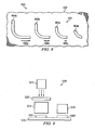
- Figure 7 shows a top view of a lithography mask in accordance with an embodiment of the present invention, wherein a plurality of corner rounding test patterns comprises L shapes of different sizes;
- Figure 8 shows a top view of a semiconductor device having a layer of photosensitive material disposed thereon that has been patterned using the lithography mask shown in Figure 7 ;
- Figure 9 illustrates a lithography system adapted to implement the novel methods of measuring corner rounding in accordance with embodiments of the present invention described herein.
- Figure 1 shows a top view of a prior art semiconductor device 100 that exhibits corner rounding of features 110, e.g., at 112.
- the corner founding 112 may occur due to diffraction, reflection, and other effects that can occur during a lithography process, for example.
- a plurality of features 106 and 110 are formed in a first region 102 and a second region 104, respectively, of the semiconductor device 100, as shown.
- Features 106 in the first region 102 illustrate the desired shape of all features across the surface of the semiconductor device 100.
- the features 106 may comprise rectangular features such as the gates of transistors or other structures, for example.
- the rectangular features 106 include corners 108 where a horizontal side of the rectangular features 106 meets a vertical side, e.g., at a substantially 90° angle, as shown.
- Features 110 in the second region 104 illustrate corner rounding 112 that can occur in lithography processes.
- grounding 112 is evident at the corners of the features 110, rather than 90° angles, as shown at the corners 108 of features 106 in the first region 102.
- corner rounding 112 tends to occur for all features of a particular size and all locations on a semiconductor device 100 of a particular lithography process, for example, rather than occurring in some locations such as in the second region 104 and not in other locations such as in the first region 102 as shown in Figure 1 .
- Corner rounding 112 contributes increasingly to device deterioration as device 100 dimensions are reduced, e.g., as the design node of semiconductor devices 100 shrinks. For example, in 65 nm node technologies, wherein the minimum feature size may be as small as about 55 nm, even moderate corner rounding at a gate contact level or via level can cause devices to be non-functional. As an example, if the features 106 and 110 comprise gates of transistors, the ends of the gates 106 and 110 should extend beyond underlying source and drain regions 114 by predetermined amount, in order to prevent excessive leakage current. Thus, it is important to determine the amount of corner rounding of a particular lithography process, so that dimensions and tolerancing of dimensions of features may be adjusted and tuned accordingly.
- Embodiments of the present invention provide novel methods, test patterns, and test features that may be used to measure corner rounding of lithography processes used to pattern material layers of semiconductor devices.
- a plurality of corner rounding test features are formed on a device using a plurality of angle-containing test patterns on a lithography mask and the plurality of corner rounding test features are analyzed relative to other of the plurality of corner rounding test features to determine the amount of corner rounding.
- the novel measurement techniques and test patterns may be implemented automatically by a SEM tool or other automatic measurement tool. Three.preferred embodiments of the present invention will next be described.
- Figure 2 shows a top view of a lithography mask 220 in accordance with an embodiment of the present invention, wherein a plurality of corner rounding test patterns 222a, 222b, 222c, 222d, and 222e comprises at least two angle-containing patterns.
- the plurality of corner rounding test patterns 222a, 222b, 222c, 222d, and 222e comprises square patterns of different sizes. Angles are located at the corners of each square pattern, and thus the square test patterns 222a, 222b, 222c, 222d, and 222e comprise angle-containing patterns, for example.
- the lithography mask 220 includes a substantially opaque or light-absorbing material 226 and a substantially transparent or light-reflecting material 224 attached or bonded to the substantially opaque or light absorbing material 226.
- material 224 may comprise a substantially opaque or light-absorbing material
- material 226 may comprise a substantially transparent or light-reflecting material, for example, not shown.
- the plurality of corner rounding test patterns 222a, 222b, 222c, 222d, and 222e may comprise patterned squares of the substantially opaque or light-absorbing material 226, e.g., in a bright field binary mask, such as the one shown in Figure 2 .
- the lithography mask 220 may comprise a binary mask, a phase shifting mask, an alternating phase shifting mask, an attenuating phase shifting mask, a bright field mask, a chrome-less mask, a dark field mask, a reflective mask, a transmissive mask, or combinations thereof, as examples.
- the plurality of corner rounding test patterns 222a, 222b, 222c, 222d, and 222e may also comprise apertures or squares formed in the substantially opaque or light-absorbing material 226 and/or in the substantially opaque or light absorbing material 226, for example.
- the test patterns 222a, 222b, 222c, 222d, and 222e each preferably comprise a square having four sides of equal length.
- each adjacent square test pattern 222a, 222b, 222c, 222d, and 222e may comprise sides having a length that is less than a previous adjacent square test pattern 222a, 222b, 222c, 222d, and 222e, as shown.
- the square test patterns 222a, 222b, 222c, 222d, and 222e may comprise sides having lengths that are successively smaller by a predetermined amount, e.g., by about 10 to 50 nm, although alternatively the predetermined amount may comprise other dimensions.
- the square test patterns 222a, 222b, 222c, 222d, and 222e may be positioned relative to one another in other configurations, for example, not shown.
- test pattern 222a comprises sides having a dimension of about 400 nm
- test patterns to the right of test pattern 222a have sides that decrease by about 20 nm from test pattern to test pattern.
- test pattern 222b may comprise sides having a dimension of about 3 80 nm
- test pattern 222c may comprise sides having a dimension of about 360 nm
- test pattern 222d may comprise sides having a dimension of about 340 nm
- test pattern 222e may comprise sides having a dimension of about 320 nm.
- Additional test patterns 222 may be included in 20 nm increments, down to a test pattern having sides of about 100 nm in dimensions, for example, not shown.
- the sides of the square test patterns 222a, 222b, 222e, 222d, and 222e and the incremental difference in size of the sides of the square test patterns 222a, 222b, 222c, 222d, and 222e may comprise different dimensions, for example.
- an amount of corner rounding of a lithography process may be determined by analyzing a plurality of corner rounding test features 236a, 236b, 236c, 236d, and 236e relative to other plurality of corner rounding test features 236a, 236b, 236c, 236d, and 236e formed on a layer of photosensitive material 234 of a semiconductor device 230 using the lithography mask 220 of Figure 2 , for example.
- Figure 3 shows a top view of a semiconductor device 230 having a layer of photosensitive material 234 disposed on a workpiece or substrate 232, wherein the layer of photosensitive material 234 has been patterned using the lithography mask 220 shown in Figure 2 .
- the layer of photosensitive material 234 of the semiconductor device 230 is patterned using a lithography system (e.g., such as the lithography system 570 shown in Figure 9 , to be described further herein), using the lithography mask 220 as a mask.
- a plurality of test features 236a, 236b, 236c, 236d, and 236e are formed in the layer of photosensitive material 234, as shown.
- the plurality of corner rounding test features 236a, 236b, 236c, 236d, and 236e comprises a plurality of substantially square shaped test features 236a, 236b, 236c, and 236d having different sizes and at least one round shaped test feature 236e.
- test features 236a, 236b, 236c, and 236d comprise substantially square test features that exhibit corner rounding.
- the sharp corners of the test patterns 222a, 222b, 222c, and 222d of the mask 220 are rounded during the test pattern transfer, resulted in rounded corners in the test features 236a, 236b, 236c, and 236d formed on the semiconductor device 230 shown in Figure 3 .
- the largest test feature 236e that comprises a circular shape on the semiconductor device 230 indicates the amount of corner rounding of the lithography process.
- the amount of corner rounding is equal to one-half of the length of a side of test pattern 222e of the lithography mask 220 that was used to form the test feature 236e on the semiconductor device 230.
- Smaller test features e.g., continuing to the right of test feature 236e
- the largest test feature 236e comprising a circular shape is the test feature 236e that may be used to determine the amount of corner rounding.
- the amount of corner rounding may be determined manually by an operator of a lithography system, by visually observing the shape of the test features 236a, 236b, 236c, 236d, and 236e formed in the layer of photoresist 234, for example.
- the position of the largest circular shaped test feature 236e may be observed and correlated with the test pattern 222e on the lithography mask 220, to determine the length of a side of the square test pattern 222e, which is then divided by 2 to determine the amount of corner rounding. Because no actual measuring is made of the test features, but rather, the shapes of the test features are visually observed, the tests are low in subjectivity and result in more accurate results.
- Measuring the amount of corner rounding may also be performed by an automatic measurement tool in a preferred embodiment.
- the automatic measurement tool may comprise a SEM, scatterometer, or other automated measurement device adapted to perform measurements of dimensions of test features 236a, 236b, 236c, 236d, and 236e of semiconductor devices 230.
- each side of the test patterns 222a, 222b; 222c, 222d, and 222e preferably have a finite thickness, e.g., about 100 to 200 nm or less, of the opaque or light absorbing material 226 surrounded by the transparent or light reflecting material 224 on the inside and outside of the square test patterns 222a, 222b, 222c, 222d, and 222e (not shown in the Figure 2 ).
- the test features 236a, 236b, 236c, 236d, and 236e of semiconductor devices 230 also comprise square patterns with sides having a finite thickness.
- measurements of the inner radius and/or line-to-line spacing (e.g., from opposing sides of the squares) of the finite thickness-sided square test patterns 236a, 236b, 236c, 236d, and 236e are taken to determine corner rounding, for example.
- Figure 4 is a flow chart 240 showing an exemplary method of determining the amount of corner rounding of a lithography process using an automated measurement tool (e.g., such as automated measurement tool 578 shown in Figure 9 , to be described further herein) in accordance with the embodiment of the present invention shown in Figures 2 and 3 .
- the automatic measuring process is started, e.g., at step 242.
- a test feature 236a e.g., the largest test feature 236a, although the process may be started with any test feature 236a, 236b, 236c, 236d, or 236e
- d 1 and from side-to-side at d 2
- the two measurements d 1 and d 2 are compared, e.g., a calculation of (d 1 -d 2 ) is made at step 246. If (d 1 -d 2 ) is equal to zero (step 248), then the largest circular test pattern 236x has been found, and the automatic measuring process is ended (step 249).
- the amount of corner rounding is 1/2 (d 1 or d 2 ) in this embodiments, for example.
- the result of the calculation (d 1 -d 2 ) may not be exactly zero.
- a predetermined number e.g., a finite number
- the predetermined finite number may comprise about 2 nm, as and example, although other finite numbers may also be used.
- measuring the amount of corner rounding comprises measuring a first distance d 1 from a first corner to a second corner opposite the first corner of a first test feature 236a, measuring a second distance d 2 from a first side to a second side opposite the first side of the first test feature 236a, and comparing the second distance d 2 and the first distance d 1 to determine the amount of corner rounding of the lithography process.
- d 1 is greater than d 2 of a first larger test features 236a
- measurement of at least one second test feature 236b, 236c, 236d, and 236e is then continued, e.g., a third distance (e.g., d 1 ) from a first corner to a second corner opposite the first corner of at least one second test feature 236b is measured, a fourth distance, (e.g., d 2 ,) from a first side to a second side opposite the first side of the at least one second test feature 236b, and the fourth distance d 2 and the third distance d 1 are compared.
- a third distance e.g., d 1
- a fourth distance e.g., d 2
- the measurement of successively smaller additional second test features 236c, 236d, and 236e is continued until one of the first test feature 236a or at least one second test feature 236b, 236c, 236d, or 236e is found wherein the first distance d 1 (e.g., of test feature 236a) is substantially equal to the second distance d 2 (of test feature 236a), or wherein the third distance d 1 (e.g., of a second test feature 236b, 236c, 236d, or 236e) is substantially equal to the fourth distance d 2 (e.g., of a second test feature 236b, 236c, 236d, or 236e).
- the first distance d 1 e.g., of test feature 236a
- the third distance d 1 e.g., of a second test feature 236b, 236c, 236d, or 236e
- the fourth distance d 2 e.g., of a second test feature 236b
- the amount of corner rounding of the lithography process is equal to half of the first distance or second distance, or half of the third distance or fourth distance.
- distance d 2 distance d 1 as test features 236a, 236b, 236c, 236d, or 236e are measured in decreasing size, then the largest test feature 236a, 236b, 236c, 236d, or 236e has been found that comprises a circular shape, for example.
- test features 236a, 236b, 236c, 236d, or 236e are measured according to their size, from larger to smaller, the time taken the determine the amount of corner rounding may be minimized.
- test features 236a, 236b, 236c, 236d, or 236e it is advantageous for the test features 236a, 236b, 236c, 236d, or 236e to be positioned on the semiconductor device 230 in an arrangement that is easily accessible by the automated measurement device, e.g., in rows or columns.
- all of the test features 236a, 236b, 236c, 236d, or 236e may be measured, for example, and the placement of the test features 236a, 236b, 236c, 236d, or 236e may be random, wherein the automated measurement device is adapted to determine using software the location and size of the test patterns of the mask and test features of the semiconductor device.
- corner rounding may be measuring using an inner corner rounding measurement in accordance with an embodiment of the present invention, as shown in Figures 2 through 4 . Corner rounding may also be measuring using an outer corner rounding measurement in accordance with embodiments of the present invention, as shown in Figures 5 and 6 .
- Figure 5 shows a top view of a lithography mask 320 in accordance with another embodiment of the present invention.
- Figure 6 shows a semiconductor device 330 patterned using the lithography mask of Figure 5 .
- the plurality of corner rounding test patterns 350a and 350b comprises at least two angled or angle-containing test patterns disposed adjacent one another at an outer side of their angles.
- the plurality of corner rounding test patterns 350a and 350b comprises at least one first test pattern 350a having a first angle and at least one second test pattern 350b having a second angle, an outer corner 352a of the first angle of a first test pattern 350a being proximate yet spaced apart from an outer corner 352b of the second angle of a second test pattern 350b by a predetermined distance x on the lithography mask 320.
- the corner rounding test patterns 350a and 350b in this embodiment are shown as comprising L shapes; alternatively, the corner rounding test patterns 350a and 350b may also comprise the shape of a square, a rectangle, or letters of the alphabet, or combinations thereof, as examples.
- the angles of the test patterns 350a and 350b are shown as 90 degrees; alternatively, other angles, e.g., greater than 0 and less than 180 degrees, may also be used. Preferably, an angle of 90 degrees or less is used, in some embodiments, for the angles of the test patterns 350a and 350b.
- the test patterns 350a and 350b maybe rotated together such that the line marked "x" between the test patterns is horizontal, vertical, or at many angle, as examples.
- the predetermined distance x between the outer corners 352a and 3 52b of the test patterns 350a and 350b, respectively, may comprise a critical dimension (CD) of a semiconductor device, for example.
- the predetermined distance x may comprise a minimum feature size of a semiconductor device, as another example.
- the predetermined distance x may also comprise other dimensions.
- Figure 6 shows a top view of a semiconductor device 330 comprising a workpiece 332 having a layer of photosensitive material 334 disposed thereon that has been patterned using the lithography mask 320 shown in Figure 5 .
- the test features 354a and 354b comprise substantially L shapes that exhibit corner rounding of the outer corners 352a and 352b of the test patterns 350a and 350b of the lithography mask 320 shown in Figure 5 .
- the corner rounding test features 354a and 354b may comprise other shapes, such as an L, T, Z, U, W, V shape, or other letters of the alphabet, a square, or combinations thereof, for example, depending on the shape of the test patterns 350a and 350b of the mask 320, for example.
- corner rounding is determined using an outer corner rounding measurement, by measuring the distance between outer corners of angled features 354a and 354b.
- the radius of curvature between the outer corners is measured, which can be automated in a SEM tool, for example.
- Figure 7 shows a top view of a lithography mask in accordance with an embodiment of the present invention, wherein a plurality of corner rounding test patterns comprises L shapes of different sizes.
- Figure 8 shows a top view of a semiconductor device having a layer of photosensitive material disposed thereon that has been patterned using the lithography mask shown in Figure 7 .
- This embodiment is similar to the embodiment shown in Figures 2 through 4 , in that successively smaller test patterns 460a, 460b, 460c, and 460d are used to determine the amount of corner rounding.
- the test patterns 460a, 460b, 460c, and 460d are differently shaped, e.g., they comprise L shapes or other angled shapes.
- the test patterns are analyzed relative to one another to determine the amount of corner rounding of the lithography process.
- the lithography mask 430 comprises a plurality of angled or angle-containing test patterns 460a, 460b, 460c, and 460d formed thereon, at least some of the plurality of angled test patterns 460a, 460b, 460c, and 460d comprising a different size than other of the plurality of angled test patterns 460a, 460b, 460c, and 460d.
- Patterning the layer of photosensitive material 434 of the semiconductor device 430 comprises forming a plurality of corner rounded test features 464a, 464b, 464c, and 464d.
- Measuring the amount of corner rounding comprises analyzing the shape of the plurality of angled test features 464a, 464b, 464c, and 464d formed, to determine whether a portion of each of the plurality of angled test features 464a, 464b, 464c, and 464d comprises a straight line.
- the method includes determining which of the plurality of corner rounding features 464a, 464b, 464c, and 464d comprises a largest angled test pattern for which a corner rounded test feature does not comprise a straight line portion 466a, 466b, and 466c, such as test feature 464d in Figure 8 .
- the amount of corner rounding comprises a length of a side of the largest angled test pattern, e.g., test pattern 460d of Figure 7 , for which the corner rounded test feature 464d does not comprise a straight line portion.
- test features 464a, 464b, 464c, and 464d may be observed visually by an operator to determine which test feature 464d is completely curved and has no straight line portion.
- an automated measurement device maybe used to determine the amount of corner rounding, by detecting successively smaller test feature 464a, 464b, 464c, and 464d, stopping the measurements when a test feature 464d having no straight portion is detected, for example.
- the width w of the L-shaped or angled test features 354a, 354b, 464a, 464b, 464c, and/or 464d may comprise a minimum feature size of a lithography system, for example, such as about 100 nm or less, or other dimensions.
- the width of the L-shaped or angled test features 354a, 354b, 464a, 464b, 464c, and/or 464d may comprise other dimensions.
- FIG. 9 illustrates a lithography system 570 adapted to implement the novel methods of measuring corner rounding in accordance with embodiments of the present invention described herein.
- the lithography system 570 includes a support 576 for a device 530 (e.g., such as semiconductor devices 230, 330, and 430 described previously herein) having a layer of photosensitive material disposed thereon.
- the lithography system 570 includes a projection lens system 574 proximate the support 576 for the device 530.
- the projection lens system 574 comprises a plurality of lenses adapted to direct light or energy towards the device 530.
- the lithography system 570 includes an illuminator 572 adapted to produce the light or energy, proximate the projection lens system 574.
- a lithography mask 520 (e.g., such as masks 220, 320, and 420 described previously herein) is disposed between the projection lens system 574 and the illuminator 572.
- the lithography mask 520 includes a plurality of corner rounding test patterns; e.g., square test patterns 222a, 222b, 222c, 222d, and 222e shown in Figure 2 , angled test patterns 350a and 350b shown in Figure 5 , and/or angled test patterns 460a, 460b, 460c, and 460d shown in Figure 7 .
- the lithography mask 520 may comprise a mask designed only for test purposes, e.g., to measure corner rounding and/or other parameters of the lithography system 570 or lithography process.
- the lithography mask 520 may comprise a mask used for patterning a semiconductor device, e.g., active areas are formed on the semiconductor device using the lithography mask 520, and the test features 236a, 236b, 236c, 236d, 236e, 354a, 354b, 464a, 464b, 464c, and/or 464d may be positioned in dedicated test regions of a die.
- corner rounding test features 236a, 236b, 236c, 236d, 236e, 354a, 354b, 464a, 464b, 464c, and/or 464d may be positioned in an unused region of a die or on the kerf of a semiconductor wafer, to save space.
- the corner rounding test features 236a, 236b, 236c, 236d, 236e, 354a, 354b, 464a, 464b, 464c, and/or 464d may be placed in a scribe region of a die, and after corner rounding measurements are made, the corner rounding test features 236a, 236b, 236c, 236d, 236e, 354a, 354b, 464a, 464b, 464c, and/or 464d are destroyed and/or scrapped, e.g., after singulation of the die into individual die, for example.
- the amount of corner rounding of a lithography process performed using the lithography system may be determined by analyzing a plurality of corner rounding test features 236a, 236b, 236c, 236d, 236e, 354a, 354b, 464a, 464b, 464c, and/or 464d formed on the layer of photosensitive material 234, 334, 434, or other material layer of the devices 230, 330, and 430, relative to other of the plurality of corner rounding test features 236a, 236b, 236c; 236d, 236e, 354a, 354b, 464a, 464b, 464c, and/or 464d.
- the amount of corner rounding of the lithography process is determinable by an operator of the lithography system or by an automatic measurement device 578.
- the lithography system 570 may include an automatic measurement device 578, wherein the amount of corner rounding of the lithography process is determinable by the automatic measurement device 578.
- the automatic measurement device 578 may comprise a SEM, a scatterometer, or other automatic measurement tool, as examples.
- the support 576 may be adapted to move the semiconductor device 530 closer to the automatic measurement device 578 for measurements of the corner rounding, as shown at 530', for example.
- the lithography system 570 may comprise an optical lithography system, a non-optical lithography system, an x-ray lithography system, an interference lithography system, a short wavelength lithography system, a Scattering with Angular Limitation in Projection Electron-beam Lithography (SCALPEL) system, an immersion lithography system, a lithography system that utilizes visible, ultraviolet (UV) or extreme UV (EUV) light, or combinations thereof
- SCALPEL Scattering with Angular Limitation in Projection Electron-beam Lithography
- EUV extreme UV
- Embodiments of the present invention may be implemented in lithography systems, steppers, scanners, step-and-scan exposure tools, or other exposure tools, as examples.
- the embodiments described herein are implementable in lithography systems 570 that use both refractive and reflective optics, for example.
- Embodiments of the present invention also include algorithms for measuring and calculating corner rounding of lithography processes, for example.
- An algorithm for calculating corner rounding may be adapted to calculate the corner rounding automatically on the basis of measurement data, for example.
- the algorithm may be implemented in software and/or hardware of the automatic measurement device 578 of the lithography system 570, for example.
- the algorithm may be designed so that the automatic measurement device 578 is adapted to instruct the lithography system 570 to stop further measurements, for example, without requiring operator intervention.
- an algorithm comprises obtaining corner rounding measurement data, wherein obtaining the corner rounding measurement data comprises taking measurements of a first corner rounding test feature relative to at least one second corner rounding test feature of a material layer of a semiconductor device that has been patterned using a mask having a plurality of corner rounding test patterns formed thereon and a lithography process.
- the algorithm includes calculating an amount of corner rounding of the lithography process by analyzing the corner rounding measurement data.
- the calculating step may be automatic, for example.
- the corner rounding measurement data may include indicia of a determination of the amount of corner rounding
- the algorithm may include discontinuing taking measurements of the first corner rounding test feature relative to the at least one second corner rounding test feature, upon indication that the determination of the amount of corner rounding has been achieved, as an example.
- the corner rounding measurements and tests of embodiments of the present invention may be implemented at an initial set-up of a process for a particular semiconductor device design.
- a single wafer or a few wafers may be processed using the lithography system 570 shown in Figure 9 , and lithography process parameters may be changed or altered until an acceptable amount of corner rounding is determined for features of the die.
- the type of photoresist may be changed, the wavelength of energy used, dose of the exposure, and other parameters may be changed to achieved the desired amount of corner rounding.
- the tolerancing (e.g., a tolerance amount) of the semiconductor device design may also be changed, e.g., a mask pattern may be changed, due to the amount of corner rounding measured.
- the layout of a lithography mask may be changed, or an amount of optical proximity correction (OPC) of a lithography mask may be altered, in response to the amount of corner rounding measured, for example.
- OPC optical proximity correction
- the novel corner rounding test and measurement methods may also be implemented periodically, and lithography process parameters may be re-adjusted as needed, for example.
- Embodiments of the present invention include methods of manufacturing semiconductor devices 230, 330, and 430.
- the corner rounding measurements may be made on a first semiconductor device 230, 330, and 430, and a parameter of the lithography process or a design parameter of the mask may be changed or altered, based on the amount of corner rounding determined.
- a second semiconductor device 230, 330, and 430 may then be affected using the altered lithography process or the altered mask.
- a semiconductor wafer with a photosensitive material layer disposed thereon may be provided, and the photosensitive material layer is irradiated through a lithography mask, e.g., such as masks 220, 320, 420, and 520 described herein.
- a lithography mask e.g., such as masks 220, 320, 420, and 520 described herein.
- a portion of the photosensitive material layer is removed to expose a portion of the wafer, the removed portion based on a pattern of the lithography mask.
- the exposed portion of the wafer is then changed.
- the exposed portion may be etched away, altered by exposure to a chemical or implantation process, or a material layer may be formed over the exposed portion, as examples, although other changes may also be implemented to the exposed portion of the wafer.
- a method of manufacturing a semiconductor device includes providing a mask 220, 320, 420, and 520 having a plurality of corner rounding test patterns formed thereon.
- a first semiconductor device is provided, and a layer of photosensitive material of the first semiconductor device is patterned with a plurality of corner rounding test features using the mask and a lithography process.
- An amount of corner rounding of the lithography process is measured by analyzing the plurality of corner rounding test features relative to other of the plurality of corner rounding test features formed on the layer of photosensitive material of the semiconductor device.
- the lithography process or the mask is altered in response to the amount of corner rounding measured, and a second semiconductor device is provided.
- the second semiconductor device is affected using the altered lithography process or the altered mark.
- the second semiconductor device may have a layer of photosensitive material formed thereon, and the layer of photosensitive material may be patterned using the altered lithography process or the altered mask, for example.
- the layer of photosensitive material may then be used to pattern a material layer of a semiconductor device, or change or add a material to the exposed material layer through the patterned layer of photosensitive material, for example.
- Embodiments of the present invention also include semiconductor devices 230, 330, and 430 patterned using the methods and lithography system 570 described herein, for example.
- a semiconductor device 230, 330, and 430 includes a workpiece 232, 332, and 432, and a plurality of corner rounding test features 236a, 236b, 236c, 236d, 236e, 354a, 354b, 464a, 464b, 464c, and/or 464d disposed in a material layer 234, 334, and 434 disposed on the workpiece 232, 332, and 432.
- the material layer may comprise a layer of photosensitive material 234, 334, and 434, as shown in Figures 3 , 6 , and 8 .
- the layer of photosensitive material 234, 334, and 434 may be used as a mask to pattern a material layer (not shown) disposed on the workpiece 232, 332, and 432, for example.
- the material layer may comprise a conductive material, an insulating material, or a semiconductive material, as examples.
- the semiconductor device 230, 330, and 430 may comprise a plurality of die, wherein the plurality of corner rounding test features 236a, 236b, 236c, 236d, 236e, 354a, 354b, 464a, 464b, 464c, and/or 464d are formed in a dedicated region of a die, an unused region of a die, a kerf region of a semiconductor wafer, a test region of a die, a scribe region of a die, or combinations thereof, as example.
- the plurality of corner rounding test features 236a, 236b, 236c, 236d, 236e, 354a, 354b, 464a, 464b, 464c, and/or 464d may comprise an L, T, Z, U, W, or V shape, a square, other shapes, or combinations thereof, as examples.
- the plurality of corner rounding test features may comprise a plurality of substantially square shaped test features 236a, 236b, 236c, 236d having different sizes and at least one round shaped test feature 236e, as shown in Figure 3 .
- the plurality of corner rounding test features may comprise a plurality of substantially L shaped test features 460a, 460b, 460c having different sizes and at least one entirely curved test feature 460d, as shown in Figure 8 .
- the plurality of corner rounding test features may comprise at least two angled test features 350a and 350b disposed adjacent one another at an outer side or outer corner of their angles, as shown in Figure 6 .
- the plurality of corner rounding test features may comprise combinations of all three embodiments on a single die or semiconductor device 230, 330, 430, or 530 for example.
- the results of one or more embodiments of corner rounding measurements may be compared or averaged to determine the corner rounding of a lithography system, for example.
- the masks 220, 320, 420, and 520 described herein may comprise a substantially transparent material such as quartz glass having a thickness of about 1/4", with an opaque material such as chromium, having a thickness of about 30 nm bonded to the quartz glass.
- one of the material layers may comprise about 70 nm of a translucent material such as molybdenum silicon (MoSi), or a bilayer of tantalum and silicon dioxide (Ta/SiO 2 ).
- MoSi molybdenum silicon
- Ti/SiO 2 tantalum and silicon dioxide
- the masks 220, 320, 420, and 520 may also be comprised of multiple layers of silicon and molybdenum to form a reflecting surface and with an absorber material of tantalum nitride (TaN), for example.
- TaN tantalum nitride
- other materials and dimensions may also be used for the material layers of the masks 220, 320, 420, and 520 described herein, for
- Advantages of embodiments of the invention include providing novel methods of determining and measuring corner rounding. Three embodiments are described that enable the measurement of corner rounding of a lithography process automatically using a CD-SEM tool, without requiring any operator intervention.
- the novel measurements and analyses of the corner rounding test features described herein may be implemented in the software or code of a SEM tool, and programmed to perform the measurements and calculations described herein.
- subjectivity and operator error may thus be removed from, corner rounding measurements and tests, providing accurate test results.
- corner rounding test features 236a, 236b, 236c, 236d, 236e, 464a, 464b, 464c, and/or 464d of the embodiments shown in Figures 2, 3 , 7 , and 8 having successively smaller sizes, advantageously, the onset amount of corner rounding of a lithography process can be determined, in embodiments of the present invention, thus reducing the amount of time for the measurements of corner rounding.
- measurements of all of the test features 236a, 236b, 236c, 236d, 236e, 354a, 354b, 464a, 464b, 464c, and/or 464d formed on a device 230, 330, and 430 may be made, and all of the data may be evaluated, for example.
- test patterns 350a and 350b may be required to determine the corner rounding, and only one measurement step is required.
- the distance between the angled test patterns 350a and 350b on the mask 320 may be varied, and a plurality of pairs of test patterns 350a and 350b may be used on a mask 320 to measure the effect of proximity on the corner rounding test features 354a and 354b formed on the semiconductor device 330, for example.
- the novel corner rounding test patterns may be formed in lithography masks dedicated to testing the lithography process of a lithography system, for example.
- the test patterns may be implemented in lithography masks used to manufacture production semiconductor devices, for example.
Landscapes
- Physics & Mathematics (AREA)
- General Physics & Mathematics (AREA)
- Exposure And Positioning Against Photoresist Photosensitive Materials (AREA)
- Preparing Plates And Mask In Photomechanical Process (AREA)
Applications Claiming Priority (1)
| Application Number | Priority Date | Filing Date | Title |
|---|---|---|---|
| US11/504,388 US7794903B2 (en) | 2006-08-15 | 2006-08-15 | Metrology systems and methods for lithography processes |
Publications (2)
| Publication Number | Publication Date |
|---|---|
| EP1890192A1 EP1890192A1 (en) | 2008-02-20 |
| EP1890192B1 true EP1890192B1 (en) | 2012-02-22 |
Family
ID=38668808
Family Applications (1)
| Application Number | Title | Priority Date | Filing Date |
|---|---|---|---|
| EP07113754A Ceased EP1890192B1 (en) | 2006-08-15 | 2007-08-03 | Metrology systems and methods for lithography processes |
Country Status (3)
| Country | Link |
|---|---|
| US (3) | US7794903B2 (enExample) |
| EP (1) | EP1890192B1 (enExample) |
| JP (1) | JP4875568B2 (enExample) |
Families Citing this family (9)
| Publication number | Priority date | Publication date | Assignee | Title |
|---|---|---|---|---|
| JP2013104992A (ja) * | 2011-11-14 | 2013-05-30 | Seiko Epson Corp | 偏光素子、偏光素子の製造方法、プロジェクター、液晶装置、および電子機器 |
| JP6140954B2 (ja) | 2012-09-06 | 2017-06-07 | キヤノン株式会社 | マスクデータ作成方法、それを実行するプログラムおよび情報処理装置 |
| JP6338929B2 (ja) * | 2014-05-23 | 2018-06-06 | 東芝メモリ株式会社 | レチクルマーク配置方法およびレチクルマーク配置プログラム |
| CN104241157B (zh) * | 2014-09-01 | 2017-02-22 | 上海华力微电子有限公司 | 一种对图形结构刻蚀能力的检测方法 |
| KR20170092522A (ko) | 2014-09-08 | 2017-08-11 | 더 리서치 파운데이션 포 더 스테이트 유니버시티 오브 뉴욕 | 금속 격자 및 이의 측정 방법 |
| US10546095B2 (en) | 2017-06-13 | 2020-01-28 | International Business Machines Corporation | Parameter collapsing and corner reduction in an integrated circuit |
| US10274836B2 (en) * | 2017-06-23 | 2019-04-30 | International Business Machines Corporation | Determination of lithography effective dose uniformity |
| CN109634070B (zh) * | 2019-02-01 | 2020-09-01 | 墨研计算科学(南京)有限公司 | 一种基于掩模版拐角圆化的计算光刻方法及装置 |
| WO2021071472A1 (en) * | 2019-10-08 | 2021-04-15 | Applied Materials, Inc. | Universal metrology file, protocol, and process for maskless lithography systems |
Family Cites Families (17)
| Publication number | Priority date | Publication date | Assignee | Title |
|---|---|---|---|---|
| US4419013A (en) | 1981-03-30 | 1983-12-06 | Tre Semiconductor Equipment Corporation | Phase contrast alignment system for a semiconductor manufacturing apparatus |
| JPS5960439A (ja) | 1982-09-30 | 1984-04-06 | Fujitsu Ltd | フオト・マスク |
| JP2995061B2 (ja) | 1988-10-27 | 1999-12-27 | ソニー株式会社 | フォトマスク |
| US5475766A (en) * | 1991-09-05 | 1995-12-12 | Kabushiki Kaisha Toshiba | Pattern inspection apparatus with corner rounding of reference pattern data |
| JPH06138645A (ja) | 1992-10-26 | 1994-05-20 | Fujitsu Ltd | レチクル精度確認パターン,レチクル及びその製造方法 |
| JPH0815854A (ja) | 1994-06-30 | 1996-01-19 | Fujitsu Ltd | 半導体装置の製造方法 |
| JPH08248620A (ja) | 1995-03-15 | 1996-09-27 | Nippon Precision Circuits Kk | レチクルおよびこれを用いたデフォーカスレベル判定方法 |
| JPH09160217A (ja) | 1995-12-08 | 1997-06-20 | Nikon Corp | フォトマスク及びフォトマスクの形成方法 |
| IL123473A (en) * | 1997-02-28 | 2001-08-08 | Fiekowsky Peter J | High accuracy particle dimension measurement system |
| US6368516B1 (en) * | 1999-06-24 | 2002-04-09 | Infineon Technologies North America Corp. | Semiconductor manufacturing methods |
| US6379848B1 (en) | 1999-12-20 | 2002-04-30 | Philips Electronics No. America Corp. | Reticle for use in photolithography and methods for inspecting and making same |
| AU2002245560A1 (en) * | 2001-03-20 | 2002-10-03 | Numerial Technologies, Inc. | System and method of providing mask defect printability analysis |
| US6873720B2 (en) * | 2001-03-20 | 2005-03-29 | Synopsys, Inc. | System and method of providing mask defect printability analysis |
| US6581193B1 (en) * | 2001-06-13 | 2003-06-17 | Kla-Tencor | Apparatus and methods for modeling process effects and imaging effects in scanning electron microscopy |
| US7403572B2 (en) | 2004-11-02 | 2008-07-22 | Topseed Technology Corp. | Method of preventing interferring signal transmission of electronic products |
| JP5044095B2 (ja) | 2004-11-02 | 2012-10-10 | 富士通セミコンダクター株式会社 | 半導体装置の製造方法 |
| EP2093614A1 (en) * | 2008-02-22 | 2009-08-26 | Imec | Split and design guidelines for double patterning |
-
2006
- 2006-08-15 US US11/504,388 patent/US7794903B2/en active Active
-
2007
- 2007-08-03 EP EP07113754A patent/EP1890192B1/en not_active Ceased
- 2007-08-14 JP JP2007211402A patent/JP4875568B2/ja not_active Expired - Fee Related
-
2010
- 2010-07-23 US US12/842,630 patent/US8067135B2/en not_active Expired - Fee Related
-
2011
- 2011-09-27 US US13/246,396 patent/US8394574B2/en not_active Expired - Fee Related
Also Published As
| Publication number | Publication date |
|---|---|
| US8067135B2 (en) | 2011-11-29 |
| EP1890192A1 (en) | 2008-02-20 |
| JP2008096973A (ja) | 2008-04-24 |
| JP4875568B2 (ja) | 2012-02-15 |
| US7794903B2 (en) | 2010-09-14 |
| US20100283052A1 (en) | 2010-11-11 |
| US20120013884A1 (en) | 2012-01-19 |
| US20080044741A1 (en) | 2008-02-21 |
| US8394574B2 (en) | 2013-03-12 |
Similar Documents
| Publication | Publication Date | Title |
|---|---|---|
| EP1890192B1 (en) | Metrology systems and methods for lithography processes | |
| KR100483515B1 (ko) | 광학시스템내의 수차를 검출하는 방법 및 장치 | |
| KR101257961B1 (ko) | 오버레이 측정 타겟 | |
| US7327436B2 (en) | Method for evaluating a local flare, correction method for a mask pattern, manufacturing method for a semiconductor device and a computer program product | |
| US6885429B2 (en) | System and method for automated focus measuring of a lithography tool | |
| KR100549153B1 (ko) | 포토 마스크의 제조 방법 | |
| US7368208B1 (en) | Measuring phase errors on phase shift masks | |
| EP0924758A2 (en) | Method and apparatus for quantifying proximity effect by measuring device performance | |
| US7859645B2 (en) | Masks and methods of manufacture thereof | |
| WO2005041291A2 (en) | Mask and method for using the mask in lithographic processing | |
| JP4157518B2 (ja) | 基板を準備する方法、測定方法、デバイス製造方法、リソグラフィ装置、コンピュータ・プログラム、及び基板 | |
| US7541121B2 (en) | Calibration of optical line shortening measurements | |
| US7279258B2 (en) | Method and arrangement for controlling focus parameters of an exposure tool | |
| WO2018077587A1 (en) | Lithographic apparatus and method | |
| US8198105B2 (en) | Monitor for variation of critical dimensions (CDs) of reticles | |
| US7476473B2 (en) | Process control method, a method for forming monitor marks, a mask for process control, and a semiconductor device manufacturing method | |
| US7498105B2 (en) | Method for checking phase shift angle of phase shift mask, lithography process and phase shift mask | |
| KR20220056726A (ko) | 디포커스 계측방법과 보정방법, 및 그 보정방법을 포함한 반도체 소자 제조방법 | |
| US8723341B2 (en) | Alignment mark and method of manufacturing the same | |
| JP2008192834A (ja) | 露光装置のフレア測定方法と露光装置の管理方法 | |
| KR20070001441A (ko) | 레티클 및 그 제조 방법 | |
| KR20060041456A (ko) | 미스얼라인먼트 검출 마크 |
Legal Events
| Date | Code | Title | Description |
|---|---|---|---|
| PUAI | Public reference made under article 153(3) epc to a published international application that has entered the european phase |
Free format text: ORIGINAL CODE: 0009012 |
|
| AK | Designated contracting states |
Kind code of ref document: A1 Designated state(s): AT BE BG CH CY CZ DE DK EE ES FI FR GB GR HU IE IS IT LI LT LU LV MC MT NL PL PT RO SE SI SK TR |
|
| AX | Request for extension of the european patent |
Extension state: AL BA HR MK YU |
|
| 17P | Request for examination filed |
Effective date: 20080215 |
|
| 17Q | First examination report despatched |
Effective date: 20080401 |
|
| AKX | Designation fees paid |
Designated state(s): DE |
|
| RAP1 | Party data changed (applicant data changed or rights of an application transferred) |
Owner name: INFINEON TECHNOLOGIES AG |
|
| GRAP | Despatch of communication of intention to grant a patent |
Free format text: ORIGINAL CODE: EPIDOSNIGR1 |
|
| GRAS | Grant fee paid |
Free format text: ORIGINAL CODE: EPIDOSNIGR3 |
|
| GRAA | (expected) grant |
Free format text: ORIGINAL CODE: 0009210 |
|
| AK | Designated contracting states |
Kind code of ref document: B1 Designated state(s): DE |
|
| REG | Reference to a national code |
Ref country code: DE Ref legal event code: R096 Ref document number: 602007020809 Country of ref document: DE Effective date: 20120419 |
|
| PLBE | No opposition filed within time limit |
Free format text: ORIGINAL CODE: 0009261 |
|
| STAA | Information on the status of an ep patent application or granted ep patent |
Free format text: STATUS: NO OPPOSITION FILED WITHIN TIME LIMIT |
|
| 26N | No opposition filed |
Effective date: 20121123 |
|
| REG | Reference to a national code |
Ref country code: DE Ref legal event code: R097 Ref document number: 602007020809 Country of ref document: DE Effective date: 20121123 |
|
| PGFP | Annual fee paid to national office [announced via postgrant information from national office to epo] |
Ref country code: DE Payment date: 20221021 Year of fee payment: 16 |
|
| P01 | Opt-out of the competence of the unified patent court (upc) registered |
Effective date: 20230528 |
|
| REG | Reference to a national code |
Ref country code: DE Ref legal event code: R119 Ref document number: 602007020809 Country of ref document: DE |
|
| PG25 | Lapsed in a contracting state [announced via postgrant information from national office to epo] |
Ref country code: DE Free format text: LAPSE BECAUSE OF NON-PAYMENT OF DUE FEES Effective date: 20240301 |