EP1884008B1 - Schutzschalteinrichtung für ein solarmodul - Google Patents
Schutzschalteinrichtung für ein solarmodul Download PDFInfo
- Publication number
- EP1884008B1 EP1884008B1 EP20060753908 EP06753908A EP1884008B1 EP 1884008 B1 EP1884008 B1 EP 1884008B1 EP 20060753908 EP20060753908 EP 20060753908 EP 06753908 A EP06753908 A EP 06753908A EP 1884008 B1 EP1884008 B1 EP 1884008B1
- Authority
- EP
- European Patent Office
- Prior art keywords
- voltage
- circuit
- circuit device
- protective circuit
- mosfet
- Prior art date
- Legal status (The legal status is an assumption and is not a legal conclusion. Google has not performed a legal analysis and makes no representation as to the accuracy of the status listed.)
- Not-in-force
Links
Images


Classifications
-
- H—ELECTRICITY
- H10—SEMICONDUCTOR DEVICES; ELECTRIC SOLID-STATE DEVICES NOT OTHERWISE PROVIDED FOR
- H10F—INORGANIC SEMICONDUCTOR DEVICES SENSITIVE TO INFRARED RADIATION, LIGHT, ELECTROMAGNETIC RADIATION OF SHORTER WAVELENGTH OR CORPUSCULAR RADIATION
- H10F77/00—Constructional details of devices covered by this subclass
- H10F77/95—Circuit arrangements
- H10F77/953—Circuit arrangements for devices having potential barriers
- H10F77/955—Circuit arrangements for devices having potential barriers for photovoltaic devices
-
- H—ELECTRICITY
- H02—GENERATION; CONVERSION OR DISTRIBUTION OF ELECTRIC POWER
- H02H—EMERGENCY PROTECTIVE CIRCUIT ARRANGEMENTS
- H02H3/00—Emergency protective circuit arrangements for automatic disconnection directly responsive to an undesired change from normal electric working condition with or without subsequent reconnection ; integrated protection
- H02H3/02—Details
- H02H3/021—Details concerning the disconnection itself, e.g. at a particular instant, particularly at zero value of current, disconnection in a predetermined order
- H02H3/023—Details concerning the disconnection itself, e.g. at a particular instant, particularly at zero value of current, disconnection in a predetermined order by short-circuiting
-
- Y—GENERAL TAGGING OF NEW TECHNOLOGICAL DEVELOPMENTS; GENERAL TAGGING OF CROSS-SECTIONAL TECHNOLOGIES SPANNING OVER SEVERAL SECTIONS OF THE IPC; TECHNICAL SUBJECTS COVERED BY FORMER USPC CROSS-REFERENCE ART COLLECTIONS [XRACs] AND DIGESTS
- Y02—TECHNOLOGIES OR APPLICATIONS FOR MITIGATION OR ADAPTATION AGAINST CLIMATE CHANGE
- Y02E—REDUCTION OF GREENHOUSE GAS [GHG] EMISSIONS, RELATED TO ENERGY GENERATION, TRANSMISSION OR DISTRIBUTION
- Y02E10/00—Energy generation through renewable energy sources
- Y02E10/50—Photovoltaic [PV] energy
Definitions
- the invention relates to a protective switching device for a solar module, in which a plurality of solar cells is connected in series.
- a protective switching device is off JP 2000 174 308 known.
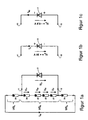
- Solar modules are well known and exist according to Fig. 1a usually from a series circuit of cells, which deliver a single voltage Uz of about 0.5 V to 1 V.
- Uz the voltage on the shaded cells reverses when loaded.
- the permissible reverse voltage of a solar cell is a few V up to a few 10 V.
- the permissible reverse voltage can be exceeded, resulting in local breakdown of the barrier layer and irreversible damage to the solar cell Cell can lead.
- To avoid this unacceptably high reverse voltage is known, ideally a so-called.
- Bypass diode to switch parallel to each cell. This effort is considerable and only in special applications, see eg space travel, portable.
- Fig. 1a Subgroups UG A , UG B , ... UG X formed by series-connected cells, eg 18 to 24, which are each protected by a bypass diode. These are connected via connection points 11, 12 with the respective subgroup. For the sake of clarity, is in FIG. 1a the bypass diode only for the subgroup UG B shown.
- the number of cells combined in a subgroup is selected so that in the worst case the permissible reverse voltage of the disconnected single cell is not exceeded. This results in a typical number of about 18 to 24 cells per subgroup.
- bypass diodes are usually housed in a junction box with the solar panel is exposed, and thus ambient temperatures of about -20 ° C to more than 85 ° C exposed. In one can, typically two or three diodes are accommodated for two or three subgroups UG A , UG B and UG C. To increase the permissible solar generator currents I SG and multiple bypass diodes can be connected in parallel.
- the invention is therefore based on the object to provide a protective switching device for a solar module, which performs the functions of a bypass diode, which provides little power loss and is simple in construction, and ensures a large and long reliability.
- a controllable electrical serving as a bypass element switching element
- the switching path parallel to the plurality of solar cells is connectable and that a supply circuit provides a control voltage for driving the control electrode
- a bypass circuit is provided, which can take over without difficulty the short-circuit or operating point current of the shaded solar cells.
- the controllable bypass element is controlled in its function so that little power loss occurs.
- the isolating circuit which is furthermore provided, the voltage lying in normal operation of the solar cells over the switching path of the switching element can be blocked to the supply circuit, while in the case of shading the isolating circuit switches the voltage lying across the switching path to the supply circuit.
- the supply circuit is designed as a charging circuit for an energy storage or has such that makes a boosting a voltage available in the event of shading in a higher voltage for driving the controllable bypass element.
- the supply voltage of -0.6 V available via the switching path in the event of shading can be used in order to control the controllable bypass element and possibly to supply further circuits.
- controllable bypass element is designed as a MOS field-effect transistor (MOSFET), wherein the inherent in the MOSFET body diode for a short time the solar generator current completely and can be used permanently as a bypass diode for small solar generator currents.
- MOSFET MOS field-effect transistor
- controllable bypass element capacitance in the MOSFET used, the gate capacitance, used as energy storage of the supply circuit or charging circuit, so that no additional memory components are necessary.
- the isolation circuit is designed as an inversely operated bipolar transistor, since it is conventionally operated in collector mode during normal operation and thus can easily block the occurring in normal operation positive drain-source voltage of 20 V.
- the isolation circuit is advantageous to form as a field effect transistor, preferably as a self-conducting J-FET, since this has a low on-resistance, so that the subsequent circuit is almost lossless connected to the voltage of the switching path of the bypass element, the drain-source voltage of the MOSFET.
- the supply circuit and / or charging circuit has a transformer with a positive feedback winding and a first electronic switching element, wherein the switching element and the transformer perform a tilting operation similar to a blocking oscillator, in which the energy stored in the transformer is stored in the energy store, eg the gate capacitance. is transmitted.
- a blocking oscillator in which the energy stored in the transformer is stored in the energy store, eg the gate capacitance. is transmitted.
- the first electronic switching element is inversely connected, so that it simultaneously forms the separation circuit and no additional components for the separation are necessary.
- the first discharge circuit is a non-linear-acting active discharge circuit which is high-impedance above a threshold voltage and below the threshold voltage, wherein the threshold voltage is determined by the required for the complete control of the bypass switching element voltage of its control electrode. As a result, the accumulated power loss within the MOSFET can be further reduced.
- the first discharge circuit with a self-conducting J-FET, which connects the control electrode of the bypass switching element with a reference potential in normal operation and thus prevents accidental switching on of the bypass switching element, and the together in Abschattungsfall forms a timer with a network of diode, capacitor and discharge resistor, which periodically shuts off the bypass switching element after a defined time.
- the control electrode of the bypass switching element in the switched-through state can always remain charged to an optimum value, as a result of which the power loss is further reduced.
- protective switching device has as an essential part of a MOS field effect transistor 1, which is part of a switch unit 30, which will be described later in more detail.
- the drain-source path as a switching path is between the terminals 11 and 12, which are connected to the series connection of the solar cells of the solar module. In normal operation, a positive voltage of 20 V is present at the drain-source path, while in the case of shading a negative drain-source voltage of 0.6 V is present.
- the inherent body diode of the MOSFET 1 is denoted by 2.
- An isolating circuit 40 is connected, on the one hand, to the drain terminal of the MOSFET 1 and, on the other hand, to a supply and / or charging circuit 50 (hereinafter essentially referred to as a charging circuit), the isolating circuit 40, in normal operation, having the positive drain-source voltage of up to approx. 20 V, while in the event of shading it must forward the small negative voltage drop of 0.6 V or less to the subsequent charging circuit 50 with as little loss as possible.
- the charging circuit 50 sets the shadowing case behind the isolation circuit 40 available low negative DC voltage in a required for driving the MOSFET 1 and / or to supply other circuit parts higher positive voltage.
- Concepts based on intermediate storage of energy in a choke coil or transformer and capacitive charge pumps may be used, with a preferred embodiment described later.
- the converted voltage is intermediately stored in an energy store 60, which is drawn here as a capacitor, wherein in a particularly advantageous manner, the gate capacitance of the MOSFET 1 is used directly as energy storage.
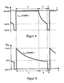
- the gate electrode G of the MOSFET 1 is controlled by a timer circuit 80 time-dependent, wherein the MOSFET is turned on for the most part of the cycle time to reduce the power loss, if necessary operates linearly over a shorter period and is completely blocked over a short period.
- the bypass current of the MOSFET 1 then flows through the body diode 2.
- the protective circuits according to FIGS. 3 . 6 and 7 is according to Fig. 5 in the first two time ranges discharges the gate capacitance of the MOSFET, while it is charged via the charging circuit at the end of the third time range.
- the discharge takes place according to Fig. 9 only in the time ranges 2 and 3, at the end of the fourth time range, the capacity is recharged via the charging circuit.
- a comparator 70 which monitors the drain-source voltage and in the allowable state gives a signal to a logic circuit 90, which also receives the signal of the timer circuit. Monitoring criteria of the comparator circuit 70, for example, the polarity and the height of the drain-source voltage of the MOSFET 1.
- a driver circuit 100 which is like all other circuits connected to the supply or charging circuit 50, controls the gate of the MOSFET 1 depending on the signal Logic circuit.
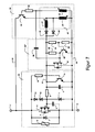
- FIG. 3 a first embodiment of the protective switching device according to the invention is shown with discrete components, wherein partially the function blocks are shown in dashed lines.
- the switch unit 30 has, as already stated, the MOSFET 1 with the body diode 2 and inherently existing gate capacitance 3.
- a first zener diode 7 is connected in the forward direction to the gate terminal by the reference potential line connected to the terminal 12. It serves to limit the gate voltage to a permissible value of, for example, 15 V.
- a transistor 9 is connected with its switching path whose base is connected via a high-resistance resistor 10 to the drain terminal of the MOSFET 1 is.
- a further diode 4 may be connected, which conducts a part of or even the entire bypass current when the MOSFET 1 is not switched on.
- An overvoltage protection element 5, e.g. a varistor or TransZorb diode is connected in parallel with MOSFET 1 and limits extremely high short-time voltage pulses.
- the MOSFET with the body diode 2 inherently present is protected from excessive voltages at the drain-source path and the gate-source path.
- a quick shutdown required and continue to prevent unintentional switching of the MOSFET in normal operation.
- the transistor 9 At a positive drain-source voltage, i. During the transition to normal operation, the transistor 9 is completely controlled by the high-impedance base resistor 10 and discharges the gate capacitance 3 of the MOSFET 1 via the low-impedance resistor 6 very fast (positive feedback). Furthermore, the transistor 9 keeps the gate-source voltage via the series resistor 6 in normal operation to almost 0 V. Thus, an unwanted switching, e.g. reliably prevented by an externally induced gate voltage. The effluent in normal operation on the base resistor 10 leakage current is negligible with appropriate dimensioning.
- MOSFETs are limited to avalanche-resistant, ie if the maximum permissible drain-source voltage, eg greater than 60 V, is temporarily exceeded for a MOSFET specified for 40 V, the MOSFET becomes conductive and limits the voltage peak without being damaged. In this mode of operation, however, the permissible working range can be left and the component can be subject to increased stress. Therefore, the MOSFET is selectively driven via its gate-source path via the zener diode 14 and the diode 13 when an excessive voltage occurs, the gate being raised to a positive potential when the zener voltage of the zener diode 14 is exceeded, and the MOSFET 1 in the linear range is operated. In order to be able to build up a positive gate voltage when the transistor 9 is conductive, the series resistor 6 is required.
- the capacitor is advantageously connected to the side facing away from the gate side of the series resistor 6, since then in the case of a transient overvoltage only the comparatively low gate capacitance 3 via the Zener diode 14 and the diode 13 must be loaded.
- the separation circuit 40 has the task to separate the normal operation positive drain-source voltage of 20 V from the subsequent circuit and the case of Abschattungsfall negative drain-source voltage of 0.6 V with low loss to the subsequent circuit parts forward.
- disconnecting circuit 40 has a normally-on n-channel junction FET (J-FET) 28, whose source is connected to the drain of the MOSFET 1, whose drain is connected to the subsequent supply or charging circuit 50, and whose gate is connected to the reference potential 32 via a high-resistance gate 29.
- This resistor 29 limits the current through the gate diodes at a positive gate-drain or gate-source voltage greater than 0.5 V, as occurs in Abschattungsfall.
- the low-resistance J-FET 28 requires a gate voltage of approximately 5 V, which is negative with respect to both drain and source. This is achieved directly in normal operation for the source-gate path. For the drain-gate path, however, this can only be achieved if the drain potential assumes a positive value. For this purpose, it is necessary that the subsequent supply or charging circuit 50 can receive a blocking voltage in the amount of the threshold voltage of the J-FET, ie about 5 V. This special property is ensured by the charging circuit 50 described below.
- a self-conducting MOSFET can be used, which have a similar behavior, but then a current limiting across the resistor 29 is not necessary, since the gate insulation can typically accommodate ⁇ 20V.
- the supply and / or charging circuit 50 has the task of converting a negative input voltage of 0.6 V into a sufficient for driving the MOSFET 1 positive output voltage of 15 V, for example. Taking into account the decreasing with increasing temperature voltage drop across the body diode 2 of the MOSFET 1 and possibly occurring voltage drops in the isolation circuit 40, a safe start must be ensured even at voltages of even less than 0.4 volts. Furthermore, the charging circuit must be very robust and with minimal effort to create. It additionally takes over the functions of the comparator 70 as well as partially of the time and driver circuits 80, 100 FIG. 2 ,
- the charging circuit 50 has a common-emitter transistor 24 whose emitter is connected to the drain terminal of the J-FET 28 and whose collector is connected to the primary winding 21 of a converter transformer 20.
- the base of the transistor 24 is connected via a series resistor 25 to a positive feedback winding 22.
- In series with the primary winding 21 is an output winding 21 ', whereby the converter transformer 20 is connected as an autotransformer.
- the collector of transistor 24 is connected between primary winding 21 and output winding 21 '.
- the output winding 21 ' is connected via a rectifier diode 23 and the series resistor 6 to the gate capacitance 3 or directly to the additional capacitor 8. Another diode 23 'connects the end of the primary winding to the additional capacitor 8.
- the charging circuit 50 has a transistor 26 whose emitter is connected to the drain terminal of the J-FET 28, whose collector between the diode 3 and the series resistor 6 and its base via a series resistor 27 to the terminal of the positive feedback winding 22.
- a discharge resistor 81 which may be part of a timer circuit 80 ', is connected between the reference potential line 32 and the gate control line 31.
- the MOSFET 1 loaded on eg 15V. If the threshold voltage of the MOSFET 1 is reached at, for example, 5 V gate-source voltage, this goes from fully driven to linear region (region (2)), and the drain-source voltage increases accordingly FIG. 4 slowly. Without the recharging of the gate-source capacitance 3 described below via the charging circuit 50, the MOSFET 1 would go into the completely blocked state, in which case the solar generator current flows completely through the body diode 2, connected to a negative voltage drop of approx 0.4 V up to about 1 V.
- a sufficiently large base current flows in the transistor 24, a significant collector current and thus current through the primary winding 21 of the transformer 20 cause.
- a voltage is induced in the positive feedback winding 22, which adds due to the sense of winding to the voltage between the lines 32 and 34 and thus amplifies the base current, whereby a tilting operation begins.
- the transistor 24 is completely turned on and it builds up according to the inductance of the primary winding 21 and the applied voltage across the primary winding, which substantially corresponds to the voltage applied between the lines 32, 34, a time-increasing primary current.
- the core of the transformer 20 saturates, or if the base current of the transistor 24 is no longer sufficient for complete control, the positive feedback is reversed and the transistor 24 is abruptly blocked.
- the stored energy in the transformer inductance is transmitted through the primary winding 21 and the output winding 21 'and the rectifier diode 23 in the gate capacitance 3 and the additional capacitor 8. This is at the end of the range (3) or at the beginning of the range (1) of the FIGS. 4 and 5 to recognize.
- the MOSFET 1 thus turns on and has, as described, according to its internal resistance only a negative voltage drop of a few millivolts.
- the charging circuit 50 is then not sufficiently powered and is not active.
- the transformer 20 is dimensioned so that the energy stored in it is sufficient to charge the gate capacitance 3 or the capacitor 8 to the desired value of, for example, 15 V already with a converter clock cycle.
- clock always refers to the charging circuit 50
- cycle always refers to the overall circuit.
- the charge cycle consists of two phases: The first phase has been described above and it starts and extends over the duration of the range (3) of the total cycle. The tilting process itself only takes a few ⁇ s, the essential part of the time consists in the "slow” rise of the current to the end of the range (3). Then the second clock phase sets in, in which the energy is transferred from the transformer to the capacitors. This process is on the falling edge, ie partially in the range (3) and in the range (1) of the subsequent cycle. But this reloading process takes a total of only a few ⁇ s.
- the transistor 24 with its base-emitter path assumes not only the switching function but also the function of the comparator 70 FIG. 2 ie it only works if the applied drain-source voltage is high enough.
- the transistor 24 is therefore thermally coupled to the MOSFET 1. Since both components are based on silicon technology, the forward voltages of the body diode and also the base-emitter diode change in the same direction, so that at all temperatures a reliable function of the circuit is ensured.
- the gate capacitance 3 of the MOSFET 1 or the capacitor 8 can not be fully charged, in particular in the case of small solar generator currents.
- the gate of the MOSFET 1 is discharged very quickly via the then turned-on transistor 26 when the tilting process starts, as is apparent FIG. 5 , Area (3) can be seen.
- the MOSFET 1 is momentarily blocking and the drain-source voltage is increasing accordingly Fig. 4 fast from approx. -0.4 V to the threshold value of the tilting process, to approx. -0.6 V, the forward voltage of the body diode 2.
- the transistor 26 thus creates an additional positive feedback.
- the transistor 26 is completely blocked by the then negative voltage at the positive feedback winding 22, so that the gate capacitor 3 and the capacitor 8 can be charged.
- FIGS. 4 and 5 The overall cycle of the circuit after FIG. 3 sits down accordingly FIGS. 4 and 5 from a first, long phase (100 ms) together, in which the MOSFET 1 is completely controlled, a second, shorter phase (20 ms), in which it enters the linear region and the drain-source voltage slowly up to ca -0.4 V and a third, short phase in which it is completely switched off by the positive feedback circuit for a short time (eg 1 ms).
- the accumulating in the second and third phase Quantity of heat is not a problem and can be removed conventionally.
- the drain-source voltage of the MOSFET increases to positive values of approx. 15 V to approx. 20 V.
- both its drain and its source must be positive by about 5 V with respect to the gate, otherwise an unallowable leakage current would flow into the charging circuit 50.
- the emitter bases of the positive voltage transistors 24 and 26 on the line 34 are reverse biased and they can also accept a reverse voltage of up to about 5V, the drain potential of the J-FET 28 may rise to 5V and the J-FET 28 with it, as required, completely lock.
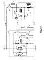
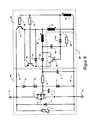
- FIG. 6 is shown a further embodiment, which simplifies the in FIG. 3 shown circuit achieved in that the functions of the separation circuit 40 and the transistor 24 of the supply or charging circuit 50 are summarized. Otherwise, the circuit corresponds to the after FIG. 3 and also the voltage diagrams of Figure 4 and FIG. 5 are applicable.
- the transistor 24 is operated inversely. If, in the case of a bipolar transistor, the emitter and the collector are interchanged, the principal transistor properties are retained; in inverse operation, however, the current amplification decreases by a factor of about 30. This property is met by a correspondingly low-resistance base series resistor 25. In practice, the current limit is sufficient possibly already the ohmic resistance of the positive feedback winding 22, so that no concentrated component 25 must be used.
- the inverse operation of the transistor 24 has the great advantage that it is operated in collector mode during normal operation of the solar module, its base and also the emitter lying DC voltage on the reference potential 32.
- the transistor can easily pick up the 20V voltage that occurs, and it is also possible to use a voltage-proof type of transistor that better resists any overvoltage pulses.
- An oscillation of the supply or charging circuit is excluded because of the negative feedback winding 22 acting as negative feedback in this operating case.
- the transistor 26 continues to be operated conventionally and its function corresponds to that in FIG Fig. 3 , Its emitter, however, is connected to the emitter of the transistor 24.
- the gate of the MOSFET 1 can be discharged quickly via transistor 26, wherein it does not have to absorb negative reverse voltages in this type of interconnection in the Leitendphase of the MOSFET 1 and in normal operation of the module.
- the necessary energy to charge the gate capacitance 3 and the capacitor 8 in a single clock that is transmitted in a single tilting operation of the converter transformer 20 and the transistor 24.
- the charging circuit can also transfer the energy in several cycles, where it charges the gate capacitance of the MOSFET 1 or an energy store in several cycles and then switches off.
- the already mentioned incomplete charging of the gate capacitance or of the capacitor 8 can also be achieved by an appropriate dimensioning, e.g. of the basic series resistor 25, are raised to the principle in order to achieve the permanently linear region of the MOSFET 1.
- the transistor 24 serves as a regulator for the drain-source voltage.
- the MOSFET 1 is not completely controlled in this case, but held over the transistor 24 as a regulator in linear operation.
- a negative voltage of approximately 0.3 V to 0.4 V drops across the drain-source path, which is sufficient to allow the supply or charging circuit 50 to run continuously.
- the losses within the MOSFET 1 are greater than with a fully switched MOSFET.
- the advantage, however, is that no jumps occur in the solar generator voltage or the solar generator current in this linearly operating MOSFET.
- FIG. 7 shows the turn-off instant of the MOSFET 1 from the timer formed by its gate capacitance 3, the optional capacitor 8 and the discharge resistor 81.
- a non-linear active, active gate discharge circuit is used instead of the discharge resistor 81. This has the property that it is high-impedance above a certain threshold voltage, but falls significantly lower impedance when falling below the threshold voltage.
- a circuit with this property can be realized for example by a Schmitt trigger circuit. If the switching point of this trigger circuit, ie the flip-flop of the gate discharge circuit 80 "is set higher than the highest required for complete control of the MOSFET 1 gate voltage, for example to 6 V or greater, so this is after a charge through the Charging circuit 50 initially drop slowly to rapidly fall below the trigger or overturning threshold and trigger a new charging clock With such a circuit, the operation of the MOSFET 1 in the linear range, the in FIG. 4 and FIG. 5 With area (2) is called, avoided and lowered the power loss again.
- a small-signal MOSFET 87 is connected between gate control line 31 and reference potential line 32, whose gate terminal is connected to the collector of a transistor 83 whose emitter is in turn at the reference potential 32.
- the base terminal is connected to a voltage divider 84 85 is connected between gate control line 31 and reference potential line 32.
- a resistor 86 is connected between line 31 and gate terminal of MOSFET 87.
- a capacitor 88 is connected to the positive feedback winding 22.
- the transistor 83 through the voltage divider 84, 85 completely controlled. Its collector potential and thus also the gate potential of the MOSFET 87 are therefore close to the reference potential 32 and the MOSFET 87 is thus blocked.
- the gate capacitance 3 of the MOSFET 1 and the capacitor 8 are slowly discharged via the high-resistance resistors 84, 85 and 86. If the gate voltage from the MOSFET 1 drops below a minimum value, transistor 83 begins to block and the gate voltage of the MOSFET 87 rises. If its threshold voltage is e.g. reaches about 1 ... 2 V in a small-signal MOSFET 87, so its drain-source path is low-resistance and the gate capacitance 3 and the capacitor 8 are discharged quickly. As a result, the base current for the transistor 83 further decreases and it starts a tilting operation.
- FIG. 8 shows a further, particularly advantageous embodiment of the protection circuit. It essentially corresponds to the circuit Fig. 6 , wherein the transistor is omitted together with series resistor 10 and the passive discharge circuit 80 'by an active discharge circuit 80''' has been replaced.
- the core of the active discharge circuit 80 ''' is the normally-on J-FET 81'. It replaces the transistor 9 together with the series resistor 10 by connecting the gate of the MOSFET 1 via the series resistor 6 and the windings 21 'and 21 of the transformer to the reference potential conductor 32 in the normal operation of the solar module.
- unwanted switching of the MOSFET 1 is reliably prevented by externally induced gate voltages or leakage currents of the diodes 13 and 14.
- it allows optimal control of the MOSFET 1 according to Fig. 9 , which leads to a further reduction of the power loss in the bypass switching element.
- the circuit is after Fig. 8 the gate of the MOSFET 1 after the charging process is not discharged by a resistor, but the gate voltage U GS keeps according to Fig. 9 during the entire period 1 its full value. As a result, the MOSFET is very low in this time, and the power loss is correspondingly low.
- the turn-off time of MOSFET 1 is determined by a time constant of the timer formed by capacitor 82 'and resistor 84'.
- the capacitor 82 ' In the charging phase of the capacitors 8 and 3 at the end of the period 4, the capacitor 82 'is also charged via the diode 83' to the sum of the voltages across the three windings 21, 21 'and 22, in FIG If the voltage of the windings 21 and 21 'jumps back to zero after the demagnetization of the transformer 20, the potential at the gate of the J-FET 81' jumps to a value of - 17.5 V. The Thus, J-FET is completely shut off, and ideally no charge can be drained from the capacitors 8 and 3. By the resistor 84 ', the capacitor 82' is discharged slowly, eg within 100 ms.
- Fig. 9 is shown in the time period 2. If this voltage falls below the threshold voltage of the MOSFET 1, it begins to block, and its drain-source voltage U DS increases accordingly Fig. 9 If a value of about - 0.4 V is reached, then as described in the previous circuits, the tilting of the charging circuit 50, connected with a very fast further discharge of the capacitors 8 and 3 by the transistor 26. It follows the section 4, in which the transistor 24 is fully conductive and energy is stored in the transformer 20. At the end of this section, the recharging of the capacitors 8 and 3 and 82 'takes place.
- the described circuits can of course all are constructed with complementary semiconductor types.
- the MOSFET 1 as an additional function can also take over a short circuit of the solar generator voltage during installation, in the event of an inspection or in case of fire.
- the gate terminals of all MOSFETs within a solar generator with a control voltage applied so that the voltage of each individual module is short-circuited.
Landscapes
- Dc-Dc Converters (AREA)
- Charge And Discharge Circuits For Batteries Or The Like (AREA)
- Electronic Switches (AREA)
- Semiconductor Integrated Circuits (AREA)
- Metal-Oxide And Bipolar Metal-Oxide Semiconductor Integrated Circuits (AREA)
- Circuit Arrangement For Electric Light Sources In General (AREA)
- Emergency Protection Circuit Devices (AREA)
- Photovoltaic Devices (AREA)
Priority Applications (1)
| Application Number | Priority Date | Filing Date | Title |
|---|---|---|---|
| EP20110075082 EP2369708A1 (de) | 2005-05-24 | 2006-05-23 | Schutzschalteinrichtung für ein Solarmodul |
Applications Claiming Priority (3)
| Application Number | Priority Date | Filing Date | Title |
|---|---|---|---|
| DE102005024428 | 2005-05-24 | ||
| DE102005036153A DE102005036153B4 (de) | 2005-05-24 | 2005-07-25 | Schutzschalteinrichtung für ein Solarmodul |
| PCT/EP2006/005051 WO2006125664A1 (de) | 2005-05-24 | 2006-05-23 | Schutzschalteinrichtung für ein solarmodul |
Publications (2)
| Publication Number | Publication Date |
|---|---|
| EP1884008A1 EP1884008A1 (de) | 2008-02-06 |
| EP1884008B1 true EP1884008B1 (de) | 2011-05-11 |
Family
ID=36838691
Family Applications (2)
| Application Number | Title | Priority Date | Filing Date |
|---|---|---|---|
| EP20060753908 Not-in-force EP1884008B1 (de) | 2005-05-24 | 2006-05-23 | Schutzschalteinrichtung für ein solarmodul |
| EP20110075082 Withdrawn EP2369708A1 (de) | 2005-05-24 | 2006-05-23 | Schutzschalteinrichtung für ein Solarmodul |
Family Applications After (1)
| Application Number | Title | Priority Date | Filing Date |
|---|---|---|---|
| EP20110075082 Withdrawn EP2369708A1 (de) | 2005-05-24 | 2006-05-23 | Schutzschalteinrichtung für ein Solarmodul |
Country Status (8)
| Country | Link |
|---|---|
| US (1) | US7898114B2 (enExample) |
| EP (2) | EP1884008B1 (enExample) |
| JP (1) | JP4999839B2 (enExample) |
| CN (1) | CN101180781B (enExample) |
| AT (1) | ATE509415T1 (enExample) |
| DE (1) | DE102005036153B4 (enExample) |
| PT (1) | PT1884008E (enExample) |
| WO (1) | WO2006125664A1 (enExample) |
Cited By (2)
| Publication number | Priority date | Publication date | Assignee | Title |
|---|---|---|---|---|
| JP2008546183A (ja) * | 2005-05-24 | 2008-12-18 | フラウンホーファーゲゼルシャフト ツール フォルデルング デル アンゲヴァンテン フォルシユング エー.フアー. | 太陽電池モジュール用の保護回路装置 |
| DE102013106808A1 (de) | 2013-06-28 | 2014-12-31 | Sma Solar Technology Ag | Schaltungsanordnung zur Inline-Spannungsversorgung |
Families Citing this family (122)
| Publication number | Priority date | Publication date | Assignee | Title |
|---|---|---|---|---|
| US11881814B2 (en) | 2005-12-05 | 2024-01-23 | Solaredge Technologies Ltd. | Testing of a photovoltaic panel |
| US10693415B2 (en) | 2007-12-05 | 2020-06-23 | Solaredge Technologies Ltd. | Testing of a photovoltaic panel |
| US8473250B2 (en) | 2006-12-06 | 2013-06-25 | Solaredge, Ltd. | Monitoring of distributed power harvesting systems using DC power sources |
| US8013472B2 (en) | 2006-12-06 | 2011-09-06 | Solaredge, Ltd. | Method for distributed power harvesting using DC power sources |
| US9130401B2 (en) | 2006-12-06 | 2015-09-08 | Solaredge Technologies Ltd. | Distributed power harvesting systems using DC power sources |
| US11309832B2 (en) | 2006-12-06 | 2022-04-19 | Solaredge Technologies Ltd. | Distributed power harvesting systems using DC power sources |
| US11687112B2 (en) | 2006-12-06 | 2023-06-27 | Solaredge Technologies Ltd. | Distributed power harvesting systems using DC power sources |
| US12316274B2 (en) | 2006-12-06 | 2025-05-27 | Solaredge Technologies Ltd. | Pairing of components in a direct current distributed power generation system |
| US11296650B2 (en) | 2006-12-06 | 2022-04-05 | Solaredge Technologies Ltd. | System and method for protection during inverter shutdown in distributed power installations |
| US11855231B2 (en) | 2006-12-06 | 2023-12-26 | Solaredge Technologies Ltd. | Distributed power harvesting systems using DC power sources |
| US9112379B2 (en) | 2006-12-06 | 2015-08-18 | Solaredge Technologies Ltd. | Pairing of components in a direct current distributed power generation system |
| US9088178B2 (en) | 2006-12-06 | 2015-07-21 | Solaredge Technologies Ltd | Distributed power harvesting systems using DC power sources |
| US8816535B2 (en) | 2007-10-10 | 2014-08-26 | Solaredge Technologies, Ltd. | System and method for protection during inverter shutdown in distributed power installations |
| US8319483B2 (en) | 2007-08-06 | 2012-11-27 | Solaredge Technologies Ltd. | Digital average input current control in power converter |
| US11888387B2 (en) | 2006-12-06 | 2024-01-30 | Solaredge Technologies Ltd. | Safety mechanisms, wake up and shutdown methods in distributed power installations |
| US8963369B2 (en) | 2007-12-04 | 2015-02-24 | Solaredge Technologies Ltd. | Distributed power harvesting systems using DC power sources |
| US11569659B2 (en) | 2006-12-06 | 2023-01-31 | Solaredge Technologies Ltd. | Distributed power harvesting systems using DC power sources |
| US8618692B2 (en) | 2007-12-04 | 2013-12-31 | Solaredge Technologies Ltd. | Distributed power system using direct current power sources |
| US8947194B2 (en) | 2009-05-26 | 2015-02-03 | Solaredge Technologies Ltd. | Theft detection and prevention in a power generation system |
| US8319471B2 (en) | 2006-12-06 | 2012-11-27 | Solaredge, Ltd. | Battery power delivery module |
| US11735910B2 (en) | 2006-12-06 | 2023-08-22 | Solaredge Technologies Ltd. | Distributed power system using direct current power sources |
| US8384243B2 (en) | 2007-12-04 | 2013-02-26 | Solaredge Technologies Ltd. | Distributed power harvesting systems using DC power sources |
| WO2008134366A1 (en) * | 2007-04-30 | 2008-11-06 | Bristol, Inc. | Intrinsically safe (is) solar panel |
| CN101933209B (zh) | 2007-12-05 | 2015-10-21 | 太阳能安吉有限公司 | 分布式电力装置中的安全机构、醒来和关闭方法 |
| US8049523B2 (en) | 2007-12-05 | 2011-11-01 | Solaredge Technologies Ltd. | Current sensing on a MOSFET |
| WO2009073867A1 (en) | 2007-12-05 | 2009-06-11 | Solaredge, Ltd. | Parallel connected inverters |
| US9291696B2 (en) | 2007-12-05 | 2016-03-22 | Solaredge Technologies Ltd. | Photovoltaic system power tracking method |
| US11264947B2 (en) | 2007-12-05 | 2022-03-01 | Solaredge Technologies Ltd. | Testing of a photovoltaic panel |
| US20090184746A1 (en) * | 2008-01-22 | 2009-07-23 | Microsemi Corporation | Low Voltage Drop Unidirectional Electronic Valve |
| EP4145691A1 (en) | 2008-03-24 | 2023-03-08 | Solaredge Technologies Ltd. | Switch mode converter including auxiliary commutation circuit for achieving zero current switching |
| EP3121922B1 (en) | 2008-05-05 | 2020-03-04 | Solaredge Technologies Ltd. | Direct current power combiner |
| IT1390778B1 (it) * | 2008-07-01 | 2011-09-23 | St Microelectronics Srl | Architettura per diodo di by-pass di celle in serie di un pannello fotovoltaico |
| SG160241A1 (en) * | 2008-09-15 | 2010-04-29 | Alternative Energy Technology | Photovoltaic cell circuit |
| DE102008052037B3 (de) * | 2008-10-16 | 2010-04-08 | Moeller Gmbh | Solarmodul |
| CN102217087A (zh) * | 2008-11-17 | 2011-10-12 | 应用材料股份有限公司 | 用于背接触太阳能电池及模块的集成旁路二极管组件 |
| US8050804B2 (en) * | 2008-12-15 | 2011-11-01 | Array Converter, Inc. | Detection and prevention of hot spots in a solar panel |
| US20100186795A1 (en) | 2009-01-28 | 2010-07-29 | Stephen Joseph Gaul | Connection systems and methods for solar cells |
| EP2430663A1 (en) * | 2009-05-12 | 2012-03-21 | Ramot at Tel-Aviv University Ltd. | System and method for controlling a group of photovoltaic generators |
| EP2427915B1 (en) | 2009-05-22 | 2013-09-11 | Solaredge Technologies Ltd. | Electrically isolated heat dissipating junction box |
| US8169252B2 (en) * | 2009-07-09 | 2012-05-01 | Microsemi Corporation | Low voltage drop closed loop unidirectional electronic valve |
| EP3035392A1 (de) | 2009-08-26 | 2016-06-22 | Fraunhofer-Gesellschaft zur Förderung der angewandten Forschung e.V. | Bypass- und schutzschaltung für ein solarmodul und verfahren zum steuern eines solarmoduls |
| US8482156B2 (en) | 2009-09-09 | 2013-07-09 | Array Power, Inc. | Three phase power generation from a plurality of direct current sources |
| DE102009042084A1 (de) * | 2009-09-18 | 2011-06-22 | Gehrlicher Solar AG, 85609 | Wartungsarmes elektronisches Bauelement zur Verhinderung von Rückströmen bei gleichzeitigem Schutz vor Überströmen in Photovoltaikanlagen |
| US8263920B2 (en) * | 2009-09-30 | 2012-09-11 | The Boeing Company | Diodeless terrestrial photovoltaic solar power array |
| US9324885B2 (en) | 2009-10-02 | 2016-04-26 | Tigo Energy, Inc. | Systems and methods to provide enhanced diode bypass paths |
| FR2951886B1 (fr) | 2009-10-23 | 2016-02-05 | Commissariat Energie Atomique | Commande avec ralentissement de l'ouverture d'un interrupteur electronique |
| US12418177B2 (en) | 2009-10-24 | 2025-09-16 | Solaredge Technologies Ltd. | Distributed power system using direct current power sources |
| KR101025795B1 (ko) * | 2009-12-30 | 2011-04-04 | 안현구 | 전하 릴레이 인핸서 및 인핸서를 구비한 태양전지 시스템 |
| FR2955209B1 (fr) * | 2010-01-12 | 2015-06-05 | Arnaud Thierry | Systeme de gestion et de commande de panneaux photovoltaiques |
| JP4985795B2 (ja) * | 2010-01-29 | 2012-07-25 | サンケン電気株式会社 | 太陽光発電装置及び太陽光発電システム |
| DE102010007495A1 (de) * | 2010-02-09 | 2011-08-11 | Wieland Electric GmbH, 96052 | Modulbypassschaltung für ein Photovoltaikmodul |
| US9425783B2 (en) * | 2010-03-15 | 2016-08-23 | Tigo Energy, Inc. | Systems and methods to provide enhanced diode bypass paths |
| IT1400922B1 (it) * | 2010-05-14 | 2013-07-02 | St Microelectronics Srl | Diodo di by-pass o interruttore per sorgente dc realizzato con un mosfet a bassa resistenza di conduzione e relativo circuito di controllo autoalimentato con mezzi di disabilitazione della sorgente dc in caso di incendio o altro rischio |
| IT1400921B1 (it) * | 2010-05-14 | 2013-07-02 | St Microelectronics Srl | Diodo di by-pass o interruttore realizzato con un mosfet a bassa resistenza di conduzione e relativo circuito di controllo autoalimentato |
| DE102010023549B4 (de) * | 2010-06-03 | 2016-03-24 | Dmos Gmbh | Photovoltaikgenerator mit Schaltungsanlage und Verfahren zum Schutz von Photovoltaikmodulen |
| US8665575B2 (en) | 2010-06-25 | 2014-03-04 | International Business Machines Corporation | Solar module with overheat protection |
| DE102010036816A1 (de) * | 2010-08-03 | 2012-02-09 | Newtos Ag | Verfahren und Vorrichtung zur Überwachung und Steuerung einer Photovoltaik-Anlage |
| TWI437601B (zh) * | 2010-10-08 | 2014-05-11 | Nexpower Technology Corp | 具複合金屬層保護斷路器之太陽能模組 |
| GB2485527B (en) | 2010-11-09 | 2012-12-19 | Solaredge Technologies Ltd | Arc detection and prevention in a power generation system |
| US10673229B2 (en) | 2010-11-09 | 2020-06-02 | Solaredge Technologies Ltd. | Arc detection and prevention in a power generation system |
| US10673222B2 (en) | 2010-11-09 | 2020-06-02 | Solaredge Technologies Ltd. | Arc detection and prevention in a power generation system |
| US10230310B2 (en) | 2016-04-05 | 2019-03-12 | Solaredge Technologies Ltd | Safety switch for photovoltaic systems |
| DE102010052009A1 (de) | 2010-11-19 | 2012-05-24 | Kostal Industrie Elektrik Gmbh | Photovoltaikanlage und Photovoltaikmodul |
| DE102010053500A1 (de) | 2010-11-23 | 2012-05-24 | Trimos Gmbh | Photovoltaikgenerator mit Schutzschaltungsanlage für Photovoltaikmodule |
| GB2486408A (en) | 2010-12-09 | 2012-06-20 | Solaredge Technologies Ltd | Disconnection of a string carrying direct current |
| GB2483317B (en) | 2011-01-12 | 2012-08-22 | Solaredge Technologies Ltd | Serially connected inverters |
| JP5626798B2 (ja) * | 2011-02-04 | 2014-11-19 | シャープ株式会社 | 太陽光発電システム、スイッチングシステム、およびバイパス装置 |
| US9716196B2 (en) * | 2011-02-09 | 2017-07-25 | Alta Devices, Inc. | Self-bypass diode function for gallium arsenide photovoltaic devices |
| CN102130630B (zh) * | 2011-03-10 | 2013-02-20 | 苏州盖娅智能科技有限公司 | 太阳模组的并联保护电路 |
| DE102012010083B4 (de) | 2011-05-23 | 2023-04-27 | Microsemi Corp. | Photovoltaische Sicherheitsabschaltungsvorrichtung |
| EP2528097A1 (en) | 2011-05-27 | 2012-11-28 | Nederlandse Organisatie voor toegepast -natuurwetenschappelijk onderzoek TNO | Photovoltaic device and method of manufacturing the same |
| JP2012254008A (ja) * | 2011-05-31 | 2012-12-20 | Sensata Technologies Inc | 電力発生器モジュールの接続性制御 |
| DE102011107297A1 (de) * | 2011-07-15 | 2013-01-17 | Kostal Industrie Elektrik Gmbh | Photovoltaikmodul und Photovoltaikanlage |
| DE102011082160A1 (de) * | 2011-09-06 | 2013-03-07 | Robert Bosch Gmbh | Schutzschalteinrichtung, Photovoltaikanlage und Verfahren zum Betrieb einer solchen |
| US8570005B2 (en) | 2011-09-12 | 2013-10-29 | Solaredge Technologies Ltd. | Direct current link circuit |
| US9112430B2 (en) | 2011-11-03 | 2015-08-18 | Firelake Acquisition Corp. | Direct current to alternating current conversion utilizing intermediate phase modulation |
| US8630077B2 (en) * | 2011-12-22 | 2014-01-14 | Sunpower Corporation | Circuits and methods for limiting open circuit voltage of photovoltaic strings |
| GB2498365A (en) * | 2012-01-11 | 2013-07-17 | Solaredge Technologies Ltd | Photovoltaic module |
| GB2498791A (en) | 2012-01-30 | 2013-07-31 | Solaredge Technologies Ltd | Photovoltaic panel circuitry |
| US9853565B2 (en) | 2012-01-30 | 2017-12-26 | Solaredge Technologies Ltd. | Maximized power in a photovoltaic distributed power system |
| GB2498790A (en) | 2012-01-30 | 2013-07-31 | Solaredge Technologies Ltd | Maximising power in a photovoltaic distributed power system |
| GB2499991A (en) | 2012-03-05 | 2013-09-11 | Solaredge Technologies Ltd | DC link circuit for photovoltaic array |
| US8901603B2 (en) | 2012-03-29 | 2014-12-02 | Steven Andrew Robbins | Surge protection circuit for power MOSFETs used as active bypass diodes in photovoltaic solar power systems |
| EP2651035B1 (en) | 2012-04-11 | 2017-05-03 | Imec | Low voltage drop unidirectional smart bypass elements |
| US10115841B2 (en) | 2012-06-04 | 2018-10-30 | Solaredge Technologies Ltd. | Integrated photovoltaic panel circuitry |
| CN102916056B (zh) * | 2012-09-25 | 2015-09-23 | 谢可勋 | 太阳能电池组件保护电路、太阳能接线盒及太阳能发电系统 |
| CN102916393B (zh) * | 2012-10-09 | 2014-11-26 | 祝厉华 | 太阳能电池保护器、太阳能电池组及太阳能电池保护芯片 |
| US9941813B2 (en) | 2013-03-14 | 2018-04-10 | Solaredge Technologies Ltd. | High frequency multi-level inverter |
| US9548619B2 (en) | 2013-03-14 | 2017-01-17 | Solaredge Technologies Ltd. | Method and apparatus for storing and depleting energy |
| EP3506370B1 (en) | 2013-03-15 | 2023-12-20 | Solaredge Technologies Ltd. | Bypass mechanism |
| US9178353B2 (en) | 2013-03-27 | 2015-11-03 | Sunfield Semiconductor, Inc. | Active bypass diode circuit and solar power module with arc flash mitigation feature |
| CN104218929A (zh) * | 2013-05-30 | 2014-12-17 | 快捷半导体(苏州)有限公司 | 真正的逆向电流阻断电路、方法、负载开关及便携式设备 |
| JP6201182B2 (ja) * | 2013-10-09 | 2017-09-27 | 国立研究開発法人宇宙航空研究開発機構 | 昇降圧コンバータを多段接続した太陽電池部分影補償装置 |
| CN103560160B (zh) * | 2013-11-06 | 2016-03-23 | 无锡清莲新能源科技有限公司 | 太阳电池组件 |
| US9318974B2 (en) | 2014-03-26 | 2016-04-19 | Solaredge Technologies Ltd. | Multi-level inverter with flying capacitor topology |
| CN103972864B (zh) * | 2014-05-15 | 2017-03-15 | 电子科技大学 | 一种用于太阳能电池的旁路电路 |
| CN104009713A (zh) * | 2014-05-26 | 2014-08-27 | 扬州虹扬科技发展有限公司 | 一种自动识别光伏电池板组件热斑效应的电路装置 |
| TWI562392B (en) * | 2014-08-15 | 2016-12-11 | Eosmem Corp | Low voltage drop unidirectional electronic valve and solar panel using the same |
| CN104916737B (zh) * | 2014-12-09 | 2016-11-02 | 重庆平伟实业股份有限公司 | 一种光伏旁路模块的封装工艺 |
| US9496710B2 (en) * | 2014-12-29 | 2016-11-15 | Solarcity Corporation | Rapid shutdown solid state circuit for photovoltaic energy generation systems |
| DE102015103247A1 (de) * | 2015-03-05 | 2016-09-08 | Ge Energy Power Conversion Technology Limited | Schaltmodul mit Kurzschlussschutz und Leistungselektronikmodul mit diesem |
| EP3113232A1 (de) * | 2015-06-30 | 2017-01-04 | Anton Naebauer | Optimiertes photovoltaik modul mit bypass-netzwerk |
| JP6543133B2 (ja) * | 2015-08-19 | 2019-07-10 | 株式会社東芝 | 電力供給装置及びその制御方法 |
| DE102016102417B4 (de) * | 2016-02-11 | 2023-12-21 | Sma Solar Technology Ag | Schutzschaltung für ein Photovoltaik (PV)-Modul, Verfahren zum Betrieb der Schutzschaltung und Photovoltaik (PV)-Anlage mit einer derartigen Schutzschaltung |
| CN117130027A (zh) | 2016-03-03 | 2023-11-28 | 太阳能安吉科技有限公司 | 用于映射发电设施的方法 |
| US10599113B2 (en) | 2016-03-03 | 2020-03-24 | Solaredge Technologies Ltd. | Apparatus and method for determining an order of power devices in power generation systems |
| US11081608B2 (en) | 2016-03-03 | 2021-08-03 | Solaredge Technologies Ltd. | Apparatus and method for determining an order of power devices in power generation systems |
| US11018623B2 (en) | 2016-04-05 | 2021-05-25 | Solaredge Technologies Ltd. | Safety switch for photovoltaic systems |
| US11177663B2 (en) | 2016-04-05 | 2021-11-16 | Solaredge Technologies Ltd. | Chain of power devices |
| US12057807B2 (en) | 2016-04-05 | 2024-08-06 | Solaredge Technologies Ltd. | Chain of power devices |
| KR101898587B1 (ko) | 2016-05-04 | 2018-09-13 | 엘지전자 주식회사 | 태양광 모듈, 및 이를 구비하는 태양광 시스템 |
| DE102016213944A1 (de) * | 2016-07-28 | 2018-02-01 | Ellenberger & Poensgen Gmbh | Verfahren und Vorrichtung zur Ansteuerung eines Halbleiterschalters |
| US12395068B2 (en) | 2017-03-29 | 2025-08-19 | Solaredge Technologies Ltd. | Bypass circuit and method to bypass power modules in power system |
| DE102016117229B4 (de) | 2016-09-13 | 2018-12-06 | Sma Solar Technology Ag | Solarmodul und Energieerzeugungsanlage |
| CN106656033A (zh) * | 2016-10-27 | 2017-05-10 | 上海电机学院 | 光伏晶体板在线故障监控方法 |
| US11495414B2 (en) * | 2020-06-26 | 2022-11-08 | Taka Solar Corporation | Solar cell systems and methods of making the same |
| CN108695843B (zh) * | 2017-03-29 | 2023-09-22 | 太阳能安吉科技有限公司 | 旁路电路和在电力系统中旁通电力模块的方法 |
| CN107749742A (zh) * | 2017-11-17 | 2018-03-02 | 无锡工赢智能科技有限公司 | 一种太阳能旁路二极管模块 |
| CN108111121A (zh) * | 2017-12-14 | 2018-06-01 | 常州星海电子股份有限公司 | 一种光伏旁路二极管 |
| WO2020219995A1 (en) * | 2019-04-25 | 2020-10-29 | Aerovironment | System and method for solar cell array diagnostics in high altitude long endurance aircraft |
| DE102019008062A1 (de) * | 2019-11-20 | 2021-05-20 | JOKER Tech GmbH | Solarmodul mit langen Solarzellensträngen |
| US11500367B2 (en) * | 2020-09-23 | 2022-11-15 | Rockwell Automation Technologies, Inc. | Display for self-powered industrial automation component |
Family Cites Families (17)
| Publication number | Priority date | Publication date | Assignee | Title |
|---|---|---|---|---|
| DE3307202A1 (de) * | 1983-03-01 | 1984-09-06 | Siemens AG, 1000 Berlin und 8000 München | Solarzellenmodul |
| US4718185A (en) * | 1986-11-07 | 1988-01-12 | Solar Signage, Inc. | Modular solar generating system |
| DE10331780B4 (de) | 2003-07-11 | 2005-06-09 | Günther Spelsberg GmbH & Co. KG | Elektrische Anschluß- und Verbindungsdose |
| US5131341A (en) * | 1990-12-03 | 1992-07-21 | Edwin Newman | Solar powered electric ship system |
| JPH09102622A (ja) | 1995-10-03 | 1997-04-15 | Nissin Electric Co Ltd | 太陽光発電システムの太陽電池モジュールの故障検出装置 |
| JP2000059986A (ja) * | 1998-04-08 | 2000-02-25 | Canon Inc | 太陽電池モジュ―ルの故障検出方法および装置ならびに太陽電池モジュ―ル |
| JP2000174308A (ja) * | 1998-12-01 | 2000-06-23 | Toshiba Corp | 太陽電池発電モジュール |
| DE19916742C1 (de) * | 1999-04-13 | 2000-08-24 | Angew Solarenergie Ase Gmbh | Schaltungsanordnung zur Stromerzeugung mit Solarzellen |
| JP2001068706A (ja) * | 1999-08-25 | 2001-03-16 | Sanyo Electric Co Ltd | 太陽電池装置 |
| FR2807882B1 (fr) * | 2000-04-18 | 2002-05-24 | Centre Nat Rech Scient | Dispositif anti-points chauds pour module photovoltaique et module photovoltaique equipe d'un tel dispositif |
| JP2002010520A (ja) * | 2000-06-15 | 2002-01-11 | Casio Comput Co Ltd | 太陽電池回路 |
| US6635817B2 (en) * | 2001-12-06 | 2003-10-21 | Koninklijke Philips Electronics N.V. | Solar cell array having lattice or matrix structure and method of arranging solar cells and panels |
| JP4111734B2 (ja) * | 2002-03-27 | 2008-07-02 | シャープ株式会社 | 太陽電池モジュール |
| DE10222621A1 (de) * | 2002-05-17 | 2003-11-27 | Josef Steger | Verfahren und Schaltungsanordnung zur Steuer- und Regelung von Photovoltaikanlagen |
| US7190531B2 (en) * | 2003-06-03 | 2007-03-13 | Rensselaer Polytechnic Institute | Concentrating type solar collection and daylighting system within glazed building envelopes |
| JP4080408B2 (ja) * | 2003-10-07 | 2008-04-23 | 松下電器産業株式会社 | 電池用保護icおよびそれを利用した電池パック |
| DE102005036153B4 (de) * | 2005-05-24 | 2007-03-22 | Fraunhofer-Gesellschaft zur Förderung der angewandten Forschung e.V. | Schutzschalteinrichtung für ein Solarmodul |
-
2005
- 2005-07-25 DE DE102005036153A patent/DE102005036153B4/de not_active Expired - Fee Related
-
2006
- 2006-05-23 EP EP20060753908 patent/EP1884008B1/de not_active Not-in-force
- 2006-05-23 EP EP20110075082 patent/EP2369708A1/de not_active Withdrawn
- 2006-05-23 JP JP2008512777A patent/JP4999839B2/ja not_active Expired - Fee Related
- 2006-05-23 US US11/914,679 patent/US7898114B2/en active Active
- 2006-05-23 PT PT06753908T patent/PT1884008E/pt unknown
- 2006-05-23 AT AT06753908T patent/ATE509415T1/de active
- 2006-05-23 CN CN2006800177537A patent/CN101180781B/zh not_active Expired - Fee Related
- 2006-05-23 WO PCT/EP2006/005051 patent/WO2006125664A1/de not_active Ceased
Cited By (2)
| Publication number | Priority date | Publication date | Assignee | Title |
|---|---|---|---|---|
| JP2008546183A (ja) * | 2005-05-24 | 2008-12-18 | フラウンホーファーゲゼルシャフト ツール フォルデルング デル アンゲヴァンテン フォルシユング エー.フアー. | 太陽電池モジュール用の保護回路装置 |
| DE102013106808A1 (de) | 2013-06-28 | 2014-12-31 | Sma Solar Technology Ag | Schaltungsanordnung zur Inline-Spannungsversorgung |
Also Published As
| Publication number | Publication date |
|---|---|
| DE102005036153B4 (de) | 2007-03-22 |
| EP1884008A1 (de) | 2008-02-06 |
| EP2369708A1 (de) | 2011-09-28 |
| CN101180781B (zh) | 2010-06-30 |
| DE102005036153A1 (de) | 2006-12-07 |
| US7898114B2 (en) | 2011-03-01 |
| PT1884008E (pt) | 2011-07-25 |
| CN101180781A (zh) | 2008-05-14 |
| JP2008546183A (ja) | 2008-12-18 |
| ATE509415T1 (de) | 2011-05-15 |
| US20080198523A1 (en) | 2008-08-21 |
| WO2006125664A1 (de) | 2006-11-30 |
| JP4999839B2 (ja) | 2012-08-15 |
Similar Documents
| Publication | Publication Date | Title |
|---|---|---|
| EP1884008B1 (de) | Schutzschalteinrichtung für ein solarmodul | |
| DE102019200112B4 (de) | Mehrstufiger Abwärtswandler mit Rückwärtsladefähigkeit | |
| EP0108283B1 (de) | Elektronischer Schalter | |
| EP0423885B1 (de) | Stromversorgungseinrichtung mit Einschaltstrombegrenzungsschaltung | |
| AT516601B1 (de) | Flyback-Converter-Schaltung | |
| DE102011087368B4 (de) | Treiberschaltung, Anordnung und Verfahren zum Bootstrapping eines Schaltertreibers | |
| EP0272514B1 (de) | Schaltungsanordnung zur Einschaltstrombegrenzung und zum Überspannungsschutz bei getakteten Stromversorgungsgeräten | |
| DE10315982A1 (de) | Hybrides elektromagnetische Gleichstromschütz | |
| EP0060336A2 (de) | Verfahren zur Ansteuerung eines Leistungs-Feldeffekt-Schalttransistors und Schaltungsanordnungen zur Durchführung des Verfahrens | |
| WO1995033295A1 (de) | Schaltungsanordnung zur strombegrenzung | |
| DE102009004225A1 (de) | Spannungsversorgungseinrichtung für eine Last | |
| DE2320128B2 (de) | Zerhacker | |
| DE102011087431A1 (de) | Anordnung und Verfahren zum Treiben eines Kaskodenschalters | |
| DE2809439A1 (de) | Schaltungseinrichtung zur steuerung des basisstromes eines als schalttransistor betriebenen leistungstransistors | |
| EP2446526B1 (de) | Schaltungsanordnung zum betreiben mindestens einer led | |
| DE2644715C2 (de) | Einrichtung zur Befreiung elektrischer oder elektronischer Einwegschalter von hoher Verlustleistungsbeanspruchung während des Einschaltens - bei welchem ein, zuvor in einem anderen Schaltungspfad fließender, von Null verschiedener Strom auf den betreffenden Einwegschalter überwechselt - und von überhöhter Sperrspannungsbeanspruchung zum Ende des Ausschaltens | |
| DE4421249A1 (de) | Schaltstromversorgungsgerät mit Snubber-Schaltung | |
| DE102014202617B4 (de) | Verfahren und Vorrichtung zum Messen eines Batteriezellenstromes | |
| DE4215199A1 (de) | Halbleitervorrichtung mit eingebauter treiberstromquelle | |
| EP3317967B1 (de) | Schaltungsanordnung zur ansteuerung eines transistors | |
| DE102005027442A1 (de) | Schaltungsanordnung zum Schalten einer Last | |
| DE102019107112B3 (de) | Schaltvorrichtung, Spannungsversorgungssystem, Verfahren zum Betreiben einer Schaltvorrichtung und Herstellverfahren | |
| EP1867035A1 (de) | Verfahren zum betreiben eines schaltnetzteils mit rückspeisung primärseitiger streuenergie | |
| WO2001017098A1 (de) | Schaltnetzteil mit einrichtung zur begrenzung der ausgangsspannung | |
| DE3927734C2 (enExample) |
Legal Events
| Date | Code | Title | Description |
|---|---|---|---|
| PUAI | Public reference made under article 153(3) epc to a published international application that has entered the european phase |
Free format text: ORIGINAL CODE: 0009012 |
|
| 17P | Request for examination filed |
Effective date: 20071130 |
|
| AK | Designated contracting states |
Kind code of ref document: A1 Designated state(s): AT BE BG CH CY CZ DE DK EE ES FI FR GB GR HU IE IS IT LI LT LU LV MC NL PL PT RO SE SI SK TR |
|
| RIN1 | Information on inventor provided before grant (corrected) |
Inventor name: SCHMIDT, HERIBERT Inventor name: BURGER, BRUNO |
|
| DAX | Request for extension of the european patent (deleted) | ||
| GRAP | Despatch of communication of intention to grant a patent |
Free format text: ORIGINAL CODE: EPIDOSNIGR1 |
|
| GRAS | Grant fee paid |
Free format text: ORIGINAL CODE: EPIDOSNIGR3 |
|
| GRAA | (expected) grant |
Free format text: ORIGINAL CODE: 0009210 |
|
| AK | Designated contracting states |
Kind code of ref document: B1 Designated state(s): AT BE BG CH CY CZ DE DK EE ES FI FR GB GR HU IE IS IT LI LT LU LV MC NL PL PT RO SE SI SK TR |
|
| REG | Reference to a national code |
Ref country code: GB Ref legal event code: FG4D Free format text: NOT ENGLISH |
|
| REG | Reference to a national code |
Ref country code: CH Ref legal event code: EP |
|
| REG | Reference to a national code |
Ref country code: IE Ref legal event code: FG4D |
|
| REG | Reference to a national code |
Ref country code: DE Ref legal event code: R096 Ref document number: 502006009482 Country of ref document: DE Effective date: 20110622 |
|
| REG | Reference to a national code |
Ref country code: NL Ref legal event code: T3 |
|
| REG | Reference to a national code |
Ref country code: PT Ref legal event code: SC4A Free format text: AVAILABILITY OF NATIONAL TRANSLATION Effective date: 20110718 |
|
| REG | Reference to a national code |
Ref country code: ES Ref legal event code: FG2A Ref document number: 2366378 Country of ref document: ES Kind code of ref document: T3 Effective date: 20111019 |
|
| PG25 | Lapsed in a contracting state [announced via postgrant information from national office to epo] |
Ref country code: LT Free format text: LAPSE BECAUSE OF FAILURE TO SUBMIT A TRANSLATION OF THE DESCRIPTION OR TO PAY THE FEE WITHIN THE PRESCRIBED TIME-LIMIT Effective date: 20110511 Ref country code: SE Free format text: LAPSE BECAUSE OF FAILURE TO SUBMIT A TRANSLATION OF THE DESCRIPTION OR TO PAY THE FEE WITHIN THE PRESCRIBED TIME-LIMIT Effective date: 20110511 |
|
| BERE | Be: lapsed |
Owner name: FRAUNHOFER-GESELLSCHAFT ZUR FORDERUNG DER ANGEWAN Effective date: 20110531 |
|
| PG25 | Lapsed in a contracting state [announced via postgrant information from national office to epo] |
Ref country code: IS Free format text: LAPSE BECAUSE OF FAILURE TO SUBMIT A TRANSLATION OF THE DESCRIPTION OR TO PAY THE FEE WITHIN THE PRESCRIBED TIME-LIMIT Effective date: 20110911 Ref country code: GR Free format text: LAPSE BECAUSE OF FAILURE TO SUBMIT A TRANSLATION OF THE DESCRIPTION OR TO PAY THE FEE WITHIN THE PRESCRIBED TIME-LIMIT Effective date: 20110812 Ref country code: FI Free format text: LAPSE BECAUSE OF FAILURE TO SUBMIT A TRANSLATION OF THE DESCRIPTION OR TO PAY THE FEE WITHIN THE PRESCRIBED TIME-LIMIT Effective date: 20110511 Ref country code: SI Free format text: LAPSE BECAUSE OF FAILURE TO SUBMIT A TRANSLATION OF THE DESCRIPTION OR TO PAY THE FEE WITHIN THE PRESCRIBED TIME-LIMIT Effective date: 20110511 Ref country code: CY Free format text: LAPSE BECAUSE OF FAILURE TO SUBMIT A TRANSLATION OF THE DESCRIPTION OR TO PAY THE FEE WITHIN THE PRESCRIBED TIME-LIMIT Effective date: 20110511 Ref country code: LV Free format text: LAPSE BECAUSE OF FAILURE TO SUBMIT A TRANSLATION OF THE DESCRIPTION OR TO PAY THE FEE WITHIN THE PRESCRIBED TIME-LIMIT Effective date: 20110511 |
|
| REG | Reference to a national code |
Ref country code: IE Ref legal event code: FD4D |
|
| PG25 | Lapsed in a contracting state [announced via postgrant information from national office to epo] |
Ref country code: MC Free format text: LAPSE BECAUSE OF NON-PAYMENT OF DUE FEES Effective date: 20110531 |
|
| REG | Reference to a national code |
Ref country code: CH Ref legal event code: PL |
|
| PG25 | Lapsed in a contracting state [announced via postgrant information from national office to epo] |
Ref country code: EE Free format text: LAPSE BECAUSE OF FAILURE TO SUBMIT A TRANSLATION OF THE DESCRIPTION OR TO PAY THE FEE WITHIN THE PRESCRIBED TIME-LIMIT Effective date: 20110511 Ref country code: CH Free format text: LAPSE BECAUSE OF NON-PAYMENT OF DUE FEES Effective date: 20110531 Ref country code: IE Free format text: LAPSE BECAUSE OF FAILURE TO SUBMIT A TRANSLATION OF THE DESCRIPTION OR TO PAY THE FEE WITHIN THE PRESCRIBED TIME-LIMIT Effective date: 20110511 Ref country code: LI Free format text: LAPSE BECAUSE OF NON-PAYMENT OF DUE FEES Effective date: 20110531 |
|
| PG25 | Lapsed in a contracting state [announced via postgrant information from national office to epo] |
Ref country code: RO Free format text: LAPSE BECAUSE OF FAILURE TO SUBMIT A TRANSLATION OF THE DESCRIPTION OR TO PAY THE FEE WITHIN THE PRESCRIBED TIME-LIMIT Effective date: 20110511 Ref country code: PL Free format text: LAPSE BECAUSE OF FAILURE TO SUBMIT A TRANSLATION OF THE DESCRIPTION OR TO PAY THE FEE WITHIN THE PRESCRIBED TIME-LIMIT Effective date: 20110511 Ref country code: DK Free format text: LAPSE BECAUSE OF FAILURE TO SUBMIT A TRANSLATION OF THE DESCRIPTION OR TO PAY THE FEE WITHIN THE PRESCRIBED TIME-LIMIT Effective date: 20110511 Ref country code: SK Free format text: LAPSE BECAUSE OF FAILURE TO SUBMIT A TRANSLATION OF THE DESCRIPTION OR TO PAY THE FEE WITHIN THE PRESCRIBED TIME-LIMIT Effective date: 20110511 |
|
| PLBE | No opposition filed within time limit |
Free format text: ORIGINAL CODE: 0009261 |
|
| STAA | Information on the status of an ep patent application or granted ep patent |
Free format text: STATUS: NO OPPOSITION FILED WITHIN TIME LIMIT |
|
| PG25 | Lapsed in a contracting state [announced via postgrant information from national office to epo] |
Ref country code: BE Free format text: LAPSE BECAUSE OF NON-PAYMENT OF DUE FEES Effective date: 20110531 |
|
| 26N | No opposition filed |
Effective date: 20120214 |
|
| REG | Reference to a national code |
Ref country code: DE Ref legal event code: R097 Ref document number: 502006009482 Country of ref document: DE Effective date: 20120214 |
|
| REG | Reference to a national code |
Ref country code: AT Ref legal event code: MM01 Ref document number: 509415 Country of ref document: AT Kind code of ref document: T Effective date: 20110523 |
|
| PG25 | Lapsed in a contracting state [announced via postgrant information from national office to epo] |
Ref country code: AT Free format text: LAPSE BECAUSE OF NON-PAYMENT OF DUE FEES Effective date: 20110523 |
|
| PG25 | Lapsed in a contracting state [announced via postgrant information from national office to epo] |
Ref country code: LU Free format text: LAPSE BECAUSE OF NON-PAYMENT OF DUE FEES Effective date: 20110523 |
|
| PG25 | Lapsed in a contracting state [announced via postgrant information from national office to epo] |
Ref country code: BG Free format text: LAPSE BECAUSE OF FAILURE TO SUBMIT A TRANSLATION OF THE DESCRIPTION OR TO PAY THE FEE WITHIN THE PRESCRIBED TIME-LIMIT Effective date: 20110811 |
|
| PG25 | Lapsed in a contracting state [announced via postgrant information from national office to epo] |
Ref country code: TR Free format text: LAPSE BECAUSE OF FAILURE TO SUBMIT A TRANSLATION OF THE DESCRIPTION OR TO PAY THE FEE WITHIN THE PRESCRIBED TIME-LIMIT Effective date: 20110511 |
|
| PG25 | Lapsed in a contracting state [announced via postgrant information from national office to epo] |
Ref country code: HU Free format text: LAPSE BECAUSE OF FAILURE TO SUBMIT A TRANSLATION OF THE DESCRIPTION OR TO PAY THE FEE WITHIN THE PRESCRIBED TIME-LIMIT Effective date: 20110511 |
|
| REG | Reference to a national code |
Ref country code: FR Ref legal event code: PLFP Year of fee payment: 11 |
|
| REG | Reference to a national code |
Ref country code: FR Ref legal event code: PLFP Year of fee payment: 12 |
|
| REG | Reference to a national code |
Ref country code: FR Ref legal event code: PLFP Year of fee payment: 13 |
|
| P01 | Opt-out of the competence of the unified patent court (upc) registered |
Effective date: 20230524 |
|
| PGFP | Annual fee paid to national office [announced via postgrant information from national office to epo] |
Ref country code: PT Payment date: 20230516 Year of fee payment: 18 Ref country code: NL Payment date: 20230519 Year of fee payment: 18 Ref country code: IT Payment date: 20230531 Year of fee payment: 18 Ref country code: FR Payment date: 20230517 Year of fee payment: 18 Ref country code: ES Payment date: 20230621 Year of fee payment: 18 Ref country code: DE Payment date: 20230519 Year of fee payment: 18 Ref country code: CZ Payment date: 20230510 Year of fee payment: 18 |
|
| PGFP | Annual fee paid to national office [announced via postgrant information from national office to epo] |
Ref country code: GB Payment date: 20230522 Year of fee payment: 18 |
|
| REG | Reference to a national code |
Ref country code: DE Ref legal event code: R119 Ref document number: 502006009482 Country of ref document: DE |
|
| PG25 | Lapsed in a contracting state [announced via postgrant information from national office to epo] |
Ref country code: PT Free format text: LAPSE BECAUSE OF NON-PAYMENT OF DUE FEES Effective date: 20241125 |
|
| PG25 | Lapsed in a contracting state [announced via postgrant information from national office to epo] |
Ref country code: PT Free format text: LAPSE BECAUSE OF NON-PAYMENT OF DUE FEES Effective date: 20241125 |
|
| REG | Reference to a national code |
Ref country code: NL Ref legal event code: MM Effective date: 20240601 |
|
| PG25 | Lapsed in a contracting state [announced via postgrant information from national office to epo] |
Ref country code: CZ Free format text: LAPSE BECAUSE OF NON-PAYMENT OF DUE FEES Effective date: 20240523 |
|
| GBPC | Gb: european patent ceased through non-payment of renewal fee |
Effective date: 20240523 |
|
| PG25 | Lapsed in a contracting state [announced via postgrant information from national office to epo] |
Ref country code: CZ Free format text: LAPSE BECAUSE OF NON-PAYMENT OF DUE FEES Effective date: 20240523 |
|
| PG25 | Lapsed in a contracting state [announced via postgrant information from national office to epo] |
Ref country code: NL Free format text: LAPSE BECAUSE OF NON-PAYMENT OF DUE FEES Effective date: 20240601 |
|
| PG25 | Lapsed in a contracting state [announced via postgrant information from national office to epo] |
Ref country code: DE Free format text: LAPSE BECAUSE OF NON-PAYMENT OF DUE FEES Effective date: 20241203 |
|
| PG25 | Lapsed in a contracting state [announced via postgrant information from national office to epo] |
Ref country code: FR Free format text: LAPSE BECAUSE OF NON-PAYMENT OF DUE FEES Effective date: 20240531 |
|
| PG25 | Lapsed in a contracting state [announced via postgrant information from national office to epo] |
Ref country code: IT Free format text: LAPSE BECAUSE OF NON-PAYMENT OF DUE FEES Effective date: 20240523 Ref country code: GB Free format text: LAPSE BECAUSE OF NON-PAYMENT OF DUE FEES Effective date: 20240523 |
|
| REG | Reference to a national code |
Ref country code: ES Ref legal event code: FD2A Effective date: 20250701 |
|
| PG25 | Lapsed in a contracting state [announced via postgrant information from national office to epo] |
Ref country code: ES Free format text: LAPSE BECAUSE OF NON-PAYMENT OF DUE FEES Effective date: 20240524 |