EP1858063A2 - Manufacturing method of semiconductor device - Google Patents
Manufacturing method of semiconductor device Download PDFInfo
- Publication number
- EP1858063A2 EP1858063A2 EP07010073A EP07010073A EP1858063A2 EP 1858063 A2 EP1858063 A2 EP 1858063A2 EP 07010073 A EP07010073 A EP 07010073A EP 07010073 A EP07010073 A EP 07010073A EP 1858063 A2 EP1858063 A2 EP 1858063A2
- Authority
- EP
- European Patent Office
- Prior art keywords
- via hole
- layer
- semiconductor substrate
- sidewall
- hole
- Prior art date
- Legal status (The legal status is an assumption and is not a legal conclusion. Google has not performed a legal analysis and makes no representation as to the accuracy of the status listed.)
- Withdrawn
Links
Images



Classifications
-
- H—ELECTRICITY
- H10—SEMICONDUCTOR DEVICES; ELECTRIC SOLID-STATE DEVICES NOT OTHERWISE PROVIDED FOR
- H10D—INORGANIC ELECTRIC SEMICONDUCTOR DEVICES
- H10D64/00—Electrodes of devices having potential barriers
- H10D64/01—Manufacture or treatment
- H10D64/011—Manufacture or treatment of electrodes ohmically coupled to a semiconductor
-
- H—ELECTRICITY
- H10—SEMICONDUCTOR DEVICES; ELECTRIC SOLID-STATE DEVICES NOT OTHERWISE PROVIDED FOR
- H10P—GENERIC PROCESSES OR APPARATUS FOR THE MANUFACTURE OR TREATMENT OF DEVICES COVERED BY CLASS H10
- H10P50/00—Etching of wafers, substrates or parts of devices
- H10P50/20—Dry etching; Plasma etching; Reactive-ion etching
- H10P50/24—Dry etching; Plasma etching; Reactive-ion etching of semiconductor materials
- H10P50/242—Dry etching; Plasma etching; Reactive-ion etching of semiconductor materials of Group IV materials
- H10P50/244—Dry etching; Plasma etching; Reactive-ion etching of semiconductor materials of Group IV materials comprising alternated and repeated etching and passivation steps
-
- H—ELECTRICITY
- H10—SEMICONDUCTOR DEVICES; ELECTRIC SOLID-STATE DEVICES NOT OTHERWISE PROVIDED FOR
- H10W—GENERIC PACKAGES, INTERCONNECTIONS, CONNECTORS OR OTHER CONSTRUCTIONAL DETAILS OF DEVICES COVERED BY CLASS H10
- H10W20/00—Interconnections in chips, wafers or substrates
- H10W20/01—Manufacture or treatment
- H10W20/021—Manufacture or treatment of interconnections within wafers or substrates
- H10W20/023—Manufacture or treatment of interconnections within wafers or substrates the interconnections being through-semiconductor vias
- H10W20/0234—Manufacture or treatment of interconnections within wafers or substrates the interconnections being through-semiconductor vias comprising etching via holes that stop on pads or on electrodes
-
- H—ELECTRICITY
- H10—SEMICONDUCTOR DEVICES; ELECTRIC SOLID-STATE DEVICES NOT OTHERWISE PROVIDED FOR
- H10W—GENERIC PACKAGES, INTERCONNECTIONS, CONNECTORS OR OTHER CONSTRUCTIONAL DETAILS OF DEVICES COVERED BY CLASS H10
- H10W20/00—Interconnections in chips, wafers or substrates
- H10W20/01—Manufacture or treatment
- H10W20/021—Manufacture or treatment of interconnections within wafers or substrates
- H10W20/023—Manufacture or treatment of interconnections within wafers or substrates the interconnections being through-semiconductor vias
- H10W20/0242—Manufacture or treatment of interconnections within wafers or substrates the interconnections being through-semiconductor vias comprising etching via holes from the back sides of the chips, wafers or substrates
-
- H—ELECTRICITY
- H10—SEMICONDUCTOR DEVICES; ELECTRIC SOLID-STATE DEVICES NOT OTHERWISE PROVIDED FOR
- H10W—GENERIC PACKAGES, INTERCONNECTIONS, CONNECTORS OR OTHER CONSTRUCTIONAL DETAILS OF DEVICES COVERED BY CLASS H10
- H10W70/00—Package substrates; Interposers; Redistribution layers [RDL]
- H10W70/60—Insulating or insulated package substrates; Interposers; Redistribution layers
- H10W70/62—Insulating or insulated package substrates; Interposers; Redistribution layers characterised by their interconnections
- H10W70/65—Shapes or dispositions of interconnections
-
- H—ELECTRICITY
- H10—SEMICONDUCTOR DEVICES; ELECTRIC SOLID-STATE DEVICES NOT OTHERWISE PROVIDED FOR
- H10W—GENERIC PACKAGES, INTERCONNECTIONS, CONNECTORS OR OTHER CONSTRUCTIONAL DETAILS OF DEVICES COVERED BY CLASS H10
- H10W72/00—Interconnections or connectors in packages
- H10W72/90—Bond pads, in general
- H10W72/921—Structures or relative sizes of bond pads
- H10W72/922—Bond pads being integral with underlying chip-level interconnections
Definitions
- This invention relates to a manufacturing method of a semiconductor device, specifically to a manufacturing method of a semiconductor device having an opening in a semiconductor substrate.
- a via hole (opening) is formed to penetrate through a semiconductor substrate from one of principal surfaces of the semiconductor substrate to the other and a conductive material (metal such as aluminum, copper, tungsten and titanium tungsten) serving as a wiring is formed in the via hole so that conductors disposed on both of the principal surfaces are electrically connect with each other.
- a conductive material metal such as aluminum, copper, tungsten and titanium tungsten
- Bosch process has been known as one of methods to form the via hole.
- the Bosch process is used to produce a deep vertical trench in the semiconductor substrate and consists of two periodically alternating processes, which are a plasma etch process in which a surface of the semiconductor substrate is plasma etched isotropically using a SF6 gas and a plasma deposition process in which carbon polymers are deposited as a protection film using a C 4 F 8 gas on a sidewall of the trench formed by the plasma etch process.
- a via hole 101 is formed to penetrate a semiconductor substrate 100, as shown in Fig. 14. It is known, however, that rough shapes (hereafter referred to as scallops 102) are caused on a surface of a sidewall of the via hole 101 at the same time.
- the scallops 102 result from the isotropic etching in the plasma etch process.
- a barrier layer 104 (a titanium layer, a titanium-tungsten layer, a tantalum layer or a tantalum nitride layer, for example) or a conductive material serving as a wiring is to be deposited on the insulation film 103 by sputtering as shown in Fig 15A, for example, there has been a region to which sputtered particles do not reach sufficiently because of the scallops 102, thereby making the sputtered layer uneven in thickness and insufficient in coverage.
- an aspect ratio (height / aperture diameter) of the via hole 101 is high, forming a homogeneous film becomes even more difficult, resulting in reduced functionality of the barrier layer 104 and the wiring.
- the barrier layer 104 or the conductive material serving as the wiring is formed by CVD (Chemical Vapor Deposition)
- CVD Chemical Vapor Deposition
- a reaction gas does not reach evenly to the sidewall of the via hole 101 because of the scallops 102, and there has been a region where the layer deposited by CVD becomes insufficient in coverage.
- the scallops 102 have sharp edges which are to be reflected in a film formed in the via hole 101 in a later process step.
- the insulation film 103, the barrier layer 104 and a seed layer 105 that serves as a plating electrode are formed consecutively in the via hole 101 and a through-hole electrode 106 is formed in the via hole 101 by plating as shown in Fig. 15B, electric charge convergence is caused at the sharp edges 107 of the seed layer 105 in the plating process.
- a material (copper or aluminum, for example) forming the through-hole electrode 106 grows abnormally at the sharp edges 107 to form abnormally grown portions 108 as shown in Fig. 15B.
- the abnormally grown portions 108 touch the material forming the through-hole electrode 106 on the opposite side when they grow further, appropriate plating is not performed and there are caused problems that the through-hole electrode 106 is disconnected and a void is caused in the through-hole electrode 106.
- This invention is directed to offer a manufacturing method of a semiconductor device, which makes it possible even when the scallops are caused in the process to form the via hole using the Bosch process that practically homogeneous films are formed in the via hole in later process steps.
- This invention is directed to solve the problems addressed above and has following features.
- This invention offers a method of manufacturing a semiconductor device including a plasma etch process to form a groove in a semiconductor substrate, a plasma deposition process to deposit a protection film on a sidewall of the groove, a process to form an opening in the semiconductor substrate by alternating the plasma etch process and the plasma deposition process and a process to flatten a sidewall of the opening in the semiconductor substrate.
- This invention also offers a method of manufacturing a semiconductor device including providing a semiconductor substrate having a pad electrode formed on one of principal surfaces of the semiconductor substrate through an insulation film, a process to form a mask layer on another of the principal surfaces of the semiconductor substrate having an opening at a location corresponding to the pad electrode, a plasma etch process to form a groove in the semiconductor substrate using the mask layer as a mask, a plasma deposition process to deposit a protection film on a sidewall of the groove, a process to form an opening reaching the insulation film in the semiconductor substrate by alternating the plasma etch process and the plasma deposition process and a process to flatten a sidewall of the opening in the semiconductor substrate.
- This invention also offers the manufacturing method of the semiconductor device further including a process to remove the mask layer and a process to remove the insulation film to expose the pad electrode at a bottom of the via hole, wherein the process to remove the mask layer, the process to remove the insulation film and the process to flatten the sidewall of the opening in the semiconductor substrate are performed simultaneously.
- the Bosch process comprises two alternating processes, which are a plasma etch process in which a surface of the semiconductor substrate is plasma etched (preferably isotropically using a SF 6 gas and a plasma deposition process in which a protection film is depicted (preferably using a C 4 F 8 gas) on a sidewall of the hole formed by the plasma etching.
- FIGs. 1 through 3B are cross-sectional views showing a manufacturing method of a semiconductor device according to a first embodiment of this invention.
- a mask layer 2 is selectively formed on a back surface of the semiconductor substrate 1.
- the mask layer 2 is used as a mask to form a via hole 3 and its material is not limited to a particular material as long as it functions for that purpose.
- the mask layer 2 may be an insulation film such as a silicon oxide film and a silicon nitride film or a photoresist layer.
- a predetermined region in the semiconductor substrate 1 is etched by the Bosch process using the mask layer 2 as a mask.
- the etching is performed using a BM2304 type ICP (Inductively Coupled Plasma) etcher by alternating a plasma etch process at a pressure of 50-60 mTorr, a SF 6 gas flow rate of 400-450 scc/min, an O 2 gas flow rate of 35-40 scc/min and an ICP power of 1500-2000 W for 10 seconds and a plasma deposition process at a pressure of 20-30 mTorr, a C 4 F 8 gas flow rate of 150-200 scc/min and an ICP power of 1200-1700 W for 5 seconds.
- ICP Inductively Coupled Plasma
- a surface of a sidewall of the via hole 3 is shaped into scallops 4, as shown in Fig. 1.
- a depth of the via hole 3 is about 100-150 ⁇ m, for example, and a step height of the scallops 4 is about 6000 ⁇ , for example.
- the step height of the scallops 4 becomes larger as an amount of side etching in a lateral direction by the SF 6 gas increases.
- the shape of the scallops 4 in the figure is considerably exaggerated for the sake of viewing convenience and does not reflect the real dimension.
- the step height of the scallops 4 is smaller and closer to flat at a location closer to the bottom of the via hole 3 than that at a location in upper side of the via hole 3 (upper side in Fig. 1).
- the via hole 3 is shown to have a straight shape in Fig. 1.
- the actual via hole 3 formed by the Bosch process tends to be tapered down, that is, a diameter of the opening reduces as the depth of the via hole 3 becomes greater.
- the mask layer 2 is removed.
- the mask layer 2 is a photoresist layer
- it is removed by O 2 plasma ashing using photoresist removal equipment such as a plasma asher.
- the mask layer 2 is an insulation film such as a silicon oxide film, it is removed using a parallel plate plasma etcher or a reactive ion etcher.
- the dry etching is an etching method using ions and radicals generated in plasma that is generated in a chamber of the equipment.
- the dry etching includes plasma etching, reactive ion etching, chemical dry etching and the like.
- the scallops 4 were reduced by executing the flattening process at a pressure of 50-150 mTorr, a CF 4 gas flow rate of 50-100 scc/min, a CHF 3 gas flow rate of 0-25 scc/min and a power of 400-800 W. Performing the etching under the conditions of lower pressure, higher power and richer CF 4 gas is preferable from a standpoint of enhancing an effect of improving the scallops 4, that is, making the sidewall of the via hole 3 flatter.
- the scallops 4 on the sidewall of the via hole 3 are improved in this embodiment. As a result, it is made possible to form a highly homogeneous film in the via hole 3 in later process steps. In a sputtering process, for example, homogenizing a deposited amount of sputtered particles onto the sidewall of the via hole 3 can be facilitated. Also, in the case of CVD, a reaction gas reaches the sidewall evenly, making it possible to prevent insufficient coverage.
- the scallops 4 do not affect film forming in later process steps, and electric charges do not converge in a plating process. As a result, highly reliable plating is made possible. Since all films formed on the sidewall of the via hole 3 are formed favorably, the reliability and the yield are-improved compared with the conventional semiconductor device.
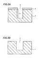
- the via hole 3 described above penetrates through the semiconductor substrate 1, the via hole 3 does not necessarily penetrate through the substrate 1 and its bottom may be located in the middle of the semiconductor substrate 1. Therefore, it is possible that the via hole 3 is formed partway in the semiconductor substrate 1 using the Bosch process as shown in Fig. 3A, and then the scallops 4 are improved as shown in Fig. 3B.
- FIGS. 4 through 13 are cross-sectional views showing the semiconductor device in a sequence of manufacturing process steps. Explanation on the same structure as in the first embodiment is omitted or simplified. Although the manufacturing process is applied to a wafer in which a plurality of the semiconductor devices is arrayed in a matrix bordered with predetermined dicing lines, only one of the semiconductor devices is described hereafter for the simplicity of explanation.
- a semiconductor substrate 5 in a top surface of which an electronic device (a CCD, a light-receiving device such as a CCD and an infrared sensor, a light-emitting device or other semiconductor device, for example) is formed.
- the semiconductor substrate 5 is 8 inches (200 mm) in diameter and 300-700 ⁇ m in thickness, for example.
- a first insulation film 6 (a silicon oxide film or a BPSG (Boro-Phospho Silicate Glass) film formed by thermal oxidation or CVD, for example) of a thickness of 2 ⁇ m, for example, is formed on the top surface of the semiconductor substrate 5.
- a metal layer such as aluminum (Al), aluminum alloy, copper (Cu) or the like is formed by sputtering, plating or other film forming method. After that, patterning is performed by etching the metal layer using a photoresist layer (not shown) as a mask. With this, a pad electrode 7 of a thickness of 1 ⁇ m, for example, is formed on the first insulation film 6. The pad electrode 7 is electrically connected with the electronic device and its peripheral element on the semiconductor substrate 5 through a wiring (not shown).
- a passivation film 8 (a silicon nitride film, for example) that covers a portion of the pad electrode 7 on the top surface of the semiconductor substrate 5 is formed by CVD, for example.
- a supporter 10 is bonded to the top surface of the semiconductor substrate 5 including the pad electrode 7 through an adhesive layer 9 made of an epoxy resin, resist, acryl or the like.
- the supporter 10 may be a film-shaped protection tape, may be a rigid substrate made of a glass, quartz, ceramics, plastics, a metal or the like, or may be made of a resin. It is preferable that the supporter 10 is a rigid substrate in order to firmly support the semiconductor substrate 5 of reducing thickness and to accommodate hands-free automatic transfer.
- the supporter 10 serves to support the semiconductor substrate 5 as well as protecting a surface of the device.
- back grinding by a back surface grinder is applied to a back surface of the semiconductor substrate 5 to reduce the thickness of the semiconductor substrate 5 down to a predetermined thickness (about 100-150 ⁇ m, for example).
- the back grinding may be replaced with etching, or a combination of grinding and etching.
- the back grinding might not be necessary, depending on usage or specifications of the final product or an initial thickness of the semiconductor substrate 5 being provided.
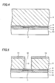
- a mask layer 11 is selectively formed on the back surface of the semiconductor substrate 5, as shown in Fig. 5.
- the mask layer 11 has an opening at a location on the back surface of the semiconductor substrate 5 corresponding to the pad electrode 7.
- the mask layer 11 may be an insulation film such as a silicon oxide film and a silicon nitride film, or a photoresist layer, as in the first embodiment.
- a predetermined region in the semiconductor substrate 5 is etched by the Bosch process using the mask layer 11 as a mask.
- Concrete processing conditions of the Bosch process are the same as those in the first embodiment.
- a via hole 12 (an opening) that penetrates through the semiconductor substrate 5 from the back surface to the top surface and exposes a portion of the first insulation film 6 is formed by the Bosch process
- a sidewall of the via hole 12 is shaped into scallops 13.
- a diameter of the via hole 12 is about 30-50 ⁇ m, and a depth of it is about 100-150 ⁇ m, for example.
- the mask layer 11 is removed.
- the mask layer 2 is the photoresist layer
- it is removed by O 2 plasma ashing, for example, using photoresist removal equipment such as a plasma asher.
- the mask layer 11 is the insulation film such as the silicon oxide film, it is removed using a parallel plate plasma etcher or a reactive ion etcher.
- the scallops 13 are removed by dry etching to flatten the sidewall of the via hole 12, as shown in Fig. 6. Examples of concrete processing conditions and equipment used in the process are the same as those in the first embodiment. Then the portion of the first insulation film 6 exposed in the via hole 12 is removed to expose the pad electrode 7.
- removing the portion of the first insulation film 6 can be performed at the same time as flattening the sidewall of the vial hole 12, using the same etching equipment. Furthermore, when the mask layer 11 is the insulation film such as the silicon oxide film, it is preferable that removing the mask layer 11, flattening the sidewall of the via hole 12 and removing the portion of the first insulation film 6 are performed simultaneously using the same equipment.
- a second insulation film 14 (a silicon oxide film or a silicon nitride film formed by CVD, for example) is formed over the entire back surface of the semiconductor substrate 5 including the sidewall of the via hole 12.
- the second insulation film 14 serves to isolate the semiconductor substrate 5 from conductive materials (a barrier layer 15, a seed layer 16, a through-hole electrode 17 and a wiring layer 18, that are to be described below).
- the second insulation film 14 in the bottom of the via hole 12 is removed by etching using a photoresist layer (not shown) as a mask, as shown in Fig. 8.
- a portion of the pad electrode 7 is exposed by the etching.
- the etching may be performed without the mask taking advantage of a varying thickness of the second insulation film 14, the thickness of which is greater on the back surface of the semiconductor substrate 5, reduces on the sidewall and further reduces toward the bottom of the via hole 12.
- the manufacturing process is optimized by not using the mask in the etching.
- the first insulation film 6 and the second insulation film 14 may be removed in the same etching process.
- the barrier layer 15 is formed on the sidewall of the via hole 12 and the back surface of the semiconductor substrate 5, as shown in Fig. 9.
- the barrier layer 15 is formed by sputtering, PVD (Physical Vapor Deposition), CVD or other film forming method.
- the barrier layer 15 is composed of a titanium (Ti) layer, a titanium nitride (TiN) layer, a tantalum (Ta) layer, a tantalum nitride (TaN) layer,'a titanium tungsten (TiW) layer, a tungsten nitride (WN) layer, a zirconium (Zr) layer, a zirconium nitride (ZrN) layer or the like.
- the barrier layer 15 serves to prevent diffusion of metallic material composing the through-hole electrode 17 to be formed in the via hole 12, to prevent inter reaction between the metallic material and an underlying conductor (the pad electrode 7 in this embodiment), and to improve adhesion of the through-hole electrode 17 to the semiconductor substrate 5, which will be described later.
- the barrier layer 15 is not limited to being formed of those specified materials as long as it serves as described above, and may be made of a single layer or stacked layers.
- the stacked layers are made of a combination of the materials mentioned above, such as the titanium layer / the titanium nitride layer, for example.
- the seed layer 16 is formed on the barrier layer 15, as shown in Fig. 9.
- the seed layer 16 is a conductive layer that serves as a foundation electrode to form the through-hole electrode 17 and the wiring layer 18 by plating as described below, and composed of a metal such as copper (Cu), ruthenium (Ru) or palladium (Pd).
- the seed layer 16 is formed by sputtering, PVD, CVD or other film forming method.
- a thickness of the seed layer 16 is about 50 nm, for example. Since the sidewall of the via hole 12 is flattened, the coverage of the barrier layer 15 and the seed layer 16 is better than that in the conventional art.
- the through-hole electrode 17 made of copper and the wiring layer 18 continuously connected with it are formed on the seed layer 16 including the inside of the via hole 12 by electrolytic plating using the seed layer 16 as a plating electrode, as shown in Fig. 9.
- the through-hole electrode 17 is a conductive layer formed inside the via hole 12.
- the through-hole electrode 17 and the wiring layer 18 are electrically connected with the pad electrode 7 exposed in the bottom of the via hole 12 through the barrier layer 15 and the seed layer 16. Since the sidewall of the via hole 12 is flattened, the charge convergence seen in the conventional art does not take place and the through-hole electrode 17 and the wiring layer 18 are formed favorably.
- the through-hole electrode 17 does not necessarily fill the via hole 12 completely, and may fill it incompletely as shown in Fig. 12.
- the conductive material needed to form the through-hole electrode 17 and the wiring layer 18 can be saved, while throughput is improved since the through-hole electrode 17 and the wiring layer 18 can be formed in less time compared with the case in which the via hole 12 is filled completely.
- unnecessary portions of the wiring layer 18 and the seed layer 16 are removed by etching using the photoresist layer 19 as a mask.
- the wiring layer 18 is shaped into the predetermined wiring pattern by the etching.
- the barrier layer 15 formed on the back surface of the semiconductor substrate 5 is selectively removed by etching using the wiring layer 18 as a mask.
- the barrier layer 15, the seed layer 16, the through-hole electrode 17 and the wiring layer 18 are not limited to be formed as described above.
- a photoresist layer or the like may be formed in a region on the back surface of the semiconductor substrate 5, where the barrier layer 15 and the wiring layer 18 are not to be formed, and patterning is performed by forming the barrier layer 15, the seed layer 16 and the wiring layer 18 in a region that is not covered with the photoresist layer or the like.
- the manufacturing process described above does not need the photoresist layer 19.
- a protection layer 20 made of an organic material such as solder resist or an inorganic material such as a silicon nitride film is formed on the back surface of the semiconductor substrate 5, as shown in Fig. 11.
- An opening is formed in a region of the protection layer 20 where a conductive terminal is to be formed, and an electrode connection layer (not shown) made of nickel (Ni) and gold (Au) is formed on the wiring layer 18 exposed in the opening.
- a solder is screen-printed on the electrode connection layer and ball-shaped conductive terminal 21 is formed by reflowing the solder by heat treatment.
- the conductive terminal 21 may be formed by a so-called dispenser method (a coating method) in which a ball-shaped terminal or the like made of a solder or the like is coated using a dispenser or by electrolytic plating or the like. Also, there is a case of other embodiment, in which the conductive terminal 21 is not formed. In this case, the electrode connection layer or the wiring layer 18 is exposed in the opening in the protection layer 20. And the electrode connection layer or the wiring layer 18 is connected with an electrode of another device.
- the supporter 10 may be left bonded to the semiconductor substrate 5, or separated from the semiconductor substrate 5 so that it can be recycled.
- the semiconductor device of a chip size package type in which a wiring from a lower layer conductor (the pad electrode 7) to an upper layer conductor (the wiring layer 18, the conductive terminal 21) provided on the back surface is implemented through the via hole 12.
- the semiconductor device When the semiconductor device is incorporated into electronic equipment, it is electrically connected with an external circuit by mounting the conductive terminal 21 on a wiring pattern on a circuit board.
- the scallops are caused on the sidewall of the via hole by the Bosch process, they are removed and flattened.
- desired film can be stably and homogeneously formed in the via hole 12, making it possible to improve the reliability and the yield of the semiconductor device.
- insufficient coverage is less likely to occur, each film on the sidewall of the via hole can be reduced in thickness to improve the productivity.
- the semiconductor devices are the BGA (Ball Grid Array) type semiconductor devices that have the ball-shaped conductive terminal 21 in the embodiments described above, the embodiments of this invention may be applied to semiconductor devices of other types such as LGA (Land Grid Array) type, CSP (Chip Size Package) type and flip-chip type that have no ball-shaped conductive terminal.
- BGA Ball Grid Array
- CSP Chip Size Package
- the supporter is bonded to the top surface (device side surface) of the semiconductor substrate 5 in the embodiments described above, the supporter 10 may be bonded to the other surface (non-device side surface) as shown in Fig. 13 to manufacture a desired semiconductor device.
- the pad electrode 7, the wiring 18, the conductive terminal 21 and the like are formed on the top surface (device side surface) of the semiconductor substrate 5 in this semiconductor device.
- the semiconductor device is incorporated into electronic equipment, it is electrically connected with an external circuit by mounting the conductive terminal 21 on a wiring pattern on a circuit board.
- an opening is formed in an insulation film 30 (a silicon oxide film formed by CVD, for example) on the back surface of the semiconductor substrate 5 at a location corresponding to the through-hole electrode 17 after the supporter 10 is separated and removed, and a conductive terminal of another semiconductor device is connected to the opening to implement stacked layers of the semiconductor devices.
- an insulation film 30 a silicon oxide film formed by CVD, for example
- the manufacturing methods of the semiconductor devices according to the embodiments of this invention reduce scallops generated on the sidewall of via holes formed in a semiconductor device. As a result, it is made possible to form a highly homogeneous film in the via holes in the process steps after the flattening of the inside via hole surfaces.
Landscapes
- Internal Circuitry In Semiconductor Integrated Circuit Devices (AREA)
- Drying Of Semiconductors (AREA)
Abstract
Description
- This invention relates to a manufacturing method of a semiconductor device, specifically to a manufacturing method of a semiconductor device having an opening in a semiconductor substrate.
- It is known that a via hole (opening) is formed to penetrate through a semiconductor substrate from one of principal surfaces of the semiconductor substrate to the other and a conductive material (metal such as aluminum, copper, tungsten and titanium tungsten) serving as a wiring is formed in the via hole so that conductors disposed on both of the principal surfaces are electrically connect with each other.
- Bosch process has been known as one of methods to form the via hole. The Bosch process is used to produce a deep vertical trench in the semiconductor substrate and consists of two periodically alternating processes, which are a plasma etch process in which a surface of the semiconductor substrate is plasma etched isotropically using a SF6 gas and a plasma deposition process in which carbon polymers are deposited as a protection film using a C4F8 gas on a sidewall of the trench formed by the plasma etch process.
- When the plasma etch process is performed by the Bosch process, a
via hole 101 is formed to penetrate asemiconductor substrate 100, as shown in Fig. 14. It is known, however, that rough shapes (hereafter referred to as scallops 102) are caused on a surface of a sidewall of thevia hole 101 at the same time. Thescallops 102 result from the isotropic etching in the plasma etch process. - The technology mentioned above is described in
Japanese Patent Application Publication No. 2006-12889 - When the surface of the sidewall of the
via hole 101 is turned to thescallops 102, it is difficult to form a desired film (an insulation film or a barrier layer, for example) homogeneously on the sidewall of thevia hole 101, thereby causing a problem that is reduction in yield and reliability of the semiconductor device. - To describe concretely, when an
insulation film 103 is formed on the sidewall of thevia hole 101 and a barrier layer 104 (a titanium layer, a titanium-tungsten layer, a tantalum layer or a tantalum nitride layer, for example) or a conductive material serving as a wiring is to be deposited on theinsulation film 103 by sputtering as shown in Fig 15A, for example, there has been a region to which sputtered particles do not reach sufficiently because of thescallops 102, thereby making the sputtered layer uneven in thickness and insufficient in coverage. Particularly when an aspect ratio (height / aperture diameter) of thevia hole 101 is high, forming a homogeneous film becomes even more difficult, resulting in reduced functionality of thebarrier layer 104 and the wiring. - Similarly, when the
barrier layer 104 or the conductive material serving as the wiring is formed by CVD (Chemical Vapor Deposition), a reaction gas does not reach evenly to the sidewall of thevia hole 101 because of thescallops 102, and there has been a region where the layer deposited by CVD becomes insufficient in coverage. - In addition, there is a case in which the film is formed thicker than usually required in order to avoid the insufficient coverage, which causes problems of reduced productivity and an excessive thickness of the film in a specific region.
- Also, the
scallops 102 have sharp edges which are to be reflected in a film formed in thevia hole 101 in a later process step. As a result, when theinsulation film 103, thebarrier layer 104 and aseed layer 105 that serves as a plating electrode are formed consecutively in thevia hole 101 and a through-hole electrode 106 is formed in thevia hole 101 by plating as shown in Fig. 15B, electric charge convergence is caused at thesharp edges 107 of theseed layer 105 in the plating process. Then a material (copper or aluminum, for example) forming the through-hole electrode 106 grows abnormally at thesharp edges 107 to form abnormally grownportions 108 as shown in Fig. 15B. Since the abnormally grownportions 108 touch the material forming the through-hole electrode 106 on the opposite side when they grow further, appropriate plating is not performed and there are caused problems that the through-hole electrode 106 is disconnected and a void is caused in the through-hole electrode 106. - Reducing etch rate in the Bosch process could suppress generation of the
scallops 102. However, it causes a problem of reduced productivity. - This invention is directed to offer a manufacturing method of a semiconductor device, which makes it possible even when the scallops are caused in the process to form the via hole using the Bosch process that practically homogeneous films are formed in the via hole in later process steps.
- It is an object of this invention to provide an improved manufacturing method of semiconductor devices that lessens this drawback.
- The solution according to the invention lies in the features of the independent claims and preferably in these of the dependent claims.
- This invention is directed to solve the problems addressed above and has following features. This invention offers a method of manufacturing a semiconductor device including a plasma etch process to form a groove in a semiconductor substrate, a plasma deposition process to deposit a protection film on a sidewall of the groove, a process to form an opening in the semiconductor substrate by alternating the plasma etch process and the plasma deposition process and a process to flatten a sidewall of the opening in the semiconductor substrate.
- This invention also offers a method of manufacturing a semiconductor device including providing a semiconductor substrate having a pad electrode formed on one of principal surfaces of the semiconductor substrate through an insulation film, a process to form a mask layer on another of the principal surfaces of the semiconductor substrate having an opening at a location corresponding to the pad electrode, a plasma etch process to form a groove in the semiconductor substrate using the mask layer as a mask, a plasma deposition process to deposit a protection film on a sidewall of the groove, a process to form an opening reaching the insulation film in the semiconductor substrate by alternating the plasma etch process and the plasma deposition process and a process to flatten a sidewall of the opening in the semiconductor substrate.
- This invention also offers the manufacturing method of the semiconductor device further including a process to remove the mask layer and a process to remove the insulation film to expose the pad electrode at a bottom of the via hole, wherein the process to remove the mask layer, the process to remove the insulation film and the process to flatten the sidewall of the opening in the semiconductor substrate are performed simultaneously.
- The Bosch process comprises two alternating processes, which are a plasma etch process in which a surface of the semiconductor substrate is plasma etched (preferably isotropically using a SF6 gas and a plasma deposition process in which a protection film is depicted (preferably using a C4F8 gas) on a sidewall of the hole formed by the plasma etching.
-
- Fig. 1 is a cross-sectional view showing a manufacturing method of a semiconductor device according a first embodiment of this invention.
- Fig. 2 is a cross-sectional view showing the manufacturing method of the semiconductor device according the first embodiment of this invention.
- Figs. 3A and 3B are cross-sectional views showing the manufacturing method of the semiconductor device according the first embodiment of this invention.
- Fig. 4 is a cross-sectional view showing a manufacturing method of a semiconductor device according a second embodiment of this invention.
- Fig. 5 is a cross-sectional view showing the manufacturing method of the semiconductor device according the second embodiment of this invention.
- Fig. 6 is a cross-sectional view showing the manufacturing method of the semiconductor device according the second embodiment of this invention.
- Fig. 7 is a cross-sectional view showing the manufacturing method of the semiconductor device according the second embodiment of this invention.
- Fig. 8 is a cross-sectional view showing the manufacturing method of the semiconductor device according the second embodiment of this invention.
- Fig. 9 is a cross-sectional view showing the manufacturing method of the semiconductor device according the second embodiment of this invention.
- Fig. 10 is a cross-sectional view showing the manufacturing method of the semiconductor device according the second embodiment of this invention.
- Fig. 11 is a cross-sectional view showing the semiconductor device and its manufacturing method according to the second embodiment of this invention.
Fig. 12 is a cross-sectional view showing the manufacturing method of the semiconductor device according the second embodiment of this invention. - Fig. 13 is a cross-sectional view showing the manufacturing method of the semiconductor device according the second embodiment of this invention.
- Fig. 14 is a cross-sectional view showing a manufacturing method of a semiconductor device according to a conventional art.
- Figs. 15A and 15B are cross-sectional views showing the manufacturing method of the semiconductor device according to the conventional art.
- Embodiments of this invention will be explained hereinafter, referring to the drawings. Figs. 1 through 3B are cross-sectional views showing a manufacturing method of a semiconductor device according to a first embodiment of this invention.
- First, a
semiconductor substrate 1, on a surface of which an electronic device (not shown) is formed, is provided as shown in Fig. 1. Next, amask layer 2 is selectively formed on a back surface of thesemiconductor substrate 1. Themask layer 2 is used as a mask to form avia hole 3 and its material is not limited to a particular material as long as it functions for that purpose. Themask layer 2 may be an insulation film such as a silicon oxide film and a silicon nitride film or a photoresist layer. - Next, a predetermined region in the
semiconductor substrate 1 is etched by the Bosch process using themask layer 2 as a mask. To describe concretely, the etching is performed using a BM2304 type ICP (Inductively Coupled Plasma) etcher by alternating a plasma etch process at a pressure of 50-60 mTorr, a SF6 gas flow rate of 400-450 scc/min, an O2 gas flow rate of 35-40 scc/min and an ICP power of 1500-2000 W for 10 seconds and a plasma deposition process at a pressure of 20-30 mTorr, a C4F8 gas flow rate of 150-200 scc/min and an ICP power of 1200-1700 W for 5 seconds. - While the via hole (opening) 3 penetrating through a thickness of the
semiconductor substrate 1 is formed by the Bosch process, a surface of a sidewall of thevia hole 3 is shaped into scallops 4, as shown in Fig. 1. A depth of thevia hole 3 is about 100-150 µm, for example, and a step height of the scallops 4 is about 6000 Å, for example. The step height of the scallops 4 becomes larger as an amount of side etching in a lateral direction by the SF6 gas increases. - The shape of the scallops 4 in the figure is considerably exaggerated for the sake of viewing convenience and does not reflect the real dimension. The closer to a bottom of the via hole 3 (lower side in Fig. 1) a location is, the lower an etch rate of the plasma etch at the location is.
- Therefore, the step height of the scallops 4 is smaller and closer to flat at a location closer to the bottom of the
via hole 3 than that at a location in upper side of the via hole 3 (upper side in Fig. 1). The viahole 3 is shown to have a straight shape in Fig. 1. However, the actual viahole 3 formed by the Bosch process tends to be tapered down, that is, a diameter of the opening reduces as the depth of the viahole 3 becomes greater. - Next, the
mask layer 2 is removed. To describe concretely, when themask layer 2 is a photoresist layer, it is removed by O2 plasma ashing using photoresist removal equipment such as a plasma asher. When themask layer 2 is an insulation film such as a silicon oxide film, it is removed using a parallel plate plasma etcher or a reactive ion etcher. - Then the scallops 4 are removed by dry etching to flatten (i.e., to smooth) the sidewall of the via
hole 3, as shown in Fig. 2. The dry etching is an etching method using ions and radicals generated in plasma that is generated in a chamber of the equipment. The dry etching includes plasma etching, reactive ion etching, chemical dry etching and the like. - It is performed using a parallel plate plasma etcher, for example. The scallops 4 were reduced by executing the flattening process at a pressure of 50-150 mTorr, a CF4 gas flow rate of 50-100 scc/min, a CHF3 gas flow rate of 0-25 scc/min and a power of 400-800 W. Performing the etching under the conditions of lower pressure, higher power and richer CF4 gas is preferable from a standpoint of enhancing an effect of improving the scallops 4, that is, making the sidewall of the via
hole 3 flatter. - Then an insulation film, a barrier layer, a seed layer and a through-hole electrode are formed on the flattened sidewall of the via
hole 3, making it possible to electrically connect one of principal surfaces of thesemiconductor substrate 1 with the other. Detailed manufacturing processes after the flattening process will be described in explanation of a second embodiment. - The scallops 4 on the sidewall of the via
hole 3 are improved in this embodiment. As a result, it is made possible to form a highly homogeneous film in the viahole 3 in later process steps. In a sputtering process, for example, homogenizing a deposited amount of sputtered particles onto the sidewall of the viahole 3 can be facilitated. Also, in the case of CVD, a reaction gas reaches the sidewall evenly, making it possible to prevent insufficient coverage. - In addition, excessive film forming is no longer needed because possibility of insufficient coverage due to the scallops 4 has been eliminated. Thus the productivity is improved and a thickness of the film formed in the via
hole 3 can be reduced. - The scallops 4 do not affect film forming in later process steps, and electric charges do not converge in a plating process. As a result, highly reliable plating is made possible. Since all films formed on the sidewall of the via
hole 3 are formed favorably, the reliability and the yield are-improved compared with the conventional semiconductor device. - Although the via
hole 3 described above penetrates through thesemiconductor substrate 1, the viahole 3 does not necessarily penetrate through thesubstrate 1 and its bottom may be located in the middle of thesemiconductor substrate 1. Therefore, it is possible that the viahole 3 is formed partway in thesemiconductor substrate 1 using the Bosch process as shown in Fig. 3A, and then the scallops 4 are improved as shown in Fig. 3B. - Next, a manufacturing process of a semiconductor device according to the second embodiment of this invention will be explained referring to the drawings. Figs. 4 through 13 are cross-sectional views showing the semiconductor device in a sequence of manufacturing process steps. Explanation on the same structure as in the first embodiment is omitted or simplified. Although the manufacturing process is applied to a wafer in which a plurality of the semiconductor devices is arrayed in a matrix bordered with predetermined dicing lines, only one of the semiconductor devices is described hereafter for the simplicity of explanation.
- First, as shown in Fig. 4, there is provided a
semiconductor substrate 5, in a top surface of which an electronic device (a CCD, a light-receiving device such as a CCD and an infrared sensor, a light-emitting device or other semiconductor device, for example) is formed. Thesemiconductor substrate 5 is 8 inches (200 mm) in diameter and 300-700 µm in thickness, for example. A first insulation film 6 (a silicon oxide film or a BPSG (Boro-Phospho Silicate Glass) film formed by thermal oxidation or CVD, for example) of a thickness of 2 µm, for example, is formed on the top surface of thesemiconductor substrate 5. - A metal layer such as aluminum (Al), aluminum alloy, copper (Cu) or the like is formed by sputtering, plating or other film forming method. After that, patterning is performed by etching the metal layer using a photoresist layer (not shown) as a mask. With this, a
pad electrode 7 of a thickness of 1 µm, for example, is formed on thefirst insulation film 6. Thepad electrode 7 is electrically connected with the electronic device and its peripheral element on thesemiconductor substrate 5 through a wiring (not shown). - Next, a passivation film 8 (a silicon nitride film, for example) that covers a portion of the
pad electrode 7 on the top surface of thesemiconductor substrate 5 is formed by CVD, for example. Next, asupporter 10 is bonded to the top surface of thesemiconductor substrate 5 including thepad electrode 7 through anadhesive layer 9 made of an epoxy resin, resist, acryl or the like. Thesupporter 10 may be a film-shaped protection tape, may be a rigid substrate made of a glass, quartz, ceramics, plastics, a metal or the like, or may be made of a resin. It is preferable that thesupporter 10 is a rigid substrate in order to firmly support thesemiconductor substrate 5 of reducing thickness and to accommodate hands-free automatic transfer. Thesupporter 10 serves to support thesemiconductor substrate 5 as well as protecting a surface of the device. - Next, back grinding by a back surface grinder is applied to a back surface of the
semiconductor substrate 5 to reduce the thickness of thesemiconductor substrate 5 down to a predetermined thickness (about 100-150 µm, for example). The back grinding may be replaced with etching, or a combination of grinding and etching. The back grinding might not be necessary, depending on usage or specifications of the final product or an initial thickness of thesemiconductor substrate 5 being provided. - Next, a
mask layer 11 is selectively formed on the back surface of thesemiconductor substrate 5, as shown in Fig. 5. Themask layer 11 has an opening at a location on the back surface of thesemiconductor substrate 5 corresponding to thepad electrode 7. Themask layer 11 may be an insulation film such as a silicon oxide film and a silicon nitride film, or a photoresist layer, as in the first embodiment. - Next, a predetermined region in the
semiconductor substrate 5 is etched by the Bosch process using themask layer 11 as a mask. Concrete processing conditions of the Bosch process are the same as those in the first embodiment. - While a via hole 12 (an opening) that penetrates through the
semiconductor substrate 5 from the back surface to the top surface and exposes a portion of thefirst insulation film 6 is formed by the Bosch process, a sidewall of the viahole 12 is shaped intoscallops 13. A diameter of the viahole 12 is about 30-50 µm, and a depth of it is about 100-150 µm, for example. - Next, the
mask layer 11 is removed. To describe concretely, when themask layer 2 is the photoresist layer, it is removed by O2 plasma ashing, for example, using photoresist removal equipment such as a plasma asher. When themask layer 11 is the insulation film such as the silicon oxide film, it is removed using a parallel plate plasma etcher or a reactive ion etcher. - Then the
scallops 13 are removed by dry etching to flatten the sidewall of the viahole 12, as shown in Fig. 6. Examples of concrete processing conditions and equipment used in the process are the same as those in the first embodiment. Then the portion of thefirst insulation film 6 exposed in the viahole 12 is removed to expose thepad electrode 7. - Note that removing the portion of the
first insulation film 6 can be performed at the same time as flattening the sidewall of thevial hole 12, using the same etching equipment. Furthermore, when themask layer 11 is the insulation film such as the silicon oxide film, it is preferable that removing themask layer 11, flattening the sidewall of the viahole 12 and removing the portion of thefirst insulation film 6 are performed simultaneously using the same equipment. - Next, a second insulation film 14 (a silicon oxide film or a silicon nitride film formed by CVD, for example) is formed over the entire back surface of the
semiconductor substrate 5 including the sidewall of the viahole 12. Thesecond insulation film 14 serves to isolate thesemiconductor substrate 5 from conductive materials (abarrier layer 15, aseed layer 16, a through-hole electrode 17 and awiring layer 18, that are to be described below). - Next, the
second insulation film 14 in the bottom of the viahole 12 is removed by etching using a photoresist layer (not shown) as a mask, as shown in Fig. 8. A portion of thepad electrode 7 is exposed by the etching. The etching may be performed without the mask taking advantage of a varying thickness of thesecond insulation film 14, the thickness of which is greater on the back surface of thesemiconductor substrate 5, reduces on the sidewall and further reduces toward the bottom of the viahole 12. The manufacturing process is optimized by not using the mask in the etching. Also, thefirst insulation film 6 and thesecond insulation film 14 may be removed in the same etching process. - Next, the
barrier layer 15 is formed on the sidewall of the viahole 12 and the back surface of thesemiconductor substrate 5, as shown in Fig. 9. Thebarrier layer 15 is formed by sputtering, PVD (Physical Vapor Deposition), CVD or other film forming method. Thebarrier layer 15 is composed of a titanium (Ti) layer, a titanium nitride (TiN) layer, a tantalum (Ta) layer, a tantalum nitride (TaN) layer,'a titanium tungsten (TiW) layer, a tungsten nitride (WN) layer, a zirconium (Zr) layer, a zirconium nitride (ZrN) layer or the like. Thebarrier layer 15 serves to prevent diffusion of metallic material composing the through-hole electrode 17 to be formed in the viahole 12, to prevent inter reaction between the metallic material and an underlying conductor (thepad electrode 7 in this embodiment), and to improve adhesion of the through-hole electrode 17 to thesemiconductor substrate 5, which will be described later. Thebarrier layer 15 is not limited to being formed of those specified materials as long as it serves as described above, and may be made of a single layer or stacked layers. The stacked layers are made of a combination of the materials mentioned above, such as the titanium layer / the titanium nitride layer, for example. - Next, the
seed layer 16 is formed on thebarrier layer 15, as shown in Fig. 9. Theseed layer 16 is a conductive layer that serves as a foundation electrode to form the through-hole electrode 17 and thewiring layer 18 by plating as described below, and composed of a metal such as copper (Cu), ruthenium (Ru) or palladium (Pd). Theseed layer 16 is formed by sputtering, PVD, CVD or other film forming method. A thickness of theseed layer 16 is about 50 nm, for example. Since the sidewall of the viahole 12 is flattened, the coverage of thebarrier layer 15 and theseed layer 16 is better than that in the conventional art. - Next, the through-
hole electrode 17 made of copper and thewiring layer 18 continuously connected with it are formed on theseed layer 16 including the inside of the viahole 12 by electrolytic plating using theseed layer 16 as a plating electrode, as shown in Fig. 9. The through-hole electrode 17 is a conductive layer formed inside the viahole 12. The through-hole electrode 17 and thewiring layer 18 are electrically connected with thepad electrode 7 exposed in the bottom of the viahole 12 through thebarrier layer 15 and theseed layer 16. Since the sidewall of the viahole 12 is flattened, the charge convergence seen in the conventional art does not take place and the through-hole electrode 17 and thewiring layer 18 are formed favorably. - Note that the through-
hole electrode 17 does not necessarily fill the viahole 12 completely, and may fill it incompletely as shown in Fig. 12. With a structure described above, the conductive material needed to form the through-hole electrode 17 and thewiring layer 18 can be saved, while throughput is improved since the through-hole electrode 17 and thewiring layer 18 can be formed in less time compared with the case in which the viahole 12 is filled completely. - Next, a
photoresist layer 19, that is used to shape thewiring layer 18 into a wiring pattern, is formed selectively on thewiring layer 18 on the back surface of thesemiconductor substrate 5, as shown in Fig. 10. Next, unnecessary portions of thewiring layer 18 and theseed layer 16 are removed by etching using thephotoresist layer 19 as a mask. Thewiring layer 18 is shaped into the predetermined wiring pattern by the etching. Following the above, thebarrier layer 15 formed on the back surface of thesemiconductor substrate 5 is selectively removed by etching using thewiring layer 18 as a mask. - The
barrier layer 15, theseed layer 16, the through-hole electrode 17 and thewiring layer 18 are not limited to be formed as described above. For example, a photoresist layer or the like may be formed in a region on the back surface of thesemiconductor substrate 5, where thebarrier layer 15 and thewiring layer 18 are not to be formed, and patterning is performed by forming thebarrier layer 15, theseed layer 16 and thewiring layer 18 in a region that is not covered with the photoresist layer or the like. The manufacturing process described above does not need thephotoresist layer 19. - Next, a
protection layer 20 made of an organic material such as solder resist or an inorganic material such as a silicon nitride film is formed on the back surface of thesemiconductor substrate 5, as shown in Fig. 11. An opening is formed in a region of theprotection layer 20 where a conductive terminal is to be formed, and an electrode connection layer (not shown) made of nickel (Ni) and gold (Au) is formed on thewiring layer 18 exposed in the opening. After that, a solder is screen-printed on the electrode connection layer and ball-shapedconductive terminal 21 is formed by reflowing the solder by heat treatment. - The
conductive terminal 21 may be formed by a so-called dispenser method (a coating method) in which a ball-shaped terminal or the like made of a solder or the like is coated using a dispenser or by electrolytic plating or the like. Also, there is a case of other embodiment, in which theconductive terminal 21 is not formed. In this case, the electrode connection layer or thewiring layer 18 is exposed in the opening in theprotection layer 20. And the electrode connection layer or thewiring layer 18 is connected with an electrode of another device. - The
supporter 10 may be left bonded to thesemiconductor substrate 5, or separated from thesemiconductor substrate 5 so that it can be recycled. - With the processing steps described above, there is completed the semiconductor device of a chip size package type in which a wiring from a lower layer conductor (the pad electrode 7) to an upper layer conductor (the
wiring layer 18, the conductive terminal 21) provided on the back surface is implemented through the viahole 12. When the semiconductor device is incorporated into electronic equipment, it is electrically connected with an external circuit by mounting theconductive terminal 21 on a wiring pattern on a circuit board. - According to the first and second embodiments, as described above, even when the scallops are caused on the sidewall of the via hole by the Bosch process, they are removed and flattened. As a result, desired film can be stably and homogeneously formed in the via
hole 12, making it possible to improve the reliability and the yield of the semiconductor device. Also, since insufficient coverage is less likely to occur, each film on the sidewall of the via hole can be reduced in thickness to improve the productivity. - Although the semiconductor devices are the BGA (Ball Grid Array) type semiconductor devices that have the ball-shaped conductive terminal 21 in the embodiments described above, the embodiments of this invention may be applied to semiconductor devices of other types such as LGA (Land Grid Array) type, CSP (Chip Size Package) type and flip-chip type that have no ball-shaped conductive terminal.
- Also, this invention is not limited to the embodiments described above and may be modified within the scope of the invention.
- For example, although the supporter is bonded to the top surface (device side surface) of the
semiconductor substrate 5 in the embodiments described above, thesupporter 10 may be bonded to the other surface (non-device side surface) as shown in Fig. 13 to manufacture a desired semiconductor device. Thepad electrode 7, thewiring 18, theconductive terminal 21 and the like are formed on the top surface (device side surface) of thesemiconductor substrate 5 in this semiconductor device. When the semiconductor device is incorporated into electronic equipment, it is electrically connected with an external circuit by mounting theconductive terminal 21 on a wiring pattern on a circuit board. It is also possible that an opening is formed in an insulation film 30 (a silicon oxide film formed by CVD, for example) on the back surface of thesemiconductor substrate 5 at a location corresponding to the through-hole electrode 17 after thesupporter 10 is separated and removed, and a conductive terminal of another semiconductor device is connected to the opening to implement stacked layers of the semiconductor devices. Note that the same structures in Fig. 13 as those already described above are denoted by the same symbols and explanations on them are omitted. The supporter may be bonded to either surface of the semiconductor substrate as described above. The embodiments of this invention can be broadly applied to semiconductor devices having a via hole. - The manufacturing methods of the semiconductor devices according to the embodiments of this invention reduce scallops generated on the sidewall of via holes formed in a semiconductor device. As a result, it is made possible to form a highly homogeneous film in the via holes in the process steps after the flattening of the inside via hole surfaces.
Claims (11)
- A method of manufacturing a semiconductor device, comprising:providing a semiconductor substrate (1);forming a hole (3) in the substrate (1) using a Bosch process; andreducing a surface roughness of a sidewall of the hole (3).
- A method of manufacturing a semiconductor device, comprising:providing a semiconductor substrate (1);forming a hole (3) in the substrate (1) by alternating aplasma etching and a plasma deposition; andsmoothing a sidewall of the hole (3) after the formation of the hole (3).
- The method of claim 2, further comprising forming an insulation film on the sidewall of the hole (3) and forming a conductive layer on the insulation film.
- The method of claim 2 or 3, wherein the smoothing of the sidewall comprises a dry etching.
- The method of claims 1, 2 or 3 wherein the smoothing of the sidewall comprises an etching using an etching gas comprising a CF4 gas.
- A method of manufacturing a semiconductor device, comprising:providing a semiconductor substrate (5) comprising a first surface, a second surface opposite from the first surface, an insulation film (6) formed on the first surface and a pad electrode (7) disposed on the insulation film (6);forming a mask layer (11) on the second surface so that an opening is formed in the mask layer (11) at a location corresponding to the pad electrode (7);providing an apparatus configured to perform a plasma etching to etch the substrate (5) and a plasma deposition to deposit a protection film;forming a via hole (12) in the substrate (5) using the mask layer (11) so as to expose the insulation film (6) by alternating the plasma etching and the plasma deposition using the apparatus; andreducing a surface roughness of a sidewall of the via hole (12) after the formation of the via hole (12).
- The method of claim 6, further comprising removing the mask layer (11) after the formation of the via hole (12) and before the reducing of the surface roughness.
- The method of claim 6, further comprising removing the mask layer (11), removing the insulation film (6) to expose the pad electrode (7) at a bottom of the hole (12), wherein the removing of the mask layer (11), the removing of the insulation film (6) and the reducing of the surface roughness are performed simultaneously.
- The method according to any of claims 6 to 8, further comprising forming a conductive layer (17) in the via hole (12) so as to be electrically connected with the pad electrode (7).
- The method according to any of claims 6 to 9, wherein the reducing of the surface roughness comprises a dry etching.
- The method according to any of claims 6 to 9, wherein the reducing of the surface roughness comprises an etching using an etching gas comprising a CF4 gas.
Applications Claiming Priority (1)
| Application Number | Priority Date | Filing Date | Title |
|---|---|---|---|
| JP2006139693A JP4812512B2 (en) | 2006-05-19 | 2006-05-19 | Manufacturing method of semiconductor device |
Publications (2)
| Publication Number | Publication Date |
|---|---|
| EP1858063A2 true EP1858063A2 (en) | 2007-11-21 |
| EP1858063A3 EP1858063A3 (en) | 2010-04-28 |
Family
ID=38420530
Family Applications (1)
| Application Number | Title | Priority Date | Filing Date |
|---|---|---|---|
| EP07010073A Withdrawn EP1858063A3 (en) | 2006-05-19 | 2007-05-21 | Manufacturing method of semiconductor device |
Country Status (6)
| Country | Link |
|---|---|
| US (1) | US8669183B2 (en) |
| EP (1) | EP1858063A3 (en) |
| JP (1) | JP4812512B2 (en) |
| KR (1) | KR100864777B1 (en) |
| CN (1) | CN101075554B (en) |
| TW (1) | TWI365508B (en) |
Cited By (3)
| Publication number | Priority date | Publication date | Assignee | Title |
|---|---|---|---|---|
| EP2048923A3 (en) * | 2007-10-09 | 2010-12-08 | Shinko Electric Industries Co., Ltd. | Method of manufacturing silicon substrate with a conductive through-hole |
| US20220301879A1 (en) * | 2020-09-25 | 2022-09-22 | Taiwan Semiconductor Manufacturing Company, Ltd. | High aspect ratio bosch deep etch |
| US20240395615A1 (en) * | 2023-05-25 | 2024-11-28 | Samsung Electronics Co., Ltd. | Semiconductor device and method of manufacturing the same |
Families Citing this family (58)
| Publication number | Priority date | Publication date | Assignee | Title |
|---|---|---|---|---|
| JP5143382B2 (en) * | 2006-07-27 | 2013-02-13 | オンセミコンダクター・トレーディング・リミテッド | Semiconductor device and manufacturing method thereof |
| JP5117062B2 (en) * | 2007-02-08 | 2013-01-09 | 株式会社フジクラ | Manufacturing method of semiconductor device |
| US20090017576A1 (en) * | 2007-07-09 | 2009-01-15 | Swarnal Borthakur | Semiconductor Processing Methods |
| CN101459066B (en) | 2007-12-13 | 2010-08-11 | 中芯国际集成电路制造(上海)有限公司 | Method for forming gate, shallow trench isolation region, and method for planarizing etched surface of silicon substrate |
| CN101911257B (en) * | 2008-01-23 | 2012-03-07 | 日矿金属株式会社 | ULSI micro-interconnect member having ruthenium electroplating layer on barrier layer |
| DE102008001952A1 (en) * | 2008-05-23 | 2009-11-26 | Robert Bosch Gmbh | Method for producing isolated micromechanical components arranged on a silicon substrate and components produced therefrom |
| US8132321B2 (en) * | 2008-08-13 | 2012-03-13 | Unimicron Technology Corp. | Method for making embedded circuit structure |
| US9039908B2 (en) * | 2008-08-27 | 2015-05-26 | Applied Materials, Inc. | Post etch reactive plasma milling to smooth through substrate via sidewalls and other deeply etched features |
| JP5350859B2 (en) * | 2009-03-30 | 2013-11-27 | シチズンホールディングス株式会社 | OPTICAL MEMBER, OPTICAL DEVICE MANUFACTURING METHOD, AND OPTICAL DEVICE |
| JP2010263145A (en) * | 2009-05-11 | 2010-11-18 | Panasonic Corp | Semiconductor device and manufacturing method thereof |
| KR20110000960A (en) | 2009-06-29 | 2011-01-06 | 삼성전자주식회사 | Semiconductor chip, stack module, memory card and manufacturing method thereof |
| TWI435386B (en) * | 2009-07-21 | 2014-04-21 | 愛發科股份有限公司 | Film surface treatment method |
| EP2306506B1 (en) * | 2009-10-01 | 2013-07-31 | ams AG | Method of producing a semiconductor device having a through-wafer interconnect |
| JP5532394B2 (en) | 2009-10-15 | 2014-06-25 | セイコーエプソン株式会社 | Semiconductor device, circuit board, and electronic equipment |
| KR20110139550A (en) | 2010-06-23 | 2011-12-29 | 삼성전자주식회사 | Method of forming a semiconductor device |
| CN102315157A (en) * | 2010-08-11 | 2012-01-11 | 上海集成电路研发中心有限公司 | Method for forming and correcting TSV (through silicon via) |
| US8659152B2 (en) * | 2010-09-15 | 2014-02-25 | Osamu Fujita | Semiconductor device |
| US8847400B2 (en) | 2010-09-15 | 2014-09-30 | Ps4 Luxco S.A.R.L. | Semiconductor device, method for manufacturing the same, and data processing device |
| EP2463896B1 (en) * | 2010-12-07 | 2020-04-15 | IMEC vzw | Method for forming through-substrate vias surrounded by isolation trenches with an airgap and corresponding device |
| CN102130045B (en) * | 2010-12-31 | 2015-12-02 | 上海集成电路研发中心有限公司 | Processing method of through holes |
| JP2012178520A (en) * | 2011-02-28 | 2012-09-13 | Elpida Memory Inc | Semiconductor apparatus and manufacturing method thereof |
| US8871105B2 (en) * | 2011-05-12 | 2014-10-28 | Lam Research Corporation | Method for achieving smooth side walls after Bosch etch process |
| KR101867998B1 (en) * | 2011-06-14 | 2018-06-15 | 삼성전자주식회사 | Method of forming a pattern |
| CN103050434B (en) * | 2011-10-17 | 2015-09-02 | 中芯国际集成电路制造(上海)有限公司 | The lithographic method of silicon through hole |
| CN102403217B (en) * | 2011-11-11 | 2013-11-06 | 华中科技大学 | Preparation method for ultrathin chip |
| JP5957926B2 (en) * | 2012-02-09 | 2016-07-27 | セイコーエプソン株式会社 | Manufacturing method of semiconductor device |
| CN102610560B (en) * | 2012-03-21 | 2014-03-05 | 中微半导体设备(上海)有限公司 | Method for modifying appearances of side walls of through holes |
| JP5916105B2 (en) * | 2012-03-27 | 2016-05-11 | 国立大学法人九州工業大学 | Manufacturing method of semiconductor device |
| CN102738074B (en) * | 2012-07-05 | 2014-07-02 | 中微半导体设备(上海)有限公司 | Method for forming semiconductor structure |
| JP5955706B2 (en) * | 2012-08-29 | 2016-07-20 | ルネサスエレクトロニクス株式会社 | Semiconductor device and manufacturing method thereof |
| JP2014063866A (en) * | 2012-09-21 | 2014-04-10 | Canon Inc | Method for processing silicon substrate and method for manufacturing charged particle beam lens |
| CN103117203B (en) * | 2013-03-08 | 2016-08-10 | 中微半导体设备(上海)有限公司 | The processing means of a kind of plasma etch process and method |
| CN104425357B (en) * | 2013-08-27 | 2017-12-01 | 中芯国际集成电路制造(上海)有限公司 | The forming method of dual-damascene structure |
| US9224615B2 (en) * | 2013-09-11 | 2015-12-29 | Taiwan Semiconductor Manufacturing Co., Ltd. | Noble gas bombardment to reduce scallops in bosch etching |
| CN104576506A (en) * | 2013-10-22 | 2015-04-29 | 中微半导体设备(上海)有限公司 | Method for etching silicon through hole |
| CN104617033B (en) * | 2013-11-05 | 2018-09-14 | 中芯国际集成电路制造(上海)有限公司 | Wafer-level packaging method |
| JP2015153978A (en) * | 2014-02-18 | 2015-08-24 | キヤノン株式会社 | Manufacturing method of through wiring |
| CN105720003B (en) * | 2014-12-03 | 2019-01-18 | 北京北方华创微电子装备有限公司 | Deep silicon hole lithographic method |
| CN105845650B (en) * | 2015-01-12 | 2018-10-23 | 中芯国际集成电路制造(上海)有限公司 | A kind of through-silicon via structure and preparation method thereof |
| JP2016174101A (en) * | 2015-03-17 | 2016-09-29 | 株式会社東芝 | Semiconductor device and manufacturing method thereof |
| JP2016001759A (en) * | 2015-09-16 | 2016-01-07 | 凸版印刷株式会社 | Semiconductor device |
| US9892969B2 (en) | 2016-05-11 | 2018-02-13 | Semiconductor Components Industries, Llc | Process of forming an electronic device |
| JP6385515B2 (en) * | 2017-04-26 | 2018-09-05 | キヤノン株式会社 | Semiconductor device and manufacturing method thereof |
| GB201708927D0 (en) * | 2017-06-05 | 2017-07-19 | Spts Technologies Ltd | Methods of plasma etching and plasma dicing |
| JP2019075515A (en) * | 2017-10-19 | 2019-05-16 | ソニーセミコンダクタソリューションズ株式会社 | Semiconductor device, imaging device, and manufacturing device |
| JP7073876B2 (en) | 2018-04-16 | 2022-05-24 | 株式会社デンソー | Semiconductor devices and their manufacturing methods |
| JP6632670B2 (en) * | 2018-08-08 | 2020-01-22 | キヤノン株式会社 | Semiconductor device and method of manufacturing the same |
| WO2020090931A1 (en) | 2018-10-31 | 2020-05-07 | 浜松ホトニクス株式会社 | Damascene interconnect structure, actuator device, and method of manufacturing damascene interconnect structure |
| US12187607B2 (en) | 2018-10-31 | 2025-01-07 | Hamamatsu Photonics K.K. | Method for manufacturing semiconductor substrate, method for manufacturing damascene wiring structure, semiconductor substrate, and damascene wiring structure |
| JP2020155591A (en) * | 2019-03-20 | 2020-09-24 | 株式会社東芝 | Semiconductor device |
| CN110265347A (en) * | 2019-06-06 | 2019-09-20 | 深圳市华星光电技术有限公司 | a substrate |
| KR102297835B1 (en) * | 2019-11-21 | 2021-09-02 | (재)한국나노기술원 | Method for manufacturing tapered sidewall via hole |
| JP7490963B2 (en) * | 2020-01-22 | 2024-05-28 | セイコーエプソン株式会社 | Water-based ink-jet ink composition and ink-jet recording method |
| US11262506B1 (en) * | 2020-08-07 | 2022-03-01 | Advanced Semiconductor Engineering, Inc. | Recessed portion in a substrate and method of forming the same |
| CN115621190B (en) * | 2021-07-12 | 2024-12-06 | 长鑫存储技术有限公司 | Method for forming a semiconductor structure and semiconductor structure |
| GB2626184A (en) * | 2023-01-13 | 2024-07-17 | Oxford Instruments Nanotechnology Tools Ltd | Methods of manufacturing superconducting via through semiconductor wafer |
| US20240332353A1 (en) * | 2023-03-31 | 2024-10-03 | Intel Corporation | Methods of forming die structures with scalloped sidewalls and structures formed thereby |
| DE102023209767A1 (en) | 2023-10-05 | 2025-04-10 | Fraunhofer-Gesellschaft zur Förderung der angewandten Forschung eingetragener Verein | MEMS with reduced acoustic impedance |
Family Cites Families (65)
| Publication number | Priority date | Publication date | Assignee | Title |
|---|---|---|---|---|
| JPH0612767B2 (en) | 1984-01-25 | 1994-02-16 | 株式会社日立製作所 | Groove and etching method thereof |
| US4729815A (en) * | 1986-07-21 | 1988-03-08 | Motorola, Inc. | Multiple step trench etching process |
| JP2877354B2 (en) * | 1989-06-08 | 1999-03-31 | 株式会社東芝 | Surface treatment method and semiconductor device manufacturing method |
| JPH1041389A (en) | 1996-07-24 | 1998-02-13 | Sony Corp | Method for manufacturing semiconductor device |
| DE19636890C1 (en) * | 1996-09-11 | 1998-02-12 | Bosch Gmbh Robert | Transition from a waveguide to a strip line |
| US6071822A (en) * | 1998-06-08 | 2000-06-06 | Plasma-Therm, Inc. | Etching process for producing substantially undercut free silicon on insulator structures |
| ATE352868T1 (en) * | 1998-07-23 | 2007-02-15 | Surface Technology Systems Plc | PROCESS FOR ANISOTROPIC ETCHING |
| US6475889B1 (en) * | 2000-04-11 | 2002-11-05 | Cree, Inc. | Method of forming vias in silicon carbide and resulting devices and circuits |
| US6841339B2 (en) * | 2000-08-09 | 2005-01-11 | Sandia National Laboratories | Silicon micro-mold and method for fabrication |
| JP2002076293A (en) * | 2000-09-01 | 2002-03-15 | Matsushita Electric Ind Co Ltd | Method for manufacturing capacitor and semiconductor device |
| US20030000919A1 (en) * | 2001-06-29 | 2003-01-02 | Velebir James R. | Formation of a smooth surface on an optical component |
| EP1233449A3 (en) * | 2001-02-15 | 2006-03-01 | Interuniversitair Micro-Elektronica Centrum | A method of fabricating a semiconductor device |
| US6630407B2 (en) * | 2001-03-30 | 2003-10-07 | Lam Research Corporation | Plasma etching of organic antireflective coating |
| US20020158047A1 (en) * | 2001-04-27 | 2002-10-31 | Yiqiong Wang | Formation of an optical component having smooth sidewalls |
| US6660642B2 (en) * | 2001-07-25 | 2003-12-09 | Chartered Semiconductor Manufacturing Ltd. | Toxic residual gas removal by non-reactive ion sputtering |
| JP4209774B2 (en) * | 2001-09-28 | 2009-01-14 | 住友精密工業株式会社 | Silicon substrate etching method and etching apparatus |
| US20090065429A9 (en) * | 2001-10-22 | 2009-03-12 | Dickensheets David L | Stiffened surface micromachined structures and process for fabricating the same |
| US6586315B1 (en) * | 2001-12-21 | 2003-07-01 | Texas Instruments Incorporated | Whole wafer MEMS release process |
| JP3998984B2 (en) * | 2002-01-18 | 2007-10-31 | 富士通株式会社 | Circuit board and manufacturing method thereof |
| US6821901B2 (en) * | 2002-02-28 | 2004-11-23 | Seung-Jin Song | Method of through-etching substrate |
| JP4123961B2 (en) * | 2002-03-26 | 2008-07-23 | 富士電機デバイステクノロジー株式会社 | Manufacturing method of semiconductor device |
| US6846746B2 (en) * | 2002-05-01 | 2005-01-25 | Applied Materials, Inc. | Method of smoothing a trench sidewall after a deep trench silicon etch process |
| US6759340B2 (en) * | 2002-05-09 | 2004-07-06 | Padmapani C. Nallan | Method of etching a trench in a silicon-on-insulator (SOI) structure |
| TWI229435B (en) | 2002-06-18 | 2005-03-11 | Sanyo Electric Co | Manufacture of semiconductor device |
| US7045466B2 (en) * | 2002-06-27 | 2006-05-16 | Cornell Research Foundation, Inc. | Three dimensional high aspect ratio micromachining |
| US6924235B2 (en) * | 2002-08-16 | 2005-08-02 | Unaxis Usa Inc. | Sidewall smoothing in high aspect ratio/deep etching using a discrete gas switching method |
| JP2004095849A (en) * | 2002-08-30 | 2004-03-25 | Fujikura Ltd | Method of manufacturing semiconductor substrate with through electrode, method of manufacturing semiconductor device with through electrode |
| US6809028B2 (en) * | 2002-10-29 | 2004-10-26 | Taiwan Semiconductor Manufacturing Company, Ltd. | Chemistry for liner removal in a dual damascene process |
| US20040097077A1 (en) * | 2002-11-15 | 2004-05-20 | Applied Materials, Inc. | Method and apparatus for etching a deep trench |
| US7531842B2 (en) * | 2002-12-20 | 2009-05-12 | Analog Devices, Inc. | Method for etching a tapered bore in a silicon substrate, and a semiconductor wafer comprising the substrate |
| US6914007B2 (en) * | 2003-02-13 | 2005-07-05 | Taiwan Semiconductor Manufacturing Company, Ltd. | In-situ discharge to avoid arcing during plasma etch processes |
| JP3972846B2 (en) * | 2003-03-25 | 2007-09-05 | セイコーエプソン株式会社 | Manufacturing method of semiconductor device |
| JP4065213B2 (en) * | 2003-03-25 | 2008-03-19 | 住友精密工業株式会社 | Silicon substrate etching method and etching apparatus |
| JP2004326083A (en) * | 2003-04-09 | 2004-11-18 | Seiko Instruments Inc | Mirror manufacturing method and mirror device |
| JP4130158B2 (en) * | 2003-06-09 | 2008-08-06 | 三洋電機株式会社 | Semiconductor device manufacturing method, semiconductor device |
| US7122416B2 (en) * | 2003-10-31 | 2006-10-17 | Analog Devices, Inc. | Method for forming a filled trench in a semiconductor layer of a semiconductor substrate, and a semiconductor substrate with a semiconductor layer having a filled trench therein |
| JP3816484B2 (en) * | 2003-12-15 | 2006-08-30 | 日本航空電子工業株式会社 | Dry etching method |
| US7081407B2 (en) * | 2003-12-16 | 2006-07-25 | Lam Research Corporation | Method of preventing damage to porous low-k materials during resist stripping |
| US6969568B2 (en) * | 2004-01-28 | 2005-11-29 | Freescale Semiconductor, Inc. | Method for etching a quartz layer in a photoresistless semiconductor mask |
| TWI249767B (en) * | 2004-02-17 | 2006-02-21 | Sanyo Electric Co | Method for making a semiconductor device |
| JP4850392B2 (en) * | 2004-02-17 | 2012-01-11 | 三洋電機株式会社 | Manufacturing method of semiconductor device |
| JP2005235860A (en) | 2004-02-17 | 2005-09-02 | Sanyo Electric Co Ltd | Semiconductor device and manufacturing method thereof |
| US7354863B2 (en) * | 2004-03-19 | 2008-04-08 | Micron Technology, Inc. | Methods of selectively removing silicon |
| JP2005276877A (en) * | 2004-03-23 | 2005-10-06 | Sanyo Electric Co Ltd | Semiconductor device and manufacturing method thereof |
| US20070212888A1 (en) * | 2004-03-29 | 2007-09-13 | Sumitomo Precision Products Co., Ltd. | Silicon Substrate Etching Method |
| DE102004015862B4 (en) * | 2004-03-31 | 2006-11-16 | Advanced Micro Devices, Inc., Sunnyvale | A method of forming a conductive barrier layer in critical openings by means of a final deposition step after backsputter deposition |
| TWI272683B (en) * | 2004-05-24 | 2007-02-01 | Sanyo Electric Co | Semiconductor device and manufacturing method thereof |
| US7071554B2 (en) * | 2004-05-27 | 2006-07-04 | Intel Corporation | Stress mitigation layer to reduce under bump stress concentration |
| JP2006012889A (en) * | 2004-06-22 | 2006-01-12 | Canon Inc | Semiconductor chip manufacturing method and semiconductor device manufacturing method |
| JP4271625B2 (en) * | 2004-06-30 | 2009-06-03 | 株式会社フジクラ | Semiconductor package and manufacturing method thereof |
| JP4376715B2 (en) * | 2004-07-16 | 2009-12-02 | 三洋電機株式会社 | Manufacturing method of semiconductor device |
| JP4373866B2 (en) * | 2004-07-16 | 2009-11-25 | 三洋電機株式会社 | Manufacturing method of semiconductor device |
| US7067435B2 (en) * | 2004-09-29 | 2006-06-27 | Texas Instruments Incorporated | Method for etch-stop layer etching during damascene dielectric etching with low polymerization |
| TWI303864B (en) | 2004-10-26 | 2008-12-01 | Sanyo Electric Co | Semiconductor device and method for making the same |
| JP4873517B2 (en) * | 2004-10-28 | 2012-02-08 | オンセミコンダクター・トレーディング・リミテッド | Semiconductor device and manufacturing method thereof |
| JP2006130868A (en) * | 2004-11-09 | 2006-05-25 | Canon Inc | Ink jet recording head and manufacturing method thereof |
| US7829243B2 (en) * | 2005-01-27 | 2010-11-09 | Applied Materials, Inc. | Method for plasma etching a chromium layer suitable for photomask fabrication |
| US7241683B2 (en) * | 2005-03-08 | 2007-07-10 | Lam Research Corporation | Stabilized photoresist structure for etching process |
| US7425507B2 (en) * | 2005-06-28 | 2008-09-16 | Micron Technology, Inc. | Semiconductor substrates including vias of nonuniform cross section, methods of forming and associated structures |
| KR101147383B1 (en) * | 2005-11-01 | 2012-05-23 | 매그나칩 반도체 유한회사 | Method of forming a deep trench in Semiconductor device |
| JP5143382B2 (en) | 2006-07-27 | 2013-02-13 | オンセミコンダクター・トレーディング・リミテッド | Semiconductor device and manufacturing method thereof |
| US7999440B2 (en) * | 2006-11-27 | 2011-08-16 | Bioscale, Inc. | Micro-fabricated devices having a suspended membrane or plate structure |
| US8441271B2 (en) * | 2007-04-03 | 2013-05-14 | Advantest Corporation | Contactor and method of production of contactor |
| KR101433899B1 (en) * | 2008-04-03 | 2014-08-29 | 삼성전자주식회사 | Method for forming metallic layer on portion etched of substrate, the substrate having the metallic layer formed using the same and a structure formed using the same |
| US7920770B2 (en) * | 2008-05-01 | 2011-04-05 | Massachusetts Institute Of Technology | Reduction of substrate optical leakage in integrated photonic circuits through localized substrate removal |
-
2006
- 2006-05-19 JP JP2006139693A patent/JP4812512B2/en not_active Expired - Fee Related
-
2007
- 2007-05-10 TW TW096116589A patent/TWI365508B/en not_active IP Right Cessation
- 2007-05-18 US US11/802,107 patent/US8669183B2/en active Active
- 2007-05-18 KR KR1020070048736A patent/KR100864777B1/en not_active Expired - Fee Related
- 2007-05-21 EP EP07010073A patent/EP1858063A3/en not_active Withdrawn
- 2007-05-21 CN CN200710104155XA patent/CN101075554B/en not_active Expired - Fee Related
Cited By (4)
| Publication number | Priority date | Publication date | Assignee | Title |
|---|---|---|---|---|
| EP2048923A3 (en) * | 2007-10-09 | 2010-12-08 | Shinko Electric Industries Co., Ltd. | Method of manufacturing silicon substrate with a conductive through-hole |
| US20220301879A1 (en) * | 2020-09-25 | 2022-09-22 | Taiwan Semiconductor Manufacturing Company, Ltd. | High aspect ratio bosch deep etch |
| US12406851B2 (en) * | 2020-09-25 | 2025-09-02 | Taiwan Semiconductor Manufacturing Company, Ltd. | High aspect ratio bosch deep etch |
| US20240395615A1 (en) * | 2023-05-25 | 2024-11-28 | Samsung Electronics Co., Ltd. | Semiconductor device and method of manufacturing the same |
Also Published As
| Publication number | Publication date |
|---|---|
| US20070281474A1 (en) | 2007-12-06 |
| KR100864777B1 (en) | 2008-10-22 |
| CN101075554B (en) | 2010-06-16 |
| JP2007311584A (en) | 2007-11-29 |
| EP1858063A3 (en) | 2010-04-28 |
| JP4812512B2 (en) | 2011-11-09 |
| TW200802713A (en) | 2008-01-01 |
| TWI365508B (en) | 2012-06-01 |
| CN101075554A (en) | 2007-11-21 |
| KR20070112059A (en) | 2007-11-22 |
| US8669183B2 (en) | 2014-03-11 |
Similar Documents
| Publication | Publication Date | Title |
|---|---|---|
| US8669183B2 (en) | Manufacturing method of semiconductor device | |
| US8173543B2 (en) | Method of forming hole in semiconductor device using mask | |
| US8169054B2 (en) | Semiconductor device and method of manufacturing the same | |
| US8415804B2 (en) | Semiconductor chip, method of fabricating the same, and stack module and memory card including the same | |
| US20060151880A1 (en) | Interconnect structures with bond-pads and methods of forming bump sites on bond-pads | |
| US20020084513A1 (en) | Integrated circuits and methods for their fabrication | |
| US7919834B2 (en) | Edge seal for thru-silicon-via technology | |
| US20070249158A1 (en) | Semiconductor device and manufacturing method thereof | |
| US9041163B2 (en) | Semiconductor structure and manufacturing method thereof | |
| US12593702B2 (en) | Semiconductor package and method of fabricating the same | |
| US9324611B2 (en) | Corrosion resistant via connections in semiconductor substrates and methods of making same | |
| US20240087988A1 (en) | Through-substrate-via with reentrant profile | |
| US8742598B2 (en) | Semiconductor structure and method for making same | |
| US9257337B2 (en) | Semiconductor structure and manufacturing method thereof | |
| US7427565B2 (en) | Multi-step etch for metal bump formation | |
| US11605576B2 (en) | Via for semiconductor devices and related methods | |
| CN108511415A (en) | Electronic assembly manufacturing method | |
| WO2022218610A1 (en) | Semiconductor device with sealed through-substrate via and method for producing thereof | |
| JP4209033B2 (en) | Manufacturing method of semiconductor device | |
| KR20200037091A (en) | Vias with metal caps for underlying conductive lines |
Legal Events
| Date | Code | Title | Description |
|---|---|---|---|
| PUAI | Public reference made under article 153(3) epc to a published international application that has entered the european phase |
Free format text: ORIGINAL CODE: 0009012 |
|
| AK | Designated contracting states |
Kind code of ref document: A2 Designated state(s): AT BE BG CH CY CZ DE DK EE ES FI FR GB GR HU IE IS IT LI LT LU LV MC MT NL PL PT RO SE SI SK TR |
|
| AX | Request for extension of the european patent |
Extension state: AL BA HR MK YU |
|
| PUAL | Search report despatched |
Free format text: ORIGINAL CODE: 0009013 |
|
| AK | Designated contracting states |
Kind code of ref document: A3 Designated state(s): AT BE BG CH CY CZ DE DK EE ES FI FR GB GR HU IE IS IT LI LT LU LV MC MT NL PL PT RO SE SI SK TR |
|
| AX | Request for extension of the european patent |
Extension state: AL BA HR MK RS |
|
| RIC1 | Information provided on ipc code assigned before grant |
Ipc: H01L 21/768 20060101ALI20100323BHEP Ipc: H01L 21/3065 20060101AFI20070830BHEP |
|
| 17P | Request for examination filed |
Effective date: 20101028 |
|
| AKX | Designation fees paid |
Designated state(s): DE FR GB |
|
| RAP1 | Party data changed (applicant data changed or rights of an application transferred) |
Owner name: SANYO SEMICONDUCTOR MANUFACTURING CO., LTD. Owner name: SANYO ELECTRIC CO., LTD. |
|
| STAA | Information on the status of an ep patent application or granted ep patent |
Free format text: STATUS: THE APPLICATION IS DEEMED TO BE WITHDRAWN |
|
| 18D | Application deemed to be withdrawn |
Effective date: 20141202 |