EP1847860B1 - Optische Wellenleitervorrichtung mit optischem Baustein und Herstellungsverfahren dafür - Google Patents
Optische Wellenleitervorrichtung mit optischem Baustein und Herstellungsverfahren dafür Download PDFInfo
- Publication number
- EP1847860B1 EP1847860B1 EP07007461.2A EP07007461A EP1847860B1 EP 1847860 B1 EP1847860 B1 EP 1847860B1 EP 07007461 A EP07007461 A EP 07007461A EP 1847860 B1 EP1847860 B1 EP 1847860B1
- Authority
- EP
- European Patent Office
- Prior art keywords
- layer
- cladding layer
- optical waveguide
- film
- mask
- Prior art date
- Legal status (The legal status is an assumption and is not a legal conclusion. Google has not performed a legal analysis and makes no representation as to the accuracy of the status listed.)
- Active
Links
Images

Classifications
-
- G—PHYSICS
- G02—OPTICS
- G02B—OPTICAL ELEMENTS, SYSTEMS OR APPARATUS
- G02B6/00—Light guides; Structural details of arrangements comprising light guides and other optical elements, e.g. couplings
- G02B6/24—Coupling light guides
- G02B6/42—Coupling light guides with opto-electronic elements
- G02B6/4201—Packages, e.g. shape, construction, internal or external details
- G02B6/4219—Mechanical fixtures for holding or positioning the elements relative to each other in the couplings; Alignment methods for the elements, e.g. measuring or observing methods especially used therefor
- G02B6/4228—Passive alignment, i.e. without a detection of the degree of coupling or the position of the elements
Definitions
- Apparatuses and manufacturing methods consistent with the present invention relate to an optical waveguide device which includes an optical waveguide part and an optical device mounting part on a substrate.
- Optical transceivers used in optical access markets are broadly divided into a microoptics type module composed of an laser diode (LD), a photo detector (PD), a thin film filter, and a lens, and a planar lightwave circuit (PLC) type module configured by making a silica waveguide on a silicon substrate and surface-mounting an LD and a PD. While both of them have advantages and disadvantages, the latter is more advantageous in terms of cost and delivery because it does not require optical axis adj ustment.
- This mounting method which does not require optical axis adjustment is generally called a "passive alignment mounting".
- a planar position of an optical component against an optical waveguide chip is determined by performing image detection and recognition of alignment markers provided to both of them with infrared transmitted light.
- a vertical position of the optical component is determined by the height of a block called a pedestal. Because the pedestal height can be made with high accuracy, it is possible to match the height with an optical waveguide with high accuracy by mounting the optical component on the pedestal.
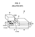
- FIG. 3 is an exploded perspective view showing a related art optical waveguide device disclosed in this patent.
- an optical waveguide device 50 includes an optical waveguide part 56, which consists of an optical waveguide forming layer 55 with lower cladding layers 521 and 522, a core layer 53, and an upper cladding layer 54 formed on a silicon substrate 51.
- the optical waveguide device 50 also includes a photonic device mounting part 57, which is configured by eliminating a part of the optical waveguide forming layer 55.
- a light emitting device 58 mounted on the photonic device mounting part 57 is optically connected to an end face of the optical waveguide part 56, which is exposed by the elimination of a part of the optical waveguide forming layer 55.
- the photonic device mounting part 57 includes a pedestal block 59, an alignment marker 60 consisting of a lower cladding layer 521, a pedestal block forming mask 62 consisting of a chromium (Cr) film 61 provided on the pedestal block 59, and the light emitting device 58 which contacts the mask 62.
- the lower cladding layers 521 and 522, the core layer 53, and the upper cladding layer 54 are atmospheric chemical vapor deposition (CVD) films.
- the optical waveguide device 50 is formed by surface-mounting the light emitting device 58 on a PLC chip with an optical waveguide circuit.
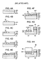
- FIG. 4 shows sectional views of a method of manufacturing the optical waveguide device of FIG. 3 , where the operations proceed in order of FIG. 4(a) to (h) .
- FIG. 4 shows sectional views of a method of manufacturing the optical waveguide device of FIG. 3 , where the operations proceed in order of FIG. 4(a) to (h) .
- the lower cladding layer 521 is deposited as a first layer on the silicon substrate 51.
- the chromium film 61 which later becomes a mask for forming the pedestal block, is patterned on the lower cladding layer 521.
- the chromium film 61 which becomes a mask for forming the alignment marker required for mounting the light emitting device 58, is patterned.
- the lower cladding layer 522 is deposited as a second layer.
- the core layer 53 which becomes a core of the optical waveguide part 56, is deposited on the lower cladding layer 522, and the waveguide is patterned by dry etching.
- an upper cladding layer 541 is deposited as the first layer for embedding the core layer 53 and reflow-processed at a high temperature.
- the upper cladding layer 541 consists of a low melting film.
- the temperature of the reflow process is generally between 800°C to 900°C.
- an upper cladding layer 542 is deposited as the second layer to complete a waveguide structure.
- a chromium film 63 and a photoresist film 64 are deposited, and are patterned so that only the chromium film 63 remains on the optical waveguide forming layer 55 as the optical waveguide part 56.
- the end face of the core layer 53 is exposed by dry etching by using the chromium film 63 as an etching mask.
- the pedestal block 59 and alignment marker 60 are formed by using the patterned chromium film 61 as an etching-stop mask 62 to complete the optical waveguide device.
- the height of the core layer 53 of the optical waveguide part 56 and the pedestal block 59 is only controlled by the accuracy of a film formation apparatus.
- the accuracy of the film formation apparatus is around 1%, due to variations in a wafer surface. Therefore, when the film thickness of the lower cladding layer 522 is 1.5 ⁇ m, a gap in height between the core layer 53 and the pedestal block 59 is only 15 nm.
- a heat treatment temperature of each individual operation is indicated.
- the film made by the plasma CVD can have a high refractive index, and so it is possible to increase a refractive index difference between a core and a cladding, to significantly improve the flexibility in design.
- a thin film formed by the plasma CVD requires a heat treatment at a high temperature, normally around 1,100°C.
- the core layer 53 is the atmospheric CVD film as previously described. This is because, if the core layer 53 is a plasma CVD film, the chromium film 61 is oxidized by the heat treatment at a high temperature, and the pedestal block forming mask 62 no longer functions correctly.
- Exemplary embodiments of the present invention overcome the above disadvantages and other disadvantages not described above. Also, the present invention is not required to overcome the disadvantages described above, and an exemplary embodiment of the present invention may not overcome any of the problems described above.
- An optical waveguide device is defined in claim 1, and a method of manufacturing an optical waveguide device according to the invention is defined in claim 2; claim 3 is related to a further development of the method of claim 2.
- the present invention provides an optical waveguide device which is capable of making a pedestal block with high accuracy, even when a heat treatment at a high temperature is required, and the manufacturing method thereof.
- an optical waveguide device which comprises an optical waveguide part and a photonic device mounting part.
- the optical waveguide part comprises an optical waveguide forming layer having a lower cladding layer, a core layer, and an upper cladding layer formed on a substrate.
- the photonic device mounting part is configured by eliminating a part of the optical waveguide forming layer.
- the photonic device mounted on the photonic device mounting part is optically connected to an end face of the optical waveguide part, which is exposed by the elimination of a part of the optical waveguide forming layer.
- the upper cladding layer comprising one layer or two or more layers.
- the photonic device mounting part comprises a pedestal block comprising at least one layer of the upper cladding layer provided on the substrate, and a mask consisting of a thin film provided on the pedestal block. The photonic device contacts the mask.
- the mask of the present invention is not an etching-stop mask to prevent etching below the upper cladding layer when etching the upper cladding.
- the mask of the present invention may form a part the pedestal block.
- the thin film which becomes the mask is provided on at least one layer constituting the upper cladding layer. Therefore, there is no influence on the thin film, even if the lower cladding layer and core layer undergo a heat treatment at a high temperature before forming the thin film. Therefore, it is possible to make the pedestal block with high accuracy even when a heat treatment at a high temperature is required.
- the material such as a silicon dioxide film (SiO 2 )
- height of the pedestal block are the same as those of at least one layer constituting the upper cladding layer.
- the lower cladding layer and the core layer may consist of a plasma CVD film.
- the plasma CVD film may be annealed after the film is formed at 1,000°C or higher, and preferably 1,100°C or higher.
- the refractive index of the core layer can be increased.
- the layers configuring the upper cladding layer may consist of deposited first and second layers.
- the photonic device mounting part has a pedestal block consisting of the second layer and a mask consisting of a thin film provided on the pedestal block.
- the lower cladding layer, the core layer and the first layer are eliminated.
- a method of manufacturing an optical waveguide device with an optical waveguide part and a photonic device mounting part comprises an optical waveguide forming layer having a lower cladding layer, a core layer, and an upper cladding layer formed on a substrate.
- the photonic device mounting part is formed by eliminating a part of the optical waveguide forming layer.
- the photonic device which is mounted on the photonic device mounting part is optically connected to an end face of the optical waveguide part, which is exposed by the elimination of a part of the optical waveguide forming layer.
- the method comprises the following operations.
- the first operation at least the lower cladding layer and the core layer are formed on the substrate.
- the second operation at least the lower cladding layer and the core layer are eliminated in a part to become the photonic device mounting part.
- at least one layer of the upper cladding layer is formed on a part to become the optical waveguide part and on a part to become the photonic device mounting part.
- a pedestal block layer consisting of at least one layer of the upper cladding layer is formed on the part to become the photonic device mounting part.
- a mask consisting of a thin film is formed on the pedestal block layer in the part to become the photonic device mounting part.
- a pedestal block is formed by eliminating the pedestal block layer other than under the mask by using the mask in the part to become the photonic device mounting part.
- the lower cladding layer and the core layer may be formed by a plasma CVD in the first operation.
- the method also includes an operation of annealing the lower cladding layer and the core layer at 1, 000°C or higher, and preferably 1,100°C or higher before the third operation.
- the upper cladding layer may consist of deposited first and second layers.
- the first operation the lower cladding layer and the core layer are deposited on the substrate by the plasma CVD, and the core is formed by dry etching, and then, the lower cladding layer and the core layer are annealed at 1, 000°C or over. And next, the first layer is formed on the core layer. In this case, the annealing may be performed after the film formation of the core layer which is after the film formation of the lower cladding layer.
- the second operation the lower cladding layer, the core layer and the first layer are eliminated in the part to become the photonic device mounting part.
- the second layer is formed on the part to become the optical waveguide part and on the part to become the photonic device mounting part. And a pedestal block layer consisting of the second layer is thereby formed on the part to become the photonic device mounting part.
- At least one of the upper cladding layers may consist of an atmospheric CVD film. Because there is no need to increase the refractive index of a cladding, it is possible to use atmospheric CVD film, for which the heat treatment temperature is relatively low, to avoid generation of wasteful thermal stress. Furthermore, this should preferably be a quartz film, such as a Boro-phospho silicate glass (BPSG) film with a low melting point and a dopant, such as boron orphosphorous. Using the BPSG film reduces the thermal stress and facilitates embedding of the core. It also improves flatness and thereby enables the pedestal block to be made with high accuracy.
- BPSG Boro-phospho silicate glass
- the second operation it is also possible to eliminate the lower cladding layer part of the way by reactive ion etching (RIE) and then eliminate the rest of the lower cladding layer by wet etching to the substrate.
- RIE reactive ion etching
- the lower cladding layer is the silicon dioxide film and the substrate is silicon
- a hydrofluoric acid mixture such as a buffered hydrofluoric acid.
- an optical waveguide device having a structure for matching height of a waveguide with the height of another optical device with high accuracy even when a high-temperature treatment is necessary.
- the pedestal block with high accuracy ,even after a necessary high-temperature treatment, by making the pedestal block with a low-melting silica film with a dopant such as boron or phosphorous, and utilizing the flatness due to its reflow characteristic.
- the upper cladding layer film doubles as the film to form the pedestal block.
- the thin film which becomes the mask for forming the pedestal block is provided on the upper cladding layer. Therefore, there is no influence on the thin film, even if the lower cladding layer and core layer undergo a heat treatment at a high temperature before forming the thin film. Therefore, it is possible to make the pedestal block with high accuracy even when a heat treatment at a high temperature is required.
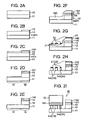
- FIG. 1 is an exploded perspective view showing an optical waveguide device according to an exemplary embodiment of the present invention.
- FIG. 1 shows that an optical waveguide device 10 comprises an optical waveguide part 16, which includes an optical waveguide forming layer 15 with lower cladding layer 12, a core layer 13, and an upper cladding layers 141 and 142 formed on a silicon substrate 11.
- the optical waveguide device 10 also includes a photonic device mounting part 17 formed by eliminating a part of the optical waveguide forming layer 15.
- a light emitting device 18, which is mounted on the photonic device mounting part 17, is optically connected to an end face of the optical waveguide part 16, which is exposed by the elimination of a part of the optical waveguide forming layer 15.
- the photonic device mounting part 17 includes a pedestal block 19, an alignment marker 20, and a mask 22.
- the pedestal block 19 and the alignment marker 20 consist of the upper cladding layer 142.
- the mask 22 comprises a chromium film 21 provided on the upper cladding layer 142.
- the light emitting device 18 contacts the mask 22.
- the photonic device mounting part 17 has a part where the upper cladding layer without the mask 22 thereon is eliminated and the surface of the silicon substrate 11 is exposed.
- the chromium film 21 which becomes the mask 22 is provided on the upper cladding layer 142. Therefore, there is no influence on the chromium film 21, even if the lower cladding layer 12 and core layer 13 undergo a heat treatment at a high temperature before forming the chromium film 21. Therefore, it is possible to make the pedestal block 19 with high accuracy even when a heat treatment at a high temperature is required.
- the lower cladding layers 12 and the core layer 13 consist of a plasma CVD film.
- the plasma CVD film is annealed at 1, 000°C or higher after the film formation. By using this film, it is possible to increase a refractive index difference between the core layer 13 and the lower cladding layer 12. Therefore, flexibility in designing an optical waveguide is significantly improved.
- FIG. 2 shows a method of manufacturing the optical waveguide device of FIG. 1 , where the operations proceed in order of FIG. 2(a) to (h) .
- FIG. 2 shows a method of manufacturing the optical waveguide device of FIG. 1 , where the operations proceed in order of FIG. 2(a) to (h) .
- the lower cladding layer 12 is formed on the silicon substrate 11 by a plasma CVD. If necessary, a high-temperature annealing process at about 1,100°C can be performed after the formation of the layer.
- a SiON film which becomes the core layer 13 is deposited on the lower cladding layer 12 by the plasma CVD, and the waveguide is patterned on the core layer 13 by dry etching. Thereafter, the high-temperature annealing process at about 1,100°C may be performed. The high-temperature annealing process may be performed before patterning the waveguide if the thermal stress is not problematic.
- a first upper cladding layer 141 is deposited for embedding the core layer 13.
- the first upper cladding layer 141 is then reflow-processed at about 850°C to embed the core layer 13.
- the first upper cladding layer 141 may be a low melting film, such as BPSG (Boro-phospho-silicate Glass) film deposited by an atmospheric pressure CVD.
- the lower cladding layer 12, the core layer 13 and the upper cladding layer 141 of the part for mounting the light emitting device 18 are etched part of the way through the lower cladding layer 12 by RIE (Reactive Ion Etching).
- the lower cladding layer 12 is etched by wet etching with a buffered hydrofluoric acid until the silicon substrate 11 becomes exposed.
- the reason for using the wet etching with the buffered hydrofluoric acid is to prevent the silicon substrate from being etched. While the RIE etches a small amount of the silicon, the buffered hydrofluoric acid does not etch the silicon. Therefore, it is possible to eliminate only the lower cladding layer 12 without eliminating the silicon substrate 11. Then, it is possible to form the pedestal block 19 with a highly accurate height.
- a second upper cladding layer 142 is deposited by an atmospheric pressure CVD.
- the second upper cladding layer 142 is then ref low-processed at about 850°C to improve the flatness of its surface.
- the second upper cladding layer 142 may be a low melting film, such as BPSG film.
- the chromium film 21 and a photoresist film 23 are deposited on the second upper cladding layer 142. Then, the mask 22 for forming the pedestal block 19 is patterned. In this case, the chromium film 21 which becomes the mask for forming the alignment marker required when mounting the light emitting device 18 is patterned at the same time. In addition, the chromium film 21 which becomes the mask for forming the end face of the core layer 13 is also patterned at the same time.
- an etching rate of the chromium film 21 should desirably be 1/10 or less of the etching rate of the second upper cladding layer 142.
- the chromium film is eliminated, and an insulating film, an electrode metal and the like are formed and patterned as required.
- the chromium film 21 on the optical waveguide part 16 is eliminated.
- the chromium film 21, which becomes the mask 22, is patterned after the high-temperature annealing process to form the pedestal block 19 and the alignment marker 20.
- relative accuracy of the height of the core layer 13 and the light emitting device 18 is decided by the accuracy of the film thickness of the lower cladding layer 12 formed by the plasma CVD and the accuracy of the film thickness of the upper cladding layer 142 formed by the atmospheric pressure CVD. Because the accuracy of the film thickness of both of them are 1 % or so, it is possible to keep variations at 2 % or so at the maximum. Therefore, an active layer 181 of the light emitting device 18 and the core layer 13 are optically connected with extremely high accuracy.
- FIG. 2 an example heat treatment temperature of each individual step is indicated.
- the verticality of an etching sidewall is improved. Also, the contact between the photoresist film and silicon dioxide film is improved via the chromium film. Further, it makes easier to recognize a marker by shielding infrared radiation. It is also possible to use a titanium film or the photoresist film instead of the chromium film 21.
Claims (3)
- Optische Wellenleitervorrichtung mit:einem optischen Wellenleiterteil (16) mit einer unteren Deckschicht (12), einer Kernschicht (13) und einer oberen Deckschicht undeinem Photonikvorrichtungs-Montageteil (17) mit einem Sockelblock (19), einer Maske (22) aus einem Dünnfilm, der auf dem Sockelblock (19) gebildet ist, und einer Photonikvorrichtung, die die Maske (22) kontaktiert,dadurch gekennzeichnet, dass die obere Deckschicht eine erste (141) und einer zweite (142) Schicht aufweist und dass der Sockelblock (19) aus der zweiten Schicht (142) besteht.
- Verfahren der Herstellung einer optischen Wellenleitervorrichtung mit:Ausbilden einer unteren Deckschicht auf einem Substrat durch chemische Plasmadampfzersetzung (CVD),Ausbilden einer Kernschicht auf der unteren Deckschicht durch Plasma-CVD,Tempern der unteren Deckschicht und der Kernschicht bei nicht weniger als 1.000°C,Ausbilden einer ersten Schicht als eine erste obere Deckschicht auf der Kernschicht,Entfernen der unteren Deckschicht, der Kernschicht und der ersten oberen Deckschicht in einem Photonikvorrichtungs-Montageteil (17),Ausbilden einer zweiten Schicht auf dem optischen Wellenleiterteil (16) als eine zweite obere Deckschicht und auf einem Photonikvorrichtungs-Montageteil (17) als eine Sockelblockschicht,Bilden einer Maske (22) aus einem Dünnfilm auf der Sockelblockschicht,Ausbilden eines Sockelblocks in dem Photonikvorrichtungs-Montageteil (17) durch Ätzen der Sockelblockschicht unter Verwendung der Maske als Ätzmaske.
- Verfahren der Herstellung einer optischen Wellenleitervorrichtung nach Anspruch 2,
wobei das Entfernen der unteren Deckschicht und der Kernschicht in dem Photonikvorrichtungs-Montageteil (17) durch erstens reaktives Ionenätzen und zweitens durch Nassätzen erfolgt.
Applications Claiming Priority (1)
| Application Number | Priority Date | Filing Date | Title |
|---|---|---|---|
| JP2006113349A JP4796884B2 (ja) | 2006-04-17 | 2006-04-17 | 光導波路デバイスの製造方法 |
Publications (3)
| Publication Number | Publication Date |
|---|---|
| EP1847860A2 EP1847860A2 (de) | 2007-10-24 |
| EP1847860A3 EP1847860A3 (de) | 2011-11-30 |
| EP1847860B1 true EP1847860B1 (de) | 2013-06-26 |
Family
ID=38328223
Family Applications (1)
| Application Number | Title | Priority Date | Filing Date |
|---|---|---|---|
| EP07007461.2A Active EP1847860B1 (de) | 2006-04-17 | 2007-04-11 | Optische Wellenleitervorrichtung mit optischem Baustein und Herstellungsverfahren dafür |
Country Status (5)
| Country | Link |
|---|---|
| US (2) | US7492984B2 (de) |
| EP (1) | EP1847860B1 (de) |
| JP (1) | JP4796884B2 (de) |
| CN (1) | CN101059586B (de) |
| TW (1) | TW200804883A (de) |
Families Citing this family (12)
| Publication number | Priority date | Publication date | Assignee | Title |
|---|---|---|---|---|
| JP2007298770A (ja) * | 2006-04-28 | 2007-11-15 | Nec Corp | 光導波路デバイス及びその製造方法 |
| JP5186785B2 (ja) * | 2007-03-23 | 2013-04-24 | 日本電気株式会社 | 光導波路デバイス、光導波路デバイス用光素子実装システム、光素子実装方法、及びそのプログラム |
| JP5229617B2 (ja) * | 2008-07-11 | 2013-07-03 | 日本電気株式会社 | 光導波路デバイスとその製造方法 |
| CN102356337B (zh) * | 2009-03-17 | 2014-03-12 | 日本电气株式会社 | 光波导装置及其制造方法 |
| KR101199302B1 (ko) * | 2009-10-13 | 2012-11-09 | 한국전자통신연구원 | 광 소자 및 그 제조 방법 |
| US10009106B2 (en) * | 2012-05-14 | 2018-06-26 | Acacia Communications, Inc. | Silicon photonics multicarrier optical transceiver |
| US9217836B2 (en) * | 2012-10-23 | 2015-12-22 | Kotura, Inc. | Edge coupling of optical devices |
| TWI565985B (zh) * | 2012-12-14 | 2017-01-11 | 鴻海精密工業股份有限公司 | 脊型光波導的製造方法 |
| JP6286853B2 (ja) * | 2013-04-04 | 2018-03-07 | 富士通株式会社 | 電子装置とその製造方法、及び電子機器 |
| US9099145B1 (en) * | 2013-12-24 | 2015-08-04 | Western Digital (Fremont), Llc | High contrast alignment marker |
| KR102604742B1 (ko) | 2015-12-23 | 2023-11-22 | 삼성전자주식회사 | 광 소자 및 그 제조 방법 |
| JP6820671B2 (ja) | 2016-06-02 | 2021-01-27 | 富士通株式会社 | 光回路デバイスとこれを用いた光トランシーバ |
Family Cites Families (13)
| Publication number | Priority date | Publication date | Assignee | Title |
|---|---|---|---|---|
| JP3117107B2 (ja) * | 1993-08-03 | 2000-12-11 | シャープ株式会社 | 光集積回路素子の組立構造 |
| JPH09145965A (ja) * | 1995-11-22 | 1997-06-06 | Hitachi Ltd | 光モジュール及びその製造方法 |
| JP2823044B2 (ja) * | 1996-05-14 | 1998-11-11 | 日本電気株式会社 | 光結合回路及びその製造方法 |
| JP2000075153A (ja) * | 1998-08-31 | 2000-03-14 | Fujitsu Ltd | 光学部品付基板及び光学装置の製造方法 |
| JP2000098157A (ja) * | 1998-09-25 | 2000-04-07 | Japan Aviation Electronics Industry Ltd | 光分岐装置およびその製造方法 |
| CN1183396C (zh) * | 1999-07-16 | 2005-01-05 | 混合微技术有限公司 | 形成组装和对准光电子器件和光波导的组件结构的方法 |
| JP3698601B2 (ja) * | 1999-10-08 | 2005-09-21 | 日本電信電話株式会社 | 光モジュール |
| KR100442609B1 (ko) * | 2002-03-05 | 2004-08-02 | 삼성전자주식회사 | 플립칩 본딩구조 및 본딩방법 |
| KR100456672B1 (ko) * | 2002-03-30 | 2004-11-10 | 한국전자통신연구원 | 광도파로 플랫폼 및 그 제조 방법 |
| KR100427582B1 (ko) * | 2002-08-08 | 2004-04-28 | 한국전자통신연구원 | 광도파로 플랫폼 및 그 제조 방법 |
| JP2004294655A (ja) * | 2003-03-26 | 2004-10-21 | Nec Corp | 光導波路の製造方法 |
| CN1690747A (zh) * | 2004-04-20 | 2005-11-02 | 中国科学院半导体研究所 | 光纤定位槽、光斑转换器和光波导器件的一体化制作方法 |
| JP2007298770A (ja) * | 2006-04-28 | 2007-11-15 | Nec Corp | 光導波路デバイス及びその製造方法 |
-
2006
- 2006-04-17 JP JP2006113349A patent/JP4796884B2/ja not_active Expired - Fee Related
-
2007
- 2007-04-03 TW TW096111742A patent/TW200804883A/zh unknown
- 2007-04-09 US US11/733,044 patent/US7492984B2/en not_active Expired - Fee Related
- 2007-04-11 EP EP07007461.2A patent/EP1847860B1/de active Active
- 2007-04-12 CN CN2007100904839A patent/CN101059586B/zh not_active Expired - Fee Related
-
2009
- 2009-01-02 US US12/348,205 patent/US7778504B2/en active Active
Also Published As
| Publication number | Publication date |
|---|---|
| US7778504B2 (en) | 2010-08-17 |
| CN101059586A (zh) | 2007-10-24 |
| EP1847860A3 (de) | 2011-11-30 |
| JP4796884B2 (ja) | 2011-10-19 |
| US7492984B2 (en) | 2009-02-17 |
| US20070274653A1 (en) | 2007-11-29 |
| TW200804883A (en) | 2008-01-16 |
| CN101059586B (zh) | 2010-04-07 |
| EP1847860A2 (de) | 2007-10-24 |
| JP2007286340A (ja) | 2007-11-01 |
| US20090116803A1 (en) | 2009-05-07 |
Similar Documents
| Publication | Publication Date | Title |
|---|---|---|
| EP1847860B1 (de) | Optische Wellenleitervorrichtung mit optischem Baustein und Herstellungsverfahren dafür | |
| US8594477B2 (en) | Optical waveguide device and method of manufacturing thereof | |
| US7361520B2 (en) | Optical waveguide device and manufacturing method thereof | |
| US7323352B2 (en) | Process for making light waveguide element | |
| US5299276A (en) | Waveguide type optical device and method for manufacturing the same | |
| JP5229617B2 (ja) | 光導波路デバイスとその製造方法 | |
| EP0905533B1 (de) | Optische Anordnung und ihr Herstellungsverfahren | |
| CN101398512A (zh) | 平面光波线路及其制作方法和光波导装置 | |
| US6804444B2 (en) | Optical waveguide platform and manufacturing method thereof | |
| KR20040013694A (ko) | 광도파로 플랫폼 및 그 제조 방법 | |
| EP1211532A2 (de) | Optische Vorrichtung zur Montage optischer Elemente | |
| EP0762162A1 (de) | Eine Faser-planarer Wellenleiterkopplung enthaltende Vorrichtung und ihr Herstellungsverfahren | |
| US6631235B1 (en) | Planar lightwave circuit platform and method for manufacturing the same | |
| JPH11190811A (ja) | 光デバイス実装用基板及びその製造方法並びに光モジュール | |
| WO2005066677A2 (en) | Improved accuracy fiducial marks for trench implementation in optical transceiver platforms | |
| WO2003034115A2 (en) | Coupling a semiconducter laser to an optical waveguide | |
| JPH08304671A (ja) | 光送受信器及びその製造方法 | |
| KR20030056333A (ko) | 광도파로 플랫폼 및 그 제조 방법 |
Legal Events
| Date | Code | Title | Description |
|---|---|---|---|
| PUAI | Public reference made under article 153(3) epc to a published international application that has entered the european phase |
Free format text: ORIGINAL CODE: 0009012 |
|
| AK | Designated contracting states |
Kind code of ref document: A2 Designated state(s): AT BE BG CH CY CZ DE DK EE ES FI FR GB GR HU IE IS IT LI LT LU LV MC MT NL PL PT RO SE SI SK TR |
|
| AX | Request for extension of the european patent |
Extension state: AL BA HR MK YU |
|
| PUAL | Search report despatched |
Free format text: ORIGINAL CODE: 0009013 |
|
| AK | Designated contracting states |
Kind code of ref document: A3 Designated state(s): AT BE BG CH CY CZ DE DK EE ES FI FR GB GR HU IE IS IT LI LT LU LV MC MT NL PL PT RO SE SI SK TR |
|
| AX | Request for extension of the european patent |
Extension state: AL BA HR MK RS |
|
| RIC1 | Information provided on ipc code assigned before grant |
Ipc: G02B 6/42 20060101ALI20111025BHEP Ipc: G02B 6/12 20060101AFI20111025BHEP |
|
| 17P | Request for examination filed |
Effective date: 20120530 |
|
| AKX | Designation fees paid |
Designated state(s): DE FR IT |
|
| GRAP | Despatch of communication of intention to grant a patent |
Free format text: ORIGINAL CODE: EPIDOSNIGR1 |
|
| GRAS | Grant fee paid |
Free format text: ORIGINAL CODE: EPIDOSNIGR3 |
|
| GRAA | (expected) grant |
Free format text: ORIGINAL CODE: 0009210 |
|
| AK | Designated contracting states |
Kind code of ref document: B1 Designated state(s): DE FR IT |
|
| REG | Reference to a national code |
Ref country code: DE Ref legal event code: R096 Ref document number: 602007031222 Country of ref document: DE Effective date: 20130822 |
|
| PLBE | No opposition filed within time limit |
Free format text: ORIGINAL CODE: 0009261 |
|
| STAA | Information on the status of an ep patent application or granted ep patent |
Free format text: STATUS: NO OPPOSITION FILED WITHIN TIME LIMIT |
|
| 26N | No opposition filed |
Effective date: 20140327 |
|
| REG | Reference to a national code |
Ref country code: DE Ref legal event code: R097 Ref document number: 602007031222 Country of ref document: DE Effective date: 20140327 |
|
| REG | Reference to a national code |
Ref country code: DE Ref legal event code: R119 Ref document number: 602007031222 Country of ref document: DE |
|
| REG | Reference to a national code |
Ref country code: DE Ref legal event code: R119 Ref document number: 602007031222 Country of ref document: DE Effective date: 20141101 |
|
| REG | Reference to a national code |
Ref country code: FR Ref legal event code: ST Effective date: 20141231 |
|
| PG25 | Lapsed in a contracting state [announced via postgrant information from national office to epo] |
Ref country code: DE Free format text: LAPSE BECAUSE OF NON-PAYMENT OF DUE FEES Effective date: 20141101 |
|
| PG25 | Lapsed in a contracting state [announced via postgrant information from national office to epo] |
Ref country code: FR Free format text: LAPSE BECAUSE OF NON-PAYMENT OF DUE FEES Effective date: 20140430 |