EP1844492B1 - Non-volatile nanocrystal memory and method therefor - Google Patents
Non-volatile nanocrystal memory and method therefor Download PDFInfo
- Publication number
- EP1844492B1 EP1844492B1 EP05854006A EP05854006A EP1844492B1 EP 1844492 B1 EP1844492 B1 EP 1844492B1 EP 05854006 A EP05854006 A EP 05854006A EP 05854006 A EP05854006 A EP 05854006A EP 1844492 B1 EP1844492 B1 EP 1844492B1
- Authority
- EP
- European Patent Office
- Prior art keywords
- insulating layer
- forming
- nitrogen content
- nanocrystals
- layer
- Prior art date
- Legal status (The legal status is an assumption and is not a legal conclusion. Google has not performed a legal analysis and makes no representation as to the accuracy of the status listed.)
- Expired - Lifetime
Links
Images

Classifications
-
- H—ELECTRICITY
- H10—SEMICONDUCTOR DEVICES; ELECTRIC SOLID-STATE DEVICES NOT OTHERWISE PROVIDED FOR
- H10D—INORGANIC ELECTRIC SEMICONDUCTOR DEVICES
- H10D30/00—Field-effect transistors [FET]
- H10D30/60—Insulated-gate field-effect transistors [IGFET]
- H10D30/69—IGFETs having charge trapping gate insulators, e.g. MNOS transistors
- H10D30/694—IGFETs having charge trapping gate insulators, e.g. MNOS transistors characterised by the shapes, relative sizes or dispositions of the gate electrodes
- H10D30/697—IGFETs having charge trapping gate insulators, e.g. MNOS transistors characterised by the shapes, relative sizes or dispositions of the gate electrodes having trapping at multiple separated sites, e.g. multi-particles trapping sites
-
- H—ELECTRICITY
- H10—SEMICONDUCTOR DEVICES; ELECTRIC SOLID-STATE DEVICES NOT OTHERWISE PROVIDED FOR
- H10P—GENERIC PROCESSES OR APPARATUS FOR THE MANUFACTURE OR TREATMENT OF DEVICES COVERED BY CLASS H10
- H10P10/00—Bonding of wafers, substrates or parts of devices
-
- B—PERFORMING OPERATIONS; TRANSPORTING
- B82—NANOTECHNOLOGY
- B82Y—SPECIFIC USES OR APPLICATIONS OF NANOSTRUCTURES; MEASUREMENT OR ANALYSIS OF NANOSTRUCTURES; MANUFACTURE OR TREATMENT OF NANOSTRUCTURES
- B82Y10/00—Nanotechnology for information processing, storage or transmission, e.g. quantum computing or single electron logic
-
- H—ELECTRICITY
- H10—SEMICONDUCTOR DEVICES; ELECTRIC SOLID-STATE DEVICES NOT OTHERWISE PROVIDED FOR
- H10D—INORGANIC ELECTRIC SEMICONDUCTOR DEVICES
- H10D30/00—Field-effect transistors [FET]
- H10D30/60—Insulated-gate field-effect transistors [IGFET]
- H10D30/68—Floating-gate IGFETs
- H10D30/6891—Floating-gate IGFETs characterised by the shapes, relative sizes or dispositions of the floating gate electrode
- H10D30/6893—Floating-gate IGFETs characterised by the shapes, relative sizes or dispositions of the floating gate electrode wherein the floating gate has multiple non-connected parts, e.g. multi-particle floating gate
-
- H—ELECTRICITY
- H10—SEMICONDUCTOR DEVICES; ELECTRIC SOLID-STATE DEVICES NOT OTHERWISE PROVIDED FOR
- H10D—INORGANIC ELECTRIC SEMICONDUCTOR DEVICES
- H10D64/00—Electrodes of devices having potential barriers
- H10D64/01—Manufacture or treatment
- H10D64/031—Manufacture or treatment of data-storage electrodes
- H10D64/035—Manufacture or treatment of data-storage electrodes comprising conductor-insulator-conductor-insulator-semiconductor structures
-
- H—ELECTRICITY
- H10—SEMICONDUCTOR DEVICES; ELECTRIC SOLID-STATE DEVICES NOT OTHERWISE PROVIDED FOR
- H10D—INORGANIC ELECTRIC SEMICONDUCTOR DEVICES
- H10D64/00—Electrodes of devices having potential barriers
- H10D64/60—Electrodes characterised by their materials
- H10D64/66—Electrodes having a conductor capacitively coupled to a semiconductor by an insulator, e.g. MIS electrodes
- H10D64/68—Electrodes having a conductor capacitively coupled to a semiconductor by an insulator, e.g. MIS electrodes characterised by the insulator, e.g. by the gate insulator
- H10D64/681—Electrodes having a conductor capacitively coupled to a semiconductor by an insulator, e.g. MIS electrodes characterised by the insulator, e.g. by the gate insulator having a compositional variation, e.g. multilayered
- H10D64/685—Electrodes having a conductor capacitively coupled to a semiconductor by an insulator, e.g. MIS electrodes characterised by the insulator, e.g. by the gate insulator having a compositional variation, e.g. multilayered being perpendicular to the channel plane
-
- H—ELECTRICITY
- H10—SEMICONDUCTOR DEVICES; ELECTRIC SOLID-STATE DEVICES NOT OTHERWISE PROVIDED FOR
- H10D—INORGANIC ELECTRIC SEMICONDUCTOR DEVICES
- H10D64/00—Electrodes of devices having potential barriers
- H10D64/60—Electrodes characterised by their materials
- H10D64/66—Electrodes having a conductor capacitively coupled to a semiconductor by an insulator, e.g. MIS electrodes
- H10D64/68—Electrodes having a conductor capacitively coupled to a semiconductor by an insulator, e.g. MIS electrodes characterised by the insulator, e.g. by the gate insulator
- H10D64/693—Electrodes having a conductor capacitively coupled to a semiconductor by an insulator, e.g. MIS electrodes characterised by the insulator, e.g. by the gate insulator the insulator comprising nitrogen, e.g. nitrides, oxynitrides or nitrogen-doped materials
Definitions
- the present invention relates to non-volatile memories having nanocrystals for storage, and more particularly to the insulation of and over such nanocrystals.
- Nanocrystal memories have been found to be advantageous over floating gate memories due to increased immunity to charge leakage through gate dielectric defects.
- One issue in nanocrystal memories is the potential for electron trapping in the dielectric stack under the control gate. This problem occurs during hot carrier injection of electrons into the nanocrystals. A fraction of the electrons not trapped by the nanocrystals can be trapped in the dielectric stack, which leads to a shift in the threshold voltage. These electrons trapped in the dielectric stack are not electrically erasable so they accumulate with repeated program and erase cycles. Thus the shift in threshold voltage continues to grow with the repeated program erase operations and requires circuit designs that attempt to mitigate this effect. In addition to this, dielectric trapped charge can lead to degradation in reliability due to internal electric fields working concomitantly with external bias.
- electrons trapped in the portion of the dielectric stack between the control gate and the nanocrystals can degrade data retention of nanocrystals programmed with electrons by accelerating tunneling loss through the portion of the dielectric stack between the nanocrystals and the substrate.
- Hybrid silicon nanocrystal silicon nitride Dynamic Random Access Memory discloses a hybrid Si-NC/SiN non volatile memory wherein a SiN layer is CVD-deposited on top of the Si-NC. Charges are stored in Si-NC or SiN charge trapping layer or both ( IEEE Transactions on nanotechnology, vol.2, n°4, p.335-340, 1 Dec. 2003 ).
- a nanocrystal non-volatile memory has a dielectric between the control gate and the nanocrystals that has a nitrogen content sufficient to reduce the locations in the dielectric where electrons can be trapped. This is achieved by grading the nitrogen concentration. The concentration of nitrogen is highest near the nanocrystals where the concentration of electron/hole traps tend to be the highest and is reduced toward the control gate where the concentration of electron/hole traps is lower. This has been found to have the beneficial effect of reducing the number of locations where charge can be trapped. This is better understood with reference to the drawings and the following description.
- FIG. 1 Shown in FIG. 1 is a semiconductor device 10 comprising a substrate 12, a gate dielectric 14 over substrate 12, a plurality of nanocrystals 16 over the gate dielectric 14.
- Substrate 12 is preferably a bulk silicon substrate but could be an SOI substrate also and could be a different semiconductor material than silicon.
- Gate dielectric layer 14 is preferably a grown oxide that is 50 to 100 Angstroms in thickness and has a graded nitrogen content which is highest farthest from nanocrystals 16 and closest to substrate 12.
- Nanocrystals 16 in this example are made of silicon and have a density of between five times ten to the eleventh (5e11) and 1.2e12 per centimeter squared. Nanocrystals 16 vary in size between about 3 to 10 nanometers.
- Nanocrystals 16 are preferably deposited by chemical deposition, but other processes may also be used. Other processes for forming nanocrystals include recrystallization of a thin amorphous layer of silicon and the deposition of prefabricated nanocrystals. Subsequent to nanocrystal formation, nanocrystals 16 may be passivated by oxidizing them using nitrous oxide.
- semiconductor device 10 after forming a nitride-doped oxide layer 18 over and around nanocrystals 16. It is preferably about 3 to five nanometers in thickness and forms a first portion of a dielectric between the nanocrystals and a control gate that is not yet formed.
- the nitrogen content in layer 18 is graded. The highest nitrogen content is closest to the nanocrystals and begins at about 5-10 atomic percent. The nitrogen content is reduced away from nanocrystals 16 to eventually less than about 2 atomic percent.
- This grading is preferably achieved by reacting small amounts of ammonia with oxide forming gases such as dichlorosilane and nitrous oxide and gradually decreasing the flow rate of the ammonia.
- An alternative is to implant nitrogen into an oxide layer in a series of implant steps.
- the heaviest dose implant is with the highest energy and the lightest dose implant is with the lowest energy.
- This implantation is preferably performed in a remote plasma environment to prevent damage to layer 18.
- the nitrogen in the oxide layer during subsequent annealing steps saturates dangling bonds in the originally formed oxide layer.
- silicon-hydrogen bonds that have weak immunity to hot electrons are converted to more robust silicon-nitrogen bonds. Since the highest concentration of such bond defects is at the interface between dielectric layers, in this case between layers 14 and 18, and between the nanocrystals 16 and dielectric layer 18, a higher concentration of nitrogen is needed in these interface regions. Further away from the interface, the bond defects are fewer and require less nitrogen. Excessive nitrogen in these areas is deleterious to the memory device by acting as electron/hole traps. Additionally, oxygen can be implanted into layer 18 to aid in densification.
- Dielectric layer 20 is preferably silicon oxide and deposited by reacting a silicon-containing precursor such as silane or dichlorosilane with an oxidizer such as oxygen or nitrous oxide in a chemical vapor deposition chamber at between about 500 and 900 degrees Celsius. Layer 20 is typically between four and ten nanometers in thickness.
- FIG. 4 Shown in FIG. 4 is semiconductor device 10 after performing remote plasma nitridation of layer 20 to form a nitrided layer 22.
- the nitrogen content in nitrided layer 22 is preferably less than about 2 atomic percent. Since achieving such small nitrogen content is difficult by CVD, remote plasma deposition is the preferred approach.
- the energy of the remote plasma can be reduced over time in conjunction with a reduction in the flow of the nitrogen-containing species in order to achieve a graded nitrogen concentration in nitrided layer 22.
- the higher nitrogen concentration in such case is at the interface of layers 18 and 22 and the lower concentration is at the top surface of layer 22.
- Implanting nitrogen is also an alternative but remote plasma is preferable due to there being less damage at and near the surface of layer 20 compared to implanting.
- This remote plasma deposition, with enough energy, can also be utilized to introduce additional nitrogen into layer 18. Additionally, oxygen can be implanted into layer 20 to aid in densification.
- annealing steps are performed, preferably at about greater than 700 degrees Celsius or higher.
- a first of these annealing steps is done in an inert ambient such as nitrogen or argon at about greater than 800 degrees Celsius. This step facilitates nitrogen bonding and expels free hydrogen from layers 18 and 22.
- a second of these annealing steps is in a dilute oxidizing ambient and is for removing non-stoichiometric defects that may still be present.
- a third of these annealing steps is performed close to or about the glass transition temperature, which is about 950 degrees Celsius. The high degree of atomic motion during this reflow condition facilitates the structure to relax the stress of layers 18 and 22.
- the second and third annealing steps may be able to be combined into a single annealing step.
- the annealing temperature preferably does not exceed 1100 degrees Celsius.
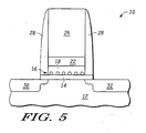
- FIG. 5 Shown in FIG. 5 is semiconductor device 10 after performing known steps to form an NVM device comprising a control gate 26, a sidewall spacer 28 around control gate 26, a source/drain region 30 on one side of control gate 26 and in substrate 12, and a source/drain region 32 on the other side of control gate 26 and in substrate 12.
- the resulting semiconductor device 10 of FIG. 5 is a transistor useful as the NVM device and for forming arrays of such devices.
- Layers 18 and 22 with their nitrogen content as described reduces threshold shift due to electron/hole trapping.
- Another benefit of the described approach is that layers 18 and 22 have increased density. Unlike thermally grown oxide such as layer 14, deposited oxides are less dense and stoichiometrically imperfect.
- the gate dielectric layer 14 was described as grown oxide but could instead be a deposited high k dielectric. Accordingly, the specification and figures are to be regarded in an illustrative rather than a restrictive sense, and all such modifications are intended to be included within the scope of present invention.
Landscapes
- Engineering & Computer Science (AREA)
- Chemical & Material Sciences (AREA)
- Nanotechnology (AREA)
- Physics & Mathematics (AREA)
- Mathematical Physics (AREA)
- Theoretical Computer Science (AREA)
- Crystallography & Structural Chemistry (AREA)
- Semiconductor Memories (AREA)
- Non-Volatile Memory (AREA)
- Formation Of Insulating Films (AREA)
- Physical Or Chemical Processes And Apparatus (AREA)
- Carbon And Carbon Compounds (AREA)
Applications Claiming Priority (2)
| Application Number | Priority Date | Filing Date | Title |
|---|---|---|---|
| US11/043,826 US7361567B2 (en) | 2005-01-26 | 2005-01-26 | Non-volatile nanocrystal memory and method therefor |
| PCT/US2005/045207 WO2006080999A2 (en) | 2005-01-26 | 2005-12-14 | Non-volatile nanocrystal memory and method therefor |
Publications (3)
| Publication Number | Publication Date |
|---|---|
| EP1844492A2 EP1844492A2 (en) | 2007-10-17 |
| EP1844492A4 EP1844492A4 (en) | 2009-10-21 |
| EP1844492B1 true EP1844492B1 (en) | 2010-07-07 |
Family
ID=36697390
Family Applications (1)
| Application Number | Title | Priority Date | Filing Date |
|---|---|---|---|
| EP05854006A Expired - Lifetime EP1844492B1 (en) | 2005-01-26 | 2005-12-14 | Non-volatile nanocrystal memory and method therefor |
Country Status (9)
| Country | Link |
|---|---|
| US (1) | US7361567B2 (enExample) |
| EP (1) | EP1844492B1 (enExample) |
| JP (1) | JP4980931B2 (enExample) |
| KR (1) | KR101219067B1 (enExample) |
| CN (1) | CN101438392A (enExample) |
| AT (1) | ATE473515T1 (enExample) |
| DE (1) | DE602005022229D1 (enExample) |
| TW (1) | TWI407492B (enExample) |
| WO (1) | WO2006080999A2 (enExample) |
Families Citing this family (25)
| Publication number | Priority date | Publication date | Assignee | Title |
|---|---|---|---|---|
| KR100673205B1 (ko) * | 2004-11-24 | 2007-01-22 | 주식회사 하이닉스반도체 | 플래쉬 메모리소자의 제조방법 |
| US20060166435A1 (en) * | 2005-01-21 | 2006-07-27 | Teo Lee W | Synthesis of GE nanocrystal memory cell and using a block layer to control oxidation kinetics |
| US7338894B2 (en) * | 2005-01-26 | 2008-03-04 | Freescale Semiconductor, Inc. | Semiconductor device having nitridated oxide layer and method therefor |
| JP2007036025A (ja) * | 2005-07-28 | 2007-02-08 | Nec Electronics Corp | 不揮発性メモリ半導体装置およびその製造方法 |
| US7525149B2 (en) * | 2005-08-24 | 2009-04-28 | Micron Technology, Inc. | Combined volatile and non-volatile memory device with graded composition insulator stack |
| TWI289336B (en) * | 2005-11-07 | 2007-11-01 | Ind Tech Res Inst | Nanocrystal memory component, manufacturing method thereof and memory comprising the same |
| US7767588B2 (en) * | 2006-02-28 | 2010-08-03 | Freescale Semiconductor, Inc. | Method for forming a deposited oxide layer |
| US7773493B2 (en) * | 2006-09-29 | 2010-08-10 | Intel Corporation | Probe-based storage device |
| US20080150004A1 (en) * | 2006-12-20 | 2008-06-26 | Nanosys, Inc. | Electron Blocking Layers for Electronic Devices |
| US7847341B2 (en) | 2006-12-20 | 2010-12-07 | Nanosys, Inc. | Electron blocking layers for electronic devices |
| US8686490B2 (en) * | 2006-12-20 | 2014-04-01 | Sandisk Corporation | Electron blocking layers for electronic devices |
| US20080150009A1 (en) * | 2006-12-20 | 2008-06-26 | Nanosys, Inc. | Electron Blocking Layers for Electronic Devices |
| US7846793B2 (en) * | 2007-10-03 | 2010-12-07 | Applied Materials, Inc. | Plasma surface treatment for SI and metal nanocrystal nucleation |
| US7871886B2 (en) * | 2008-12-19 | 2011-01-18 | Freescale Semiconductor, Inc. | Nanocrystal memory with differential energy bands and method of formation |
| US7799634B2 (en) * | 2008-12-19 | 2010-09-21 | Freescale Semiconductor, Inc. | Method of forming nanocrystals |
| US8021970B2 (en) * | 2009-03-20 | 2011-09-20 | Freescale Semiconductor, Inc. | Method of annealing a dielectric layer |
| JP6125846B2 (ja) * | 2012-03-22 | 2017-05-10 | 株式会社日立国際電気 | 半導体装置の製造方法、基板処理方法、基板処理装置およびプログラム |
| CN102709330B (zh) * | 2012-05-22 | 2016-04-27 | 上海华力微电子有限公司 | 一种具有低操作电压的be-sonos结构器件及形成方法 |
| CN102709315A (zh) * | 2012-05-22 | 2012-10-03 | 上海华力微电子有限公司 | 一种具有锥形能带的be-sonos结构器件及形成方法 |
| US8994006B2 (en) * | 2012-10-02 | 2015-03-31 | International Business Machines Corporation | Non-volatile memory device employing semiconductor nanoparticles |
| US8895397B1 (en) | 2013-10-15 | 2014-11-25 | Globalfoundries Singapore Pte. Ltd. | Methods for forming thin film storage memory cells |
| US9171858B2 (en) | 2013-12-30 | 2015-10-27 | Globalfoundries Singapore Pte. Ltd. | Multi-level memory cells and methods for forming multi-level memory cells |
| US9953841B2 (en) * | 2015-05-08 | 2018-04-24 | Macronix International Co., Ltd. | Semiconductor device and method of fabricating the same |
| US11756832B2 (en) * | 2019-09-30 | 2023-09-12 | Taiwan Semiconductor Manufacturing Company, Ltd. | Gate structures in semiconductor devices |
| DE102020100099B4 (de) * | 2019-09-30 | 2025-09-11 | Taiwan Semiconductor Manufacturing Co., Ltd. | Gatestrukturen in halbleitervorrichtungen und deren herstellung |
Family Cites Families (12)
| Publication number | Priority date | Publication date | Assignee | Title |
|---|---|---|---|---|
| US6320784B1 (en) * | 2000-03-14 | 2001-11-20 | Motorola, Inc. | Memory cell and method for programming thereof |
| US6413819B1 (en) * | 2000-06-16 | 2002-07-02 | Motorola, Inc. | Memory device and method for using prefabricated isolated storage elements |
| AU2001263370A1 (en) * | 2000-06-16 | 2002-01-02 | Motorola, Inc. | Memory device including nanoclusters and method for manufacture |
| US6297095B1 (en) * | 2000-06-16 | 2001-10-02 | Motorola, Inc. | Memory device that includes passivated nanoclusters and method for manufacture |
| TW525263B (en) * | 2000-09-28 | 2003-03-21 | Chartered Semiconductor Mfg | Formation of interfacial oxide layer at the Si3N4/Si interface by H2/O2 annealing |
| US6444545B1 (en) * | 2000-12-19 | 2002-09-03 | Motorola, Inc. | Device structure for storing charge and method therefore |
| JP2002261175A (ja) | 2000-12-28 | 2002-09-13 | Sony Corp | 不揮発性半導体記憶装置およびその製造方法 |
| JP2002231834A (ja) | 2001-02-02 | 2002-08-16 | Ricoh Co Ltd | 半導体記憶装置 |
| US6713127B2 (en) * | 2001-12-28 | 2004-03-30 | Applied Materials, Inc. | Methods for silicon oxide and oxynitride deposition using single wafer low pressure CVD |
| TW569377B (en) * | 2002-03-20 | 2004-01-01 | Taiwan Semiconductor Mfg | Improvement method for thickness uniformity of super-thin nitridation gate dielectric |
| JP2004207613A (ja) * | 2002-12-26 | 2004-07-22 | Matsushita Electric Ind Co Ltd | 半導体装置及びその製造方法 |
| US7338894B2 (en) * | 2005-01-26 | 2008-03-04 | Freescale Semiconductor, Inc. | Semiconductor device having nitridated oxide layer and method therefor |
-
2005
- 2005-01-26 US US11/043,826 patent/US7361567B2/en not_active Expired - Fee Related
- 2005-12-14 DE DE602005022229T patent/DE602005022229D1/de not_active Expired - Lifetime
- 2005-12-14 AT AT05854006T patent/ATE473515T1/de not_active IP Right Cessation
- 2005-12-14 JP JP2007552129A patent/JP4980931B2/ja not_active Expired - Fee Related
- 2005-12-14 CN CNA2005800409629A patent/CN101438392A/zh active Pending
- 2005-12-14 KR KR1020077017264A patent/KR101219067B1/ko not_active Expired - Fee Related
- 2005-12-14 EP EP05854006A patent/EP1844492B1/en not_active Expired - Lifetime
- 2005-12-14 WO PCT/US2005/045207 patent/WO2006080999A2/en not_active Ceased
-
2006
- 2006-01-04 TW TW095100396A patent/TWI407492B/zh active
Also Published As
| Publication number | Publication date |
|---|---|
| JP4980931B2 (ja) | 2012-07-18 |
| KR20070099625A (ko) | 2007-10-09 |
| KR101219067B1 (ko) | 2013-01-18 |
| EP1844492A2 (en) | 2007-10-17 |
| CN101438392A (zh) | 2009-05-20 |
| EP1844492A4 (en) | 2009-10-21 |
| US20060166452A1 (en) | 2006-07-27 |
| ATE473515T1 (de) | 2010-07-15 |
| DE602005022229D1 (de) | 2010-08-19 |
| US7361567B2 (en) | 2008-04-22 |
| TWI407492B (zh) | 2013-09-01 |
| WO2006080999A2 (en) | 2006-08-03 |
| JP2008532260A (ja) | 2008-08-14 |
| TW200629383A (en) | 2006-08-16 |
| WO2006080999A3 (en) | 2009-04-23 |
Similar Documents
| Publication | Publication Date | Title |
|---|---|---|
| EP1844492B1 (en) | Non-volatile nanocrystal memory and method therefor | |
| US6949433B1 (en) | Method of formation of semiconductor resistant to hot carrier injection stress | |
| US10790364B2 (en) | SONOS stack with split nitride memory layer | |
| US6740605B1 (en) | Process for reducing hydrogen contamination in dielectric materials in memory devices | |
| KR100894098B1 (ko) | 빠른 소거속도 및 향상된 리텐션 특성을 갖는 불휘발성메모리소자 및 그 제조방법 | |
| US7419888B2 (en) | Method of forming a silicon-rich nanocrystalline structure by an atomic layer deposition process and method of manufacturing a non-volatile semiconductor device using the same | |
| US9349824B2 (en) | Oxide-nitride-oxide stack having multiple oxynitride layers | |
| CN100447953C (zh) | 于二位eeprom装置制造ono浮动栅极的高温氧化物沉淀方法 | |
| US6458677B1 (en) | Process for fabricating an ONO structure | |
| US20070120179A1 (en) | SONOS type non-volatile memory devices having a laminate blocking insulation layer and methods of manufacturing the same | |
| CN101517714A (zh) | Sonos ono堆栈等比缩小 | |
| US6958511B1 (en) | Flash memory device and method of fabrication thereof including a bottom oxide layer with two regions with different concentrations of nitrogen | |
| US20100029091A1 (en) | Method of Forming Tunnel Insulation Layer in Flash Memory Device | |
| USRE31083E (en) | Non-volatile memory devices fabricated from graded or stepped energy band gap insulator MIM or MIS structure | |
| JP2002217317A (ja) | 不揮発性半導体記憶装置およびその製造方法 | |
| US20090032861A1 (en) | Nonvolatile memories with charge trapping layers containing silicon nitride with germanium or phosphorus | |
| US20090124096A1 (en) | Method of fabricating flash memory device | |
| US20070202645A1 (en) | Method for forming a deposited oxide layer | |
| US7163860B1 (en) | Method of formation of gate stack spacer and charge storage materials having reduced hydrogen content in charge trapping dielectric flash memory device | |
| JP2002261175A (ja) | 不揮発性半導体記憶装置およびその製造方法 | |
| JP4358504B2 (ja) | 不揮発性半導体記憶装置の製造方法 | |
| US20080296743A1 (en) | Semiconductor device and method for fabricating the same | |
| US20070246768A1 (en) | Nonvolatile memory device and method of fabricating the same | |
| US20090068850A1 (en) | Method of Fabricating Flash Memory Device | |
| CN102714223A (zh) | 具有多重氮氧化物层的氧化物-氮化物-氧化物堆叠 |
Legal Events
| Date | Code | Title | Description |
|---|---|---|---|
| PUAI | Public reference made under article 153(3) epc to a published international application that has entered the european phase |
Free format text: ORIGINAL CODE: 0009012 |
|
| AK | Designated contracting states |
Kind code of ref document: A2 Designated state(s): AT BE BG CH CY CZ DE DK EE ES FI FR GB GR HU IE IS IT LI LT LU LV MC NL PL PT RO SE SI SK TR |
|
| AX | Request for extension of the european patent |
Extension state: AL BA HR MK YU |
|
| DAX | Request for extension of the european patent (deleted) | ||
| R17D | Deferred search report published (corrected) |
Effective date: 20090423 |
|
| RIC1 | Information provided on ipc code assigned before grant |
Ipc: H01L 21/4763 20060101ALI20090512BHEP Ipc: H01L 21/331 20060101AFI20090512BHEP Ipc: H01L 21/461 20060101ALI20090512BHEP Ipc: H01L 21/302 20060101ALI20090512BHEP |
|
| A4 | Supplementary search report drawn up and despatched |
Effective date: 20090916 |
|
| 17P | Request for examination filed |
Effective date: 20091023 |
|
| RBV | Designated contracting states (corrected) |
Designated state(s): AT BE BG CH CY CZ DE DK EE ES FI FR GB GR HU IE IS IT LI LT LU LV MC NL PL PT RO SE SI SK TR |
|
| GRAP | Despatch of communication of intention to grant a patent |
Free format text: ORIGINAL CODE: EPIDOSNIGR1 |
|
| RIC1 | Information provided on ipc code assigned before grant |
Ipc: H01L 21/4763 20060101ALI20091218BHEP Ipc: H01L 21/28 20060101AFI20091218BHEP Ipc: H01L 21/331 20060101ALI20091218BHEP Ipc: H01L 21/461 20060101ALI20091218BHEP Ipc: H01L 21/302 20060101ALI20091218BHEP |
|
| GRAS | Grant fee paid |
Free format text: ORIGINAL CODE: EPIDOSNIGR3 |
|
| GRAA | (expected) grant |
Free format text: ORIGINAL CODE: 0009210 |
|
| AK | Designated contracting states |
Kind code of ref document: B1 Designated state(s): AT BE BG CH CY CZ DE DK EE ES FI FR GB GR HU IE IS IT LI LT LU LV MC NL PL PT RO SE SI SK TR |
|
| REG | Reference to a national code |
Ref country code: GB Ref legal event code: FG4D |
|
| REG | Reference to a national code |
Ref country code: CH Ref legal event code: EP |
|
| REG | Reference to a national code |
Ref country code: IE Ref legal event code: FG4D |
|
| REF | Corresponds to: |
Ref document number: 602005022229 Country of ref document: DE Date of ref document: 20100819 Kind code of ref document: P |
|
| REG | Reference to a national code |
Ref country code: NL Ref legal event code: VDEP Effective date: 20100707 |
|
| PG25 | Lapsed in a contracting state [announced via postgrant information from national office to epo] |
Ref country code: SI Free format text: LAPSE BECAUSE OF FAILURE TO SUBMIT A TRANSLATION OF THE DESCRIPTION OR TO PAY THE FEE WITHIN THE PRESCRIBED TIME-LIMIT Effective date: 20100707 |
|
| LTIE | Lt: invalidation of european patent or patent extension |
Effective date: 20100707 |
|
| PG25 | Lapsed in a contracting state [announced via postgrant information from national office to epo] |
Ref country code: NL Free format text: LAPSE BECAUSE OF FAILURE TO SUBMIT A TRANSLATION OF THE DESCRIPTION OR TO PAY THE FEE WITHIN THE PRESCRIBED TIME-LIMIT Effective date: 20100707 Ref country code: LT Free format text: LAPSE BECAUSE OF FAILURE TO SUBMIT A TRANSLATION OF THE DESCRIPTION OR TO PAY THE FEE WITHIN THE PRESCRIBED TIME-LIMIT Effective date: 20100707 Ref country code: FI Free format text: LAPSE BECAUSE OF FAILURE TO SUBMIT A TRANSLATION OF THE DESCRIPTION OR TO PAY THE FEE WITHIN THE PRESCRIBED TIME-LIMIT Effective date: 20100707 Ref country code: AT Free format text: LAPSE BECAUSE OF FAILURE TO SUBMIT A TRANSLATION OF THE DESCRIPTION OR TO PAY THE FEE WITHIN THE PRESCRIBED TIME-LIMIT Effective date: 20100707 |
|
| PG25 | Lapsed in a contracting state [announced via postgrant information from national office to epo] |
Ref country code: PT Free format text: LAPSE BECAUSE OF FAILURE TO SUBMIT A TRANSLATION OF THE DESCRIPTION OR TO PAY THE FEE WITHIN THE PRESCRIBED TIME-LIMIT Effective date: 20101108 Ref country code: PL Free format text: LAPSE BECAUSE OF FAILURE TO SUBMIT A TRANSLATION OF THE DESCRIPTION OR TO PAY THE FEE WITHIN THE PRESCRIBED TIME-LIMIT Effective date: 20100707 Ref country code: IS Free format text: LAPSE BECAUSE OF FAILURE TO SUBMIT A TRANSLATION OF THE DESCRIPTION OR TO PAY THE FEE WITHIN THE PRESCRIBED TIME-LIMIT Effective date: 20101107 Ref country code: BG Free format text: LAPSE BECAUSE OF FAILURE TO SUBMIT A TRANSLATION OF THE DESCRIPTION OR TO PAY THE FEE WITHIN THE PRESCRIBED TIME-LIMIT Effective date: 20101007 Ref country code: CY Free format text: LAPSE BECAUSE OF FAILURE TO SUBMIT A TRANSLATION OF THE DESCRIPTION OR TO PAY THE FEE WITHIN THE PRESCRIBED TIME-LIMIT Effective date: 20100707 |
|
| PG25 | Lapsed in a contracting state [announced via postgrant information from national office to epo] |
Ref country code: BE Free format text: LAPSE BECAUSE OF FAILURE TO SUBMIT A TRANSLATION OF THE DESCRIPTION OR TO PAY THE FEE WITHIN THE PRESCRIBED TIME-LIMIT Effective date: 20100707 Ref country code: GR Free format text: LAPSE BECAUSE OF FAILURE TO SUBMIT A TRANSLATION OF THE DESCRIPTION OR TO PAY THE FEE WITHIN THE PRESCRIBED TIME-LIMIT Effective date: 20101008 Ref country code: SE Free format text: LAPSE BECAUSE OF FAILURE TO SUBMIT A TRANSLATION OF THE DESCRIPTION OR TO PAY THE FEE WITHIN THE PRESCRIBED TIME-LIMIT Effective date: 20100707 Ref country code: LV Free format text: LAPSE BECAUSE OF FAILURE TO SUBMIT A TRANSLATION OF THE DESCRIPTION OR TO PAY THE FEE WITHIN THE PRESCRIBED TIME-LIMIT Effective date: 20100707 |
|
| PG25 | Lapsed in a contracting state [announced via postgrant information from national office to epo] |
Ref country code: DK Free format text: LAPSE BECAUSE OF FAILURE TO SUBMIT A TRANSLATION OF THE DESCRIPTION OR TO PAY THE FEE WITHIN THE PRESCRIBED TIME-LIMIT Effective date: 20100707 |
|
| PLBE | No opposition filed within time limit |
Free format text: ORIGINAL CODE: 0009261 |
|
| STAA | Information on the status of an ep patent application or granted ep patent |
Free format text: STATUS: NO OPPOSITION FILED WITHIN TIME LIMIT |
|
| PG25 | Lapsed in a contracting state [announced via postgrant information from national office to epo] |
Ref country code: IT Free format text: LAPSE BECAUSE OF FAILURE TO SUBMIT A TRANSLATION OF THE DESCRIPTION OR TO PAY THE FEE WITHIN THE PRESCRIBED TIME-LIMIT Effective date: 20100707 Ref country code: CZ Free format text: LAPSE BECAUSE OF FAILURE TO SUBMIT A TRANSLATION OF THE DESCRIPTION OR TO PAY THE FEE WITHIN THE PRESCRIBED TIME-LIMIT Effective date: 20100707 Ref country code: RO Free format text: LAPSE BECAUSE OF FAILURE TO SUBMIT A TRANSLATION OF THE DESCRIPTION OR TO PAY THE FEE WITHIN THE PRESCRIBED TIME-LIMIT Effective date: 20100707 Ref country code: EE Free format text: LAPSE BECAUSE OF FAILURE TO SUBMIT A TRANSLATION OF THE DESCRIPTION OR TO PAY THE FEE WITHIN THE PRESCRIBED TIME-LIMIT Effective date: 20100707 Ref country code: SK Free format text: LAPSE BECAUSE OF FAILURE TO SUBMIT A TRANSLATION OF THE DESCRIPTION OR TO PAY THE FEE WITHIN THE PRESCRIBED TIME-LIMIT Effective date: 20100707 |
|
| 26N | No opposition filed |
Effective date: 20110408 |
|
| PG25 | Lapsed in a contracting state [announced via postgrant information from national office to epo] |
Ref country code: ES Free format text: LAPSE BECAUSE OF FAILURE TO SUBMIT A TRANSLATION OF THE DESCRIPTION OR TO PAY THE FEE WITHIN THE PRESCRIBED TIME-LIMIT Effective date: 20101018 |
|
| REG | Reference to a national code |
Ref country code: DE Ref legal event code: R097 Ref document number: 602005022229 Country of ref document: DE Effective date: 20110408 |
|
| PG25 | Lapsed in a contracting state [announced via postgrant information from national office to epo] |
Ref country code: MC Free format text: LAPSE BECAUSE OF NON-PAYMENT OF DUE FEES Effective date: 20101231 |
|
| REG | Reference to a national code |
Ref country code: CH Ref legal event code: PL |
|
| GBPC | Gb: european patent ceased through non-payment of renewal fee |
Effective date: 20101214 |
|
| REG | Reference to a national code |
Ref country code: FR Ref legal event code: ST Effective date: 20110831 |
|
| PG25 | Lapsed in a contracting state [announced via postgrant information from national office to epo] |
Ref country code: LI Free format text: LAPSE BECAUSE OF NON-PAYMENT OF DUE FEES Effective date: 20101231 Ref country code: FR Free format text: LAPSE BECAUSE OF NON-PAYMENT OF DUE FEES Effective date: 20110103 Ref country code: CH Free format text: LAPSE BECAUSE OF NON-PAYMENT OF DUE FEES Effective date: 20101231 Ref country code: IE Free format text: LAPSE BECAUSE OF NON-PAYMENT OF DUE FEES Effective date: 20101214 |
|
| PG25 | Lapsed in a contracting state [announced via postgrant information from national office to epo] |
Ref country code: GB Free format text: LAPSE BECAUSE OF NON-PAYMENT OF DUE FEES Effective date: 20101214 |
|
| PG25 | Lapsed in a contracting state [announced via postgrant information from national office to epo] |
Ref country code: HU Free format text: LAPSE BECAUSE OF FAILURE TO SUBMIT A TRANSLATION OF THE DESCRIPTION OR TO PAY THE FEE WITHIN THE PRESCRIBED TIME-LIMIT Effective date: 20110108 Ref country code: LU Free format text: LAPSE BECAUSE OF NON-PAYMENT OF DUE FEES Effective date: 20101214 |
|
| PG25 | Lapsed in a contracting state [announced via postgrant information from national office to epo] |
Ref country code: TR Free format text: LAPSE BECAUSE OF FAILURE TO SUBMIT A TRANSLATION OF THE DESCRIPTION OR TO PAY THE FEE WITHIN THE PRESCRIBED TIME-LIMIT Effective date: 20100707 |
|
| REG | Reference to a national code |
Ref country code: DE Ref legal event code: R081 Ref document number: 602005022229 Country of ref document: DE Owner name: NORTH STAR INNOVATIONS INC., COSTA MESA, US Free format text: FORMER OWNER: FREESCALE SEMICONDUCTOR, INC., AUSTIN, TEX., US |
|
| PGFP | Annual fee paid to national office [announced via postgrant information from national office to epo] |
Ref country code: DE Payment date: 20161229 Year of fee payment: 12 |
|
| REG | Reference to a national code |
Ref country code: DE Ref legal event code: R119 Ref document number: 602005022229 Country of ref document: DE |
|
| PG25 | Lapsed in a contracting state [announced via postgrant information from national office to epo] |
Ref country code: DE Free format text: LAPSE BECAUSE OF NON-PAYMENT OF DUE FEES Effective date: 20180703 |