EP1831891B1 - Appareil et procede de decodage hierarchique de matrices memoires utilisant plusieurs niveaux de decodeurs a tetes multiples - Google Patents
Appareil et procede de decodage hierarchique de matrices memoires utilisant plusieurs niveaux de decodeurs a tetes multiples Download PDFInfo
- Publication number
- EP1831891B1 EP1831891B1 EP05854312.5A EP05854312A EP1831891B1 EP 1831891 B1 EP1831891 B1 EP 1831891B1 EP 05854312 A EP05854312 A EP 05854312A EP 1831891 B1 EP1831891 B1 EP 1831891B1
- Authority
- EP
- European Patent Office
- Prior art keywords
- level
- bias
- decoder
- circuit
- lines
- Prior art date
- Legal status (The legal status is an assumption and is not a legal conclusion. Google has not performed a legal analysis and makes no representation as to the accuracy of the status listed.)
- Active
Links
Images


Classifications
-
- G—PHYSICS
- G11—INFORMATION STORAGE
- G11C—STATIC STORES
- G11C8/00—Arrangements for selecting an address in a digital store
- G11C8/10—Decoders
-
- G—PHYSICS
- G11—INFORMATION STORAGE
- G11C—STATIC STORES
- G11C16/00—Erasable programmable read-only memories
- G11C16/02—Erasable programmable read-only memories electrically programmable
- G11C16/06—Auxiliary circuits, e.g. for writing into memory
- G11C16/08—Address circuits; Decoders; Word-line control circuits
-
- G—PHYSICS
- G11—INFORMATION STORAGE
- G11C—STATIC STORES
- G11C7/00—Arrangements for writing information into, or reading information out from, a digital store
-
- Y—GENERAL TAGGING OF NEW TECHNOLOGICAL DEVELOPMENTS; GENERAL TAGGING OF CROSS-SECTIONAL TECHNOLOGIES SPANNING OVER SEVERAL SECTIONS OF THE IPC; TECHNICAL SUBJECTS COVERED BY FORMER USPC CROSS-REFERENCE ART COLLECTIONS [XRACs] AND DIGESTS
- Y10—TECHNICAL SUBJECTS COVERED BY FORMER USPC
- Y10T—TECHNICAL SUBJECTS COVERED BY FORMER US CLASSIFICATION
- Y10T29/00—Metal working
- Y10T29/49—Method of mechanical manufacture
- Y10T29/49002—Electrical device making
Definitions
- the present invention relates to semiconductor integrated circuits containing memory arrays, and particularly those arrays incorporating array lines having extremely small pitch, and more particularly those having a three-dimensional memory array.
- NAND flash and NROM flash EEPROM memory arrays are known to achieve relatively small memory cells.
- Other small flash BEPROM cells are known which use hot electron programming, such as NROM and floating gate NOR flash memory arrays.
- An extremely dense memory array may also be achieved using a NAND-style arrangement, which includes series-connected NAND strings of memory cell devices.
- Each NAND string of memory cells may include a first block select device which couples one end of the NAND string to a global array line, a plurality of series-connected memory cells, and a second block select device which couples the other end of the NAND string to a bias node associated with the string.
- a memory array may include a number of memory blocks, with each block including a plurality of NAND strings which share the same word lines. Two block select signals for the block are typically routed to each NAND string of the block.
- a basic NAND string is a very efficient structure, capable of achieving a 4F 2 layout for the incremental transistor memory cell. Density is also improved because the block select lines may be routed in continuous polysilicon stripes across the array block, just like the word lines, without any provision being otherwise required for contacting a block select signal line to some but not all of the block select transistors formed in the NAND strings.
- Such three-dimensional (3D) memories can be extremely dense. Density is achieved by both reduction of the cell memory size (e.g., both a cross-point diode array and a NAND-string memory array can have a memory cell size of 4F 2 ) and also by stacking multiple planes of cells, which further reduces the effective cell size by 1/N, where N is the number of memory planes. These very dense 3D structures pose unique problems in building the memory array support circuitry, and particularly the decoding circuitry.
- a multi-headed decoder circuit may be used as a final decoder stage in a larger decoder circuit to achieve a net reduction in the number of array lines (e.g., word lines or bit lines) to be decoded by a factor 2*M*N, where M is usually 4 and N is the number of layers of array lines, and the factor of 2 is achieved by driving the array lines alternatively from opposite sides of the array (or top and bottom of the array).
- M is usually 4 and N is the number of layers of array lines
- the factor of 2 is achieved by driving the array lines alternatively from opposite sides of the array (or top and bottom of the array).
- an integrated circuit comprising a memory array comprising array lines of first and second types coupled to memory cells and a first hierarchical decoder circuit for decoding address information and selecting one or more array lines of the first type, said first hierarchical decoder circuit comprising at least two hierarchical levels of multi-headed decoder circuits.
- the first hierarchical decoder circuit comprises a first-level decoder circuit for decoding a plurality of address signal inputs and generating a plurality of first-level decoded outputs and a plurality of second-level multi-headed decoder circuits, each respective one coupled to a respective first-level decoded output, each second-level multi-headed decoder circuits being operative to provide a respective plurality of second-level decoded outputs.
- Each respective one of the second-level multi-headed decoder circuits comprises a respective plurality of second-level driver circuits and a respective first bias node.
- Each second-level driver circuit comprises an input coupled to the respective one of the first-level decoded outputs and an output coupled to the corresponding one of the respective plurality of second-level decoded outputs.
- the first hierarchical decoder circuit further comprises a first plurality of second-level bias circuits for respectively generating a suitable condition on the respective first bias nodes of the second-level multi-headed decoder circuits, wherein the suitable condition on the first bias node is at times a selected second-level decoded output bias condition.
- Each respective one of the second-level multi-headed decoder circuits further comprises a respective second bias node.
- the first hierarchical decoder circuit further comprises a second second-level bias circuit for respectively generating a suitable condition on the second bias node, wherein the suitable condition on the second bias node is an unselected second-level decoded output bias condition.
- Each second-level driver circuit is arranged to connect its output to the first bias node if the first-level decoded output coupled to its input is selected and to, otherwise, connect its output to the second bias node.
- the present invention provides an improved decoder structure including at least two hierarchical levels of multi-headed decoder circuits to decode address information and select one or more array lines of a first type. Any desired voltage level shifting may be removed even further from the pitch demands of the actual array lines exiting the memory array.
- Such decoder structures may be advantageously used for decoding word lines and/or bit lines in many different types and configurations of memory arrays, including both cross-point arrays of passive element memory cells, such as anti-fuse memory cells, and NAND string memory arrays, and particularly for memory arrays having more than one memory plane.
- the decoded array line drivers are disposed outside the array and drive array lines into the array.
- hierarchical decoders in accordance with the present invention, only a small final driver is required outside the array.
- the global control circuitry can fit under the array because fewer signal lines are needed for the interface. This effectively increases the array efficiency.
- using hierarchical decoders in accordance with the present invention allows a reduction of the total number of complex level shifters and a simpler decoding structure overall.
- hierarchical decoders in accordance with the present invention include a multi-headed decoder circuit to select one or more of a first group of decoded lines, which are then used to drive another multi-headed decoder circuit to select one or more of a second group of decoded lines, such as actual array lines of the memory array.
- Such hierarchical decoders may be thought of, at least for some embodiments, as using multi-headed decoder circuits to decode and generate high voltage signals on decoded lines driving other multi-headed decoder structures in a 3D memory array.
- decoding and level shifting a single signal line would require more than 8 transistors for every line.
- the number of required transistors may be reduced to 3 transistors for every line, plus some common level shifters (which may be implemented "off-pitch").
- the invention in several aspects is suitable for integrated circuits having a memory array, for methods for operating such integrated circuits and memory arrays, and for computer readable media encodings of such integrated circuits or memory arrays, all as described herein in greater detail and as set forth in the appended claims.
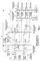
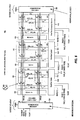
- FIG. 1 An exemplary hierarchical decoder incorporating at least two hierarchical multi-headed decoder circuits is shown in Fig. 1 , which shows a hierarchical multi-level multi-headed decoder circuit 100.
- a frst-level decoder circuit 102 generates a plurality of first-level decoded outputs 103, which are further decoded by a second-level decoding block 104. Each of these first-level decoded outputs 103 drives a respective second-level multi-headed decoder circuit 110.
- Each of these second-level multi-headed decoder circuits 110 includes a plurality of decoder "heads,” each of which drives a respective one of a plurality of second-level decoded outputs 105, which are further decoded by a third-level decoding block 106. Each of these second-level decoded outputs 105 drives a respective third-level multi-headed decoder circuit 130. Each of these third-level multi-headed decoder circuits 130 includes a plurality of decoder heads, each of which drives a respective one of a plurality of third-level decoded outputs 107.
- the third-level decoded outputs 107 may represent individual array lines of a memory array (e.g., word lines, bit lines), or may be indirectly coupled to such array lines of the memory array.
- each of the first-level decoded outputs is generated by decoding a portion of the row or column address appropriate for the decoder circuit 100.
- each of these first-level decoded outputs may also be level shifted, at least for certain modes of operation, by a respective level shifter 108, the motivation of which is described below in the context of several exemplary embodiments.
- the plurality of second-level multi-headed decoder circuits 110 are also responsive to a first plurality of bias circuits 120, 121 each respectively for generating one or more bias lines of a first type associated with a respective one of the decoder heads within the second-level multi-headed decoder circuit 110.
- a second plurality of bias circuits may also be utilized, each respectively for generating one or more bias lines of a second type associated with a respective one of the decoder heads within the second-level multi-headed decoder circuit 110.
- such second type of bias lines may be shared, and implemented as one or more bias lines shared by all decoder heads within the second-level multi-headed decoder circuit 110.
- Each of the bias circuits 120, 121 is responsive to at least a portion of the address information, and maybe further responsive to other control signals, such as mode of operation control signals.
- each of these bias circuits generates level shifted output levels on its respective bias lines, at least for certain modes of operation, and which outputs, as shown, may be complementary outputs.
- the bias lines driven by bias circuits 120, 121 are coupled to a corresponding decoder head in each second-level multi-headed decoder circuit 110.
- the plurality of third-level multi-headed decoder circuits 130 are also responsive to a first plurality of bias circuits (depicted within a first bias control circuit 134), each respectively for generating one or more bias lines of a first type associated with a respective one of the decoder heads within the third-level multi-headed decoder circuit 130.
- a second plurality of bias circuits may also be utilized (depicted within a second bias control circuit 136), each respectively for generating one or more bias lines of a second type associated with a respective one of the decoder heads within the second-level multi-headed decoder circuit 130.
- such second type of bias lines may be shared, and implemented as one or more bias lines shared by all decoder heads within the third-level multi-headed decoder circuit 130.
- each of these bias circuits is responsive to at least a portion of the address information, and may be further responsive to other control signals, such as mode of operation control signals.
- these bias circuits may generate level shifted output levels on one or more of its respective bias lines, at least for certain modes of operation.
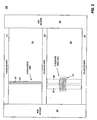
- Fig. 2 is a block diagram of an exemplary memory array 300.
- Two row decoders 302, 304 generate row select lines for the array, which each traverse across the array 300, as will be described herein.
- the word line driver circuits (not shown) are spatially distributed beneath the memory array and make connection to the word lines by way of vertical connections (one of which is labeled 310) on alternating sides of individual memory array blocks (two which are labeled 306, 308).
- the memory array is divided into two "stripes" 318, 320 by three column decoder and bit line circuit blocks 312, 314, 316, respectively at the top, middle, and bottom of the array.
- the bit lines within each stripe are also 2:1 interleaved to relax the pitch requirements of the column related circuitry.
- bit line 322 is associated with (i.e., driven and sensed by) the upper column circuit block 312, while bit line 324 is associated with the middle column circuits block 314.
- the memory array 300 is a three-dimensional memory array of passive element memory cells formed on each of four memory planes. Such memory cells preferably are antifuse cells. Each logical word line is connected to a word line segment on each of four word line layers (each associated with a respective memory plane).
- Other useful details of such an array 300 including exemplary memory cell technology and configurations, exemplary voltage conditions for reading and writing the array memory cells, exemplary power grid routing, exemplary distributed bias line discharge circuits, and exemplary bias circuit configurations for word line driver circuits, are further described in "Word Line Arrangement Having Multi-Layer Word Line Segments for Three-Dimensional Memory Array" by Roy E. Scheuerlein, U. S. Patent Application Publication No. 2004-0190360 A1 (now U. S. Patent No 6,879,505 ).
- Each stripe of the memory array 300 is divided into a large number of blocks, such as block 308.
- each block includes 288 bit lines on each of four bit line layers for the respective four memory planes, thus totaling 1,152 bit lines per block. These bit lines are 2:1 interleaved, so that each of the column decoders at the top and bottom of an array block interfaces to 576 bit lines.
- each block contains thirty-six 16-headed column decoders which select a total of 16 bit lines which are coupled respectively to 16 horizontal bus lines, which are then coupled respectively to 16 sense amplifiers.
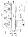
- XCSEL column select lines
- the thirty-six 16-headed column decoder circuits represent a plurality of third-level multi-headed decoder circuits, two of which are labeled 356 and 360.
- XCSEL signal 354 is selected (e.g., driven low)
- each of the sixteen decoder heads within the multi-headed decoder circuit 356 couples an associated bit line to a respective one of a group of sixteen bus lines i/O[0], iO[1], ... I/O[15].
- one such decoder head couples an associated bit line 362 to its associated bus line I/O[12] by way of a P-channel transistor 364.
- this head couples its associated bit line 362 to a common unselected bias line 368 associated with BLOCK 1 by way of an N-channel transistor 366.
- the sixteen selected bit lines are preferably arranged as four adjacent bit lines which exit the array at the top (or the bottom for the other decoder), on each of four bit line layers.
- the resultant pitch of each XCSEL line is therefore the pitch of eight bit lines within the memory block (because of the 2:1 interleaving).
- the XCSEL pitch is therefore 2.08 ⁇ m.
- the I/O[xx] bus lines may be grouped into four groups, as is depicted, which may be advantageous to facilitate independent bias conditions for bit lines on each bit line layer, particular during programming if not all of the sixteen "selected" bit lines are actually simultaneously programmed.
- the sixteen I/O lines traverse horizontally across all sixteen blocks. Each is coupled to a respective one of sixteen sense amplifier circuits which are distributed among the sixteen blocks as shown. For example, a first sense amplifier 370 is disposed within BLOCK 0 and is coupled to bus line I/O[0], a second sense amplifier 372 is disposed within BLOCK 1 and is coupled to bus line I/O[1], and a sixteenth sense amplifier 374 is disposed within BLOCK 15 and is coupled to bus line I/O[15].
- Each of the sixteen I/O lines may also be coupled to an associated bias circuit, which may be used during programming mode of operation to properly bias those bit lines to be programmed and those bit lines not to be programmed within the "selected" 16 bit lines. These bias circuits may be disabled and caused to exhibit a high output impedance during a read mode of operation when the selected bit lines are coupled to respective sense amplifiers.
- the memory array 300 may include one or more than one bays, and in some embodiments includes 4 bays within each array stripe. Contemplating the column decoder shown in addition to another identical column decoder for the bit lines exiting at the bottom of the array, in every group of 16 blocks (i.e., a bay) there are 32 sense amplifiers which connect to 32 selected bit lines. All the select bit lines are within one of the sixteen blocks, and no other bit lines are selected within the bay.
- the sense amplifiers may be conveniently implemented beneath the memory array block, whereas the bus lines I/O[xx], the sixteen-headed column select decoders (such as 360), and a small portion of the column decoders 352 are preferably implemented outside the array block.
- each of the column decoders 352 Each of the thirty-six second-level decoded outputs XCSEL is generated by a respective one of a group of thirty-six decoder heads, which may be viewed (within this block) as being arranged as nine 4-headed decoders coupled respectively to nine global column select lines CSG[0] through CSG[8]. These global column select lines CSG[xx] represent first level decoded outputs from a first level decoder 410, and are shared by all 16 blocks within the bay. In the figure, these thirty-six decoder heads are depicted as four groups of nine decoder heads, which represents a desired physical placement of such circuits, as described in the next figure below.
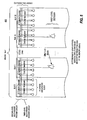
- bias circuit 416 includes a decoder portion 418 and a level shifter 417.
- the decoder portion 418 is responsive to appropriate column address signals CAD for selecting one of the four bias circuits within the block, and is also responsive to one or more block enable signals which may be common to all four bias circuits within the block.
- the level shifter 417 is used to variously shift the voltage levels of its output signals in accordance with certain operating modes, such as reading or programming.
- the first-level decoder 410 generates nine global column select lines, each being generated by a decoder portion 412 followed by a level shifter 411.
- Each decoder portion 412 is responsive to certain column address signals CAD, a control signal BAYE associated with the particular bay within which this block is disposed, and other control signals (e.g., PCHGCOL) to select one output thereof, which is level-shifted by the associated level shifter 411 to generate the selected global column select line, which is active high.
- a particular XCSEL driver is responsive to one of the nine global column address signals CSG[xx], is responsive to one of the four bias circuits, and also responsive to yet another bias line, in this case a power supply bus line conveying a column decoder voltage VCDEC.
- driver head 400 is responsive to CSG[0] and complementary bias nodes CQHV[3] and XCQHV[3] (and VCDEC), and generates XCSEL[27]. If CSG[0] is selected and therefore high, and CQHV[3] is selected and therefore low, then N-channel transistor 406 is conductive and drives XCSEL[27] low. P-channel transistor 404 remains off, as XCQHV[3] is high.
- P-channel transistors 402 and 404 is on, and pulls XCSEL[27] high to the VCDEC potential.
- transistor 404 pulls XCSEL[27] high to the VCDEC potential, irrespective of the state of CSG[0].
- transistor 402 pulls XCSEL[27] high to the VCDEC potential, irrespective of the state of CQHV[3] and XCQHV[3]. Consequently, only one XCSEL line is selected and driven to the low level generated by one of the bias circuits, and the remaining thirty-five XCSEL lines are driven to the VCDEC level.
- first-level decoder 410 and the bias circuits 414, 418 may be implemented beneath the memory array block (more exactingly, within the lateral extent of the memory array block), and only the XCSEL driver heads (e.g., 3-transistor driver head 400) are disposed outside the array block, thus improving the array efficiency.
- XCSEL driver heads e.g., 3-transistor driver head 400
- FIG. 5 an exemplary physical layout arrangement is depicted for the column decoder circuits described above for the 16 blocks within a bay. Given the description set forth above, such figure is believed to be self-explanatory, but a few salient points may be warranted.
- Four bias circuits are shown within each block. The complementary outputs each bias circuit traverse horizontally across, and serve decoder heads within, a respective one-fourth of the block. In contrast, the nine global column select lines CSG traverse across all 16 blocks, and serve decoder heads in all 16 blocks.
- the 16-headed column selectors (i.e., decoder heads 356 in Fig. 3 ) and the three-transistor XCSEL decoder heads 400 are shown implemented outside the array, while the bias circuits and the global column select line decoders are shown implemented beneath the array.
- each block (such as block 308) includes 4,096 addressable word lines, each including a word line segment on each of four word line layers, vertically connected together and to a word line driver disposed beneath the array blocks.
- additional word lines are included to support testing and redundancy, which adds, for example, 88 additional word lines per block, for a total of 4,184 word lines.
- These word lines are 2:1 interleaved, so that the word line decoding circuitry must interface to 2,092 word line connections (e.g., vertical connection 310) between each memory block.
- Every memory array block is associated with a respective plurality of 4-headed decoders on each side of the block.
- An individual 4-headed decoder on the left side of the block and a corresponding 4-headed decoder on the right side of the block are both responsive to a single decoded line from a common row select decoder, and together decode 1 out of 8 word lines within the block.
- FIG. 6 a block diagram is shown which represents an exemplary embodiment of a hierarchical, multi-level, multi-headed word line decoder circuit arrangement 500, which is intended to convey both certain circuit details and certain layout relationships of the various constituent blocks shown.
- Three memory blocks 502, 504,506 each include 4184 word lines.
- a four-headed word line driver 508 is shown to the left of block 504, and drives four word lines exiting memory block 504 to the left, while another four-headed word line driver 510 is shown to the right of block 504, and drives four word lines exiting memory block 504 to the right
- the word lines are 2:1 interleaved so that adjacent ones exit the block on opposite sides thereof
- Both four-headed word line drivers 508 and 510 are responsive to a single row select line RSEL[0] to decode and select 1 of 8 word lines in block 504.
- the four word lines associated with the four-headed word line driver 508 are common to two adjacent memory blocks 502, 504.
- a given four-headed word line driver decodes and drives four word lines in each of two adjacent blocks.
- these adjacent blocks may be viewed as being respectively to the left and to the right of the associated word line drivers.
- such four-headed word line drivers are disposed substantially beneath the array blacks, and only the vertical connections to the word lines made between the blocks.
- Each four-headed word line driver is responsive to an associated group of four "selected" bias lines and one unselected bias lines, all generated from an associated bias circuit.
- the four-headed word line driver 510 as well as the additional word line driver circuits associated with word lines in both blocks 504 and 506, all share a group of four selected bias lines XSEL ⁇ 0>, XSEL ⁇ 1>,... XSEL ⁇ 3>, and a common unselected bias line UXL generated by row bias circuit 514.
- the four-headed word line driver 508 as well as the additional word line driver circuits associated with word lines in both blocks 502 and 504, all share a respective group of four selected bias lines XSEL ⁇ 0>, XSEL ⁇ 1>, ...
- Each row bias circuit is also responsive to a two-bit portion of a row address RAD[2:1] to select which of the four heads is selected, responsive to a FLOAT signal for floating the selected and/or unselected bias lines during certain operation modes, and a VUX input conveying the voltage to which the UXL line, during certain modes of operation, is driven.
- a complementary group of four selected bias lines SEL ⁇ 0>, SEL ⁇ 1>, ... SEL ⁇ 3> are also shown, the selected one is which is driven high.
- Such lines may be used to accomplish a distributed grounding path through the selected memory block to better provide a robust local ground potential for the selected word line drivers.
- Such a distributed grounding circuit is described further in "Word Line Arrangement Having Multi-Layer Word Line Segments for Three-Dimensional Memory Array" by Roy E. Scheuerlein, U. S. Application No.10/403,844 filed March 31, 2003 , now published as U. S. Patent Application Publication No. 2004-0190360 A1 (now U. S. Patent No. 6,879,505 ).
- each word line driver includes a P-channel transistor (e.g., transistor 509) which couples its associated word line to the shared unselected bias line UXL associated therewith when the RSEL line is unselected (i.e., low), and further includes an N-channel transistor (e.g., transistor 511) which couples its associated word line to the associated one of the group of selected bias lines XSEL ⁇ 0>, XSEL ⁇ 1>, ... XSEL ⁇ 3> associated therewith when the RSEL line is selected (i.e., high).
- P-channel transistor e.g., transistor 509
- N-channel transistor e.g., transistor 511
- One of these selected bias lines is decoded and driven to a low level by the row bias circuit (assuming the associated memory block is selected), and the other three selected bias lines are driven with a voltage suitable for an unselected word line.
- a single selected RSEL line drives one word line low in the selected memory block, and drives the other seven word lines in the selected block to an unselected bias level, albeit by way of a "selected" bias node for the multi-headed drivers.
- all four selected bias nodes are driven to an unselected bias level so that no word lines are selected by the active RSEL line.
- the row select line RSEL[0] traverses across all the memory blocks in the entire memory stripe, and drives a respective four-headed word line driver located "between” each pair of blocks of the stripe (as well as two more, each respectively located “outside” the first and last blocks).
- a total of 512 such RSEL lines are likewise routed across the array and similarly coupled to respective plurality of four-headed word line drivers.
- Eleven additional RSEL lines are provided for the 88 test and redundant word lines, for a total of 523 RSEL lines (also known as "global row lines” and "global word lines”).
- these RSEL lines are driven at both ends thereof by two hierarchical row select decoders 520, 522 (also known as “global row decoders 520, 522”), each respectively located outside the array at left and right sides of the array stripe.
- two hierarchical row select decoders 520, 522 also known as “global row decoders 520, 522"
- the size of the global row decoder 520 is reduced, thus improving the array efficiency.
- a reverse decoding mode may be conveniently provided for improved testing capability, as further described in U. S. Application No. 11/026,493 filed December 30, 2004 entitled "Dual-Mode Decoder Circuit, Integrated Circuit Memory Array Incorporating Same, and Related Methods of Operation" by Kenneth K. So, Luca G. Fasoli, and Roy E. Scheuerlein.
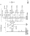
- FIG. 7 an exemplary embodiment of a portion of the global row decoders 520, 522 is depicted, which includes a four-headed decoder 552 for driving four global row lines, shown here labeled as RSEL[0], RSEL[1], RSEL[2], and RSEL[3].
- This four-headed decoder 552 may be viewed as a second-level multi-headed decoder circuit and is responsive to a first-level decoded output 556 (and its complementary output 557) from a first-level decoder 554.
- the first-level decoder 554 properly includes other portions not shown here, such as circuitry for generating a group of pre-decoded lines 573, described below.
- a NAND gate 572 receives a unique combination of four of the fourteen pre-decoded lines 573 to decode an active-low output which is then level-shifted by level shifter 571 to generate the complementary first-level decoded outputs 556, 557.
- the NAND gate 572 and level-shifter 571 are repeated (obviously with different unique combinations of the pre-decoded lines) to generate a respective first-level output for every four global row lines RSEL.
- the four-headed decoder 552, as well as the first-level decoder "slice” which includes a single NAND gate 572 and level-shifter 571 maybe viewed as together forming a row decoder cell RD_ROWDEC_4X, which is used repeatedly to implement the full global row line decoder, as described below.
- the four-headed decoder 552 is associated with four "selected" bias lines RDECB[3:0].
- the rationale for such a name is because a given decoder head couples its output to a "selected” bias line if the input to the decoder head is selected (i.e., driven to an active level). However, by no means does this imply that all four of the heads shown drive their respective outputs to a level that is reflective of the output being selected, because typically only one of the selected bias lines is actually biased in a condition suitable for a selected output, and the remaining three selected bias lines are biased in a condition suitable for an unselected output.
- the decoder heads shown include three transistors, including N-channel transistor 562 and P-channel transistor 563 which together form a circuit for coupling the decoder head output node to an associated one of a first group of bias lines, in this case the group of four bias lines RDECB[3:0].
- the one four-headed decoder 552 that is selected at any one time (i.e., whose input nodes 556 and 557 are respectively low and high) both of these transistors are on in each of the four decoder heads, and each head drives its output to whatever bias level is conveyed on the associated selected bias line to which the head is coupled, since the transistors 562, 563 form a full transfer gate.
- the decoder heads shown include an N-channel transistor 564 which may be viewed as forming a circuit for coupling the decoder head output node to an associated one of a second group of bias lines, in this case a group of only one shared bias line, which is a ground line.
- each of the four decoder heads drives its output to whatever bias level is conveyed on the associated unselected bias line to which the head is coupled, here a ground potential.
- FIG. 8 a higher-level view of global row decoder 520 is shown. This view also corresponds to the upper half of row decoder 302 shown in Fig. 2 . Multiple instantiations of the RD_ROWDEC_4X cell are implemented to generate all the necessary global row lines.
- a pre-decoder 582 (also labeled as a "Stage 1 Decoder") is shown which generates the pre-decoded lines 573 described above. Also shown in a Stage 2 Decoder and Comparator 584, which generates the four selected bias lines 558, 559, 560, 561 for the four-headed decoder 552 during normal read and programming operations.
- Such selected bias lines function as match lines in a reverse decoding mode for comparing the selected global row line driven by the other of the two global row decoders. Details of such operation, and other details of the Stage 2 Decoder and Comparator 584 are described in the aforementioned "Dual-Mode Decoder Circuit, Integrated Circuit Memory Array Incorporating Same, and Related Methods of Operation" by Kenneth K. So, Luca G. Fasoli, and Roy E. Scheuerlein.
- Exemplary bias conditions during programming for the cross-point array 300 are as follows: selected bit lines are driven to approximately 10 volts; unselected word lines are driven to approximately 9 volts; unselected bit lines are driven to approximately 1 volt, and selected word lines are driven to ground or near ground. This corresponds to a programming voltage of 10 volts. During a read mode of operation, the read voltage is approximately 2 volts. Additional description of suitable bias conditions and circuits for similar memory arrays may be found in "Multi-Headed Decoder Structure Utilizing Memory Array Line Driver with Dual Purpose Driver Device" by Roy E. Scheuerlein and Matthew P. Crowley, U. S. Patent Application Publication No. US 2003-0128581 A1 (now U. S. Patent No.
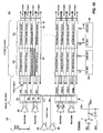
- FIG. 9 a block diagram depicts three memory array block 602, 604, 606.
- One word line decoder 608 includes a hierarchical decoder 610 whose decoded outputs drive a multi-headed inbound word line decoder 612 and a multi-headed outbound word line decoder 614.
- the hierarchical decoder 610 is conveniently implemented beneath the memory array block 604 (which is thus thought of as a row block), while the inbound word line decoder 612 and outbound word line decoder 614 are implemented outside the array block (i.e., between array blocks 604 and 606).
- another word line decoder includes a hierarchical decoder 620, a multi-headed inbound word line decoder 622, and a multi-headed outbound word line decoder 624.
- Word lines within the array block 604 are 2:1 interleaved, half being driven by the multi-headed inbound word line decoder 612, and the remaining half being driven by the multi-headed inbound word line decoder 622.
- the multi-headed outbound word line decoder 614 drives half of the word lines within array block 606 (the other half being driven by another outbound word line decoder not shown).
- No word line related circuitry is implemented beneath the array block 606, which area may instead be used for column support circuitry, and block 606 is thus thought of as a column block.
- This allows the row and column decoder circuits to be arranged in a checkerboard fashion, as is described in greater detail in U. S. Patent 6,567,287 to Roy E. Scheuerlein , entitled "Memory Device with Row and Column Decoder Circuits Arranged in a Checkerboard Pattern under a Plurality of Memory Arrays".
- the hierarchical decoder 610 generates a plurality of second-level decoded outputs XRS0, XRS 1, ... XRS(N), each of which drives a respective third-level 32-headed decoder circuit 654 for driving 32 word lines in an inbound direction, and further drives another respective third-level 32-headed decoder circuit 656 for driving 32 word lines in an outbound direction.
- the thirty-two word lines are preferably disposed as eight word lines on each of four word line layers of the memory array.
- the plurality of 32-headed decoder circuits 656 collectively forming the multi-headed outbound word line decoder 614 are associated with a bias generator circuit 658, which preferably generates thirty-two "selected” bias lines 660, and eight "unselected” bias lines 662. This allows the selected and unselected bias conditions for word lines on each word line layer to be easily controlled independently.
- a bias generator circuit 658 which preferably generates thirty-two "selected" bias lines 660, and eight "unselected” bias lines 662. This allows the selected and unselected bias conditions for word lines on each word line layer to be easily controlled independently.
- Another similar bias generator circuit 659 is also associated with the plurality of 32-headed decoder circuits 654 collectively forming the multi-headed inbound word line decoder 612.
- adjacent pairs of the 32-headed decoder circuits preferably are arranged so that the eight word lines (on each of four layers) associated with one such decoder (e.g., 656) overlay the eight word lines (on each of four layers) associated with the other such decoder (e.g., 657).
- Each of the second-level decoded output XRS[xx] lines is generated by a three-transistor decoder head 652 which is responsive to a complementary pair of level-shifted Block Enable signals received from a level-shifter 650, and further responsive to one of two "selected" bias lines XR0 and XR1.
- the "unselected" bias line for the decoder heads 652 is a shared bias line, in this case a decoder power supply line (which may convey different voltages depending upon the operating mode).
- the various Block Enable signals would be generated based upon decoding various row addresses, which may be viewed therefore as a first-level decoder circuit having a plurality of first-level decoded outputs (i.e., the complementary level-shifted block enable signals).
- Each of these decoded outputs then drives a second-level 2-headed decoder circuit, each head 652 of which drives a respective one of a plurality of second-level decoded outputs (i.e., XRS[xx]).
- each of these second-level decoded outputs then drives a third-level 64-headed decoder circuit (i.e., the 32-headed decoder circuit 654 and the 32-headed decoder circuit 656), each head of which drives a respective third level decoded output (i.e., an individual word line of the array).
- the decoder heads with the 32-headed decoder circuit 654, 656 are two-transistor word line drivers including a P-channel transistor coupling the respective word line to its associated selected bias line, and an N-channel transistor coupling the respective word line to its associated unselected bias line, both gated by the XRS[xx] signal.
- each NAND string includes a first select device coupling the NAND string to a global bit line, sixteen memory cell devices, and a second select device coupling the NAND string to a common source node or bias node.
- each NAND string requires 16 word lines and 2 select lines.
- all memory cells in each NAND string of a group of NAND strings sharing word lines are erased simultaneously. This group of memory cells defines an erase block.
- the Block Enable signals shown above correspond to an erase block (i.e., control 16 word lines (i.e., 8 word lines from this decoder, and 8 interleaved word line from the decoder on the opposite side of the memory block).
- the word lines belonging to the selected block are driven to either a selected voltage (e.g., V PROGRAM ) or an unselected voltage (e.g., V PASS ), which voltages are different from the selected voltage and an unselected voltage for all the other unselected strings (e.g., both of which may be preferably driven to ground).
- a selected XRS line preferably controls all eight word lines driven on one side of the block so that one memory cell transistor is driven to an appropriate selected condition (for reading or writing), while the other seven unselected memory cells are driven to an appropriate passing condition.
- a useful circuit and layout arrangement is shown for adjacent pairs of 32-headed decoders, such as decoder 656 and 657.
- decoder 656 twelve of the thirty-two decoder heads are shown, each responsive to the XRS2 signal. If the XRS2 signal is selected (ie., active low as shown here), then eight decoder heads are enabled to couple word lines WL0, WL1, ... WL7 on word line layer X0 to a respective selected bias signal generated by bias circuit 658. With eight heads all selected by the XRS2 decoded node, the bias circuit 658 can control all eight word lines on layer X0.
- decoder heads As shown, however, four of these eight decoder heads (driving word lines WL0-WL3) are disposed within the decoder 657, whereas the other four decoder heads (driving word lines WL4-WL7) are disposed within decoder 656. Similarly, if the XRS3 signal is selected, then eight decoder heads are enabled to couple word lines WL0, WL1, ... WL7 on word line layer X1 to the respective selected bias signals (labeled here as SELECT BIAS 0, 1, 2, ... 7) generated by bias circuit 658.
- decoder heads are disposed within the decoder 657, whereas the other four decoder heads (driving word lines WL4-WL7) are disposed within decoder 656.
- the pair of XRS lines alternate their connections to the decoder heads after each group of four decoder heads.
- a local unselected bias switch per erase block that selects between a ground level (for unselected strings) and a V PASS level (for the selected string), may also be employed to help provide suitable biasing conditions for all word lines in both selected and unselected memory blocks.
- a hierarchical multi-level, multi-headed decoder circuit may include more than two levels of multi-headed decoder circuits.
- bit lines usually every bit line includes the same number of memory cells.
- the number of bit lines, word lines, array blocks, and even memory planes is frequently an integral power of two in number (i.e., 2 N ), for ease and efficiency of decode circuitry.
- 2 N the number of bit lines, word lines, array blocks, and even memory planes
- word line segments on different layers may include different numbers of memory cells
- the memory array may include three memory planes
- word line segments within the first and last array block may be different in number of memory cells or bit line configuration, and any of many other irregular variations to the usual consistency of memory array design.
- top, left, bottom, and right are merely convenient descriptive terms for the four sides of a memory array.
- the word line segments for a block may be implemented as two interdigitated groups of word line segments oriented horizontally, and the bit lines for a block may be implemented as two interdigitated groups of bit lines oriented vertically.
- Each respective group of word lines or bit lines may be served by a respective decoder/driver circuit and a respective sense circuit on one of the four sides of the array.
- Suitable column circuits are set forth in "Tree Decoder Structure Particularly Well Suited to Interfacing Array Lines Having Extremely Small Layout Pitch," U. S. Patent Application No. 10/306,888, filed November 27, 2002 (now U. S. Patent No. 6,859,410 ).
- Word lines may also be referred to as row lines or X-lines, and bit lines may also be referred to as column lines or Y-lines.
- word lines may carry at least two different connotations to those skilled in the art.
- X-lines or word lines
- Y-lines or bit lines
- X-lines are usually contemplated as being connected to the gate terminal of memory cell transistors, or the switch terminal of the memory cell switch device, if present.
- the Y-lines (or bit lines) are usually contemplated as being connected to a switched terminal of the memory cell (e.g., source/drain terminal).
- the memory organization e.g., data bus width, number of bits simultaneously read during an operation, etc.
- the memory organization may have some association with viewing one set of the two array lines more aligned with data "bits" rather than data "words.” Consequently, the designations herein of X-lines, word lines, and row lines, and of Y-lines, bit lines, and column lines are illustrative of the various embodiments but should not be viewed in a restrictive sense, but rather a more general sense.
- word lines e.g., including word line segments
- bit lines usually represent orthogonal array lines, and generally follow a common assumption in the art that word lines are driven and bit lines are sensed, at least during a read operation.
- the bit lines of an array may also be referred to as sense lines of the array. No particular implication should be drawn as to word organization by use of such terms.
- a "global array line” e.g., a global word line, a global bit line
- a passive element memory array includes a plurality of 2-terminal memory cells, each connected between an associated X-line and an associated Y-line.
- Such a memory array may be a two-dimensional (planar) array or may be a three-dimensional array having more than one plane of memory cells.
- Each such memory cell has a non-linear conductivity in which the current in a reverse direction (i.e., from cathode to anode) is lower than the current in a forward direction.
- Application of a voltage from anode to cathode greater than a programming level changes the conductivity of the memory cell.
- the conductivity may decrease when the memory cell incorporates a fuse technology, or may increase when the memory cell incorporates an anti-fuse technology.
- a passive element memory array is not necessarily a one-time programmable (i.e., write once) memory array.
- Such passive element memory cells may generally be viewed as having a current steering element directing current in a direction and another component which is capable of changing its state (e.g., a fuse, an antifuse, a capacitor, a resistive element, etc.).
- the programming state of the memory element can be read by sensing current flow or voltage drop when the memory element is selected.
- Suitable three-dimensional anti-fuse memory cell structures, configurations, and processes include, without limitation, those described in: U. S. Patent 6,034,882 to Johnson, et al , entitled “Vertically Stacked Field Programmable Nonvolatile Memory and Method of Fabrication”; U. S. Patent 6,420,215 to Knall, et al , entitled “Three-Dimensional Memory Array and Method of Fabrication”; U. S. Patent 6,525,953 to Johnson , entitled “Vertically-Stacked, Field Programmable Nonvolatile Memory and Method of Fabrication”; U. S. Patent Application Publication No.
- the present invention is contemplated for advantageous use with any of a wide variety of memory cell technologies and memory array configurations, including both traditional single-level memory arrays and multi-level (i.e., three-dimensional) memory arrays, and particularly those having extremely dense X-line or Y-line pitch requirements.
- the memory cells may be comprised of semiconductor materials, as described in U. S. Patent 6,034,882 to Johnson et al. , and in U. S. Patent 5,835,396 to Zhang .
- an antifuse memory cell is contemplated.
- Other types of memory arrays, such as MRAM and organic passive element arrays, can also be used.
- MRAM magnetoresistive random access memory
- MRAM technology is described in " A 256kb 3.0V 1T1MTJ Nonvolatile Magnetoresistive RAM” by Peter K. Naji et al., published in the Digest of Technical Papers of the 2001 IEEE International Solid-State Circuits Conference, ISSCC 2001/Session 7/Technology Directions: Advanced Technologies/7.6, February 6,2001 and pages 94-95, 404-405 of ISSCC 2001 Visual Supplement.
- Certain passive element memory cells may be used which incorporate layers of organic materials including at least one layer that has a diode-like characteristic conduction and at least one organic material that changes conductivity with the application of an electric field.
- Patent 6,055,180 to Gudensen et aL describes such organic passive element arrays.
- Memory cells comprising materials such as phase-change materials and amorphous solids can also be used. See U. S. Patent 5,751,012 to Wolstenholme et al. , and U. S. Patent 4,646,266 to Ovshinsky et al .
- three-terminal memory cells may also be employed, rather than two-terminal passive element memory cells, and multiple X-lines (or row lines) selected to sum currents from more than one memory cell on a selected Y-line (or bit line).
- Such memory cells include flash EPROM and EEPROM cells, which are well known in the art Moreover, other memory array configurations having extremely dense X-line and/or Y-line pitch requirements are also contemplated such as, for example, those incorporating thin-film transistor (TFT) EEPROM memory cells, as described in "Dense Arrays and Charge Storage Devices, and Methods for Making Same," by Thomas H. Lee, et al., U. S. Patent Application Publication No. US 2002-0028541 A1 (now U. S. Patent No.
- TFT thin-film transistor
- an integrated circuit memory array is a monolithic integrated circuit structure, rather than more than one integrated circuit device packaged together or in close proximity.
- node may actually represent a pair of nodes for conveying a differential signal, or may represent multiple separate wires (e.g., a bus) for carrying several related signals or for carrying a plurality of signals forming a digital word or other multi-bit signal.
- circuits and physical structures are generally presumed, it is well recognized that in modern semiconductor design and fabrication, physical structures and circuits may be embodied in computer readable descriptive form suitable for use in subsequent design, test or fabrication stages as well as in resultant fabricated semiconductor integrated circuits. Accordingly, claims directed to traditional circuits or structures may, consistent with particular language thereof, read upon computer readable encodings and representations of same, whether embodied in media or combined with suitable reader facilities to allow fabrication, test, or design refinement of the corresponding circuits and/or structures.
- the invention is contemplated to include circuits, related methods or operation, related methods for making such circuits, and computer-readable medium encodings of such circuits and methods, all as described herein, and as defined in the appended claims.
- a computer-readable medium includes at least disk, tape, or other magnetic, optical, semiconductor (e.g., flash memory cards, ROM), or electronic medium and a network, wireline, wireless or other communications medium.
- An encoding of a circuit may include circuit schematic information, physical layout information, behavioral simulation information, and/or may include any other encoding from which the circuit may be represented or communicated.
Claims (21)
- Circuit intégré comportant :une matrice de mémoire (300) comportant des lignes de matrice (310, 322, 324, 362) d'un premier type et d'un second type couplées à des cellules de mémoire ; etun premier circuit décodeur hiérarchique (100) pour décoder des informations d'adresse et sélectionner une ou plusieurs lignes de matrice (310, 322, 324, 362) du premier type, ledit premier circuit décodeur hiérarchique (100) comportant au moins deux niveaux hiérarchiques (110, 130) de circuits décodeurs multitêtes ;dans lequel le premier circuit décodeur hiérarchique (100) comporte :un circuit décodeur de premier niveau (102) pour décoder une pluralité d'entrées de signaux d'adresse et générer une pluralité de sorties décodées de premier niveau (103) ; etune pluralité de circuits décodeurs multitêtes de deuxième niveau (110), chaque circuit respectif étant couplé à une sortie décodée de premier niveau (103) respective, chaque circuit décodeur multitête de deuxième niveau étant exploitable de manière à fournir une pluralité respective de sorties décodées de deuxième niveau (105) ;dans lequel chaque circuit respectif des circuits décodeurs multitêtes de deuxième niveau (110) comporte une pluralité respective de circuits pilotes de deuxième niveau (112, 113) et un premier noeud de polarisation respectif (558-561), chaque circuit pilote de deuxième niveau (112, 113) comportant :une entrée couplée à la sortie respective des sorties décodées de premier niveau (103) ; etune sortie couplée à la sortie correspondante de la pluralité respective de sorties décodées de deuxième niveau (105) ; etdans lequel le premier circuit décodeur hiérarchique (100) comporte en outre une première pluralité de circuits de polarisation de deuxième niveau (414, 416) pour générer respectivement un état pertinent sur les premiers noeuds de polarisation respectifs (558-561) des circuits décodeurs multitêtes de deuxième niveau (110), dans lequel l'état pertinent sur le premier noeud de polarisation (558-561) est, à certains moments, un état de polarisation de sortie décodée de deuxième niveau sélectionné ;caractérisé en ce que :chaque circuit respectif des circuits décodeurs multitêtes de deuxième niveau (110) comporte en outre un second noeud de polarisation (564) respectif ;le premier circuit décodeur hiérarchique (100) comporte en outre un second circuit de polarisation de deuxième niveau pour générer respectivement un état pertinent sur le second noeud de polarisation (564), dans lequel l'état pertinent sur le second noeud de polarisation (564) est un état de polarisation de sortie décodée de deuxième niveau non sélectionné ; etchaque circuit pilote de deuxième niveau (112, 113) est agencé de manière à connecter sa sortie au premier noeud de polarisation (558-561) si la sortie décodée de premier niveau couplée à son entrée est sélectionnée et, sinon, à connecter sa sortie au second noeud de polarisation (564).
- Circuit intégré selon la revendication 1, dans lequel la matrice de mémoire (300) comporte une matrice de mémoire tridimensionnelle présentant au moins deux plans de mémoire, ladite matrice de mémoire comportant :une pluralité respective de lignes de matrice du premier type sur chacune d'au moins une couche de lignes de matrice ; etune pluralité respective de lignes de matrice du second type sur chacune d'au moins une couche de lignes de matrice.
- Circuit intégré selon la revendication 1, dans lequel les circuits pilotes de deuxième niveau (112, 113) comportent respectivement :un premier circuit transistorisé destiné à coupler la sortie du circuit pilote de deuxième niveau aux premiers noeuds de polarisation respectifs lorsque la sortie décodée de premier niveau couplée à l'entrée est sélectionnée ; etun deuxième circuit transistorisé destiné à coupler la sortie du circuit pilote de deuxième niveau au second noeud de polarisation lorsque la sortie décodée de premier niveau couplée à l'entrée est non sélectionnée.
- Circuit intégré selon la revendication 3, dans lequel le premier circuit transistorisé comporte deux dispositifs transistorisés connectés en parallèle de type de conductivité opposée.
- Circuit intégré selon la revendication 3, dans lequel le deuxième circuit transistorisé comporte au moins deux dispositifs transistorisés connectés en parallèle commandés par des signaux distincts.
- Circuit intégré selon la revendication 1, comportant en outre une pluralité de circuits décodeurs multitêtes de troisième niveau (130), chaque circuit respectif étant couplé à une sortie décodée de deuxième niveau respective (105), chacune pour fournir une pluralité respective de sorties décodées de troisième niveau (107) couplées à la matrice de mémoire (300), chacun des circuits décodeurs multitêtes de troisième niveau (130) comportant un circuit pilote de troisième niveau, dans lequel chaque circuit pilote de troisième niveau comporte :une entrée couplée à la sortie respective des sorties décodées de deuxième niveau (105) ; etune sortie couplée à la sortie correspondante de la pluralité respective de sorties décodées de troisième niveau (107) ;chaque circuit pilote de troisième niveau (130) étant agencé de manière à coupler sa sortie à une ligne associée d'une pluralité de troisièmes lignes de bus, à certains moments, lorsque la sortie décodée de deuxième niveau couplée à son entrée est sélectionnée, et sinon, à coupler sa sortie à un noeud associé d'une pluralité de quatrièmes noeuds de polarisation.
- Circuit intégré selon la revendication 6, dans lequel le premier circuit décodeur hiérarchique (102) comporte en outre :une première pluralité de circuits de polarisation de troisième niveau pour générer respectivement, à certains moments, un état pertinent sur la pluralité de troisièmes lignes de bus ; etune seconde pluralité de circuits de polarisation de troisième niveau pour générer respectivement un état pertinent sur la pluralité de quatrièmes noeuds de polarisation ;dans lequel l'état pertinent sur au moins l'une des troisièmes lignes de bus est, à certains moments, un état de polarisation de sortie décodée de troisième niveau sélectionné ; etdans lequel l'état pertinent sur au moins une autre des troisièmes lignes de bus est, à certains moments, un état de polarisation de sortie décodée de troisième niveau non sélectionné.
- Circuit intégré selon la revendication 7, dans lequel l'état pertinent sur au moins l'une des troisièmes lignes de bus est, à certains moments, un état de noeud flottant.
- Circuit intégré selon la revendication 7, dans lequel :l'état pertinent sur au moins l'un des quatrièmes noeuds de polarisation est, à certains moments, un état de polarisation de sortie décodée de troisième niveau non sélectionné ; etl'état pertinent sur au moins un autre des quatrièmes noeuds de polarisation est, à certains moments, un état de noeud flottant.
- Circuit intégré selon la revendication 7, dans lequel les circuits pilotes de troisième niveau comportent respectivement :un troisième circuit transistorisé destiné à coupler la sortie du circuit pilote de troisième niveau à la ligne associée de la pluralité de troisièmes lignes de bus lorsque la sortie décodée de deuxième niveau couplée à l'entrée est sélectionnée ; etun quatrième circuit transistorisé destiné à coupler la sortie du circuit pilote de troisième niveau au noeud associé de la pluralité de quatrièmes noeuds de polarisation lorsque la sortie décodée de deuxième niveau couplée à l'entrée est non sélectionnée.
- Circuit intégré selon la revendication 10, dans lequel au moins l'un du troisième circuit transistorisé et du quatrième circuit transistorisé comporte au moins deux dispositifs transistorisés connectés en parallèle de type de conductivité opposée, et commandés par des signaux distincts.
- Circuit intégré selon la revendication 1, dans lequel les sorties décodées de deuxième niveau transitent à travers sensiblement l'ensemble de la matrice de mémoire (300).
- Circuit intégré selon la revendication 1, dans lequel les sorties décodées de deuxième niveau sont commandées à une tension supérieure à la tension VDD pour au moins l'un parmi un état de polarisation sélectionné et un état de polarisation non sélectionné.
- Circuit intégré selon la revendication 1, dans lequel :la matrice de mémoire (300) comporte une matrice tridimensionnelle présentant au moins deux plans de mémoire disposés au-dessus d'un substrat, et présentant en outre une pluralité respective de lignes de matrice (310, 322, 324, 362) du premier type sur au moins une couche de lignes de matrice, et présentant une pluralité respective de lignes de matrice (310, 322, 324, 362) du second type sur au moins une couche de lignes de matrice ; etau moins une pluralité des circuits décodeurs multitêtes de deuxième niveau est disposée sensiblement au sein de l'étendue latérale de la matrice de mémoire.
- Circuit intégré selon la revendication 6, dans lequel la pluralité de circuits décodeurs multitêtes de troisième niveau (130) est disposée sensiblement à l'extérieur de la matrice de mémoire (300).
- Circuit intégré selon la revendication 15, dans lequel :le circuit décodeur de premier niveau (102) est disposé au-dessous de la matrice de mémoire ; etles circuits pilotes de troisième niveau sont chacun respectivement constitués de deux dispositifs transistorisés.
- Circuit intégré selon la revendication 15, dans lequel :la pluralité de circuits décodeurs multitêtes de deuxième niveau (110) est disposée sensiblement à l'extérieur de la matrice de mémoire ;les sorties décodées de troisième niveau comportent des lignes de bits dans la matrice de mémoire (300), couplées chacune à une pluralité associée de cellules de mémoire dans la matrice de mémoire (300) ; etla pluralité de troisièmes lignes de bus est respectivement couplée à un bus de lecture/écriture respectif.
- Circuit intégré selon la revendication 6, dans lequel :la pluralité de circuits décodeurs multitêtes de deuxième niveau (110) est disposée sensiblement à l'extérieur de la matrice de mémoire (300) ; etla pluralité de circuits décodeurs multitêtes de troisième niveau (130) est disposée sensiblement au-dessous de la matrice de mémoire (300).
- Circuit intégré selon la revendication 18, dans lequel les sorties décodées de troisième niveau (107) comportent des lignes de mots (310) dans la matrice de mémoire (300), couplées chacune à une pluralité associée de cellules de mémoire, lesdites cellules de mémoire comportant des cellules de mémoire antifusibles à élément passif.
- Circuit intégré selon la revendication 1, dans lequel :la pluralité de circuits pilotes de deuxième niveau au sein d'un circuit décodeur multitête de deuxième niveau (110) est agencée en des groupes de tels circuits pilotes de deuxième niveau, les circuits pilotes de deuxième niveau individuels au sein d'un groupe étant respectivement couplés à un noeud respectif de la pluralité de premiers noeuds de polarisation, mais étant couplés ensemble à un noeud respectif de la pluralité de seconds noeuds de polarisation partagés par le groupe.
- Circuit intégré selon la revendication 6, dans lequel les circuits décodeurs multitêtes de troisième niveau (130) comportent chacun au moins 16 circuits pilotes de troisième niveau, lesdits au moins 16 circuits pilotes de troisième niveau de chaque circuit décodeur multitête de troisième niveau (130) étant configurés dans au moins quatre groupes d'au moins quatre circuits pilotes, chaque groupe partageant une ligne de polarisation non sélectionnée commune.
Priority Applications (1)
| Application Number | Priority Date | Filing Date | Title |
|---|---|---|---|
| EP11184470.0A EP2450902B1 (fr) | 2004-12-30 | 2005-12-16 | Appareil et procédé pour le décodage hiérarchique de réseaux de mémoire denses utilisant plusieurs niveaux de décodeurs à plusieurs têtes |
Applications Claiming Priority (2)
| Application Number | Priority Date | Filing Date | Title |
|---|---|---|---|
| US11/026,470 US7286439B2 (en) | 2004-12-30 | 2004-12-30 | Apparatus and method for hierarchical decoding of dense memory arrays using multiple levels of multiple-headed decoders |
| PCT/US2005/045564 WO2006073735A1 (fr) | 2004-12-30 | 2005-12-16 | Appareil et procede de decodage hierarchique de matrices memoires utilisant plusieurs niveaux de decodeurs a tetes multiples |
Related Child Applications (2)
| Application Number | Title | Priority Date | Filing Date |
|---|---|---|---|
| EP11184470.0A Division-Into EP2450902B1 (fr) | 2004-12-30 | 2005-12-16 | Appareil et procédé pour le décodage hiérarchique de réseaux de mémoire denses utilisant plusieurs niveaux de décodeurs à plusieurs têtes |
| EP11184470.0A Division EP2450902B1 (fr) | 2004-12-30 | 2005-12-16 | Appareil et procédé pour le décodage hiérarchique de réseaux de mémoire denses utilisant plusieurs niveaux de décodeurs à plusieurs têtes |
Publications (3)
| Publication Number | Publication Date |
|---|---|
| EP1831891A1 EP1831891A1 (fr) | 2007-09-12 |
| EP1831891A4 EP1831891A4 (fr) | 2008-11-12 |
| EP1831891B1 true EP1831891B1 (fr) | 2015-07-08 |
Family
ID=36640233
Family Applications (2)
| Application Number | Title | Priority Date | Filing Date |
|---|---|---|---|
| EP11184470.0A Active EP2450902B1 (fr) | 2004-12-30 | 2005-12-16 | Appareil et procédé pour le décodage hiérarchique de réseaux de mémoire denses utilisant plusieurs niveaux de décodeurs à plusieurs têtes |
| EP05854312.5A Active EP1831891B1 (fr) | 2004-12-30 | 2005-12-16 | Appareil et procede de decodage hierarchique de matrices memoires utilisant plusieurs niveaux de decodeurs a tetes multiples |
Family Applications Before (1)
| Application Number | Title | Priority Date | Filing Date |
|---|---|---|---|
| EP11184470.0A Active EP2450902B1 (fr) | 2004-12-30 | 2005-12-16 | Appareil et procédé pour le décodage hiérarchique de réseaux de mémoire denses utilisant plusieurs niveaux de décodeurs à plusieurs têtes |
Country Status (6)
| Country | Link |
|---|---|
| US (2) | US7286439B2 (fr) |
| EP (2) | EP2450902B1 (fr) |
| JP (1) | JP5032336B2 (fr) |
| KR (1) | KR101194353B1 (fr) |
| CN (2) | CN101138047B (fr) |
| WO (1) | WO2006073735A1 (fr) |
Families Citing this family (67)
| Publication number | Priority date | Publication date | Assignee | Title |
|---|---|---|---|---|
| US7286439B2 (en) * | 2004-12-30 | 2007-10-23 | Sandisk 3D Llc | Apparatus and method for hierarchical decoding of dense memory arrays using multiple levels of multiple-headed decoders |
| US7298665B2 (en) * | 2004-12-30 | 2007-11-20 | Sandisk 3D Llc | Dual-mode decoder circuit, integrated circuit memory array incorporating same, and related methods of operation |
| US7177191B2 (en) * | 2004-12-30 | 2007-02-13 | Sandisk 3D Llc | Integrated circuit including memory array incorporating multiple types of NAND string structures |
| US7272052B2 (en) * | 2005-03-31 | 2007-09-18 | Sandisk 3D Llc | Decoding circuit for non-binary groups of memory line drivers |
| US7345907B2 (en) * | 2005-07-11 | 2008-03-18 | Sandisk 3D Llc | Apparatus and method for reading an array of nonvolatile memory cells including switchable resistor memory elements |
| US7362604B2 (en) * | 2005-07-11 | 2008-04-22 | Sandisk 3D Llc | Apparatus and method for programming an array of nonvolatile memory cells including switchable resistor memory elements |
| KR100855861B1 (ko) * | 2005-12-30 | 2008-09-01 | 주식회사 하이닉스반도체 | 비휘발성 반도체 메모리 장치 |
| JP2007213732A (ja) * | 2006-02-13 | 2007-08-23 | Matsushita Electric Ind Co Ltd | 半導体記憶装置 |
| US7542337B2 (en) * | 2006-07-31 | 2009-06-02 | Sandisk 3D Llc | Apparatus for reading a multi-level passive element memory cell array |
| US7596050B2 (en) * | 2006-07-31 | 2009-09-29 | Sandisk 3D Llc | Method for using a hierarchical bit line bias bus for block selectable memory array |
| US7499366B2 (en) | 2006-07-31 | 2009-03-03 | Sandisk 3D Llc | Method for using dual data-dependent busses for coupling read/write circuits to a memory array |
| US7463536B2 (en) * | 2006-07-31 | 2008-12-09 | Sandisk 3D Llc | Memory array incorporating two data busses for memory array block selection |
| US7570523B2 (en) * | 2006-07-31 | 2009-08-04 | Sandisk 3D Llc | Method for using two data busses for memory array block selection |
| US7542338B2 (en) * | 2006-07-31 | 2009-06-02 | Sandisk 3D Llc | Method for reading a multi-level passive element memory cell array |
| US7554832B2 (en) * | 2006-07-31 | 2009-06-30 | Sandisk 3D Llc | Passive element memory array incorporating reversible polarity word line and bit line decoders |
| WO2008016932A2 (fr) * | 2006-07-31 | 2008-02-07 | Sandisk 3D Llc | Procédé et appareil pour un ensemble de mémoire d'élément passif incorporant des décodeurs de lignes de mots et de lignes binaires à polarité réversible |
| US8279704B2 (en) | 2006-07-31 | 2012-10-02 | Sandisk 3D Llc | Decoder circuitry providing forward and reverse modes of memory array operation and method for biasing same |
| WO2008016948A2 (fr) * | 2006-07-31 | 2008-02-07 | Sandisk 3D Llc | Procédé et appareil destinés à deux bus dépendant des données utiles pour coupler des circuits de lecture/écriture à un réseau de mémoires |
| US7486587B2 (en) * | 2006-07-31 | 2009-02-03 | Sandisk 3D Llc | Dual data-dependent busses for coupling read/write circuits to a memory array |
| US7633828B2 (en) * | 2006-07-31 | 2009-12-15 | Sandisk 3D Llc | Hierarchical bit line bias bus for block selectable memory array |
| US7463546B2 (en) * | 2006-07-31 | 2008-12-09 | Sandisk 3D Llc | Method for using a passive element memory array incorporating reversible polarity word line and bit line decoders |
| US7447071B2 (en) * | 2006-11-08 | 2008-11-04 | Atmel Corporation | Low voltage column decoder sharing a memory array p-well |
| US7542370B2 (en) * | 2006-12-31 | 2009-06-02 | Sandisk 3D Llc | Reversible polarity decoder circuit |
| US7525869B2 (en) * | 2006-12-31 | 2009-04-28 | Sandisk 3D Llc | Method for using a reversible polarity decoder circuit |
| US7468916B2 (en) * | 2007-03-20 | 2008-12-23 | Ememory Technology Inc. | Non-volatile memory having a row driving circuit with shared level shift circuits |
| US7719919B2 (en) * | 2007-03-20 | 2010-05-18 | Kabushiki Kaisha Toshiba | Semiconductor memory device in which word lines are driven from either side of memory cell array |
| US7554406B2 (en) | 2007-03-31 | 2009-06-30 | Sandisk 3D Llc | Spatially distributed amplifier circuit |
| US7558140B2 (en) * | 2007-03-31 | 2009-07-07 | Sandisk 3D Llc | Method for using a spatially distributed amplifier circuit |
| WO2008148091A1 (fr) * | 2007-05-25 | 2008-12-04 | Marvell World Trade Ltd. | Architecture de décodeur de lignes de bits du type arbre pour matrice de mémoire du type non-ou |
| KR100898667B1 (ko) * | 2007-08-06 | 2009-05-22 | 주식회사 하이닉스반도체 | 반도체 메모리 소자 |
| KR101526317B1 (ko) * | 2008-05-09 | 2015-06-11 | 삼성전자주식회사 | 계층적 디코딩 장치 |
| US8130528B2 (en) | 2008-08-25 | 2012-03-06 | Sandisk 3D Llc | Memory system with sectional data lines |
| US8027209B2 (en) | 2008-10-06 | 2011-09-27 | Sandisk 3D, Llc | Continuous programming of non-volatile memory |
| US8279650B2 (en) | 2009-04-20 | 2012-10-02 | Sandisk 3D Llc | Memory system with data line switching scheme |
| US8050109B2 (en) | 2009-08-10 | 2011-11-01 | Sandisk 3D Llc | Semiconductor memory with improved memory block switching |
| US8233309B2 (en) * | 2009-10-26 | 2012-07-31 | Sandisk 3D Llc | Non-volatile memory array architecture incorporating 1T-1R near 4F2 memory cell |
| US8223525B2 (en) | 2009-12-15 | 2012-07-17 | Sandisk 3D Llc | Page register outside array and sense amplifier interface |
| US8213243B2 (en) | 2009-12-15 | 2012-07-03 | Sandisk 3D Llc | Program cycle skip |
| US8284608B2 (en) * | 2010-10-05 | 2012-10-09 | Nxp B.V. | Combined EEPROM/flash non-volatile memory circuit |
| US9053766B2 (en) | 2011-03-03 | 2015-06-09 | Sandisk 3D, Llc | Three dimensional memory system with intelligent select circuit |
| US8553476B2 (en) | 2011-03-03 | 2013-10-08 | Sandisk 3D Llc | Three dimensional memory system with page of data across word lines |
| US8374051B2 (en) | 2011-03-03 | 2013-02-12 | Sandisk 3D Llc | Three dimensional memory system with column pipeline |
| US8730754B2 (en) * | 2011-04-12 | 2014-05-20 | Micron Technology, Inc. | Memory apparatus and system with shared wordline decoder |
| US8699293B2 (en) * | 2011-04-27 | 2014-04-15 | Sandisk 3D Llc | Non-volatile storage system with dual block programming |
| US8913443B2 (en) | 2011-09-19 | 2014-12-16 | Conversant Intellectual Property Management Inc. | Voltage regulation for 3D packages and method of manufacturing same |
| US8891305B2 (en) | 2012-08-21 | 2014-11-18 | Micron Technology, Inc. | Apparatuses and methods involving accessing distributed sub-blocks of memory cells |
| US8902670B2 (en) | 2012-08-31 | 2014-12-02 | Kabushiki Kaisha Toshiba | Semiconductor memory device |
| US9025391B2 (en) * | 2012-11-27 | 2015-05-05 | Infineon Technologies Ag | Circuit arrangement and method for operating a circuit arrangement |
| US9001584B2 (en) | 2013-02-28 | 2015-04-07 | Micron Technology, Inc. | Sub-block decoding in 3D memory |
| US8947972B2 (en) | 2013-03-15 | 2015-02-03 | Sandisk 3D Llc | Dynamic address grouping for parallel programming in non-volatile memory |
| US8947944B2 (en) | 2013-03-15 | 2015-02-03 | Sandisk 3D Llc | Program cycle skip evaluation before write operations in non-volatile memory |
| US9711225B2 (en) | 2013-10-16 | 2017-07-18 | Sandisk Technologies Llc | Regrouping and skipping cycles in non-volatile memory |
| US9564215B2 (en) | 2015-02-11 | 2017-02-07 | Sandisk Technologies Llc | Independent sense amplifier addressing and quota sharing in non-volatile memory |
| US9542979B1 (en) | 2015-08-25 | 2017-01-10 | Macronix International Co., Ltd. | Memory structure |
| ITUB20153728A1 (it) * | 2015-09-18 | 2017-03-18 | St Microelectronics Srl | Decodificatore di riga per un dispositivo di memoria non volatile, avente ridotta occupazione di area |
| US9721663B1 (en) * | 2016-02-18 | 2017-08-01 | Sandisk Technologies Llc | Word line decoder circuitry under a three-dimensional memory array |
| JP2018045750A (ja) * | 2016-09-16 | 2018-03-22 | 東芝メモリ株式会社 | 半導体記憶装置 |
| KR102398205B1 (ko) | 2017-06-12 | 2022-05-16 | 삼성전자주식회사 | 오티피 메모리 셀을 포함하는 메모리 장치 및 그것의 프로그램 방법 |
| CN108962309B (zh) * | 2018-06-29 | 2021-12-28 | 西安交通大学 | 一种高能量利用率低功耗的堆叠sram阵列结构 |
| US10755768B2 (en) * | 2018-07-16 | 2020-08-25 | Taiwan Semiconductor Manufacturing Company, Ltd. | Semiconductor device including distributed write driving arrangement and method of operating same |
| US10861551B2 (en) | 2018-12-28 | 2020-12-08 | Micron Technology, Inc. | Memory cells configured to generate weighted inputs for neural networks |
| WO2020196765A1 (fr) * | 2019-03-26 | 2020-10-01 | パナソニック インテレクチュアル プロパティ コーポレーション オブ アメリカ | Procédé de codage de données en trois dimensions, procédé de décodage de données en trois dimensions, dispositif de codage de données en trois dimensions et dispositif de décodage de données en trois dimensions |
| US10818731B1 (en) * | 2019-06-19 | 2020-10-27 | Avalanche Technology, Inc. | Three-dimensional nonvolatile memory |
| KR20210036535A (ko) * | 2019-09-26 | 2021-04-05 | 에스케이하이닉스 주식회사 | 반도체 장치 |
| US11139023B1 (en) * | 2020-03-19 | 2021-10-05 | Micron Technologhy, Inc. | Memory operation with double-sided asymmetric decoders |
| CN113270130A (zh) * | 2020-05-29 | 2021-08-17 | 台湾积体电路制造股份有限公司 | 存储器设备 |
| CN113411103B (zh) * | 2021-05-26 | 2022-04-22 | 盛销邦(广州)物联科技有限公司 | 一种基于rf电子标签的密集读写解码器 |
Family Cites Families (53)
| Publication number | Priority date | Publication date | Assignee | Title |
|---|---|---|---|---|
| US2649204A (en) | 1950-11-27 | 1953-08-18 | Jr James M Brier | Combination sediment cup and drain plug for internal-combustion engines |
| US2649304A (en) | 1951-02-10 | 1953-08-18 | Paddock Pool Equipment Co | Aluminum springboard |
| US3154636A (en) * | 1962-03-23 | 1964-10-27 | Xerox Corp | Three dimensional display device |
| US4646266A (en) * | 1984-09-28 | 1987-02-24 | Energy Conversion Devices, Inc. | Programmable semiconductor structures and methods for using the same |
| US5250859A (en) * | 1991-09-27 | 1993-10-05 | Kaplinsky Cecil H | Low power multifunction logic array |
| US5285118A (en) * | 1992-07-16 | 1994-02-08 | International Business Machines Corporation | Complementary current tree decoder |
| US5655113A (en) * | 1994-07-05 | 1997-08-05 | Monolithic System Technology, Inc. | Resynchronization circuit for a memory system and method of operating same |
| US5751012A (en) * | 1995-06-07 | 1998-05-12 | Micron Technology, Inc. | Polysilicon pillar diode for use in a non-volatile memory cell |
| US5835396A (en) * | 1996-10-17 | 1998-11-10 | Zhang; Guobiao | Three-dimensional read-only memory |
| JPH10241400A (ja) * | 1997-02-26 | 1998-09-11 | Toshiba Corp | 半導体記憶装置 |
| US6256224B1 (en) * | 2000-05-03 | 2001-07-03 | Hewlett-Packard Co | Write circuit for large MRAM arrays |
| NO972803D0 (no) * | 1997-06-17 | 1997-06-17 | Opticom As | Elektrisk adresserbar logisk innretning, fremgangsmåte til elektrisk adressering av samme og anvendelse av innretning og fremgangsmåte |
| US6191999B1 (en) * | 1997-06-20 | 2001-02-20 | Fujitsu Limited | Semiconductor memory device with reduced power consumption |
| JP3571497B2 (ja) * | 1997-06-20 | 2004-09-29 | 富士通株式会社 | 半導体記憶装置 |
| US6185121B1 (en) * | 1998-02-26 | 2001-02-06 | Lucent Technologies Inc. | Access structure for high density read only memory |
| US6034882A (en) * | 1998-11-16 | 2000-03-07 | Matrix Semiconductor, Inc. | Vertically stacked field programmable nonvolatile memory and method of fabrication |
| US6762951B2 (en) * | 2001-11-13 | 2004-07-13 | Hitachi, Ltd. | Semiconductor integrated circuit device |
| US6901006B1 (en) * | 1999-07-14 | 2005-05-31 | Hitachi, Ltd. | Semiconductor integrated circuit device including first, second and third gates |
| TW587252B (en) * | 2000-01-18 | 2004-05-11 | Hitachi Ltd | Semiconductor memory device and data processing device |
| US6420215B1 (en) * | 2000-04-28 | 2002-07-16 | Matrix Semiconductor, Inc. | Three-dimensional memory array and method of fabrication |
| US6856572B2 (en) * | 2000-04-28 | 2005-02-15 | Matrix Semiconductor, Inc. | Multi-headed decoder structure utilizing memory array line driver with dual purpose driver device |
| US6567287B2 (en) * | 2001-03-21 | 2003-05-20 | Matrix Semiconductor, Inc. | Memory device with row and column decoder circuits arranged in a checkerboard pattern under a plurality of memory arrays |
| US6888750B2 (en) * | 2000-04-28 | 2005-05-03 | Matrix Semiconductor, Inc. | Nonvolatile memory on SOI and compound semiconductor substrates and method of fabrication |
| US6631085B2 (en) * | 2000-04-28 | 2003-10-07 | Matrix Semiconductor, Inc. | Three-dimensional memory array incorporating serial chain diode stack |
| EP2988331B1 (fr) * | 2000-08-14 | 2019-01-09 | SanDisk Technologies LLC | Dispositif de mémoire à semiconducteur |
| US6591394B2 (en) * | 2000-12-22 | 2003-07-08 | Matrix Semiconductor, Inc. | Three-dimensional memory array and method for storing data bits and ECC bits therein |
| US6407953B1 (en) * | 2001-02-02 | 2002-06-18 | Matrix Semiconductor, Inc. | Memory array organization and related test method particularly well suited for integrated circuits having write-once memory arrays |
| US7177181B1 (en) * | 2001-03-21 | 2007-02-13 | Sandisk 3D Llc | Current sensing method and apparatus particularly useful for a memory array of cells having diode-like characteristics |
| US6545898B1 (en) * | 2001-03-21 | 2003-04-08 | Silicon Valley Bank | Method and apparatus for writing memory arrays using external source of high programming voltage |
| US6618295B2 (en) * | 2001-03-21 | 2003-09-09 | Matrix Semiconductor, Inc. | Method and apparatus for biasing selected and unselected array lines when writing a memory array |
| US6522594B1 (en) * | 2001-03-21 | 2003-02-18 | Matrix Semiconductor, Inc. | Memory array incorporating noise detection line |
| JP4808856B2 (ja) * | 2001-04-06 | 2011-11-02 | 富士通セミコンダクター株式会社 | 半導体記憶装置 |
| US6584034B1 (en) * | 2001-04-23 | 2003-06-24 | Aplus Flash Technology Inc. | Flash memory array structure suitable for multiple simultaneous operations |
| KR100387527B1 (ko) * | 2001-05-23 | 2003-06-27 | 삼성전자주식회사 | 레이아웃 사이즈가 감소된 로우 디코더를 갖는 불휘발성반도체 메모리장치 |
| US6480424B1 (en) * | 2001-07-12 | 2002-11-12 | Broadcom Corporation | Compact analog-multiplexed global sense amplifier for RAMS |
| US6525953B1 (en) | 2001-08-13 | 2003-02-25 | Matrix Semiconductor, Inc. | Vertically-stacked, field-programmable, nonvolatile memory and method of fabrication |
| US6768685B1 (en) * | 2001-11-16 | 2004-07-27 | Mtrix Semiconductor, Inc. | Integrated circuit memory array with fast test mode utilizing multiple word line selection and method therefor |
| US7081377B2 (en) | 2002-06-27 | 2006-07-25 | Sandisk 3D Llc | Three-dimensional memory |
| US6859410B2 (en) * | 2002-11-27 | 2005-02-22 | Matrix Semiconductor, Inc. | Tree decoder structure particularly well-suited to interfacing array lines having extremely small layout pitch |
| US6954394B2 (en) * | 2002-11-27 | 2005-10-11 | Matrix Semiconductor, Inc. | Integrated circuit and method for selecting a set of memory-cell-layer-dependent or temperature-dependent operating conditions |
| US7233522B2 (en) * | 2002-12-31 | 2007-06-19 | Sandisk 3D Llc | NAND memory array incorporating capacitance boosting of channel regions in unselected memory cells and method for operation of same |
| US7005350B2 (en) * | 2002-12-31 | 2006-02-28 | Matrix Semiconductor, Inc. | Method for fabricating programmable memory array structures incorporating series-connected transistor strings |
| US7505321B2 (en) * | 2002-12-31 | 2009-03-17 | Sandisk 3D Llc | Programmable memory array structure incorporating series-connected transistor strings and methods for fabrication and operation of same |
| US6879505B2 (en) * | 2003-03-31 | 2005-04-12 | Matrix Semiconductor, Inc. | Word line arrangement having multi-layer word line segments for three-dimensional memory array |
| US7177183B2 (en) * | 2003-09-30 | 2007-02-13 | Sandisk 3D Llc | Multiple twin cell non-volatile memory array and logic block structure and method therefor |
| US20050128807A1 (en) * | 2003-12-05 | 2005-06-16 | En-Hsing Chen | Nand memory array incorporating multiple series selection devices and method for operation of same |
| US7023739B2 (en) * | 2003-12-05 | 2006-04-04 | Matrix Semiconductor, Inc. | NAND memory array incorporating multiple write pulse programming of individual memory cells and method for operation of same |
| US7221588B2 (en) * | 2003-12-05 | 2007-05-22 | Sandisk 3D Llc | Memory array incorporating memory cells arranged in NAND strings |
| KR100536613B1 (ko) * | 2004-04-09 | 2005-12-14 | 삼성전자주식회사 | 프로그램 시간을 단축할 수 있는 노어형 플래시 메모리장치 및 그것의 프로그램 방법 |
| US7203123B2 (en) * | 2004-12-08 | 2007-04-10 | Infineon Technologies Ag | Integrated DRAM memory device |
| US7298665B2 (en) * | 2004-12-30 | 2007-11-20 | Sandisk 3D Llc | Dual-mode decoder circuit, integrated circuit memory array incorporating same, and related methods of operation |
| US7286439B2 (en) * | 2004-12-30 | 2007-10-23 | Sandisk 3D Llc | Apparatus and method for hierarchical decoding of dense memory arrays using multiple levels of multiple-headed decoders |
| US7307268B2 (en) * | 2005-01-19 | 2007-12-11 | Sandisk Corporation | Structure and method for biasing phase change memory array for reliable writing |
-
2004
- 2004-12-30 US US11/026,470 patent/US7286439B2/en not_active Expired - Fee Related
-
2005
- 2005-12-16 KR KR1020077016213A patent/KR101194353B1/ko active IP Right Grant
- 2005-12-16 JP JP2007549434A patent/JP5032336B2/ja not_active Expired - Fee Related
- 2005-12-16 EP EP11184470.0A patent/EP2450902B1/fr active Active
- 2005-12-16 CN CN2005800451715A patent/CN101138047B/zh active Active
- 2005-12-16 CN CN2011100734317A patent/CN102201254B/zh active Active
- 2005-12-16 WO PCT/US2005/045564 patent/WO2006073735A1/fr active Application Filing
- 2005-12-16 EP EP05854312.5A patent/EP1831891B1/fr active Active
-
2007
- 2007-10-22 US US11/876,563 patent/US7633829B2/en active Active
Also Published As
| Publication number | Publication date |
|---|---|
| WO2006073735A1 (fr) | 2006-07-13 |
| US7286439B2 (en) | 2007-10-23 |
| CN102201254A (zh) | 2011-09-28 |
| CN101138047B (zh) | 2011-05-18 |
| JP5032336B2 (ja) | 2012-09-26 |
| EP2450902A3 (fr) | 2012-09-05 |
| EP1831891A4 (fr) | 2008-11-12 |
| CN102201254B (zh) | 2012-11-14 |
| KR20070110835A (ko) | 2007-11-20 |
| US7633829B2 (en) | 2009-12-15 |
| US20060146639A1 (en) | 2006-07-06 |
| JP2008527585A (ja) | 2008-07-24 |
| US20080101149A1 (en) | 2008-05-01 |
| CN101138047A (zh) | 2008-03-05 |
| KR101194353B1 (ko) | 2012-10-25 |
| EP2450902B1 (fr) | 2014-03-19 |
| EP2450902A2 (fr) | 2012-05-09 |
| EP1831891A1 (fr) | 2007-09-12 |
Similar Documents
| Publication | Publication Date | Title |
|---|---|---|
| EP1831891B1 (fr) | Appareil et procede de decodage hierarchique de matrices memoires utilisant plusieurs niveaux de decodeurs a tetes multiples | |
| US6856572B2 (en) | Multi-headed decoder structure utilizing memory array line driver with dual purpose driver device | |
| US6879505B2 (en) | Word line arrangement having multi-layer word line segments for three-dimensional memory array | |
| US6859410B2 (en) | Tree decoder structure particularly well-suited to interfacing array lines having extremely small layout pitch | |
| US8637870B2 (en) | Three-dimensional memory device incorporating segmented array line memory array | |
| US7272052B2 (en) | Decoding circuit for non-binary groups of memory line drivers | |
| US7554832B2 (en) | Passive element memory array incorporating reversible polarity word line and bit line decoders | |
| US8279704B2 (en) | Decoder circuitry providing forward and reverse modes of memory array operation and method for biasing same | |
| KR20090057231A (ko) | 가역 극성 워드 라인과 비트 라인 디코더를 결합한 패시브 엘리먼트 메모리 어레이용 방법과 장치 | |
| KR20090057374A (ko) | 메모리 어레이 블록 선택을 위하여 두 개의 데이터 버스를 통합한 메모리 어레이용 방법과 장치 |
Legal Events
| Date | Code | Title | Description |
|---|---|---|---|
| PUAI | Public reference made under article 153(3) epc to a published international application that has entered the european phase |
Free format text: ORIGINAL CODE: 0009012 |
|
| 17P | Request for examination filed |
Effective date: 20070615 |
|
| AK | Designated contracting states |
Kind code of ref document: A1 Designated state(s): AT BE BG CH CY CZ DE DK EE ES FI FR GB GR HU IE IS IT LI LT LU LV MC NL PL PT RO SE SI SK TR |
|
| DAX | Request for extension of the european patent (deleted) | ||
| A4 | Supplementary search report drawn up and despatched |
Effective date: 20081014 |
|
| 17Q | First examination report despatched |
Effective date: 20090928 |
|
| REG | Reference to a national code |
Ref country code: DE Ref legal event code: R079 Ref document number: 602005046938 Country of ref document: DE Free format text: PREVIOUS MAIN CLASS: G11C0005060000 Ipc: G11C0008100000 |
|
| GRAP | Despatch of communication of intention to grant a patent |
Free format text: ORIGINAL CODE: EPIDOSNIGR1 |
|
| RIC1 | Information provided on ipc code assigned before grant |
Ipc: G11C 16/08 20060101ALI20140903BHEP Ipc: G11C 8/10 20060101AFI20140903BHEP |
|
| INTG | Intention to grant announced |
Effective date: 20141001 |
|
| GRAP | Despatch of communication of intention to grant a patent |
Free format text: ORIGINAL CODE: EPIDOSNIGR1 |
|
| INTG | Intention to grant announced |
Effective date: 20150227 |
|
| GRAS | Grant fee paid |
Free format text: ORIGINAL CODE: EPIDOSNIGR3 |
|
| GRAA | (expected) grant |
Free format text: ORIGINAL CODE: 0009210 |
|
| AK | Designated contracting states |
Kind code of ref document: B1 Designated state(s): AT BE BG CH CY CZ DE DK EE ES FI FR GB GR HU IE IS IT LI LT LU LV MC NL PL PT RO SE SI SK TR |
|
| REG | Reference to a national code |
Ref country code: GB Ref legal event code: FG4D |
|
| REG | Reference to a national code |
Ref country code: AT Ref legal event code: REF Ref document number: 735931 Country of ref document: AT Kind code of ref document: T Effective date: 20150715 Ref country code: CH Ref legal event code: EP |
|
| REG | Reference to a national code |
Ref country code: IE Ref legal event code: FG4D |
|
| REG | Reference to a national code |
Ref country code: DE Ref legal event code: R096 Ref document number: 602005046938 Country of ref document: DE |
|
| REG | Reference to a national code |
Ref country code: AT Ref legal event code: MK05 Ref document number: 735931 Country of ref document: AT Kind code of ref document: T Effective date: 20150708 |
|
| REG | Reference to a national code |
Ref country code: NL Ref legal event code: MP Effective date: 20150708 |
|
| REG | Reference to a national code |
Ref country code: LT Ref legal event code: MG4D |
|
| PG25 | Lapsed in a contracting state [announced via postgrant information from national office to epo] |
Ref country code: LV Free format text: LAPSE BECAUSE OF FAILURE TO SUBMIT A TRANSLATION OF THE DESCRIPTION OR TO PAY THE FEE WITHIN THE PRESCRIBED TIME-LIMIT Effective date: 20150708 Ref country code: FI Free format text: LAPSE BECAUSE OF FAILURE TO SUBMIT A TRANSLATION OF THE DESCRIPTION OR TO PAY THE FEE WITHIN THE PRESCRIBED TIME-LIMIT Effective date: 20150708 Ref country code: GR Free format text: LAPSE BECAUSE OF FAILURE TO SUBMIT A TRANSLATION OF THE DESCRIPTION OR TO PAY THE FEE WITHIN THE PRESCRIBED TIME-LIMIT Effective date: 20151009 Ref country code: LT Free format text: LAPSE BECAUSE OF FAILURE TO SUBMIT A TRANSLATION OF THE DESCRIPTION OR TO PAY THE FEE WITHIN THE PRESCRIBED TIME-LIMIT Effective date: 20150708 |
|
| PG25 | Lapsed in a contracting state [announced via postgrant information from national office to epo] |
Ref country code: SE Free format text: LAPSE BECAUSE OF FAILURE TO SUBMIT A TRANSLATION OF THE DESCRIPTION OR TO PAY THE FEE WITHIN THE PRESCRIBED TIME-LIMIT Effective date: 20150708 Ref country code: PT Free format text: LAPSE BECAUSE OF FAILURE TO SUBMIT A TRANSLATION OF THE DESCRIPTION OR TO PAY THE FEE WITHIN THE PRESCRIBED TIME-LIMIT Effective date: 20151109 Ref country code: ES Free format text: LAPSE BECAUSE OF FAILURE TO SUBMIT A TRANSLATION OF THE DESCRIPTION OR TO PAY THE FEE WITHIN THE PRESCRIBED TIME-LIMIT Effective date: 20150708 Ref country code: AT Free format text: LAPSE BECAUSE OF FAILURE TO SUBMIT A TRANSLATION OF THE DESCRIPTION OR TO PAY THE FEE WITHIN THE PRESCRIBED TIME-LIMIT Effective date: 20150708 Ref country code: IS Free format text: LAPSE BECAUSE OF FAILURE TO SUBMIT A TRANSLATION OF THE DESCRIPTION OR TO PAY THE FEE WITHIN THE PRESCRIBED TIME-LIMIT Effective date: 20151108 Ref country code: PL Free format text: LAPSE BECAUSE OF FAILURE TO SUBMIT A TRANSLATION OF THE DESCRIPTION OR TO PAY THE FEE WITHIN THE PRESCRIBED TIME-LIMIT Effective date: 20150708 |
|
| REG | Reference to a national code |
Ref country code: DE Ref legal event code: R097 Ref document number: 602005046938 Country of ref document: DE |
|
| PG25 | Lapsed in a contracting state [announced via postgrant information from national office to epo] |
Ref country code: CZ Free format text: LAPSE BECAUSE OF FAILURE TO SUBMIT A TRANSLATION OF THE DESCRIPTION OR TO PAY THE FEE WITHIN THE PRESCRIBED TIME-LIMIT Effective date: 20150708 Ref country code: SK Free format text: LAPSE BECAUSE OF FAILURE TO SUBMIT A TRANSLATION OF THE DESCRIPTION OR TO PAY THE FEE WITHIN THE PRESCRIBED TIME-LIMIT Effective date: 20150708 Ref country code: IT Free format text: LAPSE BECAUSE OF FAILURE TO SUBMIT A TRANSLATION OF THE DESCRIPTION OR TO PAY THE FEE WITHIN THE PRESCRIBED TIME-LIMIT Effective date: 20150708 Ref country code: EE Free format text: LAPSE BECAUSE OF FAILURE TO SUBMIT A TRANSLATION OF THE DESCRIPTION OR TO PAY THE FEE WITHIN THE PRESCRIBED TIME-LIMIT Effective date: 20150708 Ref country code: DK Free format text: LAPSE BECAUSE OF FAILURE TO SUBMIT A TRANSLATION OF THE DESCRIPTION OR TO PAY THE FEE WITHIN THE PRESCRIBED TIME-LIMIT Effective date: 20150708 |
|
| PLBE | No opposition filed within time limit |
Free format text: ORIGINAL CODE: 0009261 |
|
| STAA | Information on the status of an ep patent application or granted ep patent |
Free format text: STATUS: NO OPPOSITION FILED WITHIN TIME LIMIT |
|
| PG25 | Lapsed in a contracting state [announced via postgrant information from national office to epo] |
Ref country code: RO Free format text: LAPSE BECAUSE OF FAILURE TO SUBMIT A TRANSLATION OF THE DESCRIPTION OR TO PAY THE FEE WITHIN THE PRESCRIBED TIME-LIMIT Effective date: 20150708 Ref country code: BE Free format text: LAPSE BECAUSE OF NON-PAYMENT OF DUE FEES Effective date: 20151231 |
|
| 26N | No opposition filed |
Effective date: 20160411 |
|
| PG25 | Lapsed in a contracting state [announced via postgrant information from national office to epo] |
Ref country code: LU Free format text: LAPSE BECAUSE OF FAILURE TO SUBMIT A TRANSLATION OF THE DESCRIPTION OR TO PAY THE FEE WITHIN THE PRESCRIBED TIME-LIMIT Effective date: 20151216 Ref country code: MC Free format text: LAPSE BECAUSE OF FAILURE TO SUBMIT A TRANSLATION OF THE DESCRIPTION OR TO PAY THE FEE WITHIN THE PRESCRIBED TIME-LIMIT Effective date: 20150708 |
|
| REG | Reference to a national code |
Ref country code: CH Ref legal event code: PL |
|
| REG | Reference to a national code |
Ref country code: DE Ref legal event code: R081 Ref document number: 602005046938 Country of ref document: DE Owner name: SANDISK TECHNOLOGIES LLC, PLANO, US Free format text: FORMER OWNER: SANDISK 3D LLC, MILPITAS, CALIF., US |
|
| GBPC | Gb: european patent ceased through non-payment of renewal fee |
Effective date: 20151216 |
|
| PG25 | Lapsed in a contracting state [announced via postgrant information from national office to epo] |
Ref country code: SI Free format text: LAPSE BECAUSE OF FAILURE TO SUBMIT A TRANSLATION OF THE DESCRIPTION OR TO PAY THE FEE WITHIN THE PRESCRIBED TIME-LIMIT Effective date: 20150708 |
|
| REG | Reference to a national code |
Ref country code: IE Ref legal event code: MM4A |
|
| REG | Reference to a national code |
Ref country code: FR Ref legal event code: ST Effective date: 20160831 |
|
| PG25 | Lapsed in a contracting state [announced via postgrant information from national office to epo] |
Ref country code: GB Free format text: LAPSE BECAUSE OF NON-PAYMENT OF DUE FEES Effective date: 20151216 Ref country code: LI Free format text: LAPSE BECAUSE OF NON-PAYMENT OF DUE FEES Effective date: 20151231 Ref country code: IE Free format text: LAPSE BECAUSE OF NON-PAYMENT OF DUE FEES Effective date: 20151216 Ref country code: CH Free format text: LAPSE BECAUSE OF NON-PAYMENT OF DUE FEES Effective date: 20151231 |
|
| PG25 | Lapsed in a contracting state [announced via postgrant information from national office to epo] |
Ref country code: FR Free format text: LAPSE BECAUSE OF NON-PAYMENT OF DUE FEES Effective date: 20151231 |
|
| PG25 | Lapsed in a contracting state [announced via postgrant information from national office to epo] |
Ref country code: BE Free format text: LAPSE BECAUSE OF FAILURE TO SUBMIT A TRANSLATION OF THE DESCRIPTION OR TO PAY THE FEE WITHIN THE PRESCRIBED TIME-LIMIT Effective date: 20150708 |
|
| PG25 | Lapsed in a contracting state [announced via postgrant information from national office to epo] |
Ref country code: BG Free format text: LAPSE BECAUSE OF FAILURE TO SUBMIT A TRANSLATION OF THE DESCRIPTION OR TO PAY THE FEE WITHIN THE PRESCRIBED TIME-LIMIT Effective date: 20150708 Ref country code: HU Free format text: LAPSE BECAUSE OF FAILURE TO SUBMIT A TRANSLATION OF THE DESCRIPTION OR TO PAY THE FEE WITHIN THE PRESCRIBED TIME-LIMIT; INVALID AB INITIO Effective date: 20051216 |
|
| PG25 | Lapsed in a contracting state [announced via postgrant information from national office to epo] |
Ref country code: NL Free format text: LAPSE BECAUSE OF FAILURE TO SUBMIT A TRANSLATION OF THE DESCRIPTION OR TO PAY THE FEE WITHIN THE PRESCRIBED TIME-LIMIT Effective date: 20150708 Ref country code: CY Free format text: LAPSE BECAUSE OF FAILURE TO SUBMIT A TRANSLATION OF THE DESCRIPTION OR TO PAY THE FEE WITHIN THE PRESCRIBED TIME-LIMIT Effective date: 20150708 |
|
| PG25 | Lapsed in a contracting state [announced via postgrant information from national office to epo] |
Ref country code: TR Free format text: LAPSE BECAUSE OF FAILURE TO SUBMIT A TRANSLATION OF THE DESCRIPTION OR TO PAY THE FEE WITHIN THE PRESCRIBED TIME-LIMIT Effective date: 20150708 |
|
| PGFP | Annual fee paid to national office [announced via postgrant information from national office to epo] |
Ref country code: DE Payment date: 20221018 Year of fee payment: 18 |
|
| P01 | Opt-out of the competence of the unified patent court (upc) registered |
Effective date: 20230606 |