EP1811557A2 - Semiconductor apparatus manufacturing method - Google Patents
Semiconductor apparatus manufacturing method Download PDFInfo
- Publication number
- EP1811557A2 EP1811557A2 EP07000718A EP07000718A EP1811557A2 EP 1811557 A2 EP1811557 A2 EP 1811557A2 EP 07000718 A EP07000718 A EP 07000718A EP 07000718 A EP07000718 A EP 07000718A EP 1811557 A2 EP1811557 A2 EP 1811557A2
- Authority
- EP
- European Patent Office
- Prior art keywords
- connecting portion
- semiconductor apparatus
- manufacturing
- electrode
- laser
- Prior art date
- Legal status (The legal status is an assumption and is not a legal conclusion. Google has not performed a legal analysis and makes no representation as to the accuracy of the status listed.)
- Withdrawn
Links
Images





Classifications
-
- H—ELECTRICITY
- H10—SEMICONDUCTOR DEVICES; ELECTRIC SOLID-STATE DEVICES NOT OTHERWISE PROVIDED FOR
- H10W—GENERIC PACKAGES, INTERCONNECTIONS, CONNECTORS OR OTHER CONSTRUCTIONAL DETAILS OF DEVICES COVERED BY CLASS H10
- H10W70/00—Package substrates; Interposers; Redistribution layers [RDL]
- H10W70/40—Leadframes
- H10W70/481—Leadframes for devices being provided for in groups H10D8/00 - H10D48/00
-
- H—ELECTRICITY
- H10—SEMICONDUCTOR DEVICES; ELECTRIC SOLID-STATE DEVICES NOT OTHERWISE PROVIDED FOR
- H10W—GENERIC PACKAGES, INTERCONNECTIONS, CONNECTORS OR OTHER CONSTRUCTIONAL DETAILS OF DEVICES COVERED BY CLASS H10
- H10W72/00—Interconnections or connectors in packages
- H10W72/071—Connecting or disconnecting
- H10W72/076—Connecting or disconnecting of strap connectors
-
- H—ELECTRICITY
- H10—SEMICONDUCTOR DEVICES; ELECTRIC SOLID-STATE DEVICES NOT OTHERWISE PROVIDED FOR
- H10W—GENERIC PACKAGES, INTERCONNECTIONS, CONNECTORS OR OTHER CONSTRUCTIONAL DETAILS OF DEVICES COVERED BY CLASS H10
- H10W99/00—Subject matter not provided for in other groups of this subclass
-
- H—ELECTRICITY
- H10—SEMICONDUCTOR DEVICES; ELECTRIC SOLID-STATE DEVICES NOT OTHERWISE PROVIDED FOR
- H10W—GENERIC PACKAGES, INTERCONNECTIONS, CONNECTORS OR OTHER CONSTRUCTIONAL DETAILS OF DEVICES COVERED BY CLASS H10
- H10W72/00—Interconnections or connectors in packages
- H10W72/071—Connecting or disconnecting
- H10W72/073—Connecting or disconnecting of die-attach connectors
- H10W72/07331—Connecting techniques
- H10W72/07336—Soldering or alloying
-
- H—ELECTRICITY
- H10—SEMICONDUCTOR DEVICES; ELECTRIC SOLID-STATE DEVICES NOT OTHERWISE PROVIDED FOR
- H10W—GENERIC PACKAGES, INTERCONNECTIONS, CONNECTORS OR OTHER CONSTRUCTIONAL DETAILS OF DEVICES COVERED BY CLASS H10
- H10W72/00—Interconnections or connectors in packages
- H10W72/071—Connecting or disconnecting
- H10W72/073—Connecting or disconnecting of die-attach connectors
- H10W72/07331—Connecting techniques
- H10W72/07337—Connecting techniques using a polymer adhesive, e.g. an adhesive based on silicone or epoxy
-
- H—ELECTRICITY
- H10—SEMICONDUCTOR DEVICES; ELECTRIC SOLID-STATE DEVICES NOT OTHERWISE PROVIDED FOR
- H10W—GENERIC PACKAGES, INTERCONNECTIONS, CONNECTORS OR OTHER CONSTRUCTIONAL DETAILS OF DEVICES COVERED BY CLASS H10
- H10W72/00—Interconnections or connectors in packages
- H10W72/071—Connecting or disconnecting
- H10W72/076—Connecting or disconnecting of strap connectors
- H10W72/07631—Techniques
- H10W72/07632—Compression bonding, e.g. thermocompression bonding
- H10W72/07633—Ultrasonic bonding, e.g. thermosonic bonding
-
- H—ELECTRICITY
- H10—SEMICONDUCTOR DEVICES; ELECTRIC SOLID-STATE DEVICES NOT OTHERWISE PROVIDED FOR
- H10W—GENERIC PACKAGES, INTERCONNECTIONS, CONNECTORS OR OTHER CONSTRUCTIONAL DETAILS OF DEVICES COVERED BY CLASS H10
- H10W72/00—Interconnections or connectors in packages
- H10W72/071—Connecting or disconnecting
- H10W72/076—Connecting or disconnecting of strap connectors
- H10W72/07631—Techniques
- H10W72/07635—Applying EM radiation, e.g. induction heating or using a laser
-
- H—ELECTRICITY
- H10—SEMICONDUCTOR DEVICES; ELECTRIC SOLID-STATE DEVICES NOT OTHERWISE PROVIDED FOR
- H10W—GENERIC PACKAGES, INTERCONNECTIONS, CONNECTORS OR OTHER CONSTRUCTIONAL DETAILS OF DEVICES COVERED BY CLASS H10
- H10W72/00—Interconnections or connectors in packages
- H10W72/071—Connecting or disconnecting
- H10W72/076—Connecting or disconnecting of strap connectors
- H10W72/07651—Connecting or disconnecting of strap connectors characterised by changes in properties of the strap connectors during connecting
- H10W72/07652—Connecting or disconnecting of strap connectors characterised by changes in properties of the strap connectors during connecting changes in structures or sizes
-
- H—ELECTRICITY
- H10—SEMICONDUCTOR DEVICES; ELECTRIC SOLID-STATE DEVICES NOT OTHERWISE PROVIDED FOR
- H10W—GENERIC PACKAGES, INTERCONNECTIONS, CONNECTORS OR OTHER CONSTRUCTIONAL DETAILS OF DEVICES COVERED BY CLASS H10
- H10W72/00—Interconnections or connectors in packages
- H10W72/071—Connecting or disconnecting
- H10W72/076—Connecting or disconnecting of strap connectors
- H10W72/07651—Connecting or disconnecting of strap connectors characterised by changes in properties of the strap connectors during connecting
- H10W72/07653—Connecting or disconnecting of strap connectors characterised by changes in properties of the strap connectors during connecting changes in shapes
-
- H—ELECTRICITY
- H10—SEMICONDUCTOR DEVICES; ELECTRIC SOLID-STATE DEVICES NOT OTHERWISE PROVIDED FOR
- H10W—GENERIC PACKAGES, INTERCONNECTIONS, CONNECTORS OR OTHER CONSTRUCTIONAL DETAILS OF DEVICES COVERED BY CLASS H10
- H10W72/00—Interconnections or connectors in packages
- H10W72/50—Bond wires
- H10W72/531—Shapes of wire connectors
- H10W72/533—Cross-sectional shape
- H10W72/534—Cross-sectional shape being rectangular
-
- H—ELECTRICITY
- H10—SEMICONDUCTOR DEVICES; ELECTRIC SOLID-STATE DEVICES NOT OTHERWISE PROVIDED FOR
- H10W—GENERIC PACKAGES, INTERCONNECTIONS, CONNECTORS OR OTHER CONSTRUCTIONAL DETAILS OF DEVICES COVERED BY CLASS H10
- H10W72/00—Interconnections or connectors in packages
- H10W72/60—Strap connectors, e.g. thick copper clips for grounding of power devices
- H10W72/621—Structures or relative sizes of strap connectors
- H10W72/627—Multiple strap connectors having different structures or shapes
-
- H—ELECTRICITY
- H10—SEMICONDUCTOR DEVICES; ELECTRIC SOLID-STATE DEVICES NOT OTHERWISE PROVIDED FOR
- H10W—GENERIC PACKAGES, INTERCONNECTIONS, CONNECTORS OR OTHER CONSTRUCTIONAL DETAILS OF DEVICES COVERED BY CLASS H10
- H10W72/00—Interconnections or connectors in packages
- H10W72/60—Strap connectors, e.g. thick copper clips for grounding of power devices
- H10W72/631—Shapes of strap connectors
-
- H—ELECTRICITY
- H10—SEMICONDUCTOR DEVICES; ELECTRIC SOLID-STATE DEVICES NOT OTHERWISE PROVIDED FOR
- H10W—GENERIC PACKAGES, INTERCONNECTIONS, CONNECTORS OR OTHER CONSTRUCTIONAL DETAILS OF DEVICES COVERED BY CLASS H10
- H10W72/00—Interconnections or connectors in packages
- H10W72/60—Strap connectors, e.g. thick copper clips for grounding of power devices
- H10W72/651—Materials of strap connectors
- H10W72/652—Materials of strap connectors comprising metals or metalloids, e.g. silver
-
- H—ELECTRICITY
- H10—SEMICONDUCTOR DEVICES; ELECTRIC SOLID-STATE DEVICES NOT OTHERWISE PROVIDED FOR
- H10W—GENERIC PACKAGES, INTERCONNECTIONS, CONNECTORS OR OTHER CONSTRUCTIONAL DETAILS OF DEVICES COVERED BY CLASS H10
- H10W72/00—Interconnections or connectors in packages
- H10W72/851—Dispositions of multiple connectors or interconnections
- H10W72/853—On the same surface
- H10W72/871—Bond wires and strap connectors
-
- H—ELECTRICITY
- H10—SEMICONDUCTOR DEVICES; ELECTRIC SOLID-STATE DEVICES NOT OTHERWISE PROVIDED FOR
- H10W—GENERIC PACKAGES, INTERCONNECTIONS, CONNECTORS OR OTHER CONSTRUCTIONAL DETAILS OF DEVICES COVERED BY CLASS H10
- H10W72/00—Interconnections or connectors in packages
- H10W72/90—Bond pads, in general
- H10W72/921—Structures or relative sizes of bond pads
- H10W72/926—Multiple bond pads having different sizes
-
- H—ELECTRICITY
- H10—SEMICONDUCTOR DEVICES; ELECTRIC SOLID-STATE DEVICES NOT OTHERWISE PROVIDED FOR
- H10W—GENERIC PACKAGES, INTERCONNECTIONS, CONNECTORS OR OTHER CONSTRUCTIONAL DETAILS OF DEVICES COVERED BY CLASS H10
- H10W74/00—Encapsulations, e.g. protective coatings
-
- H—ELECTRICITY
- H10—SEMICONDUCTOR DEVICES; ELECTRIC SOLID-STATE DEVICES NOT OTHERWISE PROVIDED FOR
- H10W—GENERIC PACKAGES, INTERCONNECTIONS, CONNECTORS OR OTHER CONSTRUCTIONAL DETAILS OF DEVICES COVERED BY CLASS H10
- H10W90/00—Package configurations
- H10W90/701—Package configurations characterised by the relative positions of pads or connectors relative to package parts
- H10W90/751—Package configurations characterised by the relative positions of pads or connectors relative to package parts of bond wires
- H10W90/756—Package configurations characterised by the relative positions of pads or connectors relative to package parts of bond wires between a chip and a stacked lead frame, conducting package substrate or heat sink
-
- H—ELECTRICITY
- H10—SEMICONDUCTOR DEVICES; ELECTRIC SOLID-STATE DEVICES NOT OTHERWISE PROVIDED FOR
- H10W—GENERIC PACKAGES, INTERCONNECTIONS, CONNECTORS OR OTHER CONSTRUCTIONAL DETAILS OF DEVICES COVERED BY CLASS H10
- H10W90/00—Package configurations
- H10W90/701—Package configurations characterised by the relative positions of pads or connectors relative to package parts
- H10W90/761—Package configurations characterised by the relative positions of pads or connectors relative to package parts of strap connectors
- H10W90/766—Package configurations characterised by the relative positions of pads or connectors relative to package parts of strap connectors between a chip and a stacked lead frame, conducting package substrate or heat sink
Definitions
- the present invention relates to a manufacturing method of a semiconductor apparatus including a semiconductor chip and an electrode which is formed on the semiconductor chip and electrically connected with an external lead and, particularly, to a manufacturing method of a semiconductor apparatus capable of carrying a large current.
- MOSFETs Metal-Oxide-Semiconductor Field-Effect Transistors
- MOSFETs which are used for power supply in consumer-electronics products such as cell phones, personal computers, and digital audiovisual equipments or for driving a motor of vehicles, carry a high current of about 5 to 200 A. It thus requires a thick, heavy wire material. For example, a plurality of large-gauge wires of about 100 to 500 ⁇ m are connected to the source electrode of a MOSFET in order to draw a high current.
- connection of a bonding wire to the source electrode by ultrasonic bonding or thermocompression bonding requires a bonding area of about 1.5 to 3 times the wire cross-sectional area.
- the area of the source electrode or the gate electrode is limited to small and thus subject to the limitation by the wire cross-sectional area.
- high pressure application is required to obtain a large bonding strength, and the mechanical impact causes a decrease in yields. This is described in Japanese Unexamined Patent Application Publication No. 2002-313851 (Oono ), for example.
- a plate-shaped electrical path member is bonded by ultrasonic to thereby obtain a large bonding strength and achieve high yields.
- Fig 8 is a bird's-eye view of a semiconductor apparatus (Small Out-line Package (SOP) - 8 packages) taught by Oono.
- Figs. 9A and 9B are cross sectional views along lines IVA-IVA and IVB-IVB, respectively, in Fig. 8.
- the MOSFET 101 is almost entirely fixed and covered by a sealing resin (molding resin) 102 which is made of epoxy resin or the like.
- the MOSFET 101 has eight leads 103, such that one end of each lead 103 is exposed outside the molding resin 102.
- the molding resin 102 includes a semiconductor device (semiconductor chip) 105.
- a source electrode (source pad) 104s and a gate electrode (gate pad) 104g are formed on the top surface, and a drain electrode (drain pad), though not shown, is formed at the end of the under surface.
- the four terminals arranged on one side out of the terminals of the eight leads 103 are integrated into one set inside the molding resin 102.
- the four terminals serve as drain-side terminals 103d of the leads 103 which are to be electrically connected with the drain pad.
- the remaining four terminals out of the terminals of the eight leads 103 are arranged so as to avoid direct contact with the semiconductor device 105 and to be electrically disconnected from the drain-side terminals 103d and the lead 103 including a drain-side post 107d inside the molding resin 102 as shown in Fig. 9A.
- Out of the remaining four terminals of the leads 103 three terminals are integrated into one set, and the remaining one terminal is electrically disconnected from those three-in-one terminals of the lead 103.
- the thee-in-one terminals of the lead 103 are electrically connected with the source electrode 104s of the semiconductor device 105 by a current path member 106 to serve as source-side terminals 103s of the leads 103.
- the remaining one terminal of the lead 103 is electrically connected with the gate electrode 104g of the semiconductor device 105 by a single bonding wire 108 to serve as a gate-side terminal 103g of the lead 103.
- an electrode-side connecting portion 106a which is formed at one end is connected by plane with the source electrode 104s, and a lead-side connecting portion 106b which is formed at the other end is connected by plane with a source-side post 107s.
- the current path member 106 is directly connected to both the source electrode 104s and the source-side post 107s of each source-side terminal 103s of the leads 103 at the same time by ultrasonic bonding.
- the semiconductor apparatus 101 taught by Oono allows the cross sectional area of the current path flowing between the source electrode 104s of the semiconductor device 105 and the source-side post 107s of each source-side terminal 103s of the leads 103 to be significantly larger than a total of the cross sectional area of the current path flowing through a plurality of bonding wires in a conventional MOSFET. This enables the MOSFET 101 to have significantly lower resistance between the source electrode 104c and the lead 103 compared with a conventional MOSFET.
- the bonding process may be carried out at the temperature of about 300°C, for example, so that an oxide film is formed on metal. Further, the temperature in the bonding process is low compared with the melting point of a metal such as a wire member, which is 800°C to 1100°C. Thus, a mechanical energy is required in order to break the oxide film formed on a wire member and to enable bonding with the low temperature in the bonding process between the electrode and the wire material. In such a case, mechanical vibration is applied so as to break the oxide film and expose a new surface, which cause damage to the chip. Particularly, a MOSFET has an active cell below the pad, and the damage caused by the ultrasonic vibration can reach the element below the pad, which leads to breakdown of a product. Further, because the process forms an alloy by mechanical contact, the bonding is not appropriate for some types of metal.
- the technique of laser bonding can cause damage to a base below the electrode.
- large-gauge wires of about 100 to 500 ⁇ m or above are used to reduce the resistance in order for the MOSFET to carry a high current. This corresponds to the thickness of 100 to 500 ⁇ m.
- the thickness of the electrode to be connected is as small as about 2 to 6 ⁇ m as described in Oono.
- the adjustment of laser intensity is extremely difficult when laser-welding the members having different thicknesses, and it is impossible to provide bonding by the laser welding. High laser intensity to fuse the wire causes breakdown of the base, and low laser intensity fails to establish connection or obtain desired connection intensity.
- a manufacturing method of a semiconductor apparatus including a semiconductor chip and an electrode formed on the semiconductor chip and electrically connected with an external lead. This method laser-welds the electrode with a thin-film shaped connecting area formed partly or entirely on a connecting portion electrically connected with the external lead.
- the method makes the laser welding between the semiconductor chip and the external lead through the connecting portion. It uses a thin-film shaped connecting area which is formed partly or entirely on the connecting portion, thereby enabling laser welding with an electrode which is normally significantly thinner than the connecting portion. This achieves the establishment of electrical connection without mechanical vibration.
- the present invention provides a semiconductor apparatus manufacturing method which enables an increase in productivity and yields and exhibits high electrical operability and reliability.
- the present invention is applied to a semiconductor apparatus for carrying a high current which is used for power supply or switches in cell phones, motors and so on, in which a number of MOSFETs are combined into one MOSFET. While a single transistor normally carries a current of about 0.1A, such a transistor can carry a current of about 5 to 200A and can be used for power supply in consumer-electronics products, motor driving in vehicles or the like.
- Fig. 1A is a perspective view of a semiconductor apparatus according to an embodiment of the present invention.
- Figs. 1B and 1C are cross-sectional views along line IB-IB in Fig. 1A.
- a semiconductor apparatus 1 includes a die pad (island) 2 formed on a lead frame, a semiconductor chip (die) 3 which is mounted on the die pad 2, and a lead frame 4 which is electrically connected with the semiconductor chip 3.
- these elements are covered with a molding resin made of epoxy resin or the like and packaged entirely except for one end (outer lead (external lead) 4b) of the lead frame 4.
- the lead frame 4 includes a portion for mounting the semiconductor chip 3 (which is referred to as the die pad or the internal lead) and a portion projecting outside of the package and soldered to a substrate (which is referred to as the external lead) . Because a different feature is required for each portion, the die pad and the internal lead may be nickel-plated or non-plated, and the external lead may be solder- or tin- plated, for example.
- the semiconductor chip 3 may be formed of a vertical MOSFET, for example.
- a drain electrode though not shown, is formed on its under surface and connected to the die pad 2.
- An external lead also not shown, which is connected with the die pad 2 serves as a drain-side terminal.
- On the upper surface of the semiconductor chip 3 are formed a source electrode (electrode pad) 3a and a gate electrode (electrode pad) 3b.
- a connecting portion 4a having a thin-film shape (flat-plate or ribbon-like shape) which is formed at the end of the internal lead of the lead frame 4 is electrically connected with the source electrode 3a and the gate electrode 3b.
- the lead frame 4 is not plated.
- the lead frame 4 includes a base 41 such as Cu and a plating layer 42 such as Ni which is formed on the base 41.
- the connecting portion 4a of the lead frame 4 is bonded by laser welding with the source electrode 3a and the gate electrode 3b, and one or a plurality of weld-bonding portions 5 are provided depending on the bonding area.
- the use of laser welding for connection facilitates the positioning between the lead frame 4 and the semiconductor chip 3 and thus enables easier manufacturing such as one-time connection using a galvanometer mirror or the like.
- the connecting member such as the internal lead or the wire and the electrodes on the semiconductor chip 3 cannot be laser-welded simply. While the thickness of the electrode on the semiconductor chip 3 is typically about 4 to 5 ⁇ m, the thickness of the connecting member such the wire is about several tens to hundreds times greater. If a thickness ratio of the members to be welded differs largely, the use of high laser power with the intent to weld those members can result in breakdown of the base underneath. On the other hand, the use of low laser power fails to establish connection or obtain desired connection intensity. Thus, the breakdown of the elements below the electrode can occur unless optimizing the thickness of the connecting portion with respect to the thickness of the electrode.
- the technique of using the ribbon-like or flat-plate connecting member and performing the ultrasonic bonding as disclosed in Oono causes the element to be subject to breakdown due to the mechanical vibration, and the ultrasonic bonding of a large area requires a large-scale machine to increase manufacturing costs.
- a connecting member and electrodes on the semiconductor chip 3 can be laser-welded by forming at least a part of the connecting member to be electrically connected with the electrode, which is referred to hereinafter as the connecting portion, into a thin-film shape (flat-plate or ribbon-like shape) and minimizing a difference (ratio) in thickness between the connecting portion and the electrodes.
- the lead frame 4 of this embodiment has the connecting portion 4a having a thin-film shape which is thinner than the other part.
- the laser welding is applied between the connecting portion 4a and the electrodes 3a and 3b.
- the connecting portion 4a is not necessarily entirely thin-film shaped.
- the laser welding is possible with equal effect as long as at least an area to be laser-welded, which is a part of the connecting portion 4a, is thin-film shaped to serve as a welding area.
- connection intensity can be obtained by laser welding without damaging the base below the electrodes by setting the thickness of the connecting portion 4a to be less than thirty times the thickness of the electrodes 3a and 3b on the semiconductor chip 3.
- the thickness of the connecting portion 4a is preferably 5 to 30 times, more preferably 10 to 20 times, the thickness of the electrodes 3a and 3b.
- the connecting portion 4a when using laser welding, it is preferred to set an appropriate thickness ratio between the connecting portion 4a and the electrodes 3a and 3b. If the thickness of the connecting portion 4a is more than thirty times the thickness of the electrodes 3a and 3b, high laser power is required for the laser welding. This can cause damage underneath the electrode, which leads to breakdown of the element. Specifically, the laser fusing of the thick connecting portion 4a can cause the laser to penetrate through the thin electrodes 3a and 3b to break down the base underneath.
- the laser can undesirably reach beyond the depth of 5 ⁇ m, or, even if the laser does not reach beyond the electrode thickness range, undesirable variation occurs in the bonding strength or the like. It is thus preferred that the thickness of the connecting member is less than 30 times the thickness of the electrode.
- the thickness of the connecting portion 4a is preferably equal to or more than 5 times the thickness of the electrodes 3a and 3b, or more preferably equal to or more than 10 times to obtain more stable intensity.
- the thickness of the connecting portion 4a of the lead frame 4 is preferably about 25 to 150 ⁇ m.
- the contact area of the connecting portion 4a with the electrodes 3a and 3b based on the thickness of the connecting portion 4a and the current flowing through the electrodes 3a and 3b. It is further preferred to determine the contact area based on a prescribed electrical resistance in the connecting portion between the connecting portion 4a and the electrodes 3a and 3b.
- the semiconductor apparatus may carry a current of 5 to 200 A, and it is preferred to design the sizes of the connecting portion 4a and the electrodes 3a and 3b such that the contact area is in accordance with desired current and resistance values.
- the contact area indicates the area where the connecting portion 4a is actually in contact with the electrodes 3a and 3b, not the area of the entire connecting portion 4a.
- the connecting portion 4a is laser-welded at a plurality of points, and the part surrounded by the outermost weld-bonding portions 5 serves as the contact area.
- the electrical resistance of the contacting portion 4a is preferably low for smaller current loss.
- the semiconductor apparatus (MOSFET) 1 controls ON/OFF of a switch by a prescribed resistance value, the resistance to enable the switching function is required at least. It is thus preferred to determine the thickness of the connecting portion 4a and the contact area based on the resistance value necessary to serve as a switch.
- the area of the connecting portion 4a may be larger than the area of the electrodes 3a and 3b.
- Fig. 2 is a cross sectional view along line II-II in Fig. 1A. As shown in Fig. 2, the electrode 3a is formed on the semiconductor chip 3 which is mounted on the die pad 2.
- a nonconductive cover layer 6 which may be made of polymide (PI), phosphate glass (PSG), an oxide film or the like is formed in the vicinity of the electrode 3a to cover the elements around the electrode 3a. This prevents the connecting portion 4a from being electrically continuous with other elements even if the connecting portion 4a is larger than the actual area of the electrode 3a. This further facilitates the positioning between the connecting portion 4a and the electrodes 3a and 3b because of the connecting portion 4a being large.
- the connecting portion 4a (lead frame 4) is typically formed of aluminum, copper, or an alloy of those.
- the use of gold, silver, palladium, or an alloy of those is also possible. Further, a metal material may be formed on the surface of such a connecting member.
- the copper is particularly suitable for use as a connecting member because of its high conductivity; however, it has low laser absorbency. Therefore, for easier laser welding, it is possible to provide the plating of nickel (Ni) having high laser absorbency on the surface of copper or form an alloy of Ni and copper.
- a gate electrode is formed below a source electrode (lead electrode) with an insulating film interposed therebetween.
- the insulating film may be formed of oxide silicon glass (BPSG: borophosphorous silicate glass) added with phosphorous and boron, PSG (phosphorous silicate glass) or the like. If damage is applied to the insulating film by laser welding, the MOSFET becomes inoperable. It is therefore preferred that the insulating film as the base is formed of a heat resistant material.
- a beam to bridge the lead frame 4 and the electrodes 3a and 3b is formed by bending or the like.
- the shape of the end of the lead frame 4 (connecting portion 4a) may be adjusted appropriately according to the chip size.
- the connecting part decreases to enable the provision of more reliable semiconductor apparatus.
- the connecting portion 4a and the electrodes 3a and 3b are connected by ultrasonic bonding, it is necessary to make oscillation at a bonding portion. This requires the positioning between the connecting portion 4a and the electrodes 3a and 3b with an accuracy of about ⁇ 25 ⁇ m.
- the laser welding which is employed in this embodiment, assures good bonding with the positioning accuracy of about ⁇ 100 ⁇ m. Because of such a rough positioning accuracy required, the number of times to check the lead or chip position for the positioning can be reduced to thereby lower the manufacturing costs.
- the laser welding fuses the metal of the connecting portion 4a of the lead frame 4 and the electrodes 3a and 3b completely for connection, thus enabling the bonding of dissimilar metals.
- UBM underbump metal
- the bonding by the laser welding does not apply any mechanical stress, thus not causing damage to the semiconductor chip 3 to thereby increase yields.
- the laser welding is a normal temperature process in which heat is generated only in the welding portion, it does not cause oxidation of the lead frame 4 or the semiconductor chip 3.
- This embodiment uses an external lead (lead frame) 4 whose end is shaped into the thin-film connecting portion 4a.
- the lead frame 4 of such a shape can be obtained by forming the thin-film shaped connecting portion 4a simultaneously during molding. This enables the formation of the lead frame 4 with the thin-film shaped connecting portion 4a to enable laser welding without any additional step.
- the connecting portion 4a is formed at the end of the lead frame 4 so as to have a given thickness and the size and shape according to the electrodes 3a and 3b of the semiconductor chip 3.
- the semiconductor chip 3 is mounted on the die pad 2.
- the die pad 2 and the semiconductor chip 3 may be electrically connected by soldering, silver paste, or the like.
- the lead frame 4 is placed thereon so that the connecting portion 4a of the lead frame 4 and the electrodes 3a and 3b on the semiconductor chip 3 are placed on one another.
- the positioning accuracy may be about ⁇ 100 ⁇ m because they are to be bonded by laser welding.
- a laser is applied to partly fuse the connecting portion 4a of the lead frame 4 and the electrodes 3a and 3b to thereby weld the metals.
- the connecting portion 4a and the source electrode 3a may be welded at a plurality of positions with a prescribed interval because the electrode 3a is large.
- the use of a galvanometer for the laser welding enables one-time connection to enhance the productivity.
- the semiconductor chip 3 and the lead frame 4 can be connected easily as described above.
- connection between the lead frame 4 and the electrodes 3a and 3b is not necessarily made by directly connecting the end of the lead frame 4 which is processed as above.
- the lead frame 4 and the electrodes 3a and 3b may be connected through a different connecting member.
- the ratio of the thickness of the electrodes and the thickness of the connecting member should be 30 or lower, or preferably in the range of 5 to 30.
- the connecting member may be a wire or a ribbon-like connecting member, for example.
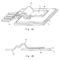
- Figs. 4A and 4B illustrate the case of using a ribbon-like connecting member
- Figs. 5A and 5B illustrate the case of using a wire
- Figs. 4A and 4B are a perspective view and a cross-sectional view, respectively.
- This embodiment uses a ribbon-like connecting member 15 for the connection between the lead frame 14 and the electrodes on the semiconductor chip 3. Specifically, one end of the lead frame 14 and one end of the ribbon-like connecting member 15 are electrically connected, and the other end of the ribbon-like connecting member 15 and the electrodes 3a and 3b of the semiconductor chip 3 are electrically connected.
- the connection of the ribbon-like connecting member 15 with the semiconductor chip 3 and the lead frame 14 is made by the laser welding.
- the ribbon-like connecting member 15 is thinner than the lead frame 14, and a thickness ratio of the ribbon-like connecting member 15 with respect to the electrodes 3a and 3b of the semiconductor chip 3 is set to 30 or lower, or preferably 5 to 30.
- the lead frame 14 is thicker than the ribbon-like connecting member 15, and a thickness ratio of the lead frame 14 with respect to the ribbon-like connecting member 15 is set to 30 or lower for stable laser welding. In the laser welding between the lead frame 14 and the ribbon-like connecting member 15, the thickness ratio is not necessarily 30 or lower because there is no risk of damaging a lower-layer element.
- Figs. 5A and 5B are a top view and a cross-sectional view, respectively. They show the case of using a wire 25 for the connection of the lead frame 14 and the electrodes of the semiconductor chip 3. As shown in Figs. 5A and 5B, the lead frame 14 and a connecting portion 25b formed at one end of the wire 25 are electrically connected, and a connecting portion 25a formed at the other end of the wire 25 and the electrodes of the semiconductor chip 3 are electrically connected.
- the wire 25 normally has a circular cross section, the ends (connecting portions 25a and 25b) of the wire 25 are thin-plate shaped in this embodiment for the laser welding with the lead frame 14 and the electrodes, respectively.
- a thickness ratio of the flat-plate connecting portion 25a of the wire 25 and the electrodes 3a and 3b is preferably within the range of 5 to 30 for the same reasons as described above.
- the connecting portion 25b to be welded with the lead frame 14 is also preferably shaped into a flat plate for easier laser welding.
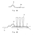
- Fig. 6 illustrates such a case.
- Fig. 6A shows the connecting portion after dimpling
- Fig. 6B shows the process of laser welding using the dimples.
- a dimple 35a is formed at one end of the connecting member 35 to serve as a connecting portion by molding or the like.
- the dimple 35a is thinner than the other part, which allows optimization of the thickness ratio with the electrodes 3a and 3b. The same effect is obtained when the dimple 35a and the electrodes on the semiconductor chip 3 are welded by laser 10.
- the dimpling is performed on the connecting member 35 to form the dimple 35a in this example, the dimpling may be performed to make connection between the lead frame 14 and the semiconductor chip 3. Specifically, the dimpling may be performed at one end of the lead frame 14 to be connected with the semiconductor chip 3 so as to form a dimple to serve as a welding area.
- the connecting area of the connecting portion 4a to become the bonding portion 5 may have an opening which is filled with metal, as a bonding material 51, that is highly absorbent of laser light.
- the bonding material 51 may be metal having higher absorbency of laser light than Cu, such as aluminum, Ni, aluminum alloy, and Ni alloy.
- the bonding material 51 and the connecting area of the connecting portion 4a contain aluminum and copper, respectively, lesser laser light power may be applied to laser-weld the bonding material 51 because a melting point of aluminum or aluminum alloy is lower than a melting point of Cu or Cu alloy.
- the bonding material 51 may be placed in the position of each bonding portion 5 to which laser light is applied as shown in Fig. 7, or may be plate-shaped to cover the positions of a plurality of bonding portions 5.
- the laser light may be applied to the bonding material 51 only or to the bonding material 51 and the surrounding connection portion 4a. If the laser light is applied to both of the bonding material 51 and the surrounding connecting portion 4a at the same time, it is possible to monitor the progress to control the laser light so as to melt the bonding material 51 without allowing the connecting portion 4a to melt. This prevents overheating of the bonding portion 5, thereby avoiding the breakdown of elements and increasing yields.
Landscapes
- Connection Of Batteries Or Terminals (AREA)
- Laser Beam Processing (AREA)
- Wire Bonding (AREA)
Abstract
Description
- The present invention relates to a manufacturing method of a semiconductor apparatus including a semiconductor chip and an electrode which is formed on the semiconductor chip and electrically connected with an external lead and, particularly, to a manufacturing method of a semiconductor apparatus capable of carrying a large current.
- Metal-Oxide-Semiconductor Field-Effect Transistors (MOSFETs), which are used for power supply in consumer-electronics products such as cell phones, personal computers, and digital audiovisual equipments or for driving a motor of vehicles, carry a high current of about 5 to 200 A. It thus requires a thick, heavy wire material. For example, a plurality of large-gauge wires of about 100 to 500 µm are connected to the source electrode of a MOSFET in order to draw a high current.
- However, the connection of a bonding wire to the source electrode by ultrasonic bonding or thermocompression bonding requires a bonding area of about 1.5 to 3 times the wire cross-sectional area. The area of the source electrode or the gate electrode, however, is limited to small and thus subject to the limitation by the wire cross-sectional area. Further, high pressure application is required to obtain a large bonding strength, and the mechanical impact causes a decrease in yields. This is described in
Japanese Unexamined Patent Application Publication No. 2002-313851 (Oono - In a semiconductor apparatus disclosed in Oono, a plate-shaped electrical path member is bonded by ultrasonic to thereby obtain a large bonding strength and achieve high yields. Fig 8 is a bird's-eye view of a semiconductor apparatus (Small Out-line Package (SOP) - 8 packages) taught by Oono. Figs. 9A and 9B are cross sectional views along lines IVA-IVA and IVB-IVB, respectively, in Fig. 8.
- Referring to Fig. 8, the
MOSFET 101 is almost entirely fixed and covered by a sealing resin (molding resin) 102 which is made of epoxy resin or the like. TheMOSFET 101 has eightleads 103, such that one end of eachlead 103 is exposed outside themolding resin 102. - Referring then to Fig. 9A, the
molding resin 102 includes a semiconductor device (semiconductor chip) 105. On thesemiconductor device 105, a source electrode (source pad) 104s and a gate electrode (gate pad) 104g are formed on the top surface, and a drain electrode (drain pad), though not shown, is formed at the end of the under surface. - Four terminals arranged on one side out of the terminals of the eight
leads 103 are integrated into one set inside themolding resin 102. The four terminals serve as drain-side terminals 103d of theleads 103 which are to be electrically connected with the drain pad. The remaining four terminals out of the terminals of the eightleads 103 are arranged so as to avoid direct contact with thesemiconductor device 105 and to be electrically disconnected from the drain-side terminals 103d and thelead 103 including a drain-side post 107d inside themolding resin 102 as shown in Fig. 9A. Out of the remaining four terminals of theleads 103, three terminals are integrated into one set, and the remaining one terminal is electrically disconnected from those three-in-one terminals of thelead 103. - The thee-in-one terminals of the
lead 103 are electrically connected with thesource electrode 104s of thesemiconductor device 105 by acurrent path member 106 to serve as source-side terminals 103s of theleads 103. The remaining one terminal of thelead 103 is electrically connected with thegate electrode 104g of thesemiconductor device 105 by asingle bonding wire 108 to serve as a gate-side terminal 103g of thelead 103. - Referring to Figs. 9A and 9B, in the
current path member 106, an electrode-side connecting portion 106a which is formed at one end is connected by plane with thesource electrode 104s, and a lead-side connecting portion 106b which is formed at the other end is connected by plane with a source-side post 107s. Thecurrent path member 106 is directly connected to both thesource electrode 104s and the source-side post 107s of each source-side terminal 103s of theleads 103 at the same time by ultrasonic bonding. - With the
current path member 106, thesemiconductor apparatus 101 taught by Oono allows the cross sectional area of the current path flowing between thesource electrode 104s of thesemiconductor device 105 and the source-side post 107s of each source-side terminal 103s of theleads 103 to be significantly larger than a total of the cross sectional area of the current path flowing through a plurality of bonding wires in a conventional MOSFET. This enables theMOSFET 101 to have significantly lower resistance between the source electrode 104c and thelead 103 compared with a conventional MOSFET. - As a different bonding technique from the ultrasonic bonding, there is laser bonding which uses laser as disclosed in Japanese Unexamined Patent Application Publication No.l-310547 (Iino), for example. Further,
Japanese Unexamined Patent Application Publication No. 6-244230 (Uemura et al. - However, the ultrasonic bonding described in Oono and Uemura et al. cause damages to products because it is a mechanical bonding technique and also cause oxidation of wires (connecting member) or electrodes because it uses heat.
- The bonding process may be carried out at the temperature of about 300°C, for example, so that an oxide film is formed on metal. Further, the temperature in the bonding process is low compared with the melting point of a metal such as a wire member, which is 800°C to 1100°C. Thus, a mechanical energy is required in order to break the oxide film formed on a wire member and to enable bonding with the low temperature in the bonding process between the electrode and the wire material. In such a case, mechanical vibration is applied so as to break the oxide film and expose a new surface, which cause damage to the chip. Particularly, a MOSFET has an active cell below the pad, and the damage caused by the ultrasonic vibration can reach the element below the pad, which leads to breakdown of a product. Further, because the process forms an alloy by mechanical contact, the bonding is not appropriate for some types of metal.
- Further, the technique of laser bonding can cause damage to a base below the electrode. As described above, large-gauge wires of about 100 to 500 µm or above are used to reduce the resistance in order for the MOSFET to carry a high current. This corresponds to the thickness of 100 to 500 µm. On the other hand, the thickness of the electrode to be connected is as small as about 2 to 6 µm as described in Oono. The adjustment of laser intensity is extremely difficult when laser-welding the members having different thicknesses, and it is impossible to provide bonding by the laser welding. High laser intensity to fuse the wire causes breakdown of the base, and low laser intensity fails to establish connection or obtain desired connection intensity.
- According to one aspect of the present invention, there is provided a manufacturing method of a semiconductor apparatus including a semiconductor chip and an electrode formed on the semiconductor chip and electrically connected with an external lead. This method laser-welds the electrode with a thin-film shaped connecting area formed partly or entirely on a connecting portion electrically connected with the external lead.
- The method makes the laser welding between the semiconductor chip and the external lead through the connecting portion. It uses a thin-film shaped connecting area which is formed partly or entirely on the connecting portion, thereby enabling laser welding with an electrode which is normally significantly thinner than the connecting portion. This achieves the establishment of electrical connection without mechanical vibration.
- The present invention provides a semiconductor apparatus manufacturing method which enables an increase in productivity and yields and exhibits high electrical operability and reliability.
- The above and other objects, advantages and features of the present invention will be more apparent from the following description taken in conjunction with the accompanying drawings, in which:
- Fig. 1A is a perspective view of a semiconductor apparatus according to an embodiment of the present invention;
- Figs. 1B and 1C are cross-sectional views along line IB-IB in Fig. 1A;
- Fig. 2 is a cross-sectional view along line II-II in Fig. 1A, showing a semiconductor apparatus according to the embodiment of the present invention;
- Figs. 3A and 3B are views to describe a semiconductor apparatus manufacturing method according to the embodiment of the present invention;
- Figs. 4A and 4B are views showing another example of a semiconductor apparatus according to the embodiment of the present invention, which are a perspective view and a cross-sectional view when using a ribbon-like connecting member, respectively;
- Figs. 5A and 5B are views showing another example of a semiconductor apparatus according to the embodiment of the present invention, which are a perspective view and a cross-sectional view when using a wire, respectively;
- Figs. 6A and 6B are a view showing a connecting portion after dimpling and a view showing the step of laser welding using the connecting portion after dimpling, respectively;
- Fig. 7 is a view showing a lead frame in another example of a semiconductor apparatus according to the embodiment of the present invention;
- Fig. 8 is a bird's-eye view of a semiconductor apparatus (Small Out-line Package (SOP) - 8 packages) disclosed in Oono; and
- Figs. 9A and 9B are cross sectional views along lines IVA-IVA and IVB-IVB, respectively, in Fig. 7, showing the semiconductor apparatus disclosed in Oono.
- The invention will be now described herein with reference to illustrative embodiments. Those skilled in the art will recognize that many alternative embodiments can be accomplished using the teachings of the present invention and that the invention is not limited to the embodiments illustrated for explanatory purposed.
- An exemplary embodiment of the present invention is described hereinafter in detail with reference to the drawings. In the below-described embodiment, the present invention is applied to a semiconductor apparatus for carrying a high current which is used for power supply or switches in cell phones, motors and so on, in which a number of MOSFETs are combined into one MOSFET. While a single transistor normally carries a current of about 0.1A, such a transistor can carry a current of about 5 to 200A and can be used for power supply in consumer-electronics products, motor driving in vehicles or the like.
- Fig. 1A is a perspective view of a semiconductor apparatus according to an embodiment of the present invention. Figs. 1B and 1C are cross-sectional views along line IB-IB in Fig. 1A. As shown in Figs. 1A and 1B, a
semiconductor apparatus 1 includes a die pad (island) 2 formed on a lead frame, a semiconductor chip (die) 3 which is mounted on thedie pad 2, and alead frame 4 which is electrically connected with thesemiconductor chip 3. Typically, these elements are covered with a molding resin made of epoxy resin or the like and packaged entirely except for one end (outer lead (external lead) 4b) of thelead frame 4. - The
lead frame 4 includes a portion for mounting the semiconductor chip 3 (which is referred to as the die pad or the internal lead) and a portion projecting outside of the package and soldered to a substrate (which is referred to as the external lead) . Because a different feature is required for each portion, the die pad and the internal lead may be nickel-plated or non-plated, and the external lead may be solder- or tin- plated, for example. - The
semiconductor chip 3 may be formed of a vertical MOSFET, for example. A drain electrode, though not shown, is formed on its under surface and connected to thedie pad 2. An external lead, also not shown, which is connected with thedie pad 2 serves as a drain-side terminal. On the upper surface of thesemiconductor chip 3 are formed a source electrode (electrode pad) 3a and a gate electrode (electrode pad) 3b. A connectingportion 4a having a thin-film shape (flat-plate or ribbon-like shape) which is formed at the end of the internal lead of thelead frame 4 is electrically connected with thesource electrode 3a and thegate electrode 3b. In thesemiconductor apparatus 1 illustrated in Fig. 1B, thelead frame 4 is not plated. In asemiconductor apparatus 40 illustrated in Fig. 1C, on the other hand, thelead frame 4 includes a base 41 such as Cu and aplating layer 42 such as Ni which is formed on thebase 41. - In the
semiconductor apparatus 1 according to this embodiment, the connectingportion 4a of thelead frame 4 is bonded by laser welding with thesource electrode 3a and thegate electrode 3b, and one or a plurality of weld-bonding portions 5 are provided depending on the bonding area. The use of laser welding for connection facilitates the positioning between thelead frame 4 and thesemiconductor chip 3 and thus enables easier manufacturing such as one-time connection using a galvanometer mirror or the like. - As described earlier, the connecting member such as the internal lead or the wire and the electrodes on the
semiconductor chip 3 cannot be laser-welded simply. While the thickness of the electrode on thesemiconductor chip 3 is typically about 4 to 5 µm, the thickness of the connecting member such the wire is about several tens to hundreds times greater. If a thickness ratio of the members to be welded differs largely, the use of high laser power with the intent to weld those members can result in breakdown of the base underneath. On the other hand, the use of low laser power fails to establish connection or obtain desired connection intensity. Thus, the breakdown of the elements below the electrode can occur unless optimizing the thickness of the connecting portion with respect to the thickness of the electrode. - On the other hand, the technique of using the ribbon-like or flat-plate connecting member and performing the ultrasonic bonding as disclosed in Oono causes the element to be subject to breakdown due to the mechanical vibration, and the ultrasonic bonding of a large area requires a large-scale machine to increase manufacturing costs.
- The inventor of the present invention has found that a connecting member and electrodes on the
semiconductor chip 3 can be laser-welded by forming at least a part of the connecting member to be electrically connected with the electrode, which is referred to hereinafter as the connecting portion, into a thin-film shape (flat-plate or ribbon-like shape) and minimizing a difference (ratio) in thickness between the connecting portion and the electrodes. Accordingly, thelead frame 4 of this embodiment has the connectingportion 4a having a thin-film shape which is thinner than the other part. The laser welding is applied between the connectingportion 4a and theelectrodes portion 4a is not necessarily entirely thin-film shaped. The laser welding is possible with equal effect as long as at least an area to be laser-welded, which is a part of the connectingportion 4a, is thin-film shaped to serve as a welding area. - Specifically, the inventor of the present invention has found that suitable connection intensity can be obtained by laser welding without damaging the base below the electrodes by setting the thickness of the connecting
portion 4a to be less than thirty times the thickness of theelectrodes semiconductor chip 3. The thickness of the connectingportion 4a is preferably 5 to 30 times, more preferably 10 to 20 times, the thickness of theelectrodes - As described earlier, when using laser welding, it is preferred to set an appropriate thickness ratio between the connecting
portion 4a and theelectrodes portion 4a is more than thirty times the thickness of theelectrodes portion 4a can cause the laser to penetrate through thethin electrodes - Although it is ideal for the laser welding to equalize the thickness of the electrodes and the thickness of the connecting
portion 4a, if the thickness of the connectingportion 4a is less than 5 times the thickness of theelectrodes portion 4a, which is not practical, Thus, the thickness of the connectingportion 4a is preferably equal to or more than 5 times the thickness of theelectrodes electrodes portion 4a of thelead frame 4 is preferably about 25 to 150 µm. - Further, it is preferred to determine the contact area of the connecting
portion 4a with theelectrodes portion 4a and the current flowing through theelectrodes portion 4a and theelectrodes - As described above, the semiconductor apparatus according to this embodiment may carry a current of 5 to 200 A, and it is preferred to design the sizes of the connecting
portion 4a and theelectrodes portion 4a is actually in contact with theelectrodes portion 4a. Specifically, the connectingportion 4a is laser-welded at a plurality of points, and the part surrounded by the outermost weld-bonding portions 5 serves as the contact area. - The electrical resistance of the contacting
portion 4a is preferably low for smaller current loss. However, because the semiconductor apparatus (MOSFET) 1 controls ON/OFF of a switch by a prescribed resistance value, the resistance to enable the switching function is required at least. It is thus preferred to determine the thickness of the connectingportion 4a and the contact area based on the resistance value necessary to serve as a switch. - The area of the connecting
portion 4a may be larger than the area of theelectrodes electrode 3a is formed on thesemiconductor chip 3 which is mounted on thedie pad 2. Anonconductive cover layer 6 which may be made of polymide (PI), phosphate glass (PSG), an oxide film or the like is formed in the vicinity of theelectrode 3a to cover the elements around theelectrode 3a. This prevents the connectingportion 4a from being electrically continuous with other elements even if the connectingportion 4a is larger than the actual area of theelectrode 3a. This further facilitates the positioning between the connectingportion 4a and theelectrodes portion 4a being large. - Because the part of the connecting
portion 4a which extends off theelectrodes cover material 6, no electrical continuity is established when the contactingportion 4a contacts the elements in the vicinity of theelectrode 3a. Although a sight gap can be present between the connectingportion 4a and theelectrode 3a in this case, the connectingportion 4a and theelectrode 3a are fused by the laser welding into abonding portion 5 to thereby allow them to be electrically bonded. Fig. 2 schematically illustrates that. - The connecting
portion 4a (lead frame 4) is typically formed of aluminum, copper, or an alloy of those. The use of gold, silver, palladium, or an alloy of those is also possible. Further, a metal material may be formed on the surface of such a connecting member. - The copper is particularly suitable for use as a connecting member because of its high conductivity; however, it has low laser absorbency. Therefore, for easier laser welding, it is possible to provide the plating of nickel (Ni) having high laser absorbency on the surface of copper or form an alloy of Ni and copper.
- In a MOSFET, for example, a gate electrode is formed below a source electrode (lead electrode) with an insulating film interposed therebetween. The insulating film may be formed of oxide silicon glass (BPSG: borophosphorous silicate glass) added with phosphorous and boron, PSG (phosphorous silicate glass) or the like. If damage is applied to the insulating film by laser welding, the MOSFET becomes inoperable. It is therefore preferred that the insulating film as the base is formed of a heat resistant material.
- When using the
lead frame 4 as a connecting material, a beam to bridge thelead frame 4 and theelectrodes portion 4a) may be adjusted appropriately according to the chip size. - It the
lead frame 4 and theelectrodes - If the connecting
portion 4a and theelectrodes portion 4a and theelectrodes - Further, the laser welding fuses the metal of the connecting
portion 4a of thelead frame 4 and theelectrodes - Furthermore, the bonding by the laser welding does not apply any mechanical stress, thus not causing damage to the
semiconductor chip 3 to thereby increase yields. In addition, because the laser welding is a normal temperature process in which heat is generated only in the welding portion, it does not cause oxidation of thelead frame 4 or thesemiconductor chip 3. - A manufacturing method of the semiconductor apparatus according to this embodiment is described hereinafter. This embodiment uses an external lead (lead frame) 4 whose end is shaped into the thin-
film connecting portion 4a. Thelead frame 4 of such a shape can be obtained by forming the thin-film shaped connectingportion 4a simultaneously during molding. This enables the formation of thelead frame 4 with the thin-film shaped connectingportion 4a to enable laser welding without any additional step. The connectingportion 4a is formed at the end of thelead frame 4 so as to have a given thickness and the size and shape according to theelectrodes semiconductor chip 3. - Then, the
semiconductor chip 3 is mounted on thedie pad 2. Thedie pad 2 and thesemiconductor chip 3 may be electrically connected by soldering, silver paste, or the like. Thelead frame 4 is placed thereon so that the connectingportion 4a of thelead frame 4 and theelectrodes semiconductor chip 3 are placed on one another. As described above, the positioning accuracy may be about ±100 µm because they are to be bonded by laser welding. - Referring now to Figs. 3A and 3B, laser is applied to partly fuse the connecting
portion 4a of thelead frame 4 and theelectrodes portion 4a and thesource electrode 3a may be welded at a plurality of positions with a prescribed interval because theelectrode 3a is large. - The use of a galvanometer for the laser welding enables one-time connection to enhance the productivity. The
semiconductor chip 3 and thelead frame 4 can be connected easily as described above. - The connection between the
lead frame 4 and theelectrodes lead frame 4 which is processed as above. Alternatively, thelead frame 4 and theelectrodes - Figs. 4A and 4B illustrate the case of using a ribbon-like connecting member, and Figs. 5A and 5B illustrate the case of using a wire. Figs. 4A and 4B are a perspective view and a cross-sectional view, respectively. In the following description, the same elements as in Figs. 1 and 2 are denoted by the same reference numerals and not described in detail herein. This embodiment uses a ribbon-like connecting
member 15 for the connection between thelead frame 14 and the electrodes on thesemiconductor chip 3. Specifically, one end of thelead frame 14 and one end of the ribbon-like connectingmember 15 are electrically connected, and the other end of the ribbon-like connectingmember 15 and theelectrodes semiconductor chip 3 are electrically connected. The connection of the ribbon-like connectingmember 15 with thesemiconductor chip 3 and thelead frame 14 is made by the laser welding. The ribbon-like connectingmember 15 is thinner than thelead frame 14, and a thickness ratio of the ribbon-like connectingmember 15 with respect to theelectrodes semiconductor chip 3 is set to 30 or lower, or preferably 5 to 30. Thelead frame 14 is thicker than the ribbon-like connectingmember 15, and a thickness ratio of thelead frame 14 with respect to the ribbon-like connectingmember 15 is set to 30 or lower for stable laser welding. In the laser welding between thelead frame 14 and the ribbon-like connectingmember 15, the thickness ratio is not necessarily 30 or lower because there is no risk of damaging a lower-layer element. - Figs. 5A and 5B are a top view and a cross-sectional view, respectively. They show the case of using a
wire 25 for the connection of thelead frame 14 and the electrodes of thesemiconductor chip 3. As shown in Figs. 5A and 5B, thelead frame 14 and a connectingportion 25b formed at one end of thewire 25 are electrically connected, and a connectingportion 25a formed at the other end of thewire 25 and the electrodes of thesemiconductor chip 3 are electrically connected. Although thewire 25 normally has a circular cross section, the ends (connectingportions wire 25 are thin-plate shaped in this embodiment for the laser welding with thelead frame 14 and the electrodes, respectively. - In this case also, a thickness ratio of the flat-
plate connecting portion 25a of thewire 25 and theelectrodes portion 25b to be welded with thelead frame 14 is also preferably shaped into a flat plate for easier laser welding. - As described above, it is possible to perform laser welding with the electrodes on the semiconductor chip by forming a thin-film connecting area in a part of the connecting portion. Fig. 6 illustrates such a case. Fig. 6A shows the connecting portion after dimpling, and Fig. 6B shows the process of laser welding using the dimples.
- As shown in Figs. 6A and 6B, a
dimple 35a is formed at one end of the connectingmember 35 to serve as a connecting portion by molding or the like. Thedimple 35a is thinner than the other part, which allows optimization of the thickness ratio with theelectrodes dimple 35a and the electrodes on thesemiconductor chip 3 are welded bylaser 10. Although the dimpling is performed on the connectingmember 35 to form thedimple 35a in this example, the dimpling may be performed to make connection between thelead frame 14 and thesemiconductor chip 3. Specifically, the dimpling may be performed at one end of thelead frame 14 to be connected with thesemiconductor chip 3 so as to form a dimple to serve as a welding area. - Further, as a
semiconductor apparatus 50 shown in Fig. 7, the connecting area of the connectingportion 4a to become thebonding portion 5 may have an opening which is filled with metal, as abonding material 51, that is highly absorbent of laser light. For example, if the connectingportion 4a (lead frame 4) is made of Cu, thebonding material 51 may be metal having higher absorbency of laser light than Cu, such as aluminum, Ni, aluminum alloy, and Ni alloy. Expressly thebonding material 51 and the connecting area of the connectingportion 4a contain aluminum and copper, respectively, lesser laser light power may be applied to laser-weld thebonding material 51 because a melting point of aluminum or aluminum alloy is lower than a melting point of Cu or Cu alloy. Thebonding material 51 may be placed in the position of eachbonding portion 5 to which laser light is applied as shown in Fig. 7, or may be plate-shaped to cover the positions of a plurality ofbonding portions 5. - When applying laser light to the
bonding material 51, the laser light may be applied to thebonding material 51 only or to thebonding material 51 and the surroundingconnection portion 4a. If the laser light is applied to both of thebonding material 51 and the surrounding connectingportion 4a at the same time, it is possible to monitor the progress to control the laser light so as to melt thebonding material 51 without allowing the connectingportion 4a to melt. This prevents overheating of thebonding portion 5, thereby avoiding the breakdown of elements and increasing yields. - It is apparent that the present invention is not limited to the above embodiment that may be modified and changed without departing from the scope and spirit of the invention.
Claims (19)
- A manufacturing method of a semiconductor apparatus, comprising:forming a thin-film shaped connecting area on a connecting portion (4a) electrically connected with an external lead (4); andwelding the connecting area of the connecting portion (4a) and an electrode (3a) on a semiconductor chip (3) by laser welding.
- The manufacturing method of a semiconductor apparatus according to claim 1, wherein a thickness ratio of the connecting area with respect to the electrode (3a) is in a range of 5 to 30.
- The manufacturing method of a semiconductor apparatus according to claim 2, wherein a contact area of the connecting portion (4a) with the electrode (3a) is determined based on a thickness of the connecting portion (4a) and desired current and resistance values.
- The manufacturing method of a semiconductor apparatus according to claim 1, wherein the external lead (4) includes the connecting portion (4a) at one end of the external lead (4).
- The manufacturing method of a semiconductor apparatus according to claim 1, wherein a wire (25) having at one end a connecting portion (25a) including the connecting area is used as a connecting member to electrically connect with an external lead (14) by laser-welding the connecting portion (25a) of the wire (25) and the electrode (3a).
- The manufacturing method of a semiconductor apparatus according to claim 1, wherein a thin-film conductive ribbon (15) is used as a connecting member to electrically connect with an external lead (14) by laser-welding the connecting portion (4a) of the thin-film conductive ribbon (15) and the electrode (3a).
- The manufacturing method of a semiconductor apparatus according to one of claims 1-5, wherein the connecting portion (4a) includes a dimple (35a) in the connecting area, and the dimple (35a) is laser-welded for connecting the connecting portion (4a) and the electrode (3a).
- The manufacturing method of a semiconductor apparatus according to one of claims 5-7, wherein another end of the connecting member and the external lead (4) are laser-welded.
- The manufacturing method of a semiconductor apparatus according to one of claims 1-8, further comprising:a nonconductive cover layer (6) in close proximity to the electrode (3a),wherein an area of the connecting portion (4a) is larger than an exposed area of the electrode (3a) from the nonconductive cover layer (6).
- The manufacturing method of a semiconductor apparatus according to one of claims 1-8, wherein laser-welding is performed by applying laser light (10) to a plurality of positions on the connecting portion (4a).
- The manufacturing method of a semiconductor apparatus according to one of claims 1-8, wherein the electrode (3a) is formed of a metal containing at least one of aluminum and copper.
- The manufacturing method of a semiconductor apparatus according to one of claims 1-8, wherein the connecting portion (4a) is made of a material containing at least one metal selected from the group consisting of aluminum, copper, gold, silver, palladium and nickel.
- The manufacturing method of a semiconductor apparatus according to one of claims 1-8, wherein the connecting portion (4a) is formed of nickel-plated copper or copper alloy.
- The manufacturing method of a semiconductor apparatus according to claim 1, comprising:an opening formed in the connecting area of the connecting portion (4a), anda bonding material (51) filled in the opening in the connecting area of the connecting portion (4a),wherein laser light is applied to an area including the bonding material (51) to laser-weld the bonding material and the electrode (3a).
- The manufacturing method of a semiconductor apparatus according to claim 14, wherein
a melting point of the bonding material (51) is lower than a melting point of a material of the connecting area of the connecting portion (4a). - The manufacturing method of a semiconductor apparatus according to claim 14, wherein
the bonding material (51) contains aluminum and the material of the connecting area of the connecting portion (4a) contains copper. - The manufacturing method of a semiconductor apparatus according to claim 1, wherein
the semiconductor chip (3) is mounted on a die pad (2) of a first lead frame, and
the external lead (4) is formed on a second lead frame different from the first lead frame. - The manufacturing method of a semiconductor apparatus according to claim 18, wherein
the semiconductor chip (3) includes a transistor including a gate electrode (3a) and a source electrode (3a) on a top surface and a drain electrode on a bottom surface,
a drain lead is integrated with the die pad (2), and
the external lead (4) includes a source lead electrically connected with the source electrode (3a). - The manufacturing method of a semiconductor apparatus according to claim 18, wherein the transistor includes a metal-oxide-semiconductor (MOS) transistor.
Applications Claiming Priority (2)
| Application Number | Priority Date | Filing Date | Title |
|---|---|---|---|
| JP2006015505 | 2006-01-24 | ||
| JP2006351653A JP4842118B2 (en) | 2006-01-24 | 2006-12-27 | Manufacturing method of semiconductor device |
Publications (2)
| Publication Number | Publication Date |
|---|---|
| EP1811557A2 true EP1811557A2 (en) | 2007-07-25 |
| EP1811557A3 EP1811557A3 (en) | 2007-10-10 |
Family
ID=37907395
Family Applications (1)
| Application Number | Title | Priority Date | Filing Date |
|---|---|---|---|
| EP07000718A Withdrawn EP1811557A3 (en) | 2006-01-24 | 2007-01-15 | Semiconductor apparatus manufacturing method |
Country Status (4)
| Country | Link |
|---|---|
| US (1) | US7772031B2 (en) |
| EP (1) | EP1811557A3 (en) |
| JP (1) | JP4842118B2 (en) |
| CN (1) | CN101009235B (en) |
Cited By (7)
| Publication number | Priority date | Publication date | Assignee | Title |
|---|---|---|---|---|
| GB2451077A (en) * | 2007-07-17 | 2009-01-21 | Zetex Semiconductors Plc | Semiconductor chip package |
| EP2743973A3 (en) * | 2012-12-11 | 2014-12-03 | Robert Bosch Gmbh | Method for contacting a semiconductor element by welding a contact element to a sintered layer on the semiconductor element and semiconductor component with increased stability against thermomechanical influence |
| DE102016204150A1 (en) * | 2016-03-14 | 2017-09-14 | Siemens Aktiengesellschaft | Method, semiconductor module, power converter and vehicle |
| CN109003909A (en) * | 2017-06-07 | 2018-12-14 | 三菱电机株式会社 | The manufacturing method of semiconductor device |
| WO2020212031A1 (en) * | 2019-04-18 | 2020-10-22 | Abb Power Grids Switzerland Ag | Power semiconductor module with laser-welded leadframe |
| WO2021239321A1 (en) * | 2020-05-28 | 2021-12-02 | Siemens Aktiengesellschaft | Method for welding an attachment piece to a semiconductor metallisation by laser welding, and electronics module |
| DE102020208440A1 (en) | 2020-07-06 | 2022-01-27 | Zf Friedrichshafen Ag | Method of manufacturing a half-bridge module, half-bridge module and inverter |
Families Citing this family (29)
| Publication number | Priority date | Publication date | Assignee | Title |
|---|---|---|---|---|
| JP4248953B2 (en) | 2003-06-30 | 2009-04-02 | 株式会社ルネサステクノロジ | Semiconductor device and manufacturing method thereof |
| DE102006017115B4 (en) * | 2006-04-10 | 2008-08-28 | Infineon Technologies Ag | Semiconductor device with a plastic housing and method for its production |
| JP2008294384A (en) * | 2007-04-27 | 2008-12-04 | Renesas Technology Corp | Semiconductor device |
| CN101933139B (en) | 2007-12-20 | 2012-11-07 | 爱信艾达株式会社 | Semiconductor device and method for fabricating the same |
| JP2009194153A (en) * | 2008-02-14 | 2009-08-27 | Toshiba Corp | Semiconductor device manufacturing method and ultrasonic bonding apparatus |
| JP4978570B2 (en) * | 2008-06-12 | 2012-07-18 | 株式会社デンソー | Laser welding method |
| CN101673722A (en) * | 2008-09-10 | 2010-03-17 | 日月光半导体制造股份有限公司 | Lead frame |
| JP2010118577A (en) * | 2008-11-14 | 2010-05-27 | Sumitomo Electric Ind Ltd | Resin encapsulated semiconductor device and method of manufacturing the same |
| US8513110B2 (en) * | 2009-06-14 | 2013-08-20 | Jayna Sheats | Processes and structures for beveled slope integrated circuits for interconnect fabrication |
| CA2766240A1 (en) * | 2009-06-23 | 2010-12-29 | Toshiba Mitsubishi-Electric Industrial Systems Corporation | Electrode base |
| JP2011216518A (en) * | 2010-03-31 | 2011-10-27 | Rohm Co Ltd | Wire bonding structure, semiconductor device, bonding tool, and wire bonding method |
| CN102049580B (en) * | 2010-09-26 | 2013-04-24 | 广州金升阳科技有限公司 | Welding method of lead frame |
| DE102011088418B4 (en) | 2011-12-13 | 2023-06-22 | Robert Bosch Gmbh | bond connection |
| JP2013143519A (en) * | 2012-01-12 | 2013-07-22 | Fuji Electric Co Ltd | Connector and resin sealed type semiconductor device |
| JP2014012284A (en) * | 2012-07-04 | 2014-01-23 | Toyota Motor Corp | Heating method, and joining method |
| US9437756B2 (en) | 2013-09-27 | 2016-09-06 | Sunpower Corporation | Metallization of solar cells using metal foils |
| DE102014116283B4 (en) * | 2014-11-07 | 2016-05-19 | Webasto SE | Method for processing a first component and a second component and device |
| DE102015119252B4 (en) | 2015-11-09 | 2024-02-01 | Webasto SE | Device for a heater for a vehicle |
| WO2017208941A1 (en) * | 2016-06-01 | 2017-12-07 | 三菱電機株式会社 | Semiconductor device and method for manufacturing same |
| US9754864B1 (en) * | 2016-06-23 | 2017-09-05 | Alpha And Omega Semiconductor Incorporated | Semiconductor power device having single in-line lead module and method of making the same |
| US10431545B2 (en) * | 2017-06-29 | 2019-10-01 | Intel IP Corporation | Cross-connected multi-chip modules coupled by silicon bent-bridge interconnects and methods of assembling same |
| WO2019077866A1 (en) * | 2017-10-19 | 2019-04-25 | 富士電機株式会社 | Semiconductor device and semiconductor device production method |
| JP6945418B2 (en) | 2017-10-24 | 2021-10-06 | 三菱電機株式会社 | Semiconductor devices and manufacturing methods for semiconductor devices |
| CN111933606B (en) * | 2020-09-16 | 2021-08-03 | 苏州日月新半导体有限公司 | Integrated circuit device and packaging method thereof |
| JP7643186B2 (en) * | 2021-05-31 | 2025-03-11 | 富士電機株式会社 | Semiconductor module and method for manufacturing the same |
| JP7574753B2 (en) * | 2021-07-05 | 2024-10-29 | 三菱電機株式会社 | Semiconductor device and method for manufacturing the same |
| KR102840683B1 (en) | 2022-11-30 | 2025-07-31 | 한국생산기술연구원 | Bonding Material Laser Soldering Method using Hole drilling pattern and Bonding structure thereof |
| CN119368916A (en) * | 2023-07-26 | 2025-01-28 | 中国科学院半导体研究所 | Welding method for ultra-thin metal electrode connection |
| DE102024105616A1 (en) * | 2024-02-28 | 2025-08-28 | Semikron Danfoss Elektronik Gmbh & Co. Kg | Arrangement with a printed circuit board and a power electronic component and method for manufacturing |
Family Cites Families (22)
| Publication number | Priority date | Publication date | Assignee | Title |
|---|---|---|---|---|
| US4845335A (en) | 1988-01-28 | 1989-07-04 | Microelectronics And Computer Technology Corporation | Laser Bonding apparatus and method |
| JPH01310547A (en) | 1988-06-08 | 1989-12-14 | Nec Corp | Bonding of semiconductor device |
| US5164566A (en) | 1990-06-12 | 1992-11-17 | Microelectronics And Computer Technology Corp. | Method and apparatus for fluxless solder reflow |
| US5306891A (en) | 1992-04-02 | 1994-04-26 | Motorola, Inc. | Laser welding process for attaching metal to ceramic substrate |
| JPH06244230A (en) | 1993-02-16 | 1994-09-02 | Nippondenso Co Ltd | Device having bonding electrode and method of manufacturing bonding electrode |
| JP2783125B2 (en) | 1993-07-23 | 1998-08-06 | 株式会社デンソー | Wire bonding method |
| JPH07273267A (en) * | 1994-03-31 | 1995-10-20 | Toppan Printing Co Ltd | Lead joining method |
| JP3459054B2 (en) * | 1995-04-26 | 2003-10-20 | ローム株式会社 | Manufacturing method of semiconductor devices |
| US5731244A (en) * | 1996-05-28 | 1998-03-24 | Micron Technology, Inc. | Laser wire bonding for wire embedded dielectrics to integrated circuits |
| US6006981A (en) * | 1996-11-19 | 1999-12-28 | Texas Instruments Incorporated | Wirefilm bonding for electronic component interconnection |
| JPH10334962A (en) * | 1997-06-03 | 1998-12-18 | Harness Sogo Gijutsu Kenkyusho:Kk | Laser welding structure |
| JP3547953B2 (en) * | 1997-09-30 | 2004-07-28 | 三洋電機株式会社 | Manufacturing method of cylindrical non-aqueous electrolyte secondary battery |
| JPH11215652A (en) * | 1998-01-23 | 1999-08-06 | Harness Syst Tech Res Ltd | Laser welding structure of bus-bar |
| JP2000141029A (en) * | 1998-11-04 | 2000-05-23 | Harness Syst Tech Res Ltd | Connection method by laser |
| KR20000057810A (en) * | 1999-01-28 | 2000-09-25 | 가나이 쓰토무 | Semiconductor device |
| JP2001068171A (en) * | 1999-08-30 | 2001-03-16 | Sumitomo Wiring Syst Ltd | Circuit conductor jointing structure of junction block |
| JP4102012B2 (en) * | 2000-09-21 | 2008-06-18 | 株式会社東芝 | Semiconductor device manufacturing method and semiconductor device |
| US6801174B2 (en) * | 2000-12-04 | 2004-10-05 | Sony Corporation | Display device, producing method of electronic apparatus and display device |
| JP3898459B2 (en) | 2001-04-18 | 2007-03-28 | 加賀東芝エレクトロニクス株式会社 | Manufacturing method of semiconductor device |
| SE521528C3 (en) | 2001-08-07 | 2003-12-10 | Ericsson Telefon Ab L M | Welded leg frame |
| JP2004281887A (en) * | 2003-03-18 | 2004-10-07 | Himeji Toshiba Ep Corp | Lead frame and electronic component using the same |
| JP3739091B2 (en) * | 2003-04-03 | 2006-01-25 | 株式会社東芝 | Manufacturing method of semiconductor device |
-
2006
- 2006-12-27 JP JP2006351653A patent/JP4842118B2/en not_active Expired - Fee Related
-
2007
- 2007-01-08 US US11/650,495 patent/US7772031B2/en not_active Expired - Fee Related
- 2007-01-15 EP EP07000718A patent/EP1811557A3/en not_active Withdrawn
- 2007-01-23 CN CN2007100040992A patent/CN101009235B/en not_active Expired - Fee Related
Cited By (9)
| Publication number | Priority date | Publication date | Assignee | Title |
|---|---|---|---|---|
| GB2451077A (en) * | 2007-07-17 | 2009-01-21 | Zetex Semiconductors Plc | Semiconductor chip package |
| EP2743973A3 (en) * | 2012-12-11 | 2014-12-03 | Robert Bosch Gmbh | Method for contacting a semiconductor element by welding a contact element to a sintered layer on the semiconductor element and semiconductor component with increased stability against thermomechanical influence |
| DE102016204150A1 (en) * | 2016-03-14 | 2017-09-14 | Siemens Aktiengesellschaft | Method, semiconductor module, power converter and vehicle |
| CN109003909A (en) * | 2017-06-07 | 2018-12-14 | 三菱电机株式会社 | The manufacturing method of semiconductor device |
| CN109003909B (en) * | 2017-06-07 | 2023-01-06 | 三菱电机株式会社 | Manufacturing method of semiconductor device |
| WO2020212031A1 (en) * | 2019-04-18 | 2020-10-22 | Abb Power Grids Switzerland Ag | Power semiconductor module with laser-welded leadframe |
| US11749633B2 (en) | 2019-04-18 | 2023-09-05 | Hitachi Energy Switzerland Ag | Power semiconductor module with laser-welded leadframe |
| WO2021239321A1 (en) * | 2020-05-28 | 2021-12-02 | Siemens Aktiengesellschaft | Method for welding an attachment piece to a semiconductor metallisation by laser welding, and electronics module |
| DE102020208440A1 (en) | 2020-07-06 | 2022-01-27 | Zf Friedrichshafen Ag | Method of manufacturing a half-bridge module, half-bridge module and inverter |
Also Published As
| Publication number | Publication date |
|---|---|
| EP1811557A3 (en) | 2007-10-10 |
| US20070172980A1 (en) | 2007-07-26 |
| JP2007227893A (en) | 2007-09-06 |
| US7772031B2 (en) | 2010-08-10 |
| CN101009235B (en) | 2011-12-21 |
| CN101009235A (en) | 2007-08-01 |
| JP4842118B2 (en) | 2011-12-21 |
Similar Documents
| Publication | Publication Date | Title |
|---|---|---|
| US7772031B2 (en) | Semiconductor apparatus manufacturing method | |
| CN101339934B (en) | Semiconductor device with welded leads and method of manufacturing the same | |
| US7820489B2 (en) | Method of manufacturing semiconductor apparatus | |
| US8299600B2 (en) | Semiconductor device and manufacturing method thereof | |
| US20240379610A1 (en) | Semiconductor device and bonding method | |
| US9824996B2 (en) | Semiconductor device having low on resistance | |
| EP3544053B1 (en) | Discrete power transistor package having solderless dbc to leadframe attach | |
| US7868432B2 (en) | Multi-chip module for battery power control | |
| JP5176507B2 (en) | Semiconductor device | |
| US20150380344A1 (en) | Resin sealing type semiconductor device and method of manufacturing the same, and lead frame | |
| US20050023670A1 (en) | Semiconductor device and a method of manufacturing the same | |
| JP2009059923A (en) | Semiconductor device | |
| KR20130051498A (en) | Semiconductor module and method of manufacturing a semiconductor module | |
| KR20180120598A (en) | Semiconductor device and manufacturing method thereof | |
| JP2009267054A (en) | Semiconductor device and manufacturing method thereof | |
| CN105609441A (en) | Method for manufacturing semiconductor device | |
| JP2005101293A (en) | Semiconductor device | |
| JP7472806B2 (en) | Semiconductor device, power module, and method of manufacturing the semiconductor device | |
| JP2009224529A (en) | Semiconductor device and its manufacturing method | |
| CN120376535A (en) | Semiconductor device with a semiconductor device having a plurality of semiconductor chips | |
| EP0470210A1 (en) | Low inductance encapsulated package including a semiconductor chip | |
| JP2008041566A (en) | Semiconductor device and its manufacturing method |
Legal Events
| Date | Code | Title | Description |
|---|---|---|---|
| PUAI | Public reference made under article 153(3) epc to a published international application that has entered the european phase |
Free format text: ORIGINAL CODE: 0009012 |
|
| AK | Designated contracting states |
Kind code of ref document: A2 Designated state(s): AT BE BG CH CY CZ DE DK EE ES FI FR GB GR HU IE IS IT LI LT LU LV MC NL PL PT RO SE SI SK TR |
|
| AX | Request for extension of the european patent |
Extension state: AL BA HR MK YU |
|
| PUAL | Search report despatched |
Free format text: ORIGINAL CODE: 0009013 |
|
| AK | Designated contracting states |
Kind code of ref document: A3 Designated state(s): AT BE BG CH CY CZ DE DK EE ES FI FR GB GR HU IE IS IT LI LT LU LV MC NL PL PT RO SE SI SK TR |
|
| AX | Request for extension of the european patent |
Extension state: AL BA HR MK YU |
|
| STAA | Information on the status of an ep patent application or granted ep patent |
Free format text: STATUS: THE APPLICATION HAS BEEN WITHDRAWN |
|
| 18W | Application withdrawn |
Effective date: 20071026 |