US9754864B1 - Semiconductor power device having single in-line lead module and method of making the same - Google Patents
Semiconductor power device having single in-line lead module and method of making the same Download PDFInfo
- Publication number
- US9754864B1 US9754864B1 US15/191,414 US201615191414A US9754864B1 US 9754864 B1 US9754864 B1 US 9754864B1 US 201615191414 A US201615191414 A US 201615191414A US 9754864 B1 US9754864 B1 US 9754864B1
- Authority
- US
- United States
- Prior art keywords
- semiconductor chip
- clip
- top surface
- side semiconductor
- low
- Prior art date
- Legal status (The legal status is an assumption and is not a legal conclusion. Google has not performed a legal analysis and makes no representation as to the accuracy of the status listed.)
- Active
Links
- 239000004065 semiconductor Substances 0.000 title claims abstract description 124
- 238000004519 manufacturing process Methods 0.000 title description 2
- 238000005538 encapsulation Methods 0.000 claims abstract description 26
- 238000000465 moulding Methods 0.000 claims abstract description 12
- 239000000463 material Substances 0.000 claims description 18
- 238000000034 method Methods 0.000 abstract description 11
- 239000007769 metal material Substances 0.000 description 3
- 238000012986 modification Methods 0.000 description 3
- 230000004048 modification Effects 0.000 description 3
- PXHVJJICTQNCMI-UHFFFAOYSA-N Nickel Chemical compound [Ni] PXHVJJICTQNCMI-UHFFFAOYSA-N 0.000 description 2
- RYGMFSIKBFXOCR-UHFFFAOYSA-N Copper Chemical compound [Cu] RYGMFSIKBFXOCR-UHFFFAOYSA-N 0.000 description 1
- 239000004593 Epoxy Substances 0.000 description 1
- BQCADISMDOOEFD-UHFFFAOYSA-N Silver Chemical compound [Ag] BQCADISMDOOEFD-UHFFFAOYSA-N 0.000 description 1
- 229910052802 copper Inorganic materials 0.000 description 1
- 239000010949 copper Substances 0.000 description 1
- 230000005669 field effect Effects 0.000 description 1
- 230000017525 heat dissipation Effects 0.000 description 1
- 229910044991 metal oxide Inorganic materials 0.000 description 1
- 150000004706 metal oxides Chemical class 0.000 description 1
- 229910052759 nickel Inorganic materials 0.000 description 1
- 229910052709 silver Inorganic materials 0.000 description 1
- 239000004332 silver Substances 0.000 description 1
- 238000005245 sintering Methods 0.000 description 1
- 229910000679 solder Inorganic materials 0.000 description 1
Images


Classifications
-
- H—ELECTRICITY
- H01—ELECTRIC ELEMENTS
- H01L—SEMICONDUCTOR DEVICES NOT COVERED BY CLASS H10
- H01L23/00—Details of semiconductor or other solid state devices
- H01L23/48—Arrangements for conducting electric current to or from the solid state body in operation, e.g. leads, terminal arrangements ; Selection of materials therefor
- H01L23/488—Arrangements for conducting electric current to or from the solid state body in operation, e.g. leads, terminal arrangements ; Selection of materials therefor consisting of soldered or bonded constructions
- H01L23/495—Lead-frames or other flat leads
- H01L23/49541—Geometry of the lead-frame
- H01L23/49562—Geometry of the lead-frame for devices being provided for in H01L29/00
-
- H—ELECTRICITY
- H01—ELECTRIC ELEMENTS
- H01L—SEMICONDUCTOR DEVICES NOT COVERED BY CLASS H10
- H01L21/00—Processes or apparatus adapted for the manufacture or treatment of semiconductor or solid state devices or of parts thereof
- H01L21/02—Manufacture or treatment of semiconductor devices or of parts thereof
- H01L21/04—Manufacture or treatment of semiconductor devices or of parts thereof the devices having potential barriers, e.g. a PN junction, depletion layer or carrier concentration layer
- H01L21/48—Manufacture or treatment of parts, e.g. containers, prior to assembly of the devices, using processes not provided for in a single one of the subgroups H01L21/06 - H01L21/326
- H01L21/4814—Conductive parts
- H01L21/4846—Leads on or in insulating or insulated substrates, e.g. metallisation
- H01L21/4853—Connection or disconnection of other leads to or from a metallisation, e.g. pins, wires, bumps
-
- H—ELECTRICITY
- H01—ELECTRIC ELEMENTS
- H01L—SEMICONDUCTOR DEVICES NOT COVERED BY CLASS H10
- H01L21/00—Processes or apparatus adapted for the manufacture or treatment of semiconductor or solid state devices or of parts thereof
- H01L21/02—Manufacture or treatment of semiconductor devices or of parts thereof
- H01L21/04—Manufacture or treatment of semiconductor devices or of parts thereof the devices having potential barriers, e.g. a PN junction, depletion layer or carrier concentration layer
- H01L21/50—Assembly of semiconductor devices using processes or apparatus not provided for in a single one of the subgroups H01L21/06 - H01L21/326, e.g. sealing of a cap to a base of a container
- H01L21/56—Encapsulations, e.g. encapsulation layers, coatings
- H01L21/565—Moulds
-
- H—ELECTRICITY
- H01—ELECTRIC ELEMENTS
- H01L—SEMICONDUCTOR DEVICES NOT COVERED BY CLASS H10
- H01L21/00—Processes or apparatus adapted for the manufacture or treatment of semiconductor or solid state devices or of parts thereof
- H01L21/70—Manufacture or treatment of devices consisting of a plurality of solid state components formed in or on a common substrate or of parts thereof; Manufacture of integrated circuit devices or of parts thereof
- H01L21/77—Manufacture or treatment of devices consisting of a plurality of solid state components or integrated circuits formed in, or on, a common substrate
- H01L21/78—Manufacture or treatment of devices consisting of a plurality of solid state components or integrated circuits formed in, or on, a common substrate with subsequent division of the substrate into plural individual devices
-
- H—ELECTRICITY
- H01—ELECTRIC ELEMENTS
- H01L—SEMICONDUCTOR DEVICES NOT COVERED BY CLASS H10
- H01L23/00—Details of semiconductor or other solid state devices
- H01L23/28—Encapsulations, e.g. encapsulating layers, coatings, e.g. for protection
- H01L23/31—Encapsulations, e.g. encapsulating layers, coatings, e.g. for protection characterised by the arrangement or shape
- H01L23/3107—Encapsulations, e.g. encapsulating layers, coatings, e.g. for protection characterised by the arrangement or shape the device being completely enclosed
- H01L23/3121—Encapsulations, e.g. encapsulating layers, coatings, e.g. for protection characterised by the arrangement or shape the device being completely enclosed a substrate forming part of the encapsulation
-
- H—ELECTRICITY
- H01—ELECTRIC ELEMENTS
- H01L—SEMICONDUCTOR DEVICES NOT COVERED BY CLASS H10
- H01L23/00—Details of semiconductor or other solid state devices
- H01L23/48—Arrangements for conducting electric current to or from the solid state body in operation, e.g. leads, terminal arrangements ; Selection of materials therefor
- H01L23/488—Arrangements for conducting electric current to or from the solid state body in operation, e.g. leads, terminal arrangements ; Selection of materials therefor consisting of soldered or bonded constructions
- H01L23/495—Lead-frames or other flat leads
- H01L23/49517—Additional leads
- H01L23/49524—Additional leads the additional leads being a tape carrier or flat leads
-
- H—ELECTRICITY
- H01—ELECTRIC ELEMENTS
- H01L—SEMICONDUCTOR DEVICES NOT COVERED BY CLASS H10
- H01L23/00—Details of semiconductor or other solid state devices
- H01L23/48—Arrangements for conducting electric current to or from the solid state body in operation, e.g. leads, terminal arrangements ; Selection of materials therefor
- H01L23/488—Arrangements for conducting electric current to or from the solid state body in operation, e.g. leads, terminal arrangements ; Selection of materials therefor consisting of soldered or bonded constructions
- H01L23/495—Lead-frames or other flat leads
- H01L23/49541—Geometry of the lead-frame
- H01L23/49548—Cross section geometry
- H01L23/49551—Cross section geometry characterised by bent parts
- H01L23/49555—Cross section geometry characterised by bent parts the bent parts being the outer leads
-
- H—ELECTRICITY
- H01—ELECTRIC ELEMENTS
- H01L—SEMICONDUCTOR DEVICES NOT COVERED BY CLASS H10
- H01L23/00—Details of semiconductor or other solid state devices
- H01L23/48—Arrangements for conducting electric current to or from the solid state body in operation, e.g. leads, terminal arrangements ; Selection of materials therefor
- H01L23/488—Arrangements for conducting electric current to or from the solid state body in operation, e.g. leads, terminal arrangements ; Selection of materials therefor consisting of soldered or bonded constructions
- H01L23/495—Lead-frames or other flat leads
- H01L23/49575—Assemblies of semiconductor devices on lead frames
-
- H—ELECTRICITY
- H01—ELECTRIC ELEMENTS
- H01L—SEMICONDUCTOR DEVICES NOT COVERED BY CLASS H10
- H01L24/00—Arrangements for connecting or disconnecting semiconductor or solid-state bodies; Methods or apparatus related thereto
- H01L24/01—Means for bonding being attached to, or being formed on, the surface to be connected, e.g. chip-to-package, die-attach, "first-level" interconnects; Manufacturing methods related thereto
- H01L24/34—Strap connectors, e.g. copper straps for grounding power devices; Manufacturing methods related thereto
- H01L24/36—Structure, shape, material or disposition of the strap connectors prior to the connecting process
- H01L24/37—Structure, shape, material or disposition of the strap connectors prior to the connecting process of an individual strap connector
-
- H—ELECTRICITY
- H01—ELECTRIC ELEMENTS
- H01L—SEMICONDUCTOR DEVICES NOT COVERED BY CLASS H10
- H01L24/00—Arrangements for connecting or disconnecting semiconductor or solid-state bodies; Methods or apparatus related thereto
- H01L24/01—Means for bonding being attached to, or being formed on, the surface to be connected, e.g. chip-to-package, die-attach, "first-level" interconnects; Manufacturing methods related thereto
- H01L24/34—Strap connectors, e.g. copper straps for grounding power devices; Manufacturing methods related thereto
- H01L24/39—Structure, shape, material or disposition of the strap connectors after the connecting process
- H01L24/40—Structure, shape, material or disposition of the strap connectors after the connecting process of an individual strap connector
-
- H—ELECTRICITY
- H01—ELECTRIC ELEMENTS
- H01L—SEMICONDUCTOR DEVICES NOT COVERED BY CLASS H10
- H01L24/00—Arrangements for connecting or disconnecting semiconductor or solid-state bodies; Methods or apparatus related thereto
- H01L24/73—Means for bonding being of different types provided for in two or more of groups H01L24/10, H01L24/18, H01L24/26, H01L24/34, H01L24/42, H01L24/50, H01L24/63, H01L24/71
-
- H—ELECTRICITY
- H01—ELECTRIC ELEMENTS
- H01L—SEMICONDUCTOR DEVICES NOT COVERED BY CLASS H10
- H01L24/00—Arrangements for connecting or disconnecting semiconductor or solid-state bodies; Methods or apparatus related thereto
- H01L24/90—Methods for connecting semiconductor or solid state bodies using means for bonding not being attached to, or not being formed on, the body surface to be connected, e.g. pressure contacts using springs or clips
-
- H—ELECTRICITY
- H01—ELECTRIC ELEMENTS
- H01L—SEMICONDUCTOR DEVICES NOT COVERED BY CLASS H10
- H01L24/00—Arrangements for connecting or disconnecting semiconductor or solid-state bodies; Methods or apparatus related thereto
- H01L24/91—Methods for connecting semiconductor or solid state bodies including different methods provided for in two or more of groups H01L24/80 - H01L24/90
- H01L24/92—Specific sequence of method steps
-
- H—ELECTRICITY
- H01—ELECTRIC ELEMENTS
- H01L—SEMICONDUCTOR DEVICES NOT COVERED BY CLASS H10
- H01L2224/00—Indexing scheme for arrangements for connecting or disconnecting semiconductor or solid-state bodies and methods related thereto as covered by H01L24/00
- H01L2224/01—Means for bonding being attached to, or being formed on, the surface to be connected, e.g. chip-to-package, die-attach, "first-level" interconnects; Manufacturing methods related thereto
- H01L2224/02—Bonding areas; Manufacturing methods related thereto
- H01L2224/04—Structure, shape, material or disposition of the bonding areas prior to the connecting process
- H01L2224/06—Structure, shape, material or disposition of the bonding areas prior to the connecting process of a plurality of bonding areas
- H01L2224/0601—Structure
- H01L2224/0603—Bonding areas having different sizes, e.g. different heights or widths
-
- H—ELECTRICITY
- H01—ELECTRIC ELEMENTS
- H01L—SEMICONDUCTOR DEVICES NOT COVERED BY CLASS H10
- H01L2224/00—Indexing scheme for arrangements for connecting or disconnecting semiconductor or solid-state bodies and methods related thereto as covered by H01L24/00
- H01L2224/01—Means for bonding being attached to, or being formed on, the surface to be connected, e.g. chip-to-package, die-attach, "first-level" interconnects; Manufacturing methods related thereto
- H01L2224/26—Layer connectors, e.g. plate connectors, solder or adhesive layers; Manufacturing methods related thereto
- H01L2224/28—Structure, shape, material or disposition of the layer connectors prior to the connecting process
- H01L2224/29—Structure, shape, material or disposition of the layer connectors prior to the connecting process of an individual layer connector
- H01L2224/29001—Core members of the layer connector
- H01L2224/29099—Material
- H01L2224/291—Material with a principal constituent of the material being a metal or a metalloid, e.g. boron [B], silicon [Si], germanium [Ge], arsenic [As], antimony [Sb], tellurium [Te] and polonium [Po], and alloys thereof
- H01L2224/29138—Material with a principal constituent of the material being a metal or a metalloid, e.g. boron [B], silicon [Si], germanium [Ge], arsenic [As], antimony [Sb], tellurium [Te] and polonium [Po], and alloys thereof the principal constituent melting at a temperature of greater than or equal to 950°C and less than 1550°C
- H01L2224/29139—Silver [Ag] as principal constituent
-
- H—ELECTRICITY
- H01—ELECTRIC ELEMENTS
- H01L—SEMICONDUCTOR DEVICES NOT COVERED BY CLASS H10
- H01L2224/00—Indexing scheme for arrangements for connecting or disconnecting semiconductor or solid-state bodies and methods related thereto as covered by H01L24/00
- H01L2224/01—Means for bonding being attached to, or being formed on, the surface to be connected, e.g. chip-to-package, die-attach, "first-level" interconnects; Manufacturing methods related thereto
- H01L2224/26—Layer connectors, e.g. plate connectors, solder or adhesive layers; Manufacturing methods related thereto
- H01L2224/28—Structure, shape, material or disposition of the layer connectors prior to the connecting process
- H01L2224/29—Structure, shape, material or disposition of the layer connectors prior to the connecting process of an individual layer connector
- H01L2224/29001—Core members of the layer connector
- H01L2224/29099—Material
- H01L2224/2919—Material with a principal constituent of the material being a polymer, e.g. polyester, phenolic based polymer, epoxy
-
- H—ELECTRICITY
- H01—ELECTRIC ELEMENTS
- H01L—SEMICONDUCTOR DEVICES NOT COVERED BY CLASS H10
- H01L2224/00—Indexing scheme for arrangements for connecting or disconnecting semiconductor or solid-state bodies and methods related thereto as covered by H01L24/00
- H01L2224/01—Means for bonding being attached to, or being formed on, the surface to be connected, e.g. chip-to-package, die-attach, "first-level" interconnects; Manufacturing methods related thereto
- H01L2224/26—Layer connectors, e.g. plate connectors, solder or adhesive layers; Manufacturing methods related thereto
- H01L2224/28—Structure, shape, material or disposition of the layer connectors prior to the connecting process
- H01L2224/29—Structure, shape, material or disposition of the layer connectors prior to the connecting process of an individual layer connector
- H01L2224/29001—Core members of the layer connector
- H01L2224/29099—Material
- H01L2224/29198—Material with a principal constituent of the material being a combination of two or more materials in the form of a matrix with a filler, i.e. being a hybrid material, e.g. segmented structures, foams
- H01L2224/29199—Material of the matrix
- H01L2224/29294—Material of the matrix with a principal constituent of the material being a liquid not provided for in groups H01L2224/292 - H01L2224/29291
-
- H—ELECTRICITY
- H01—ELECTRIC ELEMENTS
- H01L—SEMICONDUCTOR DEVICES NOT COVERED BY CLASS H10
- H01L2224/00—Indexing scheme for arrangements for connecting or disconnecting semiconductor or solid-state bodies and methods related thereto as covered by H01L24/00
- H01L2224/01—Means for bonding being attached to, or being formed on, the surface to be connected, e.g. chip-to-package, die-attach, "first-level" interconnects; Manufacturing methods related thereto
- H01L2224/26—Layer connectors, e.g. plate connectors, solder or adhesive layers; Manufacturing methods related thereto
- H01L2224/28—Structure, shape, material or disposition of the layer connectors prior to the connecting process
- H01L2224/29—Structure, shape, material or disposition of the layer connectors prior to the connecting process of an individual layer connector
- H01L2224/29001—Core members of the layer connector
- H01L2224/29099—Material
- H01L2224/29198—Material with a principal constituent of the material being a combination of two or more materials in the form of a matrix with a filler, i.e. being a hybrid material, e.g. segmented structures, foams
- H01L2224/29298—Fillers
- H01L2224/29299—Base material
- H01L2224/293—Base material with a principal constituent of the material being a metal or a metalloid, e.g. boron [B], silicon [Si], germanium [Ge], arsenic [As], antimony [Sb], tellurium [Te] and polonium [Po], and alloys thereof
- H01L2224/29338—Base material with a principal constituent of the material being a metal or a metalloid, e.g. boron [B], silicon [Si], germanium [Ge], arsenic [As], antimony [Sb], tellurium [Te] and polonium [Po], and alloys thereof the principal constituent melting at a temperature of greater than or equal to 950°C and less than 1550°C
- H01L2224/29339—Silver [Ag] as principal constituent
-
- H—ELECTRICITY
- H01—ELECTRIC ELEMENTS
- H01L—SEMICONDUCTOR DEVICES NOT COVERED BY CLASS H10
- H01L2224/00—Indexing scheme for arrangements for connecting or disconnecting semiconductor or solid-state bodies and methods related thereto as covered by H01L24/00
- H01L2224/01—Means for bonding being attached to, or being formed on, the surface to be connected, e.g. chip-to-package, die-attach, "first-level" interconnects; Manufacturing methods related thereto
- H01L2224/26—Layer connectors, e.g. plate connectors, solder or adhesive layers; Manufacturing methods related thereto
- H01L2224/31—Structure, shape, material or disposition of the layer connectors after the connecting process
- H01L2224/32—Structure, shape, material or disposition of the layer connectors after the connecting process of an individual layer connector
- H01L2224/321—Disposition
- H01L2224/32151—Disposition the layer connector connecting between a semiconductor or solid-state body and an item not being a semiconductor or solid-state body, e.g. chip-to-substrate, chip-to-passive
- H01L2224/32221—Disposition the layer connector connecting between a semiconductor or solid-state body and an item not being a semiconductor or solid-state body, e.g. chip-to-substrate, chip-to-passive the body and the item being stacked
- H01L2224/32245—Disposition the layer connector connecting between a semiconductor or solid-state body and an item not being a semiconductor or solid-state body, e.g. chip-to-substrate, chip-to-passive the body and the item being stacked the item being metallic
-
- H—ELECTRICITY
- H01—ELECTRIC ELEMENTS
- H01L—SEMICONDUCTOR DEVICES NOT COVERED BY CLASS H10
- H01L2224/00—Indexing scheme for arrangements for connecting or disconnecting semiconductor or solid-state bodies and methods related thereto as covered by H01L24/00
- H01L2224/01—Means for bonding being attached to, or being formed on, the surface to be connected, e.g. chip-to-package, die-attach, "first-level" interconnects; Manufacturing methods related thereto
- H01L2224/26—Layer connectors, e.g. plate connectors, solder or adhesive layers; Manufacturing methods related thereto
- H01L2224/31—Structure, shape, material or disposition of the layer connectors after the connecting process
- H01L2224/33—Structure, shape, material or disposition of the layer connectors after the connecting process of a plurality of layer connectors
- H01L2224/331—Disposition
- H01L2224/3318—Disposition being disposed on at least two different sides of the body, e.g. dual array
- H01L2224/33181—On opposite sides of the body
-
- H—ELECTRICITY
- H01—ELECTRIC ELEMENTS
- H01L—SEMICONDUCTOR DEVICES NOT COVERED BY CLASS H10
- H01L2224/00—Indexing scheme for arrangements for connecting or disconnecting semiconductor or solid-state bodies and methods related thereto as covered by H01L24/00
- H01L2224/01—Means for bonding being attached to, or being formed on, the surface to be connected, e.g. chip-to-package, die-attach, "first-level" interconnects; Manufacturing methods related thereto
- H01L2224/34—Strap connectors, e.g. copper straps for grounding power devices; Manufacturing methods related thereto
- H01L2224/36—Structure, shape, material or disposition of the strap connectors prior to the connecting process
- H01L2224/37—Structure, shape, material or disposition of the strap connectors prior to the connecting process of an individual strap connector
- H01L2224/37001—Core members of the connector
- H01L2224/3701—Shape
-
- H—ELECTRICITY
- H01—ELECTRIC ELEMENTS
- H01L—SEMICONDUCTOR DEVICES NOT COVERED BY CLASS H10
- H01L2224/00—Indexing scheme for arrangements for connecting or disconnecting semiconductor or solid-state bodies and methods related thereto as covered by H01L24/00
- H01L2224/01—Means for bonding being attached to, or being formed on, the surface to be connected, e.g. chip-to-package, die-attach, "first-level" interconnects; Manufacturing methods related thereto
- H01L2224/34—Strap connectors, e.g. copper straps for grounding power devices; Manufacturing methods related thereto
- H01L2224/36—Structure, shape, material or disposition of the strap connectors prior to the connecting process
- H01L2224/37—Structure, shape, material or disposition of the strap connectors prior to the connecting process of an individual strap connector
- H01L2224/37001—Core members of the connector
- H01L2224/37099—Material
- H01L2224/371—Material with a principal constituent of the material being a metal or a metalloid, e.g. boron [B], silicon [Si], germanium [Ge], arsenic [As], antimony [Sb], tellurium [Te] and polonium [Po], and alloys thereof
- H01L2224/37138—Material with a principal constituent of the material being a metal or a metalloid, e.g. boron [B], silicon [Si], germanium [Ge], arsenic [As], antimony [Sb], tellurium [Te] and polonium [Po], and alloys thereof the principal constituent melting at a temperature of greater than or equal to 950°C and less than 1550°C
- H01L2224/37147—Copper [Cu] as principal constituent
-
- H—ELECTRICITY
- H01—ELECTRIC ELEMENTS
- H01L—SEMICONDUCTOR DEVICES NOT COVERED BY CLASS H10
- H01L2224/00—Indexing scheme for arrangements for connecting or disconnecting semiconductor or solid-state bodies and methods related thereto as covered by H01L24/00
- H01L2224/01—Means for bonding being attached to, or being formed on, the surface to be connected, e.g. chip-to-package, die-attach, "first-level" interconnects; Manufacturing methods related thereto
- H01L2224/34—Strap connectors, e.g. copper straps for grounding power devices; Manufacturing methods related thereto
- H01L2224/36—Structure, shape, material or disposition of the strap connectors prior to the connecting process
- H01L2224/37—Structure, shape, material or disposition of the strap connectors prior to the connecting process of an individual strap connector
- H01L2224/37001—Core members of the connector
- H01L2224/37099—Material
- H01L2224/371—Material with a principal constituent of the material being a metal or a metalloid, e.g. boron [B], silicon [Si], germanium [Ge], arsenic [As], antimony [Sb], tellurium [Te] and polonium [Po], and alloys thereof
- H01L2224/37138—Material with a principal constituent of the material being a metal or a metalloid, e.g. boron [B], silicon [Si], germanium [Ge], arsenic [As], antimony [Sb], tellurium [Te] and polonium [Po], and alloys thereof the principal constituent melting at a temperature of greater than or equal to 950°C and less than 1550°C
- H01L2224/37155—Nickel [Ni] as principal constituent
-
- H—ELECTRICITY
- H01—ELECTRIC ELEMENTS
- H01L—SEMICONDUCTOR DEVICES NOT COVERED BY CLASS H10
- H01L2224/00—Indexing scheme for arrangements for connecting or disconnecting semiconductor or solid-state bodies and methods related thereto as covered by H01L24/00
- H01L2224/01—Means for bonding being attached to, or being formed on, the surface to be connected, e.g. chip-to-package, die-attach, "first-level" interconnects; Manufacturing methods related thereto
- H01L2224/34—Strap connectors, e.g. copper straps for grounding power devices; Manufacturing methods related thereto
- H01L2224/39—Structure, shape, material or disposition of the strap connectors after the connecting process
- H01L2224/40—Structure, shape, material or disposition of the strap connectors after the connecting process of an individual strap connector
- H01L2224/4005—Shape
- H01L2224/4009—Loop shape
- H01L2224/40095—Kinked
-
- H—ELECTRICITY
- H01—ELECTRIC ELEMENTS
- H01L—SEMICONDUCTOR DEVICES NOT COVERED BY CLASS H10
- H01L2224/00—Indexing scheme for arrangements for connecting or disconnecting semiconductor or solid-state bodies and methods related thereto as covered by H01L24/00
- H01L2224/01—Means for bonding being attached to, or being formed on, the surface to be connected, e.g. chip-to-package, die-attach, "first-level" interconnects; Manufacturing methods related thereto
- H01L2224/34—Strap connectors, e.g. copper straps for grounding power devices; Manufacturing methods related thereto
- H01L2224/39—Structure, shape, material or disposition of the strap connectors after the connecting process
- H01L2224/40—Structure, shape, material or disposition of the strap connectors after the connecting process of an individual strap connector
- H01L2224/401—Disposition
- H01L2224/40135—Connecting between different semiconductor or solid-state bodies, i.e. chip-to-chip
- H01L2224/40137—Connecting between different semiconductor or solid-state bodies, i.e. chip-to-chip the bodies being arranged next to each other, e.g. on a common substrate
- H01L2224/40139—Connecting between different semiconductor or solid-state bodies, i.e. chip-to-chip the bodies being arranged next to each other, e.g. on a common substrate with an intermediate bond, e.g. continuous strap daisy chain
-
- H—ELECTRICITY
- H01—ELECTRIC ELEMENTS
- H01L—SEMICONDUCTOR DEVICES NOT COVERED BY CLASS H10
- H01L2224/00—Indexing scheme for arrangements for connecting or disconnecting semiconductor or solid-state bodies and methods related thereto as covered by H01L24/00
- H01L2224/01—Means for bonding being attached to, or being formed on, the surface to be connected, e.g. chip-to-package, die-attach, "first-level" interconnects; Manufacturing methods related thereto
- H01L2224/34—Strap connectors, e.g. copper straps for grounding power devices; Manufacturing methods related thereto
- H01L2224/39—Structure, shape, material or disposition of the strap connectors after the connecting process
- H01L2224/40—Structure, shape, material or disposition of the strap connectors after the connecting process of an individual strap connector
- H01L2224/401—Disposition
- H01L2224/40151—Connecting between a semiconductor or solid-state body and an item not being a semiconductor or solid-state body, e.g. chip-to-substrate, chip-to-passive
- H01L2224/40221—Connecting between a semiconductor or solid-state body and an item not being a semiconductor or solid-state body, e.g. chip-to-substrate, chip-to-passive the body and the item being stacked
- H01L2224/40245—Connecting between a semiconductor or solid-state body and an item not being a semiconductor or solid-state body, e.g. chip-to-substrate, chip-to-passive the body and the item being stacked the item being metallic
-
- H—ELECTRICITY
- H01—ELECTRIC ELEMENTS
- H01L—SEMICONDUCTOR DEVICES NOT COVERED BY CLASS H10
- H01L2224/00—Indexing scheme for arrangements for connecting or disconnecting semiconductor or solid-state bodies and methods related thereto as covered by H01L24/00
- H01L2224/01—Means for bonding being attached to, or being formed on, the surface to be connected, e.g. chip-to-package, die-attach, "first-level" interconnects; Manufacturing methods related thereto
- H01L2224/34—Strap connectors, e.g. copper straps for grounding power devices; Manufacturing methods related thereto
- H01L2224/39—Structure, shape, material or disposition of the strap connectors after the connecting process
- H01L2224/40—Structure, shape, material or disposition of the strap connectors after the connecting process of an individual strap connector
- H01L2224/404—Connecting portions
- H01L2224/40475—Connecting portions connected to auxiliary connecting means on the bonding areas
- H01L2224/40499—Material of the auxiliary connecting means
-
- H—ELECTRICITY
- H01—ELECTRIC ELEMENTS
- H01L—SEMICONDUCTOR DEVICES NOT COVERED BY CLASS H10
- H01L2224/00—Indexing scheme for arrangements for connecting or disconnecting semiconductor or solid-state bodies and methods related thereto as covered by H01L24/00
- H01L2224/01—Means for bonding being attached to, or being formed on, the surface to be connected, e.g. chip-to-package, die-attach, "first-level" interconnects; Manufacturing methods related thereto
- H01L2224/42—Wire connectors; Manufacturing methods related thereto
- H01L2224/47—Structure, shape, material or disposition of the wire connectors after the connecting process
- H01L2224/48—Structure, shape, material or disposition of the wire connectors after the connecting process of an individual wire connector
- H01L2224/4805—Shape
- H01L2224/4809—Loop shape
- H01L2224/48091—Arched
-
- H—ELECTRICITY
- H01—ELECTRIC ELEMENTS
- H01L—SEMICONDUCTOR DEVICES NOT COVERED BY CLASS H10
- H01L2224/00—Indexing scheme for arrangements for connecting or disconnecting semiconductor or solid-state bodies and methods related thereto as covered by H01L24/00
- H01L2224/01—Means for bonding being attached to, or being formed on, the surface to be connected, e.g. chip-to-package, die-attach, "first-level" interconnects; Manufacturing methods related thereto
- H01L2224/42—Wire connectors; Manufacturing methods related thereto
- H01L2224/47—Structure, shape, material or disposition of the wire connectors after the connecting process
- H01L2224/48—Structure, shape, material or disposition of the wire connectors after the connecting process of an individual wire connector
- H01L2224/481—Disposition
- H01L2224/48135—Connecting between different semiconductor or solid-state bodies, i.e. chip-to-chip
- H01L2224/48137—Connecting between different semiconductor or solid-state bodies, i.e. chip-to-chip the bodies being arranged next to each other, e.g. on a common substrate
-
- H—ELECTRICITY
- H01—ELECTRIC ELEMENTS
- H01L—SEMICONDUCTOR DEVICES NOT COVERED BY CLASS H10
- H01L2224/00—Indexing scheme for arrangements for connecting or disconnecting semiconductor or solid-state bodies and methods related thereto as covered by H01L24/00
- H01L2224/01—Means for bonding being attached to, or being formed on, the surface to be connected, e.g. chip-to-package, die-attach, "first-level" interconnects; Manufacturing methods related thereto
- H01L2224/42—Wire connectors; Manufacturing methods related thereto
- H01L2224/47—Structure, shape, material or disposition of the wire connectors after the connecting process
- H01L2224/48—Structure, shape, material or disposition of the wire connectors after the connecting process of an individual wire connector
- H01L2224/481—Disposition
- H01L2224/48151—Connecting between a semiconductor or solid-state body and an item not being a semiconductor or solid-state body, e.g. chip-to-substrate, chip-to-passive
- H01L2224/48221—Connecting between a semiconductor or solid-state body and an item not being a semiconductor or solid-state body, e.g. chip-to-substrate, chip-to-passive the body and the item being stacked
- H01L2224/48245—Connecting between a semiconductor or solid-state body and an item not being a semiconductor or solid-state body, e.g. chip-to-substrate, chip-to-passive the body and the item being stacked the item being metallic
- H01L2224/48247—Connecting between a semiconductor or solid-state body and an item not being a semiconductor or solid-state body, e.g. chip-to-substrate, chip-to-passive the body and the item being stacked the item being metallic connecting the wire to a bond pad of the item
-
- H—ELECTRICITY
- H01—ELECTRIC ELEMENTS
- H01L—SEMICONDUCTOR DEVICES NOT COVERED BY CLASS H10
- H01L2224/00—Indexing scheme for arrangements for connecting or disconnecting semiconductor or solid-state bodies and methods related thereto as covered by H01L24/00
- H01L2224/73—Means for bonding being of different types provided for in two or more of groups H01L2224/10, H01L2224/18, H01L2224/26, H01L2224/34, H01L2224/42, H01L2224/50, H01L2224/63, H01L2224/71
- H01L2224/732—Location after the connecting process
- H01L2224/73201—Location after the connecting process on the same surface
- H01L2224/73221—Strap and wire connectors
-
- H—ELECTRICITY
- H01—ELECTRIC ELEMENTS
- H01L—SEMICONDUCTOR DEVICES NOT COVERED BY CLASS H10
- H01L2224/00—Indexing scheme for arrangements for connecting or disconnecting semiconductor or solid-state bodies and methods related thereto as covered by H01L24/00
- H01L2224/73—Means for bonding being of different types provided for in two or more of groups H01L2224/10, H01L2224/18, H01L2224/26, H01L2224/34, H01L2224/42, H01L2224/50, H01L2224/63, H01L2224/71
- H01L2224/732—Location after the connecting process
- H01L2224/73251—Location after the connecting process on different surfaces
- H01L2224/73263—Layer and strap connectors
-
- H—ELECTRICITY
- H01—ELECTRIC ELEMENTS
- H01L—SEMICONDUCTOR DEVICES NOT COVERED BY CLASS H10
- H01L2224/00—Indexing scheme for arrangements for connecting or disconnecting semiconductor or solid-state bodies and methods related thereto as covered by H01L24/00
- H01L2224/73—Means for bonding being of different types provided for in two or more of groups H01L2224/10, H01L2224/18, H01L2224/26, H01L2224/34, H01L2224/42, H01L2224/50, H01L2224/63, H01L2224/71
- H01L2224/732—Location after the connecting process
- H01L2224/73251—Location after the connecting process on different surfaces
- H01L2224/73265—Layer and wire connectors
-
- H—ELECTRICITY
- H01—ELECTRIC ELEMENTS
- H01L—SEMICONDUCTOR DEVICES NOT COVERED BY CLASS H10
- H01L2224/00—Indexing scheme for arrangements for connecting or disconnecting semiconductor or solid-state bodies and methods related thereto as covered by H01L24/00
- H01L2224/80—Methods for connecting semiconductor or other solid state bodies using means for bonding being attached to, or being formed on, the surface to be connected
- H01L2224/83—Methods for connecting semiconductor or other solid state bodies using means for bonding being attached to, or being formed on, the surface to be connected using a layer connector
- H01L2224/838—Bonding techniques
- H01L2224/83801—Soldering or alloying
-
- H—ELECTRICITY
- H01—ELECTRIC ELEMENTS
- H01L—SEMICONDUCTOR DEVICES NOT COVERED BY CLASS H10
- H01L2224/00—Indexing scheme for arrangements for connecting or disconnecting semiconductor or solid-state bodies and methods related thereto as covered by H01L24/00
- H01L2224/80—Methods for connecting semiconductor or other solid state bodies using means for bonding being attached to, or being formed on, the surface to be connected
- H01L2224/83—Methods for connecting semiconductor or other solid state bodies using means for bonding being attached to, or being formed on, the surface to be connected using a layer connector
- H01L2224/838—Bonding techniques
- H01L2224/8384—Sintering
-
- H—ELECTRICITY
- H01—ELECTRIC ELEMENTS
- H01L—SEMICONDUCTOR DEVICES NOT COVERED BY CLASS H10
- H01L2224/00—Indexing scheme for arrangements for connecting or disconnecting semiconductor or solid-state bodies and methods related thereto as covered by H01L24/00
- H01L2224/91—Methods for connecting semiconductor or solid state bodies including different methods provided for in two or more of groups H01L2224/80 - H01L2224/90
- H01L2224/92—Specific sequence of method steps
- H01L2224/921—Connecting a surface with connectors of different types
- H01L2224/9212—Sequential connecting processes
- H01L2224/92142—Sequential connecting processes the first connecting process involving a layer connector
- H01L2224/92147—Sequential connecting processes the first connecting process involving a layer connector the second connecting process involving a wire connector
-
- H—ELECTRICITY
- H01—ELECTRIC ELEMENTS
- H01L—SEMICONDUCTOR DEVICES NOT COVERED BY CLASS H10
- H01L2224/00—Indexing scheme for arrangements for connecting or disconnecting semiconductor or solid-state bodies and methods related thereto as covered by H01L24/00
- H01L2224/91—Methods for connecting semiconductor or solid state bodies including different methods provided for in two or more of groups H01L2224/80 - H01L2224/90
- H01L2224/92—Specific sequence of method steps
- H01L2224/921—Connecting a surface with connectors of different types
- H01L2224/9212—Sequential connecting processes
- H01L2224/92152—Sequential connecting processes the first connecting process involving a strap connector
- H01L2224/92157—Sequential connecting processes the first connecting process involving a strap connector the second connecting process involving a wire connector
-
- H—ELECTRICITY
- H01—ELECTRIC ELEMENTS
- H01L—SEMICONDUCTOR DEVICES NOT COVERED BY CLASS H10
- H01L2224/00—Indexing scheme for arrangements for connecting or disconnecting semiconductor or solid-state bodies and methods related thereto as covered by H01L24/00
- H01L2224/91—Methods for connecting semiconductor or solid state bodies including different methods provided for in two or more of groups H01L2224/80 - H01L2224/90
- H01L2224/92—Specific sequence of method steps
- H01L2224/922—Connecting different surfaces of the semiconductor or solid-state body with connectors of different types
- H01L2224/9222—Sequential connecting processes
- H01L2224/92242—Sequential connecting processes the first connecting process involving a layer connector
- H01L2224/92246—Sequential connecting processes the first connecting process involving a layer connector the second connecting process involving a strap connector
-
- H—ELECTRICITY
- H01—ELECTRIC ELEMENTS
- H01L—SEMICONDUCTOR DEVICES NOT COVERED BY CLASS H10
- H01L2224/00—Indexing scheme for arrangements for connecting or disconnecting semiconductor or solid-state bodies and methods related thereto as covered by H01L24/00
- H01L2224/91—Methods for connecting semiconductor or solid state bodies including different methods provided for in two or more of groups H01L2224/80 - H01L2224/90
- H01L2224/92—Specific sequence of method steps
- H01L2224/922—Connecting different surfaces of the semiconductor or solid-state body with connectors of different types
- H01L2224/9222—Sequential connecting processes
- H01L2224/92242—Sequential connecting processes the first connecting process involving a layer connector
- H01L2224/92247—Sequential connecting processes the first connecting process involving a layer connector the second connecting process involving a wire connector
-
- H—ELECTRICITY
- H01—ELECTRIC ELEMENTS
- H01L—SEMICONDUCTOR DEVICES NOT COVERED BY CLASS H10
- H01L2224/00—Indexing scheme for arrangements for connecting or disconnecting semiconductor or solid-state bodies and methods related thereto as covered by H01L24/00
- H01L2224/91—Methods for connecting semiconductor or solid state bodies including different methods provided for in two or more of groups H01L2224/80 - H01L2224/90
- H01L2224/92—Specific sequence of method steps
- H01L2224/922—Connecting different surfaces of the semiconductor or solid-state body with connectors of different types
- H01L2224/9222—Sequential connecting processes
- H01L2224/92252—Sequential connecting processes the first connecting process involving a strap connector
-
- H—ELECTRICITY
- H01—ELECTRIC ELEMENTS
- H01L—SEMICONDUCTOR DEVICES NOT COVERED BY CLASS H10
- H01L23/00—Details of semiconductor or other solid state devices
- H01L23/28—Encapsulations, e.g. encapsulating layers, coatings, e.g. for protection
- H01L23/31—Encapsulations, e.g. encapsulating layers, coatings, e.g. for protection characterised by the arrangement or shape
- H01L23/3107—Encapsulations, e.g. encapsulating layers, coatings, e.g. for protection characterised by the arrangement or shape the device being completely enclosed
-
- H—ELECTRICITY
- H01—ELECTRIC ELEMENTS
- H01L—SEMICONDUCTOR DEVICES NOT COVERED BY CLASS H10
- H01L24/00—Arrangements for connecting or disconnecting semiconductor or solid-state bodies; Methods or apparatus related thereto
- H01L24/01—Means for bonding being attached to, or being formed on, the surface to be connected, e.g. chip-to-package, die-attach, "first-level" interconnects; Manufacturing methods related thereto
- H01L24/26—Layer connectors, e.g. plate connectors, solder or adhesive layers; Manufacturing methods related thereto
- H01L24/28—Structure, shape, material or disposition of the layer connectors prior to the connecting process
- H01L24/29—Structure, shape, material or disposition of the layer connectors prior to the connecting process of an individual layer connector
-
- H—ELECTRICITY
- H01—ELECTRIC ELEMENTS
- H01L—SEMICONDUCTOR DEVICES NOT COVERED BY CLASS H10
- H01L24/00—Arrangements for connecting or disconnecting semiconductor or solid-state bodies; Methods or apparatus related thereto
- H01L24/01—Means for bonding being attached to, or being formed on, the surface to be connected, e.g. chip-to-package, die-attach, "first-level" interconnects; Manufacturing methods related thereto
- H01L24/26—Layer connectors, e.g. plate connectors, solder or adhesive layers; Manufacturing methods related thereto
- H01L24/31—Structure, shape, material or disposition of the layer connectors after the connecting process
- H01L24/32—Structure, shape, material or disposition of the layer connectors after the connecting process of an individual layer connector
-
- H—ELECTRICITY
- H01—ELECTRIC ELEMENTS
- H01L—SEMICONDUCTOR DEVICES NOT COVERED BY CLASS H10
- H01L24/00—Arrangements for connecting or disconnecting semiconductor or solid-state bodies; Methods or apparatus related thereto
- H01L24/01—Means for bonding being attached to, or being formed on, the surface to be connected, e.g. chip-to-package, die-attach, "first-level" interconnects; Manufacturing methods related thereto
- H01L24/26—Layer connectors, e.g. plate connectors, solder or adhesive layers; Manufacturing methods related thereto
- H01L24/31—Structure, shape, material or disposition of the layer connectors after the connecting process
- H01L24/33—Structure, shape, material or disposition of the layer connectors after the connecting process of a plurality of layer connectors
-
- H—ELECTRICITY
- H01—ELECTRIC ELEMENTS
- H01L—SEMICONDUCTOR DEVICES NOT COVERED BY CLASS H10
- H01L24/00—Arrangements for connecting or disconnecting semiconductor or solid-state bodies; Methods or apparatus related thereto
- H01L24/01—Means for bonding being attached to, or being formed on, the surface to be connected, e.g. chip-to-package, die-attach, "first-level" interconnects; Manufacturing methods related thereto
- H01L24/42—Wire connectors; Manufacturing methods related thereto
- H01L24/47—Structure, shape, material or disposition of the wire connectors after the connecting process
- H01L24/48—Structure, shape, material or disposition of the wire connectors after the connecting process of an individual wire connector
-
- H—ELECTRICITY
- H01—ELECTRIC ELEMENTS
- H01L—SEMICONDUCTOR DEVICES NOT COVERED BY CLASS H10
- H01L24/00—Arrangements for connecting or disconnecting semiconductor or solid-state bodies; Methods or apparatus related thereto
- H01L24/80—Methods for connecting semiconductor or other solid state bodies using means for bonding being attached to, or being formed on, the surface to be connected
- H01L24/83—Methods for connecting semiconductor or other solid state bodies using means for bonding being attached to, or being formed on, the surface to be connected using a layer connector
-
- H—ELECTRICITY
- H01—ELECTRIC ELEMENTS
- H01L—SEMICONDUCTOR DEVICES NOT COVERED BY CLASS H10
- H01L2924/00—Indexing scheme for arrangements or methods for connecting or disconnecting semiconductor or solid-state bodies as covered by H01L24/00
- H01L2924/0001—Technical content checked by a classifier
- H01L2924/00014—Technical content checked by a classifier the subject-matter covered by the group, the symbol of which is combined with the symbol of this group, being disclosed without further technical details
-
- H—ELECTRICITY
- H01—ELECTRIC ELEMENTS
- H01L—SEMICONDUCTOR DEVICES NOT COVERED BY CLASS H10
- H01L2924/00—Indexing scheme for arrangements or methods for connecting or disconnecting semiconductor or solid-state bodies as covered by H01L24/00
- H01L2924/15—Details of package parts other than the semiconductor or other solid state devices to be connected
- H01L2924/181—Encapsulation
- H01L2924/1815—Shape
Definitions
- This invention relates generally to a semiconductor power device. More particularly, the present invention relates to a semiconductor power device having single in-line lead module and the method of making the semiconductor power device.
- An electronic equipment may contain several power devices.
- MOSFET metal-oxide semiconductor field-effect transistor
- MOSFET metal-oxide semiconductor field-effect transistor
- the MOSFET chips are placed side-by-side.
- a pre-determined gap width between adjacent MOSFET chips is required to increase heat dissipation.
- Each package requires a separate pick-and-place process. It is not space efficient nor time efficient in a board level mounting step. It generates excessive impedance from board level interconnection.
- the present disclosure discloses a semiconductor power device having semiconductor chip stacks.
- Each chip stack contains a high-side MOSFET chip, a low-side MOSFET chip and a clip connecting a source pad of the high-side MOSFET chip to a drain pad of the low-side MOSFET chip.
- clip interconnection is applied to a main power path, for example a source path or a drain path of a MOSFET chip of an N-channel module.
- a top surface of a clip is exposed from an encapsulation and a bottom surface of a lead frame unit is exposed from the encapsulation. It reduces the number of the pick-and-place processes. It is more space efficient and time efficient in a board level mounting step.
- This invention discloses a semiconductor power device comprising a lead frame unit, two or more pluralities of single in-line leads, two or more semiconductor chip stacks and a molding encapsulation.
- Each semiconductor chip stack includes a high-side semiconductor chip, a low-side semiconductor chip and a clip connecting a top surface of the high-side semiconductor chip to a bottom surface of the low-side semiconductor chip.
- This invention further discloses a method for fabricating semiconductor power devices.
- the method comprises the steps of providing a lead frame strip having a plurality of lead frame units; providing two or more pluralities of single in-line leads; attaching two or more high-side semiconductor chips to each lead frame unit; connecting each of the two or more high-side semiconductor chips to a respective lead by a respective clip of two or more first clips; attaching a respective low-side semiconductor chip of the two or more low-side semiconductor chips to each clip of the two or more first clips; molding an encapsulation; and singulating the lead frame strip and the encapsulation to form the semiconductor power devices.
- FIG. 1 is a flowchart of a process to fabricate semiconductor power devices in examples of the present disclosure.
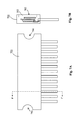
- FIG. 2A is a top view and FIG. 2B is a cross-sectional view perpendicular to AA plane of a lead frame strip in examples of the present disclosure.
- FIGS. 3A, 4A, 5A, 6A, 7A and 7C are a series of top views and FIGS. 3B, 4B, 5B, 6B, 7B and 7D are a series of cross-sectional views perpendicular to BB, CC, DD, EE, FF and GG planes respectively showing various processing steps to fabricate semiconductor power devices in examples of the present disclosure.
- FIG. 8A is a top view and FIG. 8B is a cross-sectional view perpendicular to HH plane of a semiconductor power device in examples of the present disclosure.
- FIG. 8C is a top view and FIG. 8D is a cross-sectional view perpendicular to II plane of a semiconductor power device in examples of the present disclosure.
- FIG. 9 is a top view of a semiconductor power device in examples of the present disclosure.
- FIG. 10 is a top view of a semiconductor power device in examples of the present disclosure.
- FIG. 1 is a flowchart of a process 100 to fabricate semiconductor power devices in examples of the present disclosure.
- the process 100 may begin in block 102 .
- a lead frame strip 200 of FIG. 2A having a plurality of lead frame units 202 and 204 of FIG. 2A (two lead frame units are shown) is provided.
- Two or more pluralities of single in-line leads 360 A, 360 B and 360 C of FIG. 3A are near a side of a lead frame unit 302 of FIG. 3A .
- the plurality of single in-line leads 360 A includes a source lead 362 (a first lead).
- the plurality of single in-line leads 360 B includes a source lead 364 .
- the plurality of single in-line leads 360 C includes a source lead 366 .
- the lead frame unit 302 is similar to the lead frame unit 202 of FIG. 2A . Portions of the lead frame unit 302 that will be removed during the singulation step in block 116 are not shown in FIG. 3A .
- Block 102 may be followed by block 104 .
- two or more high-side semiconductor chips 312 , 314 and 316 of FIG. 3A are attached to the lead frame unit 302 through a first layer of conductive bonding material.
- the conductive bonding material is solder paste, epoxy or a silver sintering material.
- Source pads 322 , 324 and 326 of FIG. 3A and gate pads 332 , 334 and 336 of FIG. 3A are on top surfaces of the high-side semiconductor chips 312 , 314 and 316 respectively. Drain pads are at bottom surfaces of the high-side semiconductor chips 312 , 314 and 316 respectively.
- Block 104 may be followed by block 106 .
- each of the high-side semiconductor chips 312 , 314 and 316 is connected to a source lead 362 , 364 or 366 (a first lead) of a respective plurality of single in-line leads of the two or more pluralities of single in-line leads 360 A, 360 B and 360 C by a respective clip of two or more first clips 442 , 444 and 446 .
- the clip 442 has a first end 452 , a bridge 456 and a second end 454 .
- the bridge 456 connects the first end 452 to the second end 454 .
- a bottom surface of the first end 452 is attached to a top surface of the high-side semiconductor chip 312 through a second layer of conductive bonding material.
- the source pad 322 of the high-side semiconductor chip 312 is electrically and mechanically connected to the clip 442 .
- a bottom surface of the second end 454 is attached to a top surface of the source lead 362 through a third layer of conductive bonding material.
- a region 472 of the top surface of the high-side semiconductor chip 312 is not covered by the clip 442 . Therefore, the gate pad 332 is accessible in the wire bonding step of block 112 .
- a region 474 of the top surface of the high-side semiconductor chip 314 is not covered by the clip 444 and a region 476 of the top surface of the high-side semiconductor chip 316 is not covered by the clip 446 .
- Block 106 may be followed by block 108 .
- a respective semiconductor chip of two or more low-side semiconductor chips 512 , 514 and 516 of FIG. 5A (three low-side semiconductor chips are shown) is attached to each clip of the two or more first clips 442 , 444 and 446 through a fourth layer of conductive bonding material.
- Source pads 522 , 524 and 526 of FIG. 5A and gate pads 532 , 534 and 536 of FIG. 5A are on top surfaces of the low-side semiconductor chips 512 , 514 and 516 respectively.
- Drain pads are at bottom surfaces of the low-side semiconductor chips 512 , 514 and 516 respectively.
- the drain of the low-side semiconductor chip 512 is electrically and mechanically connected to the source pad 322 of the high-side semiconductor chips 312 through the first end 452 of the clip 442 .
- Source leads 362 , 364 and 366 are also referred as phase note leads since the drains of the low-side semiconductor chips are also connected to the phase note leads through the first clips.
- each of the two or more pluralities of single in-line leads 360 A, 360 B and 360 C includes a phase note lead separated from each other.
- the phase note leads connected to each stack of high-side semiconductor chip and low-side semiconductor chip may connect together or share a common phase note lead (not shown).
- Block 108 may be followed by block 110 .
- a source pad 522 , 524 or 526 of each semiconductor chip of the two or more low-side semiconductor chips 512 , 514 and 516 is connected to ground.
- each of the source pad 522 , 524 or 526 of the low-side semiconductor chips 512 , 514 and 516 is connected to a ground lead 662 , 664 or 666 (a second lead) of a respective plurality of single in-line leads of the two or more pluralities of single in-line leads 360 A, 360 B and 360 C by a respective clip of two or more second clips 642 , 644 and 646 .
- the clip 642 has a first end 652 , a bridge 656 and a second end 654 .
- the bridge 656 connects the first end 652 to the second end 654 .
- a bottom surface of the first end 652 is attached to a top surface of the low-side semiconductor chip 512 through a fifth layer of conductive bonding material.
- the source pad 522 of the low-side semiconductor chip 512 is electrically and mechanically connected to the clip 642 .
- a bottom surface of the second end 654 is attached to a top surface of the ground lead 662 through a sixth layer of conductive bonding material.
- a linked clip 842 of FIG. 8A connects the source pad 522 , 524 or 526 on the top surface of the low-side semiconductor chips 512 , 514 and 516 to a ground lead 898 of FIG. 8A of the two or more pluralities of single in-line leads 360 A, 360 B and 360 C.
- the linked clip 842 has a first section 852 attached to the low-side semiconductor chip 512 , a second section 854 attached to the low-side semiconductor chip 514 , and a third section 856 attached to the low-side semiconductor chip 516 .
- a connecting member 862 connects the first section 852 to the second section 854 .
- a connecting member 864 connects the second section 854 to the third section 856 .
- a respective wire 982 , 984 or 986 of FIG. 9 connects the source pad 522 , 524 or 526 on the top surface of each of the two or more low-side semiconductor chips 512 , 514 and 516 to a ground lead 962 , 964 or 966 (a second lead) of the respective plurality of single in-line leads of the two or more pluralities of single in-line leads.
- wire 1062 of FIG. 10 connects the source pad 522 of the low-side semiconductor chip 512 to the source pad 524 of the low-side semiconductor chip 514 .
- Wire 1064 of FIG. 10 connects the source pad 524 of the low-side semiconductor chip 514 to the source pad 526 of the low-side semiconductor chip 516 .
- Wire 1096 of FIG. 10 connects the source pad 526 of the low-side semiconductor chip 516 to a ground lead 1098 .
- Block 110 may be followed by block 112 .
- a first respective wire 692 , 694 or 696 of FIG. 6A connects a gate pad 332 , 334 or 336 of said each of the two or more high-side semiconductor chips 312 , 314 and 316 to a third lead of the respective plurality of single in-line leads of the two or more pluralities of single in-line leads 360 A, 360 B and 360 C.
- a second respective wire 682 , 684 or 686 connects a gate pad 532 , 534 or 536 of said each of the two or more low-side semiconductor chips 512 , 514 and 516 to a fourth lead of the respective plurality of single in-line leads of the two or more pluralities of single in-line leads 360 A, 360 B and 360 C.
- Wires 682 , 684 , 686 , 692 , 694 and 696 may be replaced.
- wire bonding method may be replaced by clip attachments. Wire bonding method is preferred for cost reduction. Clip attachment is preferred when electrical current requirement is critical.
- Block 112 may be followed by block 114 .
- an encapsulation 722 of FIG. 7A is molded to cover a top surface of the lead frame strip 200 of FIG. 2A , the two or more high-side semiconductor chips 312 , 314 and 316 attached to each lead frame unit 302 of FIG. 3A , the respective clip of the two or more first clips 442 , 444 and 446 of FIG. 4A and the respective semiconductor chip of the two or more low-side semiconductor chips 512 , 514 and 516 .
- a majority portion of the respective clip of the two or more second clips 642 , 644 and 646 is embedded in the encapsulation 722 of FIGS. 7A and 7B .
- a clip is entirely embedded in the encapsulation 722 .
- a top surface 752 of FIG. 7D of the clip 742 of FIG. 7C and FIG. 7D is exposed from the encapsulation 722 .
- a bridge has a notch 762 of FIG. 7D . The bridge connects a first end of the clip 742 to a second end of the clip 742 .
- a lead frame unit is entirely embedded in the encapsulation 722 .
- a bottom surface 702 of FIG. 7D of the lead frame unit 302 is exposed from the encapsulation 722 .
- half circle cutouts 792 and 794 are formed for screw mounts.
- the linked clip 842 is entirely embedded in the encapsulation.
- top surfaces of the first section 852 , the second section 854 , and the third section 856 are exposed from the encapsulation 822 .
- a top surface 858 of the first section is exposed from the encapsulation 822 .
- Block 114 may be followed by block 116 .
- a semiconductor power device includes two or more semiconductor chip stacks.
- a first chip stack includes the lead frame unit 302 , the high-side semiconductor chip 312 , the clip 442 and the low-side semiconductor chip 512 .
- the first chip stack may further includes the clip 642 .
- the two or more first clips 442 , 444 and 446 , the two or more second clips 642 , 644 and 646 , and the linked clip 842 are made of a conductive metal material.
- the conductive metal material is copper.
- the conductive metal material is nickel.
Landscapes
- Engineering & Computer Science (AREA)
- Microelectronics & Electronic Packaging (AREA)
- Computer Hardware Design (AREA)
- Power Engineering (AREA)
- Physics & Mathematics (AREA)
- Condensed Matter Physics & Semiconductors (AREA)
- General Physics & Mathematics (AREA)
- Manufacturing & Machinery (AREA)
- Geometry (AREA)
- Lead Frames For Integrated Circuits (AREA)
- Wire Bonding (AREA)
- Ceramic Engineering (AREA)
Abstract
A semiconductor power device is disclosed. The semiconductor power device comprises a lead frame unit, two or more pluralities of single in-line leads, two or more semiconductor chip stacks, and a molding encapsulation. Each semiconductor chip stack includes a high-side semiconductor chip, a low-side semiconductor chip and a clip connecting a top surface of the high-side semiconductor chip to a bottom surface of the low-side semiconductor chip. This invention further discloses a method for fabricating semiconductor power devices. The method comprises the steps of providing a lead frame strip having a plurality of lead frame units; providing two or more pluralities of single in-line leads; attaching two or more high-side semiconductor chips to each lead frame unit; connecting each of the two or more high-side semiconductor chips to a respective lead by a respective clip of two or more first clips; attaching a respective low-side semiconductor chip of the two or more low-side semiconductor chips to each clip of the two or more first clips; molding an encapsulation; and singulating the lead frame strip and the encapsulation to form the semiconductor power devices.
Description
This invention relates generally to a semiconductor power device. More particularly, the present invention relates to a semiconductor power device having single in-line lead module and the method of making the semiconductor power device.
An electronic equipment, for example a power tool, may contain several power devices. Conventionally, metal-oxide semiconductor field-effect transistor (MOSFET) chips of those several power devices are fabricated and assembled in several different packages. The MOSFET chips are placed side-by-side. A pre-determined gap width between adjacent MOSFET chips is required to increase heat dissipation. Each package requires a separate pick-and-place process. It is not space efficient nor time efficient in a board level mounting step. It generates excessive impedance from board level interconnection.
The present disclosure discloses a semiconductor power device having semiconductor chip stacks. Each chip stack contains a high-side MOSFET chip, a low-side MOSFET chip and a clip connecting a source pad of the high-side MOSFET chip to a drain pad of the low-side MOSFET chip. In one example, clip interconnection is applied to a main power path, for example a source path or a drain path of a MOSFET chip of an N-channel module. In another example, a top surface of a clip is exposed from an encapsulation and a bottom surface of a lead frame unit is exposed from the encapsulation. It reduces the number of the pick-and-place processes. It is more space efficient and time efficient in a board level mounting step.
This invention discloses a semiconductor power device comprising a lead frame unit, two or more pluralities of single in-line leads, two or more semiconductor chip stacks and a molding encapsulation. Each semiconductor chip stack includes a high-side semiconductor chip, a low-side semiconductor chip and a clip connecting a top surface of the high-side semiconductor chip to a bottom surface of the low-side semiconductor chip.
This invention further discloses a method for fabricating semiconductor power devices. The method comprises the steps of providing a lead frame strip having a plurality of lead frame units; providing two or more pluralities of single in-line leads; attaching two or more high-side semiconductor chips to each lead frame unit; connecting each of the two or more high-side semiconductor chips to a respective lead by a respective clip of two or more first clips; attaching a respective low-side semiconductor chip of the two or more low-side semiconductor chips to each clip of the two or more first clips; molding an encapsulation; and singulating the lead frame strip and the encapsulation to form the semiconductor power devices.
In block 102, a lead frame strip 200 of FIG. 2A having a plurality of lead frame units 202 and 204 of FIG. 2A (two lead frame units are shown) is provided.
Two or more pluralities of single in-line leads 360A, 360B and 360C of FIG. 3A (three pluralities of single in-line leads are shown) are near a side of a lead frame unit 302 of FIG. 3A . The plurality of single in-line leads 360A includes a source lead 362 (a first lead). The plurality of single in-line leads 360B includes a source lead 364. The plurality of single in-line leads 360C includes a source lead 366. The lead frame unit 302 is similar to the lead frame unit 202 of FIG. 2A . Portions of the lead frame unit 302 that will be removed during the singulation step in block 116 are not shown in FIG. 3A . Block 102 may be followed by block 104.
In block 104, two or more high- side semiconductor chips 312, 314 and 316 of FIG. 3A (three high-side semiconductor chips are shown) are attached to the lead frame unit 302 through a first layer of conductive bonding material. In examples of the present disclosure, the conductive bonding material is solder paste, epoxy or a silver sintering material. Source pads 322, 324 and 326 of FIG. 3A and gate pads 332, 334 and 336 of FIG. 3A are on top surfaces of the high- side semiconductor chips 312, 314 and 316 respectively. Drain pads are at bottom surfaces of the high- side semiconductor chips 312, 314 and 316 respectively. Block 104 may be followed by block 106.
In block 106, each of the high- side semiconductor chips 312, 314 and 316 is connected to a source lead 362, 364 or 366 (a first lead) of a respective plurality of single in-line leads of the two or more pluralities of single in-line leads 360A, 360B and 360C by a respective clip of two or more first clips 442, 444 and 446. The clip 442 has a first end 452, a bridge 456 and a second end 454. The bridge 456 connects the first end 452 to the second end 454. A bottom surface of the first end 452 is attached to a top surface of the high-side semiconductor chip 312 through a second layer of conductive bonding material. In examples of the present disclosure, the source pad 322 of the high-side semiconductor chip 312 is electrically and mechanically connected to the clip 442. A bottom surface of the second end 454 is attached to a top surface of the source lead 362 through a third layer of conductive bonding material. A region 472 of the top surface of the high-side semiconductor chip 312 is not covered by the clip 442. Therefore, the gate pad 332 is accessible in the wire bonding step of block 112. Similarly, a region 474 of the top surface of the high-side semiconductor chip 314 is not covered by the clip 444 and a region 476 of the top surface of the high-side semiconductor chip 316 is not covered by the clip 446. Block 106 may be followed by block 108.
In block 108, a respective semiconductor chip of two or more low- side semiconductor chips 512, 514 and 516 of FIG. 5A (three low-side semiconductor chips are shown) is attached to each clip of the two or more first clips 442, 444 and 446 through a fourth layer of conductive bonding material. Source pads 522, 524 and 526 of FIG. 5A and gate pads 532, 534 and 536 of FIG. 5A are on top surfaces of the low- side semiconductor chips 512, 514 and 516 respectively. Drain pads are at bottom surfaces of the low- side semiconductor chips 512, 514 and 516 respectively. In examples of the present disclosure, the drain of the low-side semiconductor chip 512 is electrically and mechanically connected to the source pad 322 of the high-side semiconductor chips 312 through the first end 452 of the clip 442. Source leads 362, 364 and 366 are also referred as phase note leads since the drains of the low-side semiconductor chips are also connected to the phase note leads through the first clips. In the embodiment, each of the two or more pluralities of single in-line leads 360A, 360B and 360C includes a phase note lead separated from each other. Alternatively, the phase note leads connected to each stack of high-side semiconductor chip and low-side semiconductor chip may connect together or share a common phase note lead (not shown). Block 108 may be followed by block 110.
In block 110, a source pad 522, 524 or 526 of each semiconductor chip of the two or more low- side semiconductor chips 512, 514 and 516 is connected to ground. In examples of the present disclosure, each of the source pad 522, 524 or 526 of the low- side semiconductor chips 512, 514 and 516 is connected to a ground lead 662, 664 or 666 (a second lead) of a respective plurality of single in-line leads of the two or more pluralities of single in-line leads 360A, 360B and 360C by a respective clip of two or more second clips 642, 644 and 646. The clip 642 has a first end 652, a bridge 656 and a second end 654. The bridge 656 connects the first end 652 to the second end 654. A bottom surface of the first end 652 is attached to a top surface of the low-side semiconductor chip 512 through a fifth layer of conductive bonding material. In examples of the present disclosure, the source pad 522 of the low-side semiconductor chip 512 is electrically and mechanically connected to the clip 642. A bottom surface of the second end 654 is attached to a top surface of the ground lead 662 through a sixth layer of conductive bonding material.
In examples of the present disclosure, a linked clip 842 of FIG. 8A connects the source pad 522, 524 or 526 on the top surface of the low- side semiconductor chips 512, 514 and 516 to a ground lead 898 of FIG. 8A of the two or more pluralities of single in-line leads 360A, 360B and 360C. The linked clip 842 has a first section 852 attached to the low-side semiconductor chip 512, a second section 854 attached to the low-side semiconductor chip 514, and a third section 856 attached to the low-side semiconductor chip 516. A connecting member 862 connects the first section 852 to the second section 854. A connecting member 864 connects the second section 854 to the third section 856.
In examples of the present disclosure, a respective wire 982, 984 or 986 of FIG. 9 connects the source pad 522, 524 or 526 on the top surface of each of the two or more low- side semiconductor chips 512, 514 and 516 to a ground lead 962, 964 or 966 (a second lead) of the respective plurality of single in-line leads of the two or more pluralities of single in-line leads.
In examples of the present disclosure, wire 1062 of FIG. 10 connects the source pad 522 of the low-side semiconductor chip 512 to the source pad 524 of the low-side semiconductor chip 514. Wire 1064 of FIG. 10 connects the source pad 524 of the low-side semiconductor chip 514 to the source pad 526 of the low-side semiconductor chip 516. Wire 1096 of FIG. 10 connects the source pad 526 of the low-side semiconductor chip 516 to a ground lead 1098. Block 110 may be followed by block 112.
In block 112, wire bonding is applied. A first respective wire 692, 694 or 696 of FIG. 6A connects a gate pad 332, 334 or 336 of said each of the two or more high- side semiconductor chips 312, 314 and 316 to a third lead of the respective plurality of single in-line leads of the two or more pluralities of single in-line leads 360A, 360B and 360C. A second respective wire 682, 684 or 686 connects a gate pad 532, 534 or 536 of said each of the two or more low- side semiconductor chips 512, 514 and 516 to a fourth lead of the respective plurality of single in-line leads of the two or more pluralities of single in-line leads 360A, 360B and 360C. Wires 682, 684, 686, 692, 694 and 696 may be replaced. In one example, wire bonding method may be replaced by clip attachments. Wire bonding method is preferred for cost reduction. Clip attachment is preferred when electrical current requirement is critical. Block 112 may be followed by block 114.
In block 114, an encapsulation 722 of FIG. 7A is molded to cover a top surface of the lead frame strip 200 of FIG. 2A , the two or more high- side semiconductor chips 312, 314 and 316 attached to each lead frame unit 302 of FIG. 3A , the respective clip of the two or more first clips 442, 444 and 446 of FIG. 4A and the respective semiconductor chip of the two or more low- side semiconductor chips 512, 514 and 516.
In examples of the present disclosure, at least a majority portion of the respective clip of the two or more second clips 642, 644 and 646 is embedded in the encapsulation 722 of FIGS. 7A and 7B . In one example, a clip is entirely embedded in the encapsulation 722. In another example, a top surface 752 of FIG. 7D of the clip 742 of FIG. 7C and FIG. 7D is exposed from the encapsulation 722. In examples of the present disclosure, a bridge has a notch 762 of FIG. 7D . The bridge connects a first end of the clip 742 to a second end of the clip 742. In one example, a lead frame unit is entirely embedded in the encapsulation 722. In another example, a bottom surface 702 of FIG. 7D of the lead frame unit 302 is exposed from the encapsulation 722. In examples of the present disclosure, half circle cutouts 792 and 794 are formed for screw mounts.
In one example, the linked clip 842 is entirely embedded in the encapsulation. In another example, as shown in FIG. 8C and FIG. 8D , top surfaces of the first section 852, the second section 854, and the third section 856 are exposed from the encapsulation 822. In FIG. 8D , a top surface 858 of the first section is exposed from the encapsulation 822. Block 114 may be followed by block 116.
In block 116, the lead frame strip 200 and the encapsulation 722 are singulated to form the semiconductor power devices. In examples of the present disclosure, a semiconductor power device includes two or more semiconductor chip stacks. In one example, a first chip stack includes the lead frame unit 302, the high-side semiconductor chip 312, the clip 442 and the low-side semiconductor chip 512. The first chip stack may further includes the clip 642. In examples of the present disclosure, the two or more first clips 442, 444 and 446, the two or more second clips 642, 644 and 646, and the linked clip 842 are made of a conductive metal material. In one example, the conductive metal material is copper. In another example, the conductive metal material is nickel.
Those of ordinary skill in the art may recognize that modifications of the embodiments disclosed herein are possible. For example, the elevations of a first and second ends of a clip may vary. Other modifications may occur to those of ordinary skill in this art, and all such modifications are deemed to fall within the purview of the present invention, as defined by the claims.
Claims (10)
1. A semiconductor power device comprising:
a lead frame unit having a top surface and a bottom surface opposite the top surface;
two or more pluralities of single in-line leads arranged in a row near a side of the lead frame unit;
two or more semiconductor chip stacks each including
a high-side semiconductor chip having a top surface and a bottom surface, the bottom surface of the high-side semiconductor chip being attached to the top surface of the lead frame unit through a first layer of conductive bonding material;
a first clip having a first end and a second end, a bottom surface of the first end of the first clip being attached to a source pad on the top surface of the high-side semiconductor chip through a second layer of conductive bonding material, and a bottom surface of the second end of the first clip being attached to a top surface of a first lead of a respective plurality of single in-line leads of the two or more pluralities of single in-line leads through a third layer of conductive bonding material; and
a low-side semiconductor chip having a top surface and a bottom surface, the bottom surface of the low-side semiconductor chip being attached to the top surface of the first end of the first clip through a fourth layer of conductive bonding material; and
a molding encapsulation;
wherein a source pad on the top surface of the low-side semiconductor chip of said each of the two or more semiconductor chip stacks is electrically and mechanically connected to ground; and
wherein the high-side and low-side semiconductor chips and the first clip of said each of the two or more semiconductor chip stacks and at least a majority portion of the lead frame unit are embedded in the molding encapsulation.
2. The semiconductor power device of claim 1 , wherein the two or more semiconductor chip stacks each further including
a second clip having a first end and a second end, a bottom surface of the first end of the second clip being attached to the source pad on the top surface of the low-side semiconductor chip through a fifth layer of conductive bonding material, and a bottom surface of the second end of the second clip being attached to a top surface of a second lead of the respective plurality of single in-line leads of the two or more pluralities of single in-line leads through a sixth layer of conductive bonding material;
wherein the second lead is a ground lead; and
wherein at least a majority portion of the second clip is embedded in the molding encapsulation.
3. The semiconductor power device of claim 2 , wherein a first wire connects a gate pad of the high-side semiconductor chip to a third lead of the respective plurality of single in-line leads of the two or more pluralities of single in-line leads; and
wherein a second wire connects a gate pad of the low-side semiconductor chip to a fourth lead of the respective plurality of single in-line leads of the two or more pluralities of single in-line leads.
4. The semiconductor power device of claim 2 , wherein the bottom surface of the lead frame unit is exposed from the molding encapsulation.
5. The semiconductor power device of claim 2 , wherein a top surface of the second clip is exposed from the molding encapsulation.
6. The semiconductor power device of claim 2 , wherein a bridge connects the first end of the second clip to the second end of the second clip; and
wherein the bridge has a notch.
7. The semiconductor power device of claim 1 further comprising a linked clip connecting the source pad on the top surface of the low-side semiconductor chip of each of the two or more semiconductor chip stacks to a ground lead of the two or more pluralities of single in-line leads.
8. The semiconductor power device of claim 7 , wherein a top surface of the linked clip is exposed from the molding encapsulation.
9. The semiconductor power device of claim 1 , wherein a respective wire connects the source pad on the top surface of the low-side semiconductor chip of each of the two or more semiconductor chip stacks to a ground lead of the respective plurality of single in-line leads of the two or more pluralities of single in-line leads.
10. A semiconductor power device comprising:
a lead frame unit having a top surface and a bottom surface opposite the top surface;
two or more pluralities of single in-line leads arranged in a row near a side of the lead frame unit;
two or more semiconductor chip stacks each including
a high-side semiconductor chip having a top surface and a bottom surface, the bottom surface of the high-side semiconductor chip being attached to the top surface of the lead frame unit through a first layer of conductive bonding material;
a first clip having a first end and a second end, a bottom surface of the first end of the first clip being attached to a source pad on the top surface of the high-side semiconductor chip through a second layer of conductive bonding material, and a bottom surface of the second end of the first clip being attached to a top surface of a phase note lead through a third layer of conductive bonding material; and
a low-side semiconductor chip having a top surface and a bottom surface, the bottom surface of the low-side semiconductor chip being attached to the top surface of the first end of the first clip through a fourth layer of conductive bonding material; and
a molding encapsulation;
wherein a source pad on the top surface of the low-side semiconductor chip of said each of the two or more semiconductor chip stacks is electrically and mechanically connected to ground; and
wherein the high-side and low-side semiconductor chips and the first clip of said each of the two or more semiconductor chip stacks and at least a majority portion of the lead frame unit are embedded in the molding encapsulation.
Priority Applications (4)
| Application Number | Priority Date | Filing Date | Title |
|---|---|---|---|
| US15/191,414 US9754864B1 (en) | 2016-06-23 | 2016-06-23 | Semiconductor power device having single in-line lead module and method of making the same |
| TW105130534A TWI596728B (en) | 2016-06-23 | 2016-09-22 | Semiconductor power device having single in-line lead module and method of making the same |
| CN201610839778.0A CN107546191B (en) | 2016-06-23 | 2016-09-22 | Semiconductor power device with single-row in-line lead module and preparation method thereof |
| US15/659,587 US9966328B2 (en) | 2016-06-23 | 2017-07-25 | Semiconductor power device having single in-line lead module and method of making the same |
Applications Claiming Priority (1)
| Application Number | Priority Date | Filing Date | Title |
|---|---|---|---|
| US15/191,414 US9754864B1 (en) | 2016-06-23 | 2016-06-23 | Semiconductor power device having single in-line lead module and method of making the same |
Related Child Applications (1)
| Application Number | Title | Priority Date | Filing Date |
|---|---|---|---|
| US15/659,587 Division US9966328B2 (en) | 2016-06-23 | 2017-07-25 | Semiconductor power device having single in-line lead module and method of making the same |
Publications (1)
| Publication Number | Publication Date |
|---|---|
| US9754864B1 true US9754864B1 (en) | 2017-09-05 |
Family
ID=59701486
Family Applications (2)
| Application Number | Title | Priority Date | Filing Date |
|---|---|---|---|
| US15/191,414 Active US9754864B1 (en) | 2016-06-23 | 2016-06-23 | Semiconductor power device having single in-line lead module and method of making the same |
| US15/659,587 Active US9966328B2 (en) | 2016-06-23 | 2017-07-25 | Semiconductor power device having single in-line lead module and method of making the same |
Family Applications After (1)
| Application Number | Title | Priority Date | Filing Date |
|---|---|---|---|
| US15/659,587 Active US9966328B2 (en) | 2016-06-23 | 2017-07-25 | Semiconductor power device having single in-line lead module and method of making the same |
Country Status (3)
| Country | Link |
|---|---|
| US (2) | US9754864B1 (en) |
| CN (1) | CN107546191B (en) |
| TW (1) | TWI596728B (en) |
Cited By (1)
| Publication number | Priority date | Publication date | Assignee | Title |
|---|---|---|---|---|
| US11069604B2 (en) | 2018-12-18 | 2021-07-20 | Alpha And Omega Semiconductor (Cayman) Ltd. Grand | Semiconductor package and method of making the same |
Families Citing this family (4)
| Publication number | Priority date | Publication date | Assignee | Title |
|---|---|---|---|---|
| CN108133917A (en) * | 2018-01-26 | 2018-06-08 | 上海道之科技有限公司 | A kind of automobile-used power module of epoxy-plastic packaging of chip double-side welding |
| US11621203B2 (en) * | 2018-09-20 | 2023-04-04 | Semiconductor Components Industries, Llc | SiC MOSFET semiconductor packages and related methods |
| CN110010577A (en) * | 2019-04-08 | 2019-07-12 | 深圳市鹏源电子有限公司 | Direct insertion power device, semiconductor subassembly, In-wheel motor driving device or bus drive and new-energy automobile |
| US20210082790A1 (en) * | 2019-09-18 | 2021-03-18 | Alpha And Omega Semiconductor (Cayman) Ltd. | Power semiconductor package having integrated inductor and method of making the same |
Citations (3)
| Publication number | Priority date | Publication date | Assignee | Title |
|---|---|---|---|---|
| US8754510B2 (en) * | 2010-12-10 | 2014-06-17 | Panasonic Corporation | Conduction path, semiconductor device using the same, and method of manufacturing conduction path, and semiconductor device |
| US9595503B2 (en) * | 2010-09-09 | 2017-03-14 | Vishay-Siliconix | Dual lead frame semiconductor package and method of manufacture |
| US9607940B2 (en) * | 2013-07-05 | 2017-03-28 | Renesas Electronics Corporation | Semiconductor device |
Family Cites Families (9)
| Publication number | Priority date | Publication date | Assignee | Title |
|---|---|---|---|---|
| JP3876088B2 (en) * | 1999-01-29 | 2007-01-31 | ローム株式会社 | Semiconductor chip and multi-chip type semiconductor device |
| JP4637380B2 (en) * | 2001-02-08 | 2011-02-23 | ルネサスエレクトロニクス株式会社 | Semiconductor device |
| CN100435324C (en) * | 2004-12-20 | 2008-11-19 | 半导体元件工业有限责任公司 | Semiconductor package structure having enhanced thermal dissipation characteristics |
| JP4842118B2 (en) * | 2006-01-24 | 2011-12-21 | ルネサスエレクトロニクス株式会社 | Manufacturing method of semiconductor device |
| US7808102B2 (en) * | 2006-07-28 | 2010-10-05 | Alpha & Omega Semiconductor, Ltd. | Multi-die DC-DC boost power converter with efficient packaging |
| CN201011655Y (en) * | 2007-01-10 | 2008-01-23 | 上海凯虹科技电子有限公司 | Large power semiconductor device frame |
| US8399997B2 (en) * | 2011-06-10 | 2013-03-19 | Shanghai Kalhong Electronic Company Limited | Power package including multiple semiconductor devices |
| CN103035631B (en) * | 2011-09-28 | 2015-07-29 | 万国半导体(开曼)股份有限公司 | Combine the semiconductor device and manufacture method thereof that encapsulate high-end and low side chip |
| US8952509B1 (en) * | 2013-09-19 | 2015-02-10 | Alpha & Omega Semiconductor, Inc. | Stacked multi-chip bottom source semiconductor device and preparation method thereof |
-
2016
- 2016-06-23 US US15/191,414 patent/US9754864B1/en active Active
- 2016-09-22 TW TW105130534A patent/TWI596728B/en active
- 2016-09-22 CN CN201610839778.0A patent/CN107546191B/en active Active
-
2017
- 2017-07-25 US US15/659,587 patent/US9966328B2/en active Active
Patent Citations (3)
| Publication number | Priority date | Publication date | Assignee | Title |
|---|---|---|---|---|
| US9595503B2 (en) * | 2010-09-09 | 2017-03-14 | Vishay-Siliconix | Dual lead frame semiconductor package and method of manufacture |
| US8754510B2 (en) * | 2010-12-10 | 2014-06-17 | Panasonic Corporation | Conduction path, semiconductor device using the same, and method of manufacturing conduction path, and semiconductor device |
| US9607940B2 (en) * | 2013-07-05 | 2017-03-28 | Renesas Electronics Corporation | Semiconductor device |
Cited By (1)
| Publication number | Priority date | Publication date | Assignee | Title |
|---|---|---|---|---|
| US11069604B2 (en) | 2018-12-18 | 2021-07-20 | Alpha And Omega Semiconductor (Cayman) Ltd. Grand | Semiconductor package and method of making the same |
Also Published As
| Publication number | Publication date |
|---|---|
| TWI596728B (en) | 2017-08-21 |
| US20170372987A1 (en) | 2017-12-28 |
| CN107546191B (en) | 2020-02-21 |
| TW201801273A (en) | 2018-01-01 |
| CN107546191A (en) | 2018-01-05 |
| US9966328B2 (en) | 2018-05-08 |
Similar Documents
| Publication | Publication Date | Title |
|---|---|---|
| US9966328B2 (en) | Semiconductor power device having single in-line lead module and method of making the same | |
| US10930582B2 (en) | Semiconductor device having terminals directly attachable to circuit board | |
| US9425132B2 (en) | Stacked synchronous buck converter having chip embedded in outside recess of leadframe | |
| US9412684B2 (en) | Top exposed semiconductor chip package | |
| US7663211B2 (en) | Dual side cooling integrated power device package and module with a clip attached to a leadframe in the package and the module and methods of manufacture | |
| US7777315B2 (en) | Dual side cooling integrated power device module and methods of manufacture | |
| US20130087900A1 (en) | Thermally Enhanced Low Parasitic Power Semiconductor Package | |
| US11088055B2 (en) | Package with dies mounted on opposing surfaces of a leadframe | |
| JP2013168475A (en) | Semiconductor device and manufacturing method of the same | |
| WO2016073622A1 (en) | Triple stack semiconductor package | |
| US20170186674A1 (en) | Semiconductor packages and methods for forming same | |
| US9754862B2 (en) | Compound semiconductor device including a multilevel carrier | |
| JP2017511976A (en) | Converter with partially thinned leadframe with stacked chip and interposer | |
| US20130256920A1 (en) | Semiconductor device | |
| CN112530919B (en) | Common source planar grid array package | |
| CN110634812A (en) | Semiconductor device package with clip interconnect and dual side cooling | |
| US11145578B2 (en) | Semiconductor package with top or bottom side cooling and method for manufacturing the semiconductor package | |
| US20230326836A1 (en) | Semiconductor device package and method for manufacturing the same |
Legal Events
| Date | Code | Title | Description |
|---|---|---|---|
| AS | Assignment |
Owner name: ALPHA AND OMEGA SEMICONDUCTOR INCORPORATED, CALIFO Free format text: ASSIGNMENT OF ASSIGNORS INTEREST;ASSIGNORS:XUE, YAN XUN;NIU, ZHIQIANG;REEL/FRAME:039220/0904 Effective date: 20160721 |
|
| STCF | Information on status: patent grant |
Free format text: PATENTED CASE |
|
| MAFP | Maintenance fee payment |
Free format text: PAYMENT OF MAINTENANCE FEE, 4TH YEAR, LARGE ENTITY (ORIGINAL EVENT CODE: M1551); ENTITY STATUS OF PATENT OWNER: LARGE ENTITY Year of fee payment: 4 |