EP1801752A2 - Bildverarbeitungsschaltung und Bildverarbeitungsverfahren - Google Patents
Bildverarbeitungsschaltung und Bildverarbeitungsverfahren Download PDFInfo
- Publication number
- EP1801752A2 EP1801752A2 EP06126717A EP06126717A EP1801752A2 EP 1801752 A2 EP1801752 A2 EP 1801752A2 EP 06126717 A EP06126717 A EP 06126717A EP 06126717 A EP06126717 A EP 06126717A EP 1801752 A2 EP1801752 A2 EP 1801752A2
- Authority
- EP
- European Patent Office
- Prior art keywords
- pixel
- sub
- defect
- color data
- pixels
- Prior art date
- Legal status (The legal status is an assumption and is not a legal conclusion. Google has not performed a legal analysis and makes no representation as to the accuracy of the status listed.)
- Granted
Links
Images


Classifications
-
- G—PHYSICS
- G06—COMPUTING OR CALCULATING; COUNTING
- G06T—IMAGE DATA PROCESSING OR GENERATION, IN GENERAL
- G06T5/00—Image enhancement or restoration
- G06T5/77—Retouching; Inpainting; Scratch removal
-
- H—ELECTRICITY
- H04—ELECTRIC COMMUNICATION TECHNIQUE
- H04N—PICTORIAL COMMUNICATION, e.g. TELEVISION
- H04N23/00—Cameras or camera modules comprising electronic image sensors; Control thereof
- H04N23/10—Cameras or camera modules comprising electronic image sensors; Control thereof for generating image signals from different wavelengths
- H04N23/13—Cameras or camera modules comprising electronic image sensors; Control thereof for generating image signals from different wavelengths with multiple sensors
-
- G—PHYSICS
- G06—COMPUTING OR CALCULATING; COUNTING
- G06T—IMAGE DATA PROCESSING OR GENERATION, IN GENERAL
- G06T5/00—Image enhancement or restoration
- G06T5/20—Image enhancement or restoration using local operators
-
- H—ELECTRICITY
- H04—ELECTRIC COMMUNICATION TECHNIQUE
- H04N—PICTORIAL COMMUNICATION, e.g. TELEVISION
- H04N1/00—Scanning, transmission or reproduction of documents or the like, e.g. facsimile transmission; Details thereof
- H04N1/40—Picture signal circuits
- H04N1/401—Compensating positionally unequal response of the pick-up or reproducing head
-
- H—ELECTRICITY
- H04—ELECTRIC COMMUNICATION TECHNIQUE
- H04N—PICTORIAL COMMUNICATION, e.g. TELEVISION
- H04N23/00—Cameras or camera modules comprising electronic image sensors; Control thereof
- H04N23/10—Cameras or camera modules comprising electronic image sensors; Control thereof for generating image signals from different wavelengths
- H04N23/12—Cameras or camera modules comprising electronic image sensors; Control thereof for generating image signals from different wavelengths with one sensor only
-
- H—ELECTRICITY
- H04—ELECTRIC COMMUNICATION TECHNIQUE
- H04N—PICTORIAL COMMUNICATION, e.g. TELEVISION
- H04N25/00—Circuitry of solid-state image sensors [SSIS]; Control thereof
- H04N25/60—Noise processing, e.g. detecting, correcting, reducing or removing noise
- H04N25/68—Noise processing, e.g. detecting, correcting, reducing or removing noise applied to defects
- H04N25/683—Noise processing, e.g. detecting, correcting, reducing or removing noise applied to defects by defect estimation performed on the scene signal, e.g. real time or on the fly detection
-
- G—PHYSICS
- G06—COMPUTING OR CALCULATING; COUNTING
- G06T—IMAGE DATA PROCESSING OR GENERATION, IN GENERAL
- G06T2207/00—Indexing scheme for image analysis or image enhancement
- G06T2207/10—Image acquisition modality
- G06T2207/10024—Color image
Definitions
- the present invention relates to an image processing circuit and an image processing method, and more particularly, to a circuit and method for correcting pixel defects included in color image data.
- Solid state imaging devices such as a CCD
- a solid state device includes a matrix of pixels that receive light.
- Each pixel i.e., sub-pixel
- the image data of the pixels configures color image data.
- the pixels of a solid-state imaging device may include structural defects due to factors resulting from the manufacturing process. Thus, the image data generated by a pixel having a defect must be corrected with the image data generated by pixels located in the proximity of that defective pixel.
- a first prior art example of a solid state imaging device that generates color image data includes a filtering portion and an imaging portion.
- the filtering portion is formed by arranging one red filter (R), two green filters (Gr and Gb), and one blue filter (B) in a Bayer array.
- the imaging portion includes a plurality of light receiving elements for receiving the light that passes through each filter. Each light receiving element functions as a sub-pixel.
- Each pixel forming the color image data includes four filters and four light receiving elements.
- the color image data for each pixel is configured by the data for four colors (R, Gr, Gb, and B).
- the light receiving elements included in a solid state imaging device may include structural defects resulting from the manufacturing process. For example, the data amount corresponding to the amount of received light, or the so-called photoelectric conversion efficiency, for a certain light receiving element may differ from that of the other light receiving elements. As a result, the data for some of the four colors in the image data for that light receiving element may differ from the actual color of the image subject.
- An image processing circuit compares the data value for each color in the image data generated by the solid state imaging device with a threshold value to check for defects in each light receiving element. When a defect is found, the image processing circuit corrects the color data generated by the defective light receiving element.
- a single pixel is formed by four light receiving elements laid out on the same plane. Accordingly, the incident light amount in each light receiving element is one fourth of that of a single pixel. Thus, each light receiving element can use only one fourth of the light irradiating a single pixel region. Further, each light receiving element receives the light that passes through the corresponding filter in the Bayer array. Therefore, the red color light and blue color light are received in alternate lines and the light for each color is received by every other pixel. This widens the intervals between the light receiving elements for each color. As a result, it is difficult to increase the resolution.
- each of the three light receiving elements converts the light of the wavelength corresponding to the location of that light receiving element into an electric signal.
- the light receiving area of each light receiving element is the same as the area of a single pixel. Accordingly, each light receiving element converts all of the light entering the pixel into electric signals.
- the usage rate of the incident light amount is high compared to the first prior art example, and the data amount increases.
- the light receiving elements for each color are arranged adjacent to one another. This enables the resolution to be increased.
- the light receiving element in a pixel may include a defect.
- the light receiving elements are laid out in the direction perpendicular to the light receiving plane.
- the above image processing circuit does not defect the defect when the data values for the other colors do not exceed the threshold value even if the defect for the single color is detected.
- the defective color data is not corrected.
- the color data Mould differ from the actual color of the image subject and result in a color difference.
- the present invention provides an image processing circuit and an image processing method for correcting the value of a pixel included in color data to reduce color differences.
- One embodiment of the present invention is an image processing circuit for processing color data generated by a solid state imaging device.
- the solid state imaging device includes a matrix of a plurality of pixels, with each pixel including a plurality of sub-pixels arranged in a plurality of superimposed layers, and each sub-pixel corresponding to different color data.
- the image processing circuit includes a plurality of defect determination circuits respectively arranged in correspondence with the plurality of sub-pixels.
- the sub-pixel corresponding to each defect determination circuit defines a first sub-pixel, and a sub-pixel arranged near the first sub-pixel in the same layer as the first sub-pixel defines a second sub-pixel.
- Each of the defect determination circuits determines whether or not the corresponding first sub-pixel includes a defect based on the color data of the first sub-pixel and the color data of the second sub-pixel and generates a determination signal.
- a plurality of correction circuits are connected to each of the plurality of defect determination circuits, with the correction circuits respectively corresponding to the plurality of sub-pixels.
- Each of the correction circuits generates a corrected value for the corresponding first sub-pixel based on the color data of the first sub-pixel and the color data of the second sub-pixel when at least one of the determination signals is indicative of a defect.
- a further embodiment of the present invention is an image processing circuit for processing color data generated by a solid state imaging device.
- the solid state imaging device includes a matrix of a plurality of pixels. Each pixel includes a plurality of sub-pixels arranged in a plurality of superimposed layers, and each sub-pixel corresponds to different color data.
- the image processing circuit includes a plurality of first defect determination circuits respectively arranged in correspondence with the plurality of sub-pixels.
- the sub-pixel corresponding to each first defect determination circuit defines a first sub-pixel, and a sub-pixel arranged near the first sub-pixel in the same layer as the first sub-pixel defines a second sub-pixel.
- Each of the first defect determination circuits determines whether or not the corresponding first sub-pixel includes a defect based on the color data of the first sub-pixel and the color data of the second sub-pixel and generates a first determination signal.
- a plurality of second defect determination circuits respectively is arranged in correspondence with the plurality of sub-pixels.
- Each of the second defect determination circuits is connected to one or more first defect determination circuits associated with one or more first sub-pixels differing from the corresponding first sub-pixel.
- each second defect determination circuit determines whether or not the corresponding first sub-pixel includes a defect based on the color data of the first sub-pixel and the color data of the second sub-pixel and generates a second determination signal.
- a plurality of correction circuits respectively arranged in correspondence with the plurality of sub-pixels. Each of the correction circuits is connected to the corresponding first and second defect determination circuits. Each of the correction circuits generates a corrected value for the corresponding first sub-pixel based on the color data of the first sub-pixel and the color data of the second sub-pixel when at least one of the first and second determination signals is indicative of a defect.
- the present invention is a method for processing color data generated by a solid state imaging device.
- the solid state imaging device includes a matrix of a plurality of pixels.
- Each pixel includes a plurality of sub-pixels arranged in a plurality of superimposed layers, and each sub-pixel corresponds to different color data.
- the method includes providing each of a plurality of defect determination circuits respectively corresponding to the plurality of sub-pixels with color data of the corresponding sub-pixel defining a first sub-pixel and color data of a sub-pixel defining a second sub-pixel that is arranged near the first sub-pixel in the same layer as the first-sub pixel, generating a determination signal by determining whether or not the first sub-pixel includes a defect based on the color data of the first sub-pixel and the color data of the second sub-pixel with the corresponding defect determination circuit, providing each of a plurality of correction circuits respectively corresponding to the plurality of sub-pixels with the determination signals generated by the defect determination circuits, and generating a corrected value for the first sub-pixel based on the color data of the first sub-pixel and the color data of the second sub-pixel with the corresponding correction circuit when at least one of the determination signals is indicative of a defect.
- a further embodiment of the present invention is a method for processing color data generated by a solid state imaging device.
- the solid state imaging device includes a matrix of a plurality of pixels. Each pixel includes a plurality of sub-pixels arranged in a plurality of superimposed layers, and each sub-pixel corresponds to different color data.
- the method includes providing each of a plurality of first defect determination circuits respectively corresponding to the plurality of sub-pixels with color data of the corresponding sub-pixel defining a first sub-pixel and color data of a sub-pixel defining a second sub-pixel that is arranged near the first sub-pixel in the same layer as the first-sub pixel, generating a first determination signal by determining whether or not the first sub-pixel includes a defect based on the color data of the first sub-pixel and the color data of the second sub-pixel with the corresponding first defect determination circuit, providing each of a plurality of second defect determination circuits respectively corresponding to the plurality of sub-pixels with one or more first determination signals of one or more first defect determination circuits associated with one or more first sub-pixels differing from the corresponding first sub-pixel, generating a second determination signal by determining whether or not the first sub-pixel includes a defect based on the color data of the first sub-pixel and the color data of the second sub-pixel with the corresponding second defect determination circuit when the
- an image processing circuit 10 determines whether a pixel (sub-pixel) includes a defect based on color data Rin, Gin, Bin for red (R), green (G), and blue (B). When determining that a sub-pixel for at least one color has a defect, the image processing circuit 10 performs a correction process on the sub pixels for each color.
- the color data Rin, Gin, and Bin for each color is generated by a solid state imaging device, such as a CMOS image sensor.
- a solid state imaging device such as a CMOS image sensor.
- each pixel of the solid state imaging device is formed by three layers of light receiving elements (sub-pixels), or pixel sensors PB, PG, and PR, that are embedded in a silicon substrate. Silicon absorbs light of different colors at different depths.
- each of the layers of the pixels sensors PB, PG, and PR retrieves the color having a wavelength corresponding to its depth to generate a signal representing a pixel value corresponding to the amount of incident light.
- the image processing circuit 10 shown in Fig. 1 performs a defect determination process and a correction process based on the pixel value of a pixel (sub-pixel) that is subject to processing and a pixel value of at least one proximal pixel (sub-pixel) located proximal to the processing subject pixel.
- eight peripheral pixels (sub-pixels) adjacent to the processing subject pixel are used as the proximal pixels.
- the red color data Rin includes the pixel value for a processing subject pixel R11 and the pixel values for eight peripheral pixels R00, R01, R02, R10, R12, R20, R21, and R22 (R00 to R22). That is, the color data Rin includes the pixel values for three rows and three columns of pixels.
- the image processing circuit 10 determines whether or not the processing subject pixel R11 includes a defect. When the pixel R11 includes a defect, the image processing circuit 10 corrects the pixel value of the pixel R11 by generating a corrected pixel value. In the same manner, the green color data Gin includes the pixel value for a processing subject pixel G11 and the pixel values for eight peripheral pixels G00, G01, G02, G10, G12, G20, G21, and G22 (G00 to G22). The image processing circuit 10 determines whether or not the processing subject pixel G11 includes a defect.
- the image processing circuit 10 corrects the pixel value of the pixel G11 by generating a corrected pixel value.
- the blue color data Bin includes the pixel value for a processing subject pixel B11 and the pixel values for eight peripheral pixels B00, B01, B02, B10, B12, B20, B21, and B22 (B00 to B22).
- the image processing circuit 10 determines whether or not the processing subject pixel B11 includes a defect. When the pixel B11 includes a defect, the image processing circuit 10 corrects the pixel value of the pixel B11 by generating a corrected pixel value.
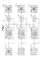
- the image processing circuit 10 includes three defect determination circuits 11R, 11G, and 11B and three correction circuits 12R, 12G, and 12B corresponding to the three colors, respectively.
- a threshold value T used to determine defects is set for each of the defect determination circuits 11R, 11G, and 11B.
- the defect determination circuit 11R for the red color determines whether or not the processing subject pixel R11 includes a defect. For example, in the first embodiment, the defect determination circuit 11R obtains a difference between the pixel value for the processing subject pixel R11 and an average value of the pixel values for a set of pixels lying along a line extending through the processing subject pixel R11. Then, the defect determination circuit 11R compares the absolute value of the difference (hereafter referred to as the difference value) with the threshold value T. The defect determination circuit 11R performs such a comparison process on each set of the peripheral pixels (four sets).
- the defect determination circuit 11R determines that the processing subject pixel R11 includes a defect when at least one of the difference values is greater than the threshold value T and determines that the processing subject pixel R11 is free from defects when each one of the difference values is less than or equal to the threshold value T.
- the defect determination circuit 11R compares the difference value of
- the defect determination circuit 11R when at least one difference value is greater than the threshold value T (i.e., when the processing subject pixel R11 includes a defect), the defect determination circuit 11R generates the determination signal SR at a high level. When each one of the difference values is less than or equal to the threshold value T, the defect determination circuit 11R generates the determination signal SR at a low level.
- the defect determination circuit 11G for the green color determines whether or not the processing subject pixel G11 includes a defect based on the green color data Gin and generates a determination signal SG indicative of the determination result. Further, the defect determination circuit 11B for the blue color determines whether or not the processing subject pixel B11 includes a defect based on the blue color data Bin and generates a determination signal SB indicative of the determination result.
- the determination signals SR, SG, and SB for the three colors are provided to each of the correction circuits 12R, 12G, and 12B. More specifically, each of the correction circuits 12R, 12G, and 12B is provided with a synthesized signal generating by obtaining the logical sum of the determination signals SR, SG, and SB, which are generated by the defect determination circuits 11R, 11G, and 11B.
- each of the correction circuits 12R, 12G, and 12B corrects the pixel value of the corresponding processing subject pixel R11, G11, and B11 based on the synthesized signal to generate a corrected pixel value.
- the red color correction circuit 12R uses the pixel value for the processing subject pixel R11 and the pixel values for the peripheral pixels to correct the pixel value of the pixel R11.
- the average value of the pixel values for the peripheral pixels is calculated and used as the corrected value for the processing subject pixel.
- the green correction circuit 12G corrects the pixel value of the processing subject pixel G11 based on the synthesized signal (determination signals SR, SG, and SB). Further, the blue correction circuit 12B corrects the pixel value of the processing subject pixel B11 based on the synthesized signal (determination signals SR, SG, and SB).
- the image processing circuit 10 corrects the pixel value of each one of the processing subject pixels R11, G11, and B11. This prevents color differences, which would be caused by defects.
- a pixel has the structure shown in Fig. 2, if the pixel sensor PR includes a defect, there is a high possibility that the other pixel sensors PG and PB in the same pixel also include defects.
- the prior art correction method for example, when the red pixel (pixel sensor) includes a defect, defects in the pixels (pixel sensor) of the other colors (G and B) may not be detected depending on the color of the image subject even though the G and B pixels include defects.
- the image processing circuit 10 of the present invention corrects the pixel values of each of the pixels R11, G11, and B11 when at least one of the processing subject pixels R11, G11, and B11 for the three colors includes a defect. This prevents color differences that would be caused by defects.
- the image processing circuit 10 of the first embodiment has the advantages described below.
- the defect determination circuit 11R for the red color determines whether or not the processing subject pixel R11 includes a defect and generates the determination signal SR.
- the defect determination circuits 11G and 11B for the green and blue colors generate the determination signals SG and SB respectively associated with the green and blue processing subject pixels G11 and B11.
- the correction circuits 12R, 12G, and 12B Based on the synthesized signal of the three determination signals SR, SG, and SB, the correction circuits 12R, 12G, and 12B generate the correction pixel values for the processing pixel values SR, SG, and SB using, for example, the pixel values of the corresponding peripheral pixels. Accordingly, when at least one of the processing subject pixels includes a defect, each of the correction circuits 12R, 12G, and 12B generates a corrected pixel value for the corresponding pixel. As a result, when any one of the processing subject pixels R11, G11, and B11 includes a defect, the processing subject pixels R11, G11, and B11 are all corrected. This reduces color differences.
- the image processing circuit 20 includes first defect determination circuits 11R, 11G, and 11B, second defect determination circuits 21R, 21G, and 21B, and correction circuits 12R, 12G, and 12B corresponding to red, green, and blue, respectively.
- First and second threshold values are set beforehand for the first and second defect determination circuits, respectively.
- the first defect determination circuits 11R, 11G, and 11B perform a first determination process to determine whether or not the processing subject pixels R11, G11, and B11 include a defect based on the corresponding color data Rin, Gin, and Bin. Then, the first defect determination circuits 11R, 11G, and 11B generate first determination signals SR, SG, and SB, respectively.
- the second defect determination circuits 21R, 21G, and 21B perform a second determination process based on the first determination signals and generate second determination signals SRa, SGa, and SBa.
- the second determination process is performed by using a second threshold value, which is equal to 1/n (n being a positive number that is greater than 1) of the first threshold value T used by the first defect determination circuits 11R, 11G, and 11B. More specifically, the second defect determination circuits 21R, 21G, and 21B compares the second threshold value T/n with a difference value, which is the same as that used by the first defect determination circuit.
- the second defect determination circuits 21R, 21G, and 21B determine whether or not the pixel sensors (processing subject pixels R11, G11, and B11) of the corresponding color include defects. Then, the second defect determination circuits 21R, 21G, and 21B generate second determination signals SRa, SGa, and SBa indicative of the determination results.
- the second defect determination circuit 21R for the red color determines whether or not the processing subject pixel R11 for the red color includes a defect based on the first determination signal SG of the first defect determination circuit 21G for the green color and the first determination signal SB of the first defect determination circuit 21B for the blue color. More specifically, the second defect determination circuit 21R calculates a difference value
- the second defect determination circuit 21R compares the difference value
- the second defect determination circuit 21R determines that the processing subject pixel R11 includes a defect and generates the second determination signal SRa at a high level.
- the second defect determination circuit 21R generates the second determination signal SRa at a low level.
- the second defect determination circuit 21R determines whether the processing subject pixel R11 includes a defect by using the second threshold value T/n, which is less then the first threshold value T of the first defect determination circuit 11R. Then, the second defect determination circuit 21R generates the second determination signal SRa that is indicative of the determination result.
- the second defect determination circuit 21G for the green color determines whether or not the processing subject pixel G11 for the green color includes a defect based on the first determination signals SR and SB of the first defect determination circuits 11R and 11B respectively corresponding to the red and blue colors.
- the second defect determination circuit 21B for the blue color determines whether or not the processing subject pixel B11 for the blue color includes a defect based on the first determination signals SR and SG of the first defect determination circuits 11R and 11G respectively corresponding to the red and green colors.
- the correction circuit 12R for the red color corrects the pixel value for the corresponding processing image pixel R11 to generate a corrected pixel value based on the signals SR and Sra.
- the correction circuit 12G for the green color corrects the pixel value for the corresponding processing image pixel G11 to generate a corrected pixel value based on the signals SG and SGa.
- the correction circuit 12B for the blue color corrects the pixel value for the corresponding processing image pixel B11 to generate a corrected pixel value based on the signals SB and SBa.
- the first defect determination circuit 11R for the color is generating the determination signal SR at a high level to indicate that the pixel R11 has a defect.
- the first defect determination circuits 11G and 11B for the green and blue colors are respectively generating the determination signals SG and SB at low levels indicating that the pixels G11 and B11 are free of defects.
- the first determination signals SG and SB for the green and blue colors indicate that there are no defects.
- the second defect determination circuit 21R for the red color does not perform the second determination process.
- the first determination signal SR for the red color indicates that there is a defect. Therefore, the second defect determination circuit 21G for the green color performs the second determination process.
- the second defect determination circuit 21G may determine that at least one of the difference values is greater than the second threshold value T/n. In such a case, the second defect determination circuit 21G generates the second determination signal SGa at a high level to indicate that the pixel G11 includes a defect. Further, since the first determination signal SR for the red color indicates that there is a defect, the second defect determination circuit 21B for the blue color performs the second determination process.
- the second defect determination circuit 21B may determine that the difference values are all less than the second threshold value T/n. In such a case, the second defect determination circuit 21B generates the second determination signal SBa at a low level to indicate that the pixel B11 is free from defects.
- the correction circuit 12R for the red color Based on first determination signal SR, which indicates that there is a defect, the correction circuit 12R for the red color performs the correction process to generate a corrected pixel value for the processing subject pixel R11. Based on the second determination signal SGa, which indicates that there is a defect, the correction circuit 12G for the green color performs the correction process to generate a corrected pixel value for the processing subject pixel G11. Based on the first determination signal SB and second determination signal SBa, each indicating that there is no defect, the correction circuit 12B for the blue color does not perform the correction process.
- the image processing circuit 20 of the second embodiment has the advantages described below.
- the first defect determination circuit 11R for the red color determines whether or not the processing subject pixel R11 includes a defect and generates the first determination signal SR.
- the first defect determination circuits 11G and lib for the green and blue colors generate the first determination signals SG and SB, respectively.
- the second defect determination circuit 21R determines whether or not the processing subject pixels G11 and B11 include defects.
- the second defect determination circuit 21R determines whether or not the processing subject pixel R11 includes a defect by using the difference values and the second threshold value T/n, which is less than the first threshold value, and generates the second determination signal SRa. In the same manner, the second defect determination circuits 21G and 21B for the green and blue colors generate the second determination signals SGa and SBa, respectively.
- the correction circuit 12R calculates a corrected pixel value for the pixel R11 from the pixel value of the pixel R11 and the pixel values of the peripheral pixels.
- the correction circuits 12G and 12B for the green and blue colors perform the same process as the correction circuit 12R.
- the second defect determination circuit 21R, 21G, or 21B may determine that the pixel includes a defect.
- the determination of whether or not a pixel includes a defect is accurately performed. This results in further optimal correction of the pixel values and further reduces color differences.
- the second defect determination circuits 21R, 21G, and 21B do not correct that corresponding pixel even if the other pixels are corrected.
- the pixels for each color are corrected independently. This avoids the generation of unnecessary corrected values. Accordingly, the pixel value of a processing subject pixel is prevented from differing from the actual color of the image subject.
- the threshold value (first threshold value) T of the first defect determination circuits 11R, 11G, and 11B and the second threshold value T/n of the second defect determination circuits 21R, 21G, and 21B may be varied for each color or each pixel.
- peripheral pixels located proximal to the processing subject pixel are not limited to the eight pixels arranged around the processing subject pixel.
- a versatile spatial filter may be used for the correction circuits 12R to 12B to calculate the corrected values. For example, each pixel value of the processing subject pixel R11 and the peripheral pixels R00 and R22 may be multiplied by a filter coefficient to use the total sum of the products as a corrected value. Alternatively, the total sum may be added to the original pixel value to obtain a corrected value. Further, a median filter may be used. This would facilitate the calculation of the corrected value based on the pixel value of the processing subject pixel and the pixel values of the proximal pixels (peripheral pixels).
Landscapes
- Engineering & Computer Science (AREA)
- Multimedia (AREA)
- Signal Processing (AREA)
- Physics & Mathematics (AREA)
- General Physics & Mathematics (AREA)
- Theoretical Computer Science (AREA)
- Color Television Image Signal Generators (AREA)
- Transforming Light Signals Into Electric Signals (AREA)
- Color Image Communication Systems (AREA)
Applications Claiming Priority (1)
| Application Number | Priority Date | Filing Date | Title |
|---|---|---|---|
| JP2005366970A JP4745816B2 (ja) | 2005-12-20 | 2005-12-20 | 画像処理回路及び画像処理方法 |
Publications (3)
| Publication Number | Publication Date |
|---|---|
| EP1801752A2 true EP1801752A2 (de) | 2007-06-27 |
| EP1801752A3 EP1801752A3 (de) | 2010-07-07 |
| EP1801752B1 EP1801752B1 (de) | 2018-05-02 |
Family
ID=37836636
Family Applications (1)
| Application Number | Title | Priority Date | Filing Date |
|---|---|---|---|
| EP06126717.5A Expired - Fee Related EP1801752B1 (de) | 2005-12-20 | 2006-12-20 | Bildverarbeitungsschaltung und Bildverarbeitungsverfahren |
Country Status (6)
| Country | Link |
|---|---|
| US (1) | US7978383B2 (de) |
| EP (1) | EP1801752B1 (de) |
| JP (1) | JP4745816B2 (de) |
| KR (1) | KR100893306B1 (de) |
| CN (1) | CN1988673B (de) |
| TW (1) | TWI369645B (de) |
Cited By (1)
| Publication number | Priority date | Publication date | Assignee | Title |
|---|---|---|---|---|
| US8164598B2 (en) | 2006-11-19 | 2012-04-24 | Barco N.V. | Display assemblies and computer programs and methods for defect compensation |
Families Citing this family (33)
| Publication number | Priority date | Publication date | Assignee | Title |
|---|---|---|---|---|
| JP2009302722A (ja) * | 2008-06-11 | 2009-12-24 | Nec Electronics Corp | 欠陥画素処理装置および欠陥画素処理方法 |
| US8835831B2 (en) | 2010-06-22 | 2014-09-16 | Zena Technologies, Inc. | Polarized light detecting device and fabrication methods of the same |
| US9299866B2 (en) | 2010-12-30 | 2016-03-29 | Zena Technologies, Inc. | Nanowire array based solar energy harvesting device |
| US8890271B2 (en) | 2010-06-30 | 2014-11-18 | Zena Technologies, Inc. | Silicon nitride light pipes for image sensors |
| US8299472B2 (en) | 2009-12-08 | 2012-10-30 | Young-June Yu | Active pixel sensor with nanowire structured photodetectors |
| US8269985B2 (en) | 2009-05-26 | 2012-09-18 | Zena Technologies, Inc. | Determination of optimal diameters for nanowires |
| US8866065B2 (en) | 2010-12-13 | 2014-10-21 | Zena Technologies, Inc. | Nanowire arrays comprising fluorescent nanowires |
| US8519379B2 (en) | 2009-12-08 | 2013-08-27 | Zena Technologies, Inc. | Nanowire structured photodiode with a surrounding epitaxially grown P or N layer |
| US8889455B2 (en) * | 2009-12-08 | 2014-11-18 | Zena Technologies, Inc. | Manufacturing nanowire photo-detector grown on a back-side illuminated image sensor |
| US8546742B2 (en) | 2009-06-04 | 2013-10-01 | Zena Technologies, Inc. | Array of nanowires in a single cavity with anti-reflective coating on substrate |
| US9000353B2 (en) | 2010-06-22 | 2015-04-07 | President And Fellows Of Harvard College | Light absorption and filtering properties of vertically oriented semiconductor nano wires |
| US9082673B2 (en) | 2009-10-05 | 2015-07-14 | Zena Technologies, Inc. | Passivated upstanding nanostructures and methods of making the same |
| US9515218B2 (en) | 2008-09-04 | 2016-12-06 | Zena Technologies, Inc. | Vertical pillar structured photovoltaic devices with mirrors and optical claddings |
| US9478685B2 (en) | 2014-06-23 | 2016-10-25 | Zena Technologies, Inc. | Vertical pillar structured infrared detector and fabrication method for the same |
| US8274039B2 (en) | 2008-11-13 | 2012-09-25 | Zena Technologies, Inc. | Vertical waveguides with various functionality on integrated circuits |
| US8748799B2 (en) | 2010-12-14 | 2014-06-10 | Zena Technologies, Inc. | Full color single pixel including doublet or quadruplet si nanowires for image sensors |
| US8791470B2 (en) | 2009-10-05 | 2014-07-29 | Zena Technologies, Inc. | Nano structured LEDs |
| US9406709B2 (en) | 2010-06-22 | 2016-08-02 | President And Fellows Of Harvard College | Methods for fabricating and using nanowires |
| US8735797B2 (en) | 2009-12-08 | 2014-05-27 | Zena Technologies, Inc. | Nanowire photo-detector grown on a back-side illuminated image sensor |
| US8229255B2 (en) * | 2008-09-04 | 2012-07-24 | Zena Technologies, Inc. | Optical waveguides in image sensors |
| US9343490B2 (en) | 2013-08-09 | 2016-05-17 | Zena Technologies, Inc. | Nanowire structured color filter arrays and fabrication method of the same |
| JP2010142464A (ja) * | 2008-12-19 | 2010-07-01 | Panasonic Corp | 画像処理装置および画像入力装置 |
| GB201011640D0 (en) * | 2010-07-12 | 2010-08-25 | Univ Sheffield | Radiation detection and method |
| JP5517883B2 (ja) * | 2010-10-20 | 2014-06-11 | キヤノン株式会社 | 画像処理装置及び画像処理方法 |
| GB201102478D0 (en) | 2011-02-11 | 2011-03-30 | Isdi Ltd | Radiation detector and method |
| KR20120114021A (ko) | 2011-04-06 | 2012-10-16 | 삼성디스플레이 주식회사 | 불량 픽셀 보정 방법 |
| JP5874317B2 (ja) * | 2011-10-27 | 2016-03-02 | 富士通株式会社 | イメージセンサ及び画像補正方法 |
| KR101896992B1 (ko) * | 2011-11-25 | 2018-09-11 | 엘지이노텍 주식회사 | 영상 처리 방법, 컴퓨터 판독 가능한 기록 매체 및 영상 처리 장치 |
| JP2013123812A (ja) * | 2011-12-13 | 2013-06-24 | Canon Inc | 検査装置、検査方法、コンピュータプログラム |
| US9113025B2 (en) | 2013-03-15 | 2015-08-18 | Samsung Electronics Co., Ltd. | Image signal processor circuits and methods for correcting crosstalk artifacts |
| GB2525625B (en) | 2014-04-29 | 2017-05-31 | Isdi Ltd | Device and method |
| CN105812756B (zh) * | 2016-03-16 | 2018-04-13 | 沈阳尚贤微创医疗器械股份有限公司 | 一种胶囊内窥镜无线传输数据丢失的修复补偿方法 |
| KR20240114118A (ko) * | 2023-01-16 | 2024-07-23 | 에스케이하이닉스 주식회사 | 이미지 처리 장치 및 이미지 처리 방법 |
Citations (1)
| Publication number | Priority date | Publication date | Assignee | Title |
|---|---|---|---|---|
| US20030193011A1 (en) | 2002-04-10 | 2003-10-16 | Canon Kabushiki Kaisha | Image pickup apparatus and image pickup method |
Family Cites Families (18)
| Publication number | Priority date | Publication date | Assignee | Title |
|---|---|---|---|---|
| JP2903956B2 (ja) * | 1993-07-06 | 1999-06-14 | 松下電器産業株式会社 | 画素欠陥補正装置 |
| JPH1062257A (ja) | 1996-08-20 | 1998-03-06 | Nippon Avionics Co Ltd | 赤外線2次元センサーカメラシステムの自動画素欠陥補正装置 |
| US6606120B1 (en) | 1998-04-24 | 2003-08-12 | Foveon, Inc. | Multiple storage node full color active pixel sensors |
| US6727691B2 (en) | 2000-06-26 | 2004-04-27 | Jentek Sensors, Inc. | High resolution inductive sensor arrays for material and defect characterization of welds |
| JP2003023570A (ja) * | 2001-07-06 | 2003-01-24 | Sanyo Electric Co Ltd | 画像データの修正方法及び画像信号処理装置 |
| JP3884952B2 (ja) | 2001-12-21 | 2007-02-21 | 株式会社日立製作所 | 撮像装置 |
| JP2004007425A (ja) | 2002-04-09 | 2004-01-08 | Canon Inc | 画像読取システム及び画像読取プログラム |
| JP3950726B2 (ja) * | 2002-04-09 | 2007-08-01 | キヤノン株式会社 | 固体撮像装置及び撮影システム |
| US7189951B2 (en) | 2002-04-09 | 2007-03-13 | Canon Kabushiki Kaisha | Solid-state image sensing apparatus and image sensing system |
| JP2003304544A (ja) * | 2002-04-10 | 2003-10-24 | Canon Inc | 撮像装置 |
| JP4297651B2 (ja) | 2002-07-01 | 2009-07-15 | 三洋電機株式会社 | 画像信号処理装置 |
| US7283164B2 (en) | 2002-09-18 | 2007-10-16 | Micron Technology, Inc. | Method for detecting and correcting defective pixels in a digital image sensor |
| US7301571B2 (en) * | 2003-01-17 | 2007-11-27 | Fujifilm Corporation | Method and imaging apparatus for correcting defective pixel of solid-state image sensor, and method for creating pixel information |
| KR100535636B1 (ko) | 2003-02-24 | 2005-12-08 | 매그나칩 반도체 유한회사 | 불량 화소 보상 기능을 갖는 이미지센서 |
| JP2004297267A (ja) | 2003-03-26 | 2004-10-21 | Sharp Corp | 画素欠陥処理装置 |
| CN1290059C (zh) * | 2003-04-18 | 2006-12-13 | 北京中星微电子有限公司 | 一种缺陷像素动态检测和补偿方法 |
| US7388609B2 (en) | 2003-07-07 | 2008-06-17 | Zoran Corporation | Dynamic identification and correction of defective pixels |
| KR100573487B1 (ko) | 2004-04-27 | 2006-04-24 | 매그나칩 반도체 유한회사 | 이미지센서 |
-
2005
- 2005-12-20 JP JP2005366970A patent/JP4745816B2/ja not_active Expired - Fee Related
-
2006
- 2006-12-20 CN CN2006101683044A patent/CN1988673B/zh not_active Expired - Fee Related
- 2006-12-20 KR KR1020060131006A patent/KR100893306B1/ko not_active Expired - Fee Related
- 2006-12-20 US US11/642,055 patent/US7978383B2/en not_active Expired - Fee Related
- 2006-12-20 EP EP06126717.5A patent/EP1801752B1/de not_active Expired - Fee Related
- 2006-12-20 TW TW095148080A patent/TWI369645B/zh not_active IP Right Cessation
Patent Citations (1)
| Publication number | Priority date | Publication date | Assignee | Title |
|---|---|---|---|---|
| US20030193011A1 (en) | 2002-04-10 | 2003-10-16 | Canon Kabushiki Kaisha | Image pickup apparatus and image pickup method |
Cited By (1)
| Publication number | Priority date | Publication date | Assignee | Title |
|---|---|---|---|---|
| US8164598B2 (en) | 2006-11-19 | 2012-04-24 | Barco N.V. | Display assemblies and computer programs and methods for defect compensation |
Also Published As
| Publication number | Publication date |
|---|---|
| KR100893306B1 (ko) | 2009-04-15 |
| JP4745816B2 (ja) | 2011-08-10 |
| EP1801752B1 (de) | 2018-05-02 |
| KR20070065840A (ko) | 2007-06-25 |
| TW200734966A (en) | 2007-09-16 |
| EP1801752A3 (de) | 2010-07-07 |
| JP2007174104A (ja) | 2007-07-05 |
| CN1988673A (zh) | 2007-06-27 |
| CN1988673B (zh) | 2010-05-19 |
| US20070139740A1 (en) | 2007-06-21 |
| US7978383B2 (en) | 2011-07-12 |
| TWI369645B (en) | 2012-08-01 |
Similar Documents
| Publication | Publication Date | Title |
|---|---|---|
| EP1801752B1 (de) | Bildverarbeitungsschaltung und Bildverarbeitungsverfahren | |
| US8817135B2 (en) | Correction of cluster defects in imagers | |
| CN101690242B (zh) | 固态图像传感装置 | |
| KR101012537B1 (ko) | 고체 이미지 센서 | |
| JP5589146B2 (ja) | 撮像素子及び撮像装置 | |
| JP5781998B2 (ja) | カラー撮像素子 | |
| JP2004112802A (ja) | 欠陥ピクセルの検出可能なディジタル・イメージ・センサおよび方法 | |
| JP2016048815A (ja) | 画像処理装置、画像処理方法、及び、画像処理システム | |
| CN102970463A (zh) | 图像处理设备、图像处理方法以及程序 | |
| JP2020092431A5 (de) | ||
| EP2742681A1 (de) | Bildverarbeitungsvorrichtung und steuerverfahren dafür | |
| KR20210156493A (ko) | 이미지 센싱 장치 | |
| US7304673B2 (en) | Image sensor array with substitutional circuit distribution | |
| JP5425343B2 (ja) | 撮像装置、撮像装置の制御方法、及び撮像装置の制御プログラム | |
| US9628730B2 (en) | Dark current gradient estimation using optically black pixels | |
| US11974054B2 (en) | Image sensor and camera having high sensitivity and high color reproducibility | |
| US7916790B2 (en) | Pixel compensation method for an image sensor | |
| JP2002223391A (ja) | 固体撮像素子の自動欠陥検出補正装置およびそれを用いた撮像装置 | |
| KR102346622B1 (ko) | 이미지 센서 및 이를 포함하는 촬상 장치 | |
| US11715749B2 (en) | Image sensing device and operating method thereof | |
| TWI528817B (zh) | 數位攝像裝置及其影像處理方法 | |
| JP2010025708A (ja) | 撮像素子の検査方法及び検査装置 | |
| JP2007017341A (ja) | 固体撮像素子の検査装置および検査方法 |
Legal Events
| Date | Code | Title | Description |
|---|---|---|---|
| PUAI | Public reference made under article 153(3) epc to a published international application that has entered the european phase |
Free format text: ORIGINAL CODE: 0009012 |
|
| AK | Designated contracting states |
Kind code of ref document: A2 Designated state(s): AT BE BG CH CY CZ DE DK EE ES FI FR GB GR HU IE IS IT LI LT LU LV MC NL PL PT RO SE SI SK TR |
|
| AX | Request for extension of the european patent |
Extension state: AL BA HR MK YU |
|
| RAP1 | Party data changed (applicant data changed or rights of an application transferred) |
Owner name: FUJITSU MICROELECTRONICS LIMITED |
|
| PUAL | Search report despatched |
Free format text: ORIGINAL CODE: 0009013 |
|
| RAP1 | Party data changed (applicant data changed or rights of an application transferred) |
Owner name: FUJITSU SEMICONDUCTOR LIMITED |
|
| AK | Designated contracting states |
Kind code of ref document: A3 Designated state(s): AT BE BG CH CY CZ DE DK EE ES FI FR GB GR HU IE IS IT LI LT LU LV MC NL PL PT RO SE SI SK TR |
|
| AX | Request for extension of the european patent |
Extension state: AL BA HR MK RS |
|
| 17P | Request for examination filed |
Effective date: 20110104 |
|
| AKX | Designation fees paid |
Designated state(s): DE |
|
| 17Q | First examination report despatched |
Effective date: 20110318 |
|
| RAP1 | Party data changed (applicant data changed or rights of an application transferred) |
Owner name: SOCIONEXT INC. |
|
| GRAP | Despatch of communication of intention to grant a patent |
Free format text: ORIGINAL CODE: EPIDOSNIGR1 |
|
| STAA | Information on the status of an ep patent application or granted ep patent |
Free format text: STATUS: GRANT OF PATENT IS INTENDED |
|
| INTG | Intention to grant announced |
Effective date: 20171121 |
|
| GRAS | Grant fee paid |
Free format text: ORIGINAL CODE: EPIDOSNIGR3 |
|
| GRAA | (expected) grant |
Free format text: ORIGINAL CODE: 0009210 |
|
| STAA | Information on the status of an ep patent application or granted ep patent |
Free format text: STATUS: THE PATENT HAS BEEN GRANTED |
|
| AK | Designated contracting states |
Kind code of ref document: B1 Designated state(s): DE |
|
| REG | Reference to a national code |
Ref country code: DE Ref legal event code: R096 Ref document number: 602006055288 Country of ref document: DE |
|
| REG | Reference to a national code |
Ref country code: DE Ref legal event code: R097 Ref document number: 602006055288 Country of ref document: DE |
|
| PLBE | No opposition filed within time limit |
Free format text: ORIGINAL CODE: 0009261 |
|
| STAA | Information on the status of an ep patent application or granted ep patent |
Free format text: STATUS: NO OPPOSITION FILED WITHIN TIME LIMIT |
|
| 26N | No opposition filed |
Effective date: 20190205 |
|
| PGFP | Annual fee paid to national office [announced via postgrant information from national office to epo] |
Ref country code: DE Payment date: 20191210 Year of fee payment: 14 |
|
| REG | Reference to a national code |
Ref country code: DE Ref legal event code: R082 Ref document number: 602006055288 Country of ref document: DE Representative=s name: HL KEMPNER PATENTANWALT, RECHTSANWALT, SOLICIT, DE |
|
| REG | Reference to a national code |
Ref country code: DE Ref legal event code: R119 Ref document number: 602006055288 Country of ref document: DE |
|
| PG25 | Lapsed in a contracting state [announced via postgrant information from national office to epo] |
Ref country code: DE Free format text: LAPSE BECAUSE OF NON-PAYMENT OF DUE FEES Effective date: 20210701 |