EP1779513B1 - Verstärkte passgatestrukturen zur leckstromverringerung - Google Patents
Verstärkte passgatestrukturen zur leckstromverringerung Download PDFInfo
- Publication number
- EP1779513B1 EP1779513B1 EP05778119A EP05778119A EP1779513B1 EP 1779513 B1 EP1779513 B1 EP 1779513B1 EP 05778119 A EP05778119 A EP 05778119A EP 05778119 A EP05778119 A EP 05778119A EP 1779513 B1 EP1779513 B1 EP 1779513B1
- Authority
- EP
- European Patent Office
- Prior art keywords
- passgate
- voltage
- integrated circuit
- transistors
- circuit defined
- Prior art date
- Legal status (The legal status is an assumption and is not a legal conclusion. Google has not performed a legal analysis and makes no representation as to the accuracy of the status listed.)
- Expired - Lifetime
Links
Images




Classifications
-
- H—ELECTRICITY
- H03—ELECTRONIC CIRCUITRY
- H03K—PULSE TECHNIQUE
- H03K19/00—Logic circuits, i.e. having at least two inputs acting on one output; Inverting circuits
- H03K19/02—Logic circuits, i.e. having at least two inputs acting on one output; Inverting circuits using specified components
- H03K19/173—Logic circuits, i.e. having at least two inputs acting on one output; Inverting circuits using specified components using elementary logic circuits as components
- H03K19/177—Logic circuits, i.e. having at least two inputs acting on one output; Inverting circuits using specified components using elementary logic circuits as components arranged in matrix form
- H03K19/1778—Structural details for adapting physical parameters
-
- H—ELECTRICITY
- H03—ELECTRONIC CIRCUITRY
- H03K—PULSE TECHNIQUE
- H03K19/00—Logic circuits, i.e. having at least two inputs acting on one output; Inverting circuits
- H03K19/02—Logic circuits, i.e. having at least two inputs acting on one output; Inverting circuits using specified components
- H03K19/173—Logic circuits, i.e. having at least two inputs acting on one output; Inverting circuits using specified components using elementary logic circuits as components
- H03K19/177—Logic circuits, i.e. having at least two inputs acting on one output; Inverting circuits using specified components using elementary logic circuits as components arranged in matrix form
- H03K19/1778—Structural details for adapting physical parameters
- H03K19/17784—Structural details for adapting physical parameters for supply voltage
-
- H—ELECTRICITY
- H03—ELECTRONIC CIRCUITRY
- H03K—PULSE TECHNIQUE
- H03K19/00—Logic circuits, i.e. having at least two inputs acting on one output; Inverting circuits
- H03K19/02—Logic circuits, i.e. having at least two inputs acting on one output; Inverting circuits using specified components
- H03K19/173—Logic circuits, i.e. having at least two inputs acting on one output; Inverting circuits using specified components using elementary logic circuits as components
- H03K19/177—Logic circuits, i.e. having at least two inputs acting on one output; Inverting circuits using specified components using elementary logic circuits as components arranged in matrix form
- H03K19/1778—Structural details for adapting physical parameters
- H03K19/17792—Structural details for adapting physical parameters for operating speed
Definitions
- NMOS passgate acts as an "open” or a "closed” switch.
- Document US 2003/05335 relates to structures and methods for selectively applying a well bias to only those portions of a PLD where such a bias is necessary or desirable, e.g., applying a positive well bias to transistors on critical paths within a user's design.
- a substrate for an integrated circuit includes a plurality of wells, each of which can be independently and programmably biased with the same or a different well bias voltage.
- FPGA implementation software automatically determines the critical paths and generates a configuration bitstream that enables positive well biasing only for the transistors participating in the critical paths, or only for programmable logic elements (e.g., CLBs or lookup tables) containing those transistors.
- negative well biasing is selectively applied to reduce leakage current.
- FIG. 3 is a simplified illustration of an aspect of another integrated circuit device which may be fabricated in accordance with the principles of the present invention.
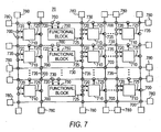
- FIG. 9 illustrates another aspect of the programmable logic device of FIG. 7 may be improved in accordance with the principles of the present invention.
- the passgate activation voltage may also be generated by any of a variety of voltage boosting/conversion circuitry such as charge pumps and voltage converters (e.g., DC/DC, AC/DC, etc.).
- the passgate activation voltage may be provided by a memory cell such as an SRAM-cell.
- FIG. 3 shows a portion of an integrated circuit device 30, which is divided into different sections 301/302/303, wherein all the transistors within a given section have been fabricated with a specific threshold voltage that may be different from that of the transistors in the other sections.
- sections 301 and 302 may each be a routing network with a high concentration of passgates (which may be used to construct, for example, interconnection switches and multiplexers). Accordingly, the transistors in sections 301 and 302 could be fabricated with a V T that is higher than that of the transistors in other sections 303.
- a triple-well process may be used to allow p-well 405 to be biased separately from the p-substrate 520, thereby allowing the V T of NMOS passgate 400 to be adjusted as a function of the source-to-bulk potential difference, V SB , which, in the arrangement shown in FIG. 5 , is dependent on V BIAS .
- FIG. 10 shows a portion of an integrated circuit 1000 employing the use of memory cells 1010 to drive passgate transistors 700/900 according to the principles of the present invention.
- Memory cells 1010 may be configurable ram cells such as SRAM cells.
- Passgate transistors 700/900 may be any of the enhanced passgate structures that have been described in the foregoing.
- Soft-error occurs when the logic state being stored in the memory cell inadvertently changes.
- Soft-error can be caused by, for example, sub-atomic particles (sometimes referred to as alpha particles or neutron beams) that disrupt the operation of silicon by changing the charge of the memory cell.
- Soft-error can also be caused by cross-coupling of memory cells.
- supply voltages e.g., nominal voltages
- Vccx as opposed to a nominal voltage, provides a supply voltage that enables memory cells 1010 to operate with a relatively low soft-error-rate.
Landscapes
- Physics & Mathematics (AREA)
- Mathematical Physics (AREA)
- Engineering & Computer Science (AREA)
- Computer Hardware Design (AREA)
- Computing Systems (AREA)
- General Engineering & Computer Science (AREA)
- Semiconductor Integrated Circuits (AREA)
- Design And Manufacture Of Integrated Circuits (AREA)
- Logic Circuits (AREA)
- Junction Field-Effect Transistors (AREA)
- Metal-Oxide And Bipolar Metal-Oxide Semiconductor Integrated Circuits (AREA)
- Static Random-Access Memory (AREA)
Claims (22)
- Integrierte Schaltung (1190) mit:einer ersten Gruppe von Transistoren (200), die eine nominelle Schwellenspannung haben, wobei jeder Transistor der ersten Gruppe dadurch selektiv aktiviert werden kann, dass eine Nennspannung an seinen Gate-Anschluss angelegt wird;einer Gruppe von Pass-Gate-Transistoren (201, 700, 900), die eine Pass-Gate-Schwellenspannung haben, die um einen festgelegten Prozentsatz höher als die nominelle Schwellenspannung der Transistoren der ersten Gruppe ist, wobei jeder Pass-Gate-Transistor (201, 700, 900) dadurch selektiv aktiviert werden kann, dass eine Pass-Gate-Aktivierungsspannung an den Gate-Anschluss jedes Pass-Gate-Transistors angelegt wird, die größer als die Nennspannung ist; undmindestens einer Speicherzelle (1010), die mit einer Speicherzellen-Versorgungsspannung gespeist wird, die gleich der Pass-Gate-Aktivierungsspannung oder größer als diese ist, wobei die mindestens eine Speicherzelle mit mindestens einem der Pass-Gate-Transistoren verbunden ist und so betreibbar ist, dass sie die Pass-Gate-Aktivierungsspannung selektiv für einen Gate-Anschluss mindestens eines Pass-Gate-Transistors (201, 700, 900) bereitstellt.
- Integrierte Schaltung nach Anspruch 1, dadurch gekennzeichnet, dass der festgelegte Prozentsatz von einem Prozent bis zweihundert Prozent reicht.
- Integrierte Schaltung nach Anspruch 1, dadurch gekennzeichnet, dass der festgelegte Prozentsatz zwischen fünf Prozent und vierzig Prozent liegt.
- Integrierte Schaltung nach Anspruch 1, dadurch gekennzeichnet, dass der festgelegte Prozentsatz zwischen zehn Prozent und fünfunddreißig Prozent liegt.
- Integrierte Schaltung nach Anspruch 1, dadurch gekennzeichnet, dass der festgelegte Prozentsatz zwischen fünfzehn Prozent und dreißig Prozent liegt.
- Integrierte Schaltung nach Anspruch 1, dadurch gekennzeichnet, dass die Nennspannung eine Versorgungsspannung ist, die für die integrierte Schaltung (1190) bereitgestellt wird.
- Integrierte Schaltung nach Anspruch 1, die weiterhin eine Pass-Gate-Aktivierungsspannungsquelle aufweist, die die Pass-Gate-Aktivierungsspannung bereitstellt.
- Integrierte Schaltung nach Anspruch 7, dadurch gekennzeichnet, dass die Pass-Gate-Aktivierungsspannungsquelle von einem Pegelumsetzer, einer Ladungspumpe, einem Referenzspannungsgenerator, einer Spannungsteilerschaltung oder einem Eingangs-/Ausgangsstift in der integrierten Schaltung bereitgestellt wird.
- Integrierte Schaltung nach Anspruch 1, dadurch gekennzeichnet, dass die Speicherzelle (1010) eine SRAM-Zelle ist.
- Integrierte Schaltung nach Anspruch 1, dadurch gekennzeichnet, dass die Pass-Gate-Transistoren (201, 700, 900) NMOS-Transistoren sind.
- Integrierte Schaltung nach Anspruch 1, die weiterhin Folgendes aufweist:eine Anordnung von Logikblöcken (710);eine Vielzahl von Verbindungsleitungen (730, 735) undeine Vielzahl von Schaltern (700) zum programmierbaren Routen von Logiksignalen zwischen den Logikblöcken über die Verbindungsleitungen, wobei jeder Schalter mindestens einen der Pass-Gate-Transistoren enthält.
- Digitales Verarbeitungssystem mit:einem Verarbeitungsschaltungssystem;einem Systemspeicher, der mit dem Verarbeitungsschaltungssystem verbunden ist; undeiner integrierten Schaltung nach Anspruch 1, die mit dem Verarbeitungsschaltungssystem und dem Systemspeicher verbunden ist.
- Gedruckte Leiterplatte, auf die die integrierte Schaltung nach Anspruch 1 montiert ist.
- Gedruckte Leiterplatte nach Anspruch 13, die weiterhin einen Plattenspeicher aufweist, der auf die gedruckte Leiterplatte montiert ist und mit der integrierten Schaltungsanordnung verbunden ist.
- Gedruckte Leiterplatte nach Anspruch 14, die weiterhin ein Verarbeitungsschaltungssystem aufweist, das auf die gedruckte Leiterplatte montiert ist und mit der integrierten Schaltungsanordnung verbunden ist.
- Integrierte Schaltung nach Anspruch 10, die weiterhin eine Vielzahl von Speicherzellen aufweist, die mit einer Speicherzellen-Versorgungsspannung gespeist werden, die gleich der Pass-Gate-Aktivierungsspannung oder größer als diese ist.
- Integrierte Schaltung nach Anspruch 16, dadurch gekennzeichnet, dass die Speicherzellen die Pass-Gate-Aktivierungsspannung selektiv für die Pass-Gate-Transistoren bereitstellen.
- Integrierte Schaltung nach Anspruch 16, dadurch gekennzeichnet, dass die Speicherzellen SRAM-Zellen sind.
- Integrierte Schaltung nach Anspruch 16, dadurch gekennzeichnet, dass die Speicherzellen-Versorgungsspannung von einem Pegelumsetzer, einer Ladungspumpe, einem Referenzspannungsgenerator, einer Spannungsteilerschaltung oder einem Eingangs-/Ausgangsstift in der programmierbaren Logikschaltung bereitgestellt wird.
- Integrierte Schaltung nach Anspruch 10, dadurch gekennzeichnet, dass mindestens einer der Pass-Gate-Transistoren so hergestellt ist, dass er eine Schwellenspannung hat, die höher als die Schwellenspannung der anderen Transistoren ist.
- Integrierte Schaltung nach Anspruch 10, dadurch gekennzeichnet, dass mindestens einer der Pass-Gate-Transistoren ein Halbleitertransistor ist, der einen Gate-Wannen-Bereich und eine Verbindung zum Vormagnetisieren des Gate-Wannen-Bereichs in Bezug auf andere Bereiche des Halbleitertransistors hat, wodurch eine Schwellenspannung des Pass-Gate-Transistors auf einen Spannungspegel eingestellt wird, der höher als die nominelle Schwellenspannung ist.
- Integrierte Schaltung nach Anspruch 10, dadurch gekennzeichnet, dass die Pass-Gate-Transistoren NMOS-Transistoren sind.
Applications Claiming Priority (2)
| Application Number | Priority Date | Filing Date | Title |
|---|---|---|---|
| US10/910,891 US7292065B2 (en) | 2004-08-03 | 2004-08-03 | Enhanced passgate structures for reducing leakage current |
| PCT/US2005/027416 WO2006017501A1 (en) | 2004-08-03 | 2005-08-02 | Enhanced passgate structures for reducing leakage current |
Publications (2)
| Publication Number | Publication Date |
|---|---|
| EP1779513A1 EP1779513A1 (de) | 2007-05-02 |
| EP1779513B1 true EP1779513B1 (de) | 2012-03-14 |
Family
ID=35756807
Family Applications (1)
| Application Number | Title | Priority Date | Filing Date |
|---|---|---|---|
| EP05778119A Expired - Lifetime EP1779513B1 (de) | 2004-08-03 | 2005-08-02 | Verstärkte passgatestrukturen zur leckstromverringerung |
Country Status (6)
| Country | Link |
|---|---|
| US (1) | US7292065B2 (de) |
| EP (1) | EP1779513B1 (de) |
| JP (1) | JP2008509604A (de) |
| CN (1) | CN101027838B (de) |
| AT (1) | ATE549797T1 (de) |
| WO (1) | WO2006017501A1 (de) |
Families Citing this family (12)
| Publication number | Priority date | Publication date | Assignee | Title |
|---|---|---|---|---|
| US5457410A (en) * | 1993-08-03 | 1995-10-10 | Btr, Inc. | Architecture and interconnect scheme for programmable logic circuits |
| JP4635188B2 (ja) * | 2006-07-25 | 2011-02-16 | 独立行政法人産業技術総合研究所 | 四端子二重絶縁ゲート電界トランジスタによるmos回路 |
| US7673202B2 (en) * | 2006-09-28 | 2010-03-02 | Cisco Technology, Inc. | Single event upset test circuit and methodology |
| US7893723B2 (en) * | 2007-12-29 | 2011-02-22 | Texas Instruments Incorporated | Minimizing leakage in logic designs |
| JP5414061B2 (ja) * | 2010-03-24 | 2014-02-12 | 独立行政法人産業技術総合研究所 | パストランジスタを用いた論理回路、セレクター回路及び集積回路 |
| US8581625B2 (en) * | 2011-05-19 | 2013-11-12 | Semiconductor Energy Laboratory Co., Ltd. | Programmable logic device |
| US8804407B1 (en) | 2011-07-12 | 2014-08-12 | Altera Corporation | PMOS pass gate |
| US8723592B2 (en) * | 2011-08-12 | 2014-05-13 | Nxp B.V. | Adjustable body bias circuit |
| US8705605B1 (en) | 2011-11-03 | 2014-04-22 | Altera Corporation | Technique for providing loopback testing with single stage equalizer |
| US8995175B1 (en) * | 2012-01-13 | 2015-03-31 | Altera Corporation | Memory circuit with PMOS access transistors |
| US9628081B2 (en) * | 2014-08-12 | 2017-04-18 | Xilinx, Inc. | Interconnect circuits having low threshold voltage P-channel transistors for a programmable integrated circuit |
| CN112951830B (zh) * | 2021-02-01 | 2023-02-07 | 泉芯集成电路制造(济南)有限公司 | 集成电路器件、存储器和电子设备 |
Family Cites Families (41)
| Publication number | Priority date | Publication date | Assignee | Title |
|---|---|---|---|---|
| USRE34363E (en) | 1984-03-12 | 1993-08-31 | Xilinx, Inc. | Configurable electrical circuit having configurable logic elements and configurable interconnects |
| US4713557A (en) | 1984-09-26 | 1987-12-15 | Xilinx, Inc. | Bidirectional buffer amplifier |
| US4821233A (en) | 1985-09-19 | 1989-04-11 | Xilinx, Incorporated | 5-transistor memory cell with known state on power-up |
| US4831596A (en) | 1987-05-01 | 1989-05-16 | Texas Instruments Incorporated | Pass gate with low transistor junction breakdown susceptibility |
| JPH07105160B2 (ja) | 1989-05-20 | 1995-11-13 | 東芝マイクロエレクトロニクス株式会社 | 半導体記憶装置 |
| EP0615668A4 (de) | 1991-10-30 | 1995-03-01 | Xilinx Inc | Spannungsregler für einen ladungspumpengenerator. |
| US5291079A (en) | 1992-07-23 | 1994-03-01 | Xilinx, Inc. | Configuration control unit for programming a field programmable gate array and reading array status |
| US5455582A (en) * | 1992-12-17 | 1995-10-03 | Ulsi Technology, Inc. | Digital to analog converter employing R-2R ladders with substituted shunt arms |
| JP3189464B2 (ja) * | 1993-02-19 | 2001-07-16 | 株式会社デンソー | 回転位置検出装置 |
| JP3494469B2 (ja) * | 1994-05-26 | 2004-02-09 | 株式会社ルネサステクノロジ | フィールドプログラマブルゲートアレイ |
| US5544097A (en) * | 1995-03-31 | 1996-08-06 | Sgs-Thomson Microelectronics, Inc. | SRAM memory cell with reduced internal cell voltage |
| DE19524658C1 (de) | 1995-07-06 | 1996-10-24 | Siemens Ag | Bootstrapschaltung |
| US5717340A (en) | 1996-01-17 | 1998-02-10 | Xilink, Inc. | Circuit for testing pumped voltage gates in a programmable gate array |
| US5959933A (en) * | 1996-01-25 | 1999-09-28 | Micron Technology, Inc. | System for improved memory cell access |
| US6005806A (en) | 1996-03-14 | 1999-12-21 | Altera Corporation | Nonvolatile configuration cells and cell arrays |
| JPH09293789A (ja) * | 1996-04-24 | 1997-11-11 | Mitsubishi Electric Corp | 半導体集積回路 |
| US5821771A (en) * | 1996-05-21 | 1998-10-13 | Altera Corporation | Method and apparatus for monitoring or forcing an internal node in a programmable device |
| US5760605A (en) * | 1996-09-30 | 1998-06-02 | Advanced Micro Devices, Inc. | Programmable high speed routing switch |
| US5706226A (en) | 1996-12-31 | 1998-01-06 | Sgs-Thomson Microelectronics, Inc. | Low voltage CMOS SRAM |
| US6097238A (en) | 1997-01-10 | 2000-08-01 | Xilinx, Inc. | Circuit with ramp-up control and overcoming a threshold voltage loss in an NMOS transistor |
| US5877612A (en) * | 1997-03-24 | 1999-03-02 | The United States Of America As Represented By The Secretary Of The Navy | Amplification of signals from high impedance sources |
| US5880620A (en) | 1997-04-22 | 1999-03-09 | Xilinx, Inc. | Pass gate circuit with body bias control |
| US6535034B1 (en) | 1997-07-30 | 2003-03-18 | Programmable Silicon Solutions | High performance integrated circuit devices adaptable to use lower supply voltages with smaller device geometries |
| US5841694A (en) | 1997-07-30 | 1998-11-24 | Programmable Silicon Solutions | High performance programmable interconnect |
| JP3114680B2 (ja) * | 1997-12-15 | 2000-12-04 | 日本電気株式会社 | アクティブフィルタ |
| US6583662B1 (en) * | 1999-06-23 | 2003-06-24 | Globespanvirata, Inc. | Circuit and method for implementing an integrated continuous-time smoothing filter |
| US6278290B1 (en) | 1999-08-13 | 2001-08-21 | Xilinx, Inc. | Method and circuit for operating programmable logic devices during power-up and stand-by modes |
| US6396325B2 (en) | 1999-12-03 | 2002-05-28 | Fairchild Semiconductor Corporation | High frequency MOSFET switch |
| US6504212B1 (en) * | 2000-02-03 | 2003-01-07 | International Business Machines Corporation | Method and apparatus for enhanced SOI passgate operations |
| US6563367B1 (en) * | 2000-08-16 | 2003-05-13 | Altera Corporation | Interconnection switch structures |
| US6661253B1 (en) * | 2000-08-16 | 2003-12-09 | Altera Corporation | Passgate structures for use in low-voltage applications |
| US6577514B2 (en) * | 2001-04-05 | 2003-06-10 | Saifun Semiconductors Ltd. | Charge pump with constant boosted output voltage |
| MXPA01007171A (es) * | 2001-07-13 | 2003-01-27 | Hector Mendoza Orozco | Seguro mejorado para rifle deportivo de municiones. |
| CN1399407A (zh) * | 2001-07-26 | 2003-02-26 | 中国科学院微电子中心 | 自举式-互补传输门电荷恢复低功耗电路结构 |
| US6621325B2 (en) | 2001-09-18 | 2003-09-16 | Xilinx, Inc. | Structures and methods for selectively applying a well bias to portions of a programmable device |
| EP1438662A2 (de) | 2001-10-11 | 2004-07-21 | Altera Corporation | Fehlererkennung an programmierbaren logischen betriebsmitteln |
| JP3522248B2 (ja) | 2001-10-15 | 2004-04-26 | ローム株式会社 | 半導体集積回路装置 |
| US6492876B1 (en) * | 2001-10-25 | 2002-12-10 | National Semiconductor Corporation | Low power analog equalizer with variable op-amp gain |
| US6930510B2 (en) | 2003-03-03 | 2005-08-16 | Xilinx, Inc. | FPGA architecture with mixed interconnect resources optimized for fast and low-power routing and methods of utilizing the same |
| US6876572B2 (en) | 2003-05-21 | 2005-04-05 | Altera Corporation | Programmable logic devices with stabilized configuration cells for reduced soft error rates |
| WO2005013490A1 (en) | 2003-08-05 | 2005-02-10 | Koninklijke Philips Electronics N.V. | Switch module for a field programmable logic circuit |
-
2004
- 2004-08-03 US US10/910,891 patent/US7292065B2/en not_active Expired - Fee Related
-
2005
- 2005-08-02 CN CN2005800263612A patent/CN101027838B/zh not_active Expired - Fee Related
- 2005-08-02 JP JP2007524911A patent/JP2008509604A/ja not_active Withdrawn
- 2005-08-02 EP EP05778119A patent/EP1779513B1/de not_active Expired - Lifetime
- 2005-08-02 AT AT05778119T patent/ATE549797T1/de active
- 2005-08-02 WO PCT/US2005/027416 patent/WO2006017501A1/en not_active Ceased
Also Published As
| Publication number | Publication date |
|---|---|
| CN101027838B (zh) | 2010-10-27 |
| US20060028240A1 (en) | 2006-02-09 |
| CN101027838A (zh) | 2007-08-29 |
| JP2008509604A (ja) | 2008-03-27 |
| ATE549797T1 (de) | 2012-03-15 |
| US7292065B2 (en) | 2007-11-06 |
| EP1779513A1 (de) | 2007-05-02 |
| WO2006017501A1 (en) | 2006-02-16 |
Similar Documents
| Publication | Publication Date | Title |
|---|---|---|
| US7800405B2 (en) | Passgate structures for use in low-voltage applications | |
| EP1304803B1 (de) | Programmierbare logische Vorrichtung mit Silizium-auf-Isolator Transistoren | |
| JP4149011B2 (ja) | 集積回路を組立てる方法、集積回路、および集積回路のための高電圧許容インタフェース回路 | |
| US6940307B1 (en) | Integrated circuits with reduced standby power consumption | |
| EP0305676A2 (de) | CMOS-Ausgangstreiberschaltung | |
| US6262599B1 (en) | Level shifting CMOS I/O buffer | |
| CN101174828B (zh) | 具有开关选通门电路电平变换器的可编程多电源区 | |
| KR20000071306A (ko) | 과전압/부족전압 허용차 전달 게이트 | |
| US20060273825A1 (en) | Level conversion circuit and semiconductor integrated circuit device employing the level conversion circuit | |
| KR20000070951A (ko) | 고전압 cmos 레벨 시프터 | |
| KR20030006958A (ko) | 반도체 집적회로, 그 반도체 집적회로의 설계방법 및 그반도체 집적회로 설계용 프로그램 | |
| US7292065B2 (en) | Enhanced passgate structures for reducing leakage current | |
| US12407350B2 (en) | Voltage level shifter with programmable high supply voltage and high supply voltage-dependent variable low supply voltage | |
| JPH08148986A (ja) | 出力バッファ回路 | |
| US6998668B2 (en) | Semiconductor integrated circuit device including a level shifter | |
| WO2005048454A2 (en) | Multiplexer circuits | |
| US6064223A (en) | Low leakage circuit configuration for MOSFET circuits | |
| US7639042B2 (en) | Methods of reducing power in programmable logic devices using low voltage swing for routing signals | |
| US6028444A (en) | Three-statable net driver for antifuse field programmable gate array | |
| US6414518B1 (en) | Circuitry for a low internal voltage integrated circuit | |
| GB2334391A (en) | CMOS standby current reduction | |
| WO2005013490A1 (en) | Switch module for a field programmable logic circuit |
Legal Events
| Date | Code | Title | Description |
|---|---|---|---|
| PUAI | Public reference made under article 153(3) epc to a published international application that has entered the european phase |
Free format text: ORIGINAL CODE: 0009012 |
|
| 17P | Request for examination filed |
Effective date: 20070208 |
|
| AK | Designated contracting states |
Kind code of ref document: A1 Designated state(s): AT BE BG CH CY CZ DE DK EE ES FI FR GB GR HU IE IS IT LI LT LU LV MC NL PL PT RO SE SI SK TR |
|
| RIN1 | Information on inventor provided before grant (corrected) |
Inventor name: HOANG, TIM TRI Inventor name: LUI, HENRY Y. Inventor name: KABANI, MALIK Inventor name: PATEL, RAKESH |
|
| DAX | Request for extension of the european patent (deleted) | ||
| 17Q | First examination report despatched |
Effective date: 20100202 |
|
| REG | Reference to a national code |
Ref country code: DE Ref legal event code: R079 Ref document number: 602005033174 Country of ref document: DE Free format text: PREVIOUS MAIN CLASS: H03K0019000000 Ipc: H03K0019177000 |
|
| GRAP | Despatch of communication of intention to grant a patent |
Free format text: ORIGINAL CODE: EPIDOSNIGR1 |
|
| RIC1 | Information provided on ipc code assigned before grant |
Ipc: H03K 19/177 20060101AFI20111006BHEP |
|
| GRAS | Grant fee paid |
Free format text: ORIGINAL CODE: EPIDOSNIGR3 |
|
| GRAA | (expected) grant |
Free format text: ORIGINAL CODE: 0009210 |
|
| AK | Designated contracting states |
Kind code of ref document: B1 Designated state(s): AT BE BG CH CY CZ DE DK EE ES FI FR GB GR HU IE IS IT LI LT LU LV MC NL PL PT RO SE SI SK TR |
|
| REG | Reference to a national code |
Ref country code: GB Ref legal event code: FG4D |
|
| REG | Reference to a national code |
Ref country code: CH Ref legal event code: EP Ref country code: AT Ref legal event code: REF Ref document number: 549797 Country of ref document: AT Kind code of ref document: T Effective date: 20120315 |
|
| REG | Reference to a national code |
Ref country code: IE Ref legal event code: FG4D |
|
| REG | Reference to a national code |
Ref country code: DE Ref legal event code: R096 Ref document number: 602005033174 Country of ref document: DE Effective date: 20120510 |
|
| REG | Reference to a national code |
Ref country code: NL Ref legal event code: T3 |
|
| PG25 | Lapsed in a contracting state [announced via postgrant information from national office to epo] |
Ref country code: LT Free format text: LAPSE BECAUSE OF FAILURE TO SUBMIT A TRANSLATION OF THE DESCRIPTION OR TO PAY THE FEE WITHIN THE PRESCRIBED TIME-LIMIT Effective date: 20120314 |
|
| LTIE | Lt: invalidation of european patent or patent extension |
Effective date: 20120314 |
|
| PG25 | Lapsed in a contracting state [announced via postgrant information from national office to epo] |
Ref country code: GR Free format text: LAPSE BECAUSE OF FAILURE TO SUBMIT A TRANSLATION OF THE DESCRIPTION OR TO PAY THE FEE WITHIN THE PRESCRIBED TIME-LIMIT Effective date: 20120615 Ref country code: LV Free format text: LAPSE BECAUSE OF FAILURE TO SUBMIT A TRANSLATION OF THE DESCRIPTION OR TO PAY THE FEE WITHIN THE PRESCRIBED TIME-LIMIT Effective date: 20120314 Ref country code: FI Free format text: LAPSE BECAUSE OF FAILURE TO SUBMIT A TRANSLATION OF THE DESCRIPTION OR TO PAY THE FEE WITHIN THE PRESCRIBED TIME-LIMIT Effective date: 20120314 |
|
| REG | Reference to a national code |
Ref country code: AT Ref legal event code: MK05 Ref document number: 549797 Country of ref document: AT Kind code of ref document: T Effective date: 20120314 |
|
| PG25 | Lapsed in a contracting state [announced via postgrant information from national office to epo] |
Ref country code: CY Free format text: LAPSE BECAUSE OF FAILURE TO SUBMIT A TRANSLATION OF THE DESCRIPTION OR TO PAY THE FEE WITHIN THE PRESCRIBED TIME-LIMIT Effective date: 20120314 |
|
| PG25 | Lapsed in a contracting state [announced via postgrant information from national office to epo] |
Ref country code: RO Free format text: LAPSE BECAUSE OF FAILURE TO SUBMIT A TRANSLATION OF THE DESCRIPTION OR TO PAY THE FEE WITHIN THE PRESCRIBED TIME-LIMIT Effective date: 20120314 Ref country code: IS Free format text: LAPSE BECAUSE OF FAILURE TO SUBMIT A TRANSLATION OF THE DESCRIPTION OR TO PAY THE FEE WITHIN THE PRESCRIBED TIME-LIMIT Effective date: 20120714 Ref country code: SI Free format text: LAPSE BECAUSE OF FAILURE TO SUBMIT A TRANSLATION OF THE DESCRIPTION OR TO PAY THE FEE WITHIN THE PRESCRIBED TIME-LIMIT Effective date: 20120314 Ref country code: BE Free format text: LAPSE BECAUSE OF FAILURE TO SUBMIT A TRANSLATION OF THE DESCRIPTION OR TO PAY THE FEE WITHIN THE PRESCRIBED TIME-LIMIT Effective date: 20120314 Ref country code: CZ Free format text: LAPSE BECAUSE OF FAILURE TO SUBMIT A TRANSLATION OF THE DESCRIPTION OR TO PAY THE FEE WITHIN THE PRESCRIBED TIME-LIMIT Effective date: 20120314 Ref country code: SE Free format text: LAPSE BECAUSE OF FAILURE TO SUBMIT A TRANSLATION OF THE DESCRIPTION OR TO PAY THE FEE WITHIN THE PRESCRIBED TIME-LIMIT Effective date: 20120314 Ref country code: EE Free format text: LAPSE BECAUSE OF FAILURE TO SUBMIT A TRANSLATION OF THE DESCRIPTION OR TO PAY THE FEE WITHIN THE PRESCRIBED TIME-LIMIT Effective date: 20120314 Ref country code: PL Free format text: LAPSE BECAUSE OF FAILURE TO SUBMIT A TRANSLATION OF THE DESCRIPTION OR TO PAY THE FEE WITHIN THE PRESCRIBED TIME-LIMIT Effective date: 20120314 |
|
| PG25 | Lapsed in a contracting state [announced via postgrant information from national office to epo] |
Ref country code: SK Free format text: LAPSE BECAUSE OF FAILURE TO SUBMIT A TRANSLATION OF THE DESCRIPTION OR TO PAY THE FEE WITHIN THE PRESCRIBED TIME-LIMIT Effective date: 20120314 Ref country code: PT Free format text: LAPSE BECAUSE OF FAILURE TO SUBMIT A TRANSLATION OF THE DESCRIPTION OR TO PAY THE FEE WITHIN THE PRESCRIBED TIME-LIMIT Effective date: 20120716 |
|
| PLBE | No opposition filed within time limit |
Free format text: ORIGINAL CODE: 0009261 |
|
| STAA | Information on the status of an ep patent application or granted ep patent |
Free format text: STATUS: NO OPPOSITION FILED WITHIN TIME LIMIT |
|
| PG25 | Lapsed in a contracting state [announced via postgrant information from national office to epo] |
Ref country code: AT Free format text: LAPSE BECAUSE OF FAILURE TO SUBMIT A TRANSLATION OF THE DESCRIPTION OR TO PAY THE FEE WITHIN THE PRESCRIBED TIME-LIMIT Effective date: 20120314 Ref country code: DK Free format text: LAPSE BECAUSE OF FAILURE TO SUBMIT A TRANSLATION OF THE DESCRIPTION OR TO PAY THE FEE WITHIN THE PRESCRIBED TIME-LIMIT Effective date: 20120314 |
|
| 26N | No opposition filed |
Effective date: 20121217 |
|
| PG25 | Lapsed in a contracting state [announced via postgrant information from national office to epo] |
Ref country code: IT Free format text: LAPSE BECAUSE OF FAILURE TO SUBMIT A TRANSLATION OF THE DESCRIPTION OR TO PAY THE FEE WITHIN THE PRESCRIBED TIME-LIMIT Effective date: 20120314 |
|
| REG | Reference to a national code |
Ref country code: CH Ref legal event code: PL |
|
| PG25 | Lapsed in a contracting state [announced via postgrant information from national office to epo] |
Ref country code: MC Free format text: LAPSE BECAUSE OF NON-PAYMENT OF DUE FEES Effective date: 20120831 |
|
| REG | Reference to a national code |
Ref country code: DE Ref legal event code: R097 Ref document number: 602005033174 Country of ref document: DE Effective date: 20121217 |
|
| GBPC | Gb: european patent ceased through non-payment of renewal fee |
Effective date: 20120802 |
|
| PG25 | Lapsed in a contracting state [announced via postgrant information from national office to epo] |
Ref country code: LI Free format text: LAPSE BECAUSE OF NON-PAYMENT OF DUE FEES Effective date: 20120831 Ref country code: ES Free format text: LAPSE BECAUSE OF FAILURE TO SUBMIT A TRANSLATION OF THE DESCRIPTION OR TO PAY THE FEE WITHIN THE PRESCRIBED TIME-LIMIT Effective date: 20120625 Ref country code: CH Free format text: LAPSE BECAUSE OF NON-PAYMENT OF DUE FEES Effective date: 20120831 |
|
| REG | Reference to a national code |
Ref country code: IE Ref legal event code: MM4A |
|
| PG25 | Lapsed in a contracting state [announced via postgrant information from national office to epo] |
Ref country code: IE Free format text: LAPSE BECAUSE OF NON-PAYMENT OF DUE FEES Effective date: 20120802 Ref country code: BG Free format text: LAPSE BECAUSE OF FAILURE TO SUBMIT A TRANSLATION OF THE DESCRIPTION OR TO PAY THE FEE WITHIN THE PRESCRIBED TIME-LIMIT Effective date: 20120614 Ref country code: GB Free format text: LAPSE BECAUSE OF NON-PAYMENT OF DUE FEES Effective date: 20120802 |
|
| PG25 | Lapsed in a contracting state [announced via postgrant information from national office to epo] |
Ref country code: TR Free format text: LAPSE BECAUSE OF FAILURE TO SUBMIT A TRANSLATION OF THE DESCRIPTION OR TO PAY THE FEE WITHIN THE PRESCRIBED TIME-LIMIT Effective date: 20120314 |
|
| PG25 | Lapsed in a contracting state [announced via postgrant information from national office to epo] |
Ref country code: LU Free format text: LAPSE BECAUSE OF NON-PAYMENT OF DUE FEES Effective date: 20120802 |
|
| PG25 | Lapsed in a contracting state [announced via postgrant information from national office to epo] |
Ref country code: HU Free format text: LAPSE BECAUSE OF FAILURE TO SUBMIT A TRANSLATION OF THE DESCRIPTION OR TO PAY THE FEE WITHIN THE PRESCRIBED TIME-LIMIT Effective date: 20050802 |
|
| REG | Reference to a national code |
Ref country code: FR Ref legal event code: PLFP Year of fee payment: 12 |
|
| PGFP | Annual fee paid to national office [announced via postgrant information from national office to epo] |
Ref country code: NL Payment date: 20160805 Year of fee payment: 12 |
|
| PGFP | Annual fee paid to national office [announced via postgrant information from national office to epo] |
Ref country code: FR Payment date: 20160719 Year of fee payment: 12 |
|
| REG | Reference to a national code |
Ref country code: NL Ref legal event code: MM Effective date: 20170901 |
|
| REG | Reference to a national code |
Ref country code: FR Ref legal event code: ST Effective date: 20180430 |
|
| PG25 | Lapsed in a contracting state [announced via postgrant information from national office to epo] |
Ref country code: NL Free format text: LAPSE BECAUSE OF NON-PAYMENT OF DUE FEES Effective date: 20170901 |
|
| PG25 | Lapsed in a contracting state [announced via postgrant information from national office to epo] |
Ref country code: FR Free format text: LAPSE BECAUSE OF NON-PAYMENT OF DUE FEES Effective date: 20170831 |
|
| PGFP | Annual fee paid to national office [announced via postgrant information from national office to epo] |
Ref country code: DE Payment date: 20180717 Year of fee payment: 14 |
|
| REG | Reference to a national code |
Ref country code: DE Ref legal event code: R119 Ref document number: 602005033174 Country of ref document: DE |
|
| PG25 | Lapsed in a contracting state [announced via postgrant information from national office to epo] |
Ref country code: DE Free format text: LAPSE BECAUSE OF NON-PAYMENT OF DUE FEES Effective date: 20200303 |