EP1776849B1 - Schnittstellenbautstein - Google Patents
Schnittstellenbautstein Download PDFInfo
- Publication number
- EP1776849B1 EP1776849B1 EP05758615.8A EP05758615A EP1776849B1 EP 1776849 B1 EP1776849 B1 EP 1776849B1 EP 05758615 A EP05758615 A EP 05758615A EP 1776849 B1 EP1776849 B1 EP 1776849B1
- Authority
- EP
- European Patent Office
- Prior art keywords
- module
- contacts
- interface module
- interface
- component
- Prior art date
- Legal status (The legal status is an assumption and is not a legal conclusion. Google has not performed a legal analysis and makes no representation as to the accuracy of the status listed.)
- Expired - Lifetime
Links
Images

Classifications
-
- H—ELECTRICITY
- H05—ELECTRIC TECHNIQUES NOT OTHERWISE PROVIDED FOR
- H05K—PRINTED CIRCUITS; CASINGS OR CONSTRUCTIONAL DETAILS OF ELECTRIC APPARATUS; MANUFACTURE OF ASSEMBLAGES OF ELECTRICAL COMPONENTS
- H05K1/00—Printed circuits
- H05K1/02—Details
- H05K1/14—Structural association of two or more printed circuits
-
- H—ELECTRICITY
- H10—SEMICONDUCTOR DEVICES; ELECTRIC SOLID-STATE DEVICES NOT OTHERWISE PROVIDED FOR
- H10W—GENERIC PACKAGES, INTERCONNECTIONS, CONNECTORS OR OTHER CONSTRUCTIONAL DETAILS OF DEVICES COVERED BY CLASS H10
- H10W70/00—Package substrates; Interposers; Redistribution layers [RDL]
- H10W70/60—Insulating or insulated package substrates; Interposers; Redistribution layers
- H10W70/62—Insulating or insulated package substrates; Interposers; Redistribution layers characterised by their interconnections
- H10W70/63—Vias, e.g. via plugs
- H10W70/635—Through-vias
-
- G—PHYSICS
- G06—COMPUTING OR CALCULATING; COUNTING
- G06F—ELECTRIC DIGITAL DATA PROCESSING
- G06F1/00—Details not covered by groups G06F3/00 - G06F13/00 and G06F21/00
-
- G—PHYSICS
- G06—COMPUTING OR CALCULATING; COUNTING
- G06F—ELECTRIC DIGITAL DATA PROCESSING
- G06F13/00—Interconnection of, or transfer of information or other signals between, memories, input/output devices or central processing units
-
- H—ELECTRICITY
- H05—ELECTRIC TECHNIQUES NOT OTHERWISE PROVIDED FOR
- H05K—PRINTED CIRCUITS; CASINGS OR CONSTRUCTIONAL DETAILS OF ELECTRIC APPARATUS; MANUFACTURE OF ASSEMBLAGES OF ELECTRICAL COMPONENTS
- H05K1/00—Printed circuits
- H05K1/02—Details
- H05K1/14—Structural association of two or more printed circuits
- H05K1/144—Stacked arrangements of planar printed circuit boards
-
- H—ELECTRICITY
- H05—ELECTRIC TECHNIQUES NOT OTHERWISE PROVIDED FOR
- H05K—PRINTED CIRCUITS; CASINGS OR CONSTRUCTIONAL DETAILS OF ELECTRIC APPARATUS; MANUFACTURE OF ASSEMBLAGES OF ELECTRICAL COMPONENTS
- H05K3/00—Apparatus or processes for manufacturing printed circuits
- H05K3/30—Assembling printed circuits with electric components, e.g. with resistors
-
- H—ELECTRICITY
- H05—ELECTRIC TECHNIQUES NOT OTHERWISE PROVIDED FOR
- H05K—PRINTED CIRCUITS; CASINGS OR CONSTRUCTIONAL DETAILS OF ELECTRIC APPARATUS; MANUFACTURE OF ASSEMBLAGES OF ELECTRICAL COMPONENTS
- H05K1/00—Printed circuits
- H05K1/02—Details
- H05K1/14—Structural association of two or more printed circuits
- H05K1/141—One or more single auxiliary printed circuits mounted on a main printed circuit, e.g. modules, adapters
-
- H—ELECTRICITY
- H05—ELECTRIC TECHNIQUES NOT OTHERWISE PROVIDED FOR
- H05K—PRINTED CIRCUITS; CASINGS OR CONSTRUCTIONAL DETAILS OF ELECTRIC APPARATUS; MANUFACTURE OF ASSEMBLAGES OF ELECTRICAL COMPONENTS
- H05K2201/00—Indexing scheme relating to printed circuits covered by H05K1/00
- H05K2201/04—Assemblies of printed circuits
- H05K2201/049—PCB for one component, e.g. for mounting onto mother PCB
-
- H—ELECTRICITY
- H05—ELECTRIC TECHNIQUES NOT OTHERWISE PROVIDED FOR
- H05K—PRINTED CIRCUITS; CASINGS OR CONSTRUCTIONAL DETAILS OF ELECTRIC APPARATUS; MANUFACTURE OF ASSEMBLAGES OF ELECTRICAL COMPONENTS
- H05K2201/00—Indexing scheme relating to printed circuits covered by H05K1/00
- H05K2201/10—Details of components or other objects attached to or integrated in a printed circuit board
- H05K2201/10227—Other objects, e.g. metallic pieces
- H05K2201/10325—Sockets, i.e. female type connectors comprising metallic connector elements integrated in, or bonded to a common dielectric support
-
- H—ELECTRICITY
- H05—ELECTRIC TECHNIQUES NOT OTHERWISE PROVIDED FOR
- H05K—PRINTED CIRCUITS; CASINGS OR CONSTRUCTIONAL DETAILS OF ELECTRIC APPARATUS; MANUFACTURE OF ASSEMBLAGES OF ELECTRICAL COMPONENTS
- H05K2201/00—Indexing scheme relating to printed circuits covered by H05K1/00
- H05K2201/10—Details of components or other objects attached to or integrated in a printed circuit board
- H05K2201/10613—Details of electrical connections of non-printed components, e.g. special leads
- H05K2201/10621—Components characterised by their electrical contacts
- H05K2201/10734—Ball grid array [BGA]; Bump grid array
-
- H—ELECTRICITY
- H05—ELECTRIC TECHNIQUES NOT OTHERWISE PROVIDED FOR
- H05K—PRINTED CIRCUITS; CASINGS OR CONSTRUCTIONAL DETAILS OF ELECTRIC APPARATUS; MANUFACTURE OF ASSEMBLAGES OF ELECTRICAL COMPONENTS
- H05K2203/00—Indexing scheme relating to apparatus or processes for manufacturing printed circuits covered by H05K3/00
- H05K2203/17—Post-manufacturing processes
- H05K2203/176—Removing, replacing or disconnecting component; Easily removable component
-
- H—ELECTRICITY
- H05—ELECTRIC TECHNIQUES NOT OTHERWISE PROVIDED FOR
- H05K—PRINTED CIRCUITS; CASINGS OR CONSTRUCTIONAL DETAILS OF ELECTRIC APPARATUS; MANUFACTURE OF ASSEMBLAGES OF ELECTRICAL COMPONENTS
- H05K3/00—Apparatus or processes for manufacturing printed circuits
- H05K3/22—Secondary treatment of printed circuits
- H05K3/225—Correcting or repairing of printed circuits
-
- H—ELECTRICITY
- H05—ELECTRIC TECHNIQUES NOT OTHERWISE PROVIDED FOR
- H05K—PRINTED CIRCUITS; CASINGS OR CONSTRUCTIONAL DETAILS OF ELECTRIC APPARATUS; MANUFACTURE OF ASSEMBLAGES OF ELECTRICAL COMPONENTS
- H05K3/00—Apparatus or processes for manufacturing printed circuits
- H05K3/30—Assembling printed circuits with electric components, e.g. with resistors
- H05K3/32—Assembling printed circuits with electric components, e.g. with resistors electrically connecting electric components or wires to printed circuits
- H05K3/34—Assembling printed circuits with electric components, e.g. with resistors electrically connecting electric components or wires to printed circuits by soldering
- H05K3/341—Surface mounted components
- H05K3/3431—Leadless components
- H05K3/3436—Leadless components having an array of bottom contacts, e.g. pad grid array or ball grid array components
-
- H—ELECTRICITY
- H10—SEMICONDUCTOR DEVICES; ELECTRIC SOLID-STATE DEVICES NOT OTHERWISE PROVIDED FOR
- H10W—GENERIC PACKAGES, INTERCONNECTIONS, CONNECTORS OR OTHER CONSTRUCTIONAL DETAILS OF DEVICES COVERED BY CLASS H10
- H10W70/00—Package substrates; Interposers; Redistribution layers [RDL]
- H10W70/60—Insulating or insulated package substrates; Interposers; Redistribution layers
- H10W70/62—Insulating or insulated package substrates; Interposers; Redistribution layers characterised by their interconnections
- H10W70/65—Shapes or dispositions of interconnections
-
- H—ELECTRICITY
- H10—SEMICONDUCTOR DEVICES; ELECTRIC SOLID-STATE DEVICES NOT OTHERWISE PROVIDED FOR
- H10W—GENERIC PACKAGES, INTERCONNECTIONS, CONNECTORS OR OTHER CONSTRUCTIONAL DETAILS OF DEVICES COVERED BY CLASS H10
- H10W72/00—Interconnections or connectors in packages
- H10W72/071—Connecting or disconnecting
- H10W72/072—Connecting or disconnecting of bump connectors
- H10W72/07251—Connecting or disconnecting of bump connectors characterised by changes in properties of the bump connectors during connecting
-
- H—ELECTRICITY
- H10—SEMICONDUCTOR DEVICES; ELECTRIC SOLID-STATE DEVICES NOT OTHERWISE PROVIDED FOR
- H10W—GENERIC PACKAGES, INTERCONNECTIONS, CONNECTORS OR OTHER CONSTRUCTIONAL DETAILS OF DEVICES COVERED BY CLASS H10
- H10W72/00—Interconnections or connectors in packages
- H10W72/20—Bump connectors, e.g. solder bumps or copper pillars; Dummy bumps; Thermal bumps
Definitions
- the invention is based on an interface module with an integrated component according to the preamble of the independent claim.
- Such interface modules are used in various applications.
- One possibility is e.g. to replace a memory module of a control unit by such an interface module with integrated component.
- the actual memory module e.g. an EPROM, EEPROM, flash memory, RAM, etc. replaced by an interface module with a spare memory, e.g. by means of an emulator probe (ETK).
- EK emulator probe
- Such an interface module can also be referred to as a memory interface.
- This memory interface makes it possible to access a controller's memory data by means of a software tool via an external device, a tool computer (for example a PC) and to carry out measurement and application applications on the control device.
- JP 2002-141462 shows in the FIGS. 4 and FIG. 7 shows a multilayer packaging of a plurality of semiconductor elements.
- the prior art is the use of a printed circuit, which is installed between the control unit board and microcontroller.
- the microcontroller is removed from the production control unit and replaced by an intermediate socket.
- the microcontroller interface is plugged in, which contains the electronic components required for the protocol conversion, the access for the software tool or the tool computer (plug or cable) and a microcontroller in a standard housing. Due to this structure and the additional electronic components, the base area of the microcontroller interface, ie the interface module, is significantly larger than the area of the microcontroller itself.
- the entire interface module with integrated component is with its adaptation to the installation and its adaptation of the. Signals for transmission to the tool computer inseparably realized in a printed circuit.
- fitting to the location depends on the mechanical design (e.g., housing) and type of microcontroller, while matching the signals depends on the job being performed. For example, when measuring and adjusting, other microcontroller functions and interfaces must be accessed than during debugging. This gives a high number of interface module or interface variants that are expensive to manufacture and manage.
- the invention relates to an interface module with an integrated component, to replace a component on a circuit board, wherein the interface module at the bottom of the connection contacts are formed as provided for the contacts of the device on the board, the interface module advantageously in an adaptation part as the base module and a protocol converter part as a tool access module is divided, the base module is formed from an adapter socket and a carrier substrate, the carrier substrate on the bottom has the terminal contacts, and wherein via connections in the carrier substrate, the adapter contacts of the component arranged on the carrier substrate are connected to the connection contacts, and all the signals of the component required for the adaptation are guided on the upper side of the base module by the adaptation socket.
- the base module and the tool access module are connected via plug contacts and sockets, and the tool access module has electronic components for protocol conversion of local microcontroller buses into transferable protocols.
- this is the integrated component (1) integrated in the base module in chip-scale package technique whereby a smaller package is possible.
- the integrated component is contained in the base module and the base module contains an adaptation socket, wherein the integrated component and the adaptation socket are embodied as a ball-grid array (BGA).
- BGA ball-grid array
- the base module is formed from an adapter socket and a carrier substrate, wherein the adapter socket contains adapter contacts and the carrier substrate has the terminal contacts, wherein via connections, in particular lines, in the carrier substrate, the adapter contacts (are connected to the terminal contacts, whereby a very flexible Adaptation to various connection variants can be made.
- the tool access module is formed from a module substrate and an adapter, wherein the module substrate and the adapter are connected via adapter-substrate contacts.
- Another advantage is that the base module and the tool access module are connected via plug contacts and sockets, the adapter socket, the sockets and the adapter has the plug contacts.
- the integrated component is a microcontroller, which also includes processors, in particular special processors such as signal processors (DSP), etc., or other intelligent components.
- processors in particular special processors such as signal processors (DSP), etc., or other intelligent components.
- DSP signal processors
- the integrated component is a memory module, which in particular includes all programmable memory such as EPROM, PROM, RAM, EEPROM, flash memory, etc.
- the interface module or the microcontroller interface according to the invention thus has the advantage that the interface has almost the same or exactly the same base area as the component, e.g. has the microcontroller that replaces it. This significantly simplifies the coordination between tool manufacturer and ECU manufacturer.
- the ECU manufacturer is not subject to any board layout limitation. Any number of high-level components can be placed directly next to the microcontroller.
- adaptation part and protocol converter part greatly restricts the variety of variants, in particular of required microcontrollers.
- Interface modules with a standardized adaptation part or interface can reduce the number of products to be manufactured and simplify administration and maintenance. For every combination of microcontroller and executed activity, an ideal combination of adaptation part and protocol converter can thus be made available.
- the modules can be supplied by different providers. The modules are connected via emechanically reliable and automotive-suitable contacts.
- the drawing consists of different views of a highly simplified, not to scale exemplary embodiment of the interface module according to the invention inspesonder microcontroller interfaces or memory Inerfaces.
- the interface consists of two physically separate modules which can be plugged together by means of contacts: The basic module (marked with the numbers 1 to 8) implements the adaptation part, while the tool access module (marked with the letters A to E) realized the protocol part.
- Adaptation part and protocol converter are inseparably realized in a printed circuit.
- the adaptation part is dependent on the mechanical design (e.g., housing) and the type of microcontroller, while the protocol converter depends on the action being performed.
- This gives a high number of interface variants in the prior art, which are expensive to manufacture and manage.
- This is mastered and improved by the physical separation according to the invention into an adaptation part as basic module (100) and a protocol converter part as tool access module (200).
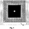
- the embodiment of the base module 100 of the interface module according to the invention is shown as a microcontroller interface or memory interface in the view from above.
- the adapter socket 3 forms the frame of the base module 100. It is a BGA socket (ball grid array) with double-row contacts on all four sides. For coding against rotation, a corner pin of the adaptation socket 3 is missing.
- the integrated component in particular the microcontroller or the Memory chip.
- the component in particular the microcontroller, is implemented as a chip-scale package (CSP).
- CSP chip-scale package
- the adaptation socket 3 and the microcontroller as integrated component 1 are designed as a ball-grid array (BGA) and soldered onto a carrier substrate 2. Alternatively, an adhesive method could also be used.
- BGA ball-grid array
- the described construction results in a base module 100 having the same footprint and the same pinout, ie the same terminal contact arrangement as the standard component, ie the standard microcontroller or standard memory which is normally used, in particular in the series, and according to the invention should be replaced.
- FIGS. 2 and 3 shows the embodiment of the interface module according to the invention or microcontroller interfaces from the side.
- FIG. 3 the base module and FIG. 2 the tool access module shows.
- FIG. 3 shows in the half left of the wavy line a cross-sectional view through the device, the microcontroller itself, so the inner of the base module and the half right of the wavy line shows the side view as a view from the outside of the base module 100th
- the adaptation socket 3 is also soldered (or otherwise connected) to the carrier substrate 2 via base contacts 5.
- the contacts of the base module 100 are mounted, which correspond to the pinout of the microcontroller in the standard housing.
- an interface module in particular in printed circuit board technology, shown with an IC device 1 in the chip-scale package and a surrounding adapter socket 3, the interface module from below the pinout 6 of the IC device in the standard housing and in the carrier substrate 2 all IC signals between chip scale package contacts or adapter contacts 8 and module connection contacts 6 are wired correctly and completely and all signals necessary for adaptation are guided to the uppermost layer of the carrier substrate 2 and connected to the contacts 5 of the adaptation socket 3 and at contact or socket sockets 4 at the top of the base module 100 are available.
- FIG. 2 the tool access module 200 is shown, which can be plugged onto the base module 100.
- This tool access module 200 consists of a module substrate D with electronic components E, which are connected at the bottom with an adapter B via adapter-substrate contacts C.
- Plug contacts A of the tool access module 200 establish the connection to the sockets 4 of the base module.
- a module substrate D in particular in printed circuit board technology, shown with one or more soldered or glued electronic components E, which is soldered or glued to a (BGA) adapter B, by means of plug contacts A on the contact or sockets. 4 of the basic module 100 can be connected.
- the electronic components E serve in particular for protocol conversion of local microcontroller buses into transferable protocols.
- a microcontroller bus come e.g. JTAG, Nexus or AUD or the local address, data and control bus.
- the said buses serve e.g. for connecting a calibration RAM, wherein the calibration RAM is designed in particular as a dual-ported RAM.
- the transferable protocol is in particular designed as a 100 Mbit / s Ethernet according to IEEE 802.3. It is also expedient to use a protocol according to IEEE 802.3u (100 Mbit / s) or IEEE 802.ab (1 Gbit / s).
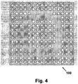
- FIG. 4 Finally, shows the same embodiment of the interface module according to the invention or microcontroller interfaces or memory interfaces from below.
- the carrier substrate 2 of the base module 100 has the same pinout, ie the same contacts 6 and almost the same or exactly the same area as the standard housing of the component, in particular of the microcontroller.
- the base module is connected via the terminal contacts 6 to the printed circuit board or board, in particular of the control unit.
Landscapes
- Engineering & Computer Science (AREA)
- Microelectronics & Electronic Packaging (AREA)
- Theoretical Computer Science (AREA)
- Physics & Mathematics (AREA)
- General Engineering & Computer Science (AREA)
- General Physics & Mathematics (AREA)
- Manufacturing & Machinery (AREA)
- Structures For Mounting Electric Components On Printed Circuit Boards (AREA)
- Details Of Connecting Devices For Male And Female Coupling (AREA)
- Coupling Device And Connection With Printed Circuit (AREA)
- Bus Control (AREA)
- Test And Diagnosis Of Digital Computers (AREA)
- Microcomputers (AREA)
Description
- Die Erfindung geht aus von einem Schnittstellenbaustein mit einem integrierten Bauelement gemäß dem Oberbegriff des unabhängigen Anspruchs.
- Solche Schnittstellenbausteine werden in verschiedenen Anwendungen eingesetzt. Eine Möglichkeit ist z.B. einen Speicherbaustein eines Steuergerätes durch einen solchen Schnittstellenbaustein mit integriertem Bauelement zu ersetzen. Dabei wird dann der eigentliche Speicherbaustein, z.B. ein EPROM, EEPROM, Flash-Speicher, RAM, usw. durch einen Schnittstellenbaustein mit einem Ersatzspeicher ersetzt, z.B. durch mittels eines Emulator Tastkopfes (ETK). Solch ein Schnittstellenbaustein kann auch als Speicher-Interface bezeichnet werden. Durch dieses Speicher-Interface ist es möglich auf Speicherdaten eines Steuergerätes mittels eines Software-Tools über ein externes Gerät einen Tool-Rechner (z.B. ein PC) zuzugreifen und Mess- und Apllikationsanwendungen an dem Steuergerät durchzuführen.
- Durch diesen Schnittstellenbaustein mit integriertem Bauelement können aber auch Microcontroller eines Steuergerätes selbst ersetzt werden, wobei es sich bei dem Bauelement dann eben um einen Microcontroller handelt. Im weiteren wird deshalb der Schnittstellenbaustein mit integriertem Bauelement als Microcontroller-Interface bezeichnet. Diese Bezeichnung ist aber nicht als Einschränkung bezüglich der Verwendung zu verstehen, wie die obigen Ausführungen belegen. Microcontroller-Interfaces sind nun insbesondere Vorrichtungen, die einem Software-Tool ermöglichen auf Signale von Microcontrollern (MCU) zuzugreifen. Der Microcontroller ist dabei am Einsatzort verbaut (z.B. in einem Steuergerät im Motorraum eines Kraftfahrzeuges)und sitzt dabei in der Regel auf einer Steuergeräteplatine oder Leiterplatte. Das Software-Tool wird auf einem externen Rechner, einem Tool-Rechner (beispielsweise einem PC) ausgeführt. Mit diesem Aufbau können verschiedene Tätigkeiten durchgeführt werden:
- Messen und Verstellen (Measurement & Calibration)
- Bypass-Anwendungen (Rapid-Prototyping)
- Fehlerbehebung sowie Funktions-und/oder Fehlerverfolgung
-
JP 2002-141462 Figuren 4 und 7 eine Multilayer-Verpackung von mehreren Halbleiterelementen. - Stand der Technik ist dabei die Verwendung einer gedruckten Schaltung, die zwischen Steuergeräte-Platine und Microcontroller eingebaut wird. Dazu wird der Microcontroller vom Seriensteuergerät entfernt und durch einen Zwischensockel ersetzt. Auf diesen Zwischensockel wird das Microcontroller-Interface aufgesteckt, welches die zur Protokoll-Wandlung benötigten elektronischen Bauteile, den Zugang für das Software-Tool bzw. den Tool-Rechner (Stecker oder Kabel) und einen Microcontroller in einem Standard-Gehäuse enthält. Durch diesen Aufbau und die zusätzlichen elektronischen Bauteile ist die Grundfläche des Microcontroller-Interfaces, also des Schnittstellenbausteins deutlich größer als die Fläche des Microcontrollers selbst.
- Dies stellt einen Nachteil da, da sich auf der Steuergeräte-Platine unter dem Schnittstellenbaustein also dem Microcontroller-Interface keine hohen Bauteile befinden dürfen. Außerdem muß darauf geachtet werden, dass der Schnittstellenbaustein nicht zu einer oder mehreren Seite über die Leiterplatten- oder Platinen-Grundfläche des Steuergerätes hinausragt. Tool-Hersteller und Steuergeräte-Hersteller müssen sich über die mechanischen Maße ihrer jeweiligen Produkte genau abstimmen. Dies ist schwierig, da sich insbesondere in der Anfangsphase der Steuergeräte-Entwicklung die Bauteile-Anordnung stark ändern kann. Trotzdem muß die Schnittstellenbaustein- oder Interface-Entwicklung möglichst früh gestartet werden, da das Microcontroller-Interface gleichzeitig mit dem Steuergerät verfügbar sein sollte.
- Einen weiteren Nachteil stellt die monolithische Bauform dar. Der gesamte Schnittstellenbaustein mit integriertem Bauelement ist mit seiner Anpassung an den Einbauort und seiner Anspassung der. Signale zur Übertragung an den Tool-Rechner untrennbar in einer gedruckten Schaltung realisiert. Die Anpassung an den Einbauort ist jedoch abhängig von der mechanischen Bauform (z.B. Gehäuse) und vom Typ des Microcontrollers, während Anpassung der Signale von der durchgeführten Tätigkeit abhängt. Beim Messen und Verstellen muß beispielsweise auf andere Microcontroller-Funktionen und Schnittstellen zugegriffen werden als beim Debugging. Dadurch erhält man eine hohe Zahl von Schnittstellenbaustein- oder Interface-Varianten, die aufwendig herzustellen und zu verwalten sind.
- So zeigt sich, dass der Stand der Technik nicht in jeder Hinsicht optimale Ergebnisse zu liefern vermag. Damit stellt sich die Aufgabe einen Schnittstellenbaustein darzustellen, der zum einen eine hohe Flexibilität bezüglich des Einbauortes aufweist und zum anderen die Anzahl der Varianten begrenzen kann.
- Die Erfindung geht aus von einem Schnittstellenbaustein mit einem integrierten Bauelement, zum Ersatz eines Bauelementes auf einer Platine, wobei bei dem Schnittstellenbaustein an der Unterseite die Anschlusskontakte derart ausgebildet sind, wie für die Kontakte des Bauelementes auf der Platine vorgesehen, wobei der Schnittstellenbaustein vorteilhafter Weise in einen Adaptierungsteil als Basis-Modul und einen Protokollwandlerteil als Tool-Zugriffs-Modul aufgeteilt ist, das Basis-Modul aus einem Adaptierungssockel und einem Trägersubstrat gebildet wird, das Trägersubstrat auf der Unterseite die Anschlusskontakte besitzt, und wobei über Verbindungen im Trägersubstrat die Adaptierungskontakte des auf dem Trägersubstrat angeordneten Bauelements mit den Anschlusskontakten verbunden sind, und durch den Adaptierungssockel alle für die Adaptierung notwendigen Signale des Bauelements auf die Oberseite des Basismoduls geführt werden. Das Basis-Modul und das Tool-Zugriffs-Modul sind über Steckkontakte und Steckbuchsen verbunden, und das Tool-Zugriffs-Modul weist elektronische Bauteile zur Protokollwandlung von lokalen Mikrocontroller-Bussen in übertragungsfähige Protokolle auf.
- Zweckmäßiger Weise ist das das integrierte Bauelement (1) in dem Basis-Modul in Chip-Scale-Package Technik integriert wodurch eine kleinere Verpackung möglich ist.
- Weiterhin vorteilhaft ist, dass das integrierte Bauelement im Basis-Modul enhalten ist und das Basis-Modul einen Adaptierungssockel enhält, wobei das integrierte Bauteil und der Adaptierungssockel als Ball-Grid-Array (BGA) ausgeführt sind.
- Zweckmäßiger Weise wird das Basis-Modul aus einem Adaptierungssockel und einem Trägersubstrat gebildet wird, wobei der Adaptierungssockel Adaptierungskontakte enthält und das Trägersubstrat die Anschlusskontakte besitzt, wobei über Verbindungen, insbesondere Leitungen, im Trägersubstrat die Adaptierungskontakte (mit den Anschlußkontakten verbunden sind, wodurch eine sehr flexible Anspassung an diverse Anschlußvarianten erfolgen kann.
- Vorteilhafter Weise wird das Tool-Zugriffs-Modul aus einem Modulsubstrat und einem Adapter gebildet, wobei das Modulsubstrat und der Adapter über Adapter-Substrat-Kontakte verbunden sind.
- Weiterhin von Vorteil ist, dass das Basis-Modul und das Tool-Zugriffs-Modul über Steckkontakte und Steckbuchsen verbunden sind, wobei der Adaptierungssockel die Steckbuchsen und der Adapter die Steckkontakte aufweist.
- In einem ersten Ausführungsform ist das integreirte Bauelement ein Microcontroller, was auch Prozessoren, insbesondere auch spezielle Prozessoren wie Signalprozessoren (DSP) usw, oder sonstige intelligente Bauteile umfasst.
- In einem zweiten Ausführungsbeispiel ist das integrierte Bauelement ein Speicherbaustein, was insbesondere alle programmierbaren Speicher wie EPROM, PROM, RAM, EEPROM, Flash-Speicher usw. umfasst.
- Der erfindungsgemäße Schnittstellenbaustein bzw. das Microcontroller-Interface hat somit den Vorteil, dass das Interface nahezu die gleiche bzw. exakt die gleiche Grundfläche wie das Bauelement, z.B. der Microcontroller besitzt, das es ersetzt. Dadurch vereinfacht sich die Abstimmung zwischen Tool-Hersteller und Steuergeräte-Hersteller signifikant. Der Steuergeräte-Hersteller ist keiner Beschränkung bezüglich Platinen-Layout unterworfen. Es können beliebig hohe Bauteile direkt neben dem Microcontroller platziert werden.
- Außerdem wird durch die physikalische Trennung von Adaptierungsteil und Protokollwandler-Teil die Variantenvielfalt insbesondere von benötigten Microcontrollern stark eingeschränkt. Durch Schnittstellenbausteine mit standardisiertem Adaptionsteil bzw. Schnittstelle kann die Anzahl von herzustellenden Produkten reduziert und die Verwaltung und Wartung vereinfacht werden. Für jede Kombination aus Microcontroller und ausgeführter Tätigkeit kann somit eine ideale Kombination aus Adaptionsteil und Protokollwandler zur Verfügung gestellt werden. Hierbei können die Module von unterschiedlichen Anbietern geliefert werden. Die Module sind
über emechanisch zuverlässige und Automobil-taugliche Kontakte verbunden. - Ein Ausführungsbeispiel der Erfindung ist in der Zeichnung dargestellt und wird in der nachfolgenden Beschreibung näher erläutert. Die Zeichnung besteht aus unterschiedlichen Ansichten eines stark vereinfachten, nicht maßstäblichen Ausführungsbeispiels des erfindungsgemäßen Schnittstellenbausteins inspesonder Microcontroller-Interfaces oder Speicher-Inerfaces. Das Interface besteht aus zwei physikalisch getrennten Modulen, die mittels Kontakten aufeinander gesteckt werden können: Das Basis-Modul (gekennzeichnet mit den Ziffern 1 bis 8) realisiert den Adaptierungs-Teil, während das Tool-Zugriff-Modul (gekennzeichnet mit den Buchstaben A bis E) den Protokollteil realisiert.
- Dabei zeigt
-
Figur 1 eine Draufsicht auf das Basisi-Modul. -
Figur 2 offenbart eine Seitenansicht des Tool-Zugriffsmoduls. -
Figur 3 zeigt Seitenansichten unterschiedlicher Tiefe bezüglich des Basis-Moduls. -
Figur 4 schließlich zeigt den Schnittstellenbaustein bzw. das Basis-Modul von unten. - Die Erfindung wird nachfolgend anhand der Ausführungsbeispiele näher erläutert.
- Erfindungsgemäß wird das Microcontroller-Interfaces in zwei logischen Teilen betrachtet:
- 1) Einem Adapterierungsteil, der die benötigten Ein/Ausgabe-Pins (I/O-Pins) des Microcontrollers kontaktiert.
- 2) Einem Protokollwandler, der die MCU-Signale so umsetzt, dass sie über längere Entfernungen sicher und zuverlässig übertragen werden können.
- Im Stand der Technik ist dies in monolithischer Bauform realisiert. Adaptierungsteil und Protokollwandler sind untrennbar in einer gedruckten Schaltung realisiert. Der Adaptierungsteil ist jedoch abhängig von der mechanischen Bauform (z.B. Gehäuse) und vom Typ des Microcontrollers, während der Protokollwandler von der durchgeführten Tätigkeit abhängt. Dadurch erhält man eine hohe Zahl von Interface-Varianten im Stand der Technik, die aufwendig herzustellen und zu verwalten sind. Dies wird durch die erfindungsgemäße physikalische Trennung in einen Adaptierungsteil als Basis-Modul (100) und einen Protokollwandlerteil als Tool-Zugriffs-Modul (200) beherrscht und verbessert.
- In
Figur 1 ist das Ausführungsbeispiel des Basis-Modules 100 des erfindungsgemäßen Schnittstellenbausteins als Microcontroller-Interface oder Speicher-Interface in der Ansicht von oben gezeigt. In dem hier gezeigten Ausführungsbeispiel bildet der Adaptierungssockel 3 den Rahmen des Basis-Modules 100. Es handelt sich um einen BGA-Sockel (Ball-Grid-Array) mit zweireihigen Kontakten auf allen vier Seiten. Zur Kodierung gegen Verdrehung fehlt ein Eckpin des Adaptierungssockels 3. - Im Freiraum des Adaptierungssockels sitzt das integrierte Bauelement 1, insbesondere der Microcontroller oder der Speicherbaustein. Dabei ist das Bauelement, insbesondere der Microcontroller, als Chip-Scale-Package (CSP) realisiert. Dabei handelt es sich um einen stark verkleinertes Gehäuse, welches den gleichen Chip-Die (inneres Chip-Substrat, Mikro-Plättchen) enthält wie das Standard-Gehäuse, allerdings ein dichteres Kontakt-Layout, einen kleineren Pitch besitzt. Dadurch ist es möglich, die gleiche Microcontroller-Funktionalität in kleinerer Verpackung zu erreichen.
- Der Adaptierungssockel 3 und der Microcontroller als integreirtes Bauelement 1 sind als Ball-Grid-Array (BGA) ausgeführt und auf ein Trägersubstrat 2 aufgelötet. Alternativ könnte auch eine Klebeverfahren zum Einsatz kommen.
- Alle für die Adaptierung notwendigen Microcontroller-Signale sind über Steckbuchsen 4 des Adaptierungssockels 3 von oben zugänglich.
- Durch den beschriebenen Aufbau erhält man ein Basis-Modul 100 mit der gleichen Grundfläche und dem gleichen Pinout, also der gleichen Anschlusskontaktanordnung wie das Standard Bauelement, also der Standard-Microcontroller oder Standard Speicher, der normalerweise, insbeonder in der Serie, eingesetzt wird und erfindungsgenmäß ersetzt werden soll.
-
Figur 2 und 3 zeigt das Ausführungsbeispiel des erfindungsgemäßen Schnittstellenbausteins bzw. Microcontroller-Interfaces von der Seite. WobeiFigur 3 das Basis-Modul undFigur 2 das Tool-Zugriffs-Modul zeigt. - Bei
Figur 3 zeigt in der Hälfe links der Wellenlinie ein Schnittbild durch das Bauelement, den Microcontroller selbst, also das innere des Basis-Moduls und die Hälfe rechts der Wellenlinie zeigt die Seitenansicht als Aufsicht von außen auf das Basis-Modul 100. - In
Figur 3 ist das Bauelement, also der Microcontroller 1 mit seinen Adaptierungskontakten 8, insbesondere als BGA-Kontakte ausgeführt, auf das Trägersubstrat 2 aufgelötet (oder anderweitig verbunden) und wird von der Vorderseite des Adaptierungssockels 3 verdeckt. Der Adaptierungssockel 3 ist über Sockel-Kontakte 5 ebenfalls auf das Trägersubstrat 2 aufgelötet (oder anderweitig verbunden). An der Unterseite des Trägersubstrates 2 sind die Kontakte des Basis-Moduls 100 angebracht, die dem Pinout des Microcontrollers im Standard-Gehäuse entsprechen. Über Verbindungen, insbesondere Leitungen 7 im Trägersubstrat wird ein Kontakt zwischen diesen Kontakten 6 und den Kontakten an der Oberseite für Microcontroller, den Adaptierungskontakten 8 aus den Sockel-Kontakten 5 hergestellt. Dadurch ist eine Anpassung unterschiedlichster Bauelemente an unetrscheidlichste Kontaktstellen problemlos möglich. - Damit ist ein Schnittstellenbaustein, insbesondere in Leiterplattentechnik, mit einem IC-Bauelement 1 im Chip-Scale-Package und einem umgebenden Adaptierungssockel 3 gezeigt, wobei der Schnittstellenbaustein von unten das Pinout 6 des IC-Bauelements im Standard-Gehäuse besitzt und im Trägersubstrat 2 alle IC-Signale zwischen Chip-Scale-Package-Kontakten oder Adaptierungskontakten 8 und Modul-Anschlusskontakten 6 korrekt und vollständig verdrahtet sind und alle zur Adaptierung notwendigen Signale auf die oberste Lage des Trägersubstrats 2 geführt werden und mit den Kontakten 5 des AdaptierungsSockels 3 verbunden sind und an Kontakt- oder Steckbuchsenbuchsen 4 an der Oberseite des Basis-Modules 100 zur Verfügung stehen.
- In
Figur 2 ist das Tool-Zugriffs-Modul 200 gezeigt, welches auf das Basis-Modul 100 aufgesteckt werden kann. Dieses Tool-Zugriffs-Modul 200 besteht aus einem Modul-Substrat D mit elektronischen Bauteilen E, welche unten mit einem Adapter B über Adapter-Substrat-Kontakte C verbunden sind. - Steckkontakte A des Tool-Zugriff-Moduls 200 stellen die Verbindung zu den Steckbuchsen 4 des Basis-Moduls her. Damit ist beispielhaft ein Modul-Substrat D, insbesondere in Leiterplattentechnik, gezeigt mit einem oder mehreren aufgelöteten oder aufgeklebten elekronischen Bauteilen E, welche auf einen (BGA)-Adapter B aufgelötet oder aufgeklebt wird, der mittels Steckkontakten A auf die Kontakt- oder Steckbuchsen 4 des Basis-Modules 100 verbunden werden kann. Dabei dienen die die elektronischen Bauteile E insbesondere zur Protokollwandlung von lokalen Microcontroller-Bussen in übertragungsfähige Protokolle. Als Microcontroller-Bus kommen z.B. JTAG, Nexus oder AUD zum Einsatz oder auch der lokale Adress-, Daten- und Kontroll-Bus. Dabei dienen die genannten Busse z.B. zum Anschluß eines Kalibrierungs-RAMs, wobei das Kalibrierungs-RAM insbesondere als ein Dual-Ported-RAM ausgebildet ist. Das übertragungsfähige Protokoll ist dabei insbesondere als 100 MBit/s-Ethernet nach IEEE 802.3 ausgeführt ist. Zweckmäßig kommt auch ein Protokoll nach IEEE 802.3u (100 MBit/s) zum Einsatz oder nach IEEE 802.ab (1 GBit/s).
-
Figur 4 schließlich zeigt das gleiche Ausführungsbeispiel des erfindungsgemäßen Schnittstellenbausteins bzw. Microcontroller-Interfaces oder Speicher-Interfaces von unten. - Das Trägersubstrat 2 des Basis-Modules 100 hat wie bereist erwähnt das gleiche Pinout, also die gleichen Kontakte 6 und nahezu die gleiche oder exakt die gleiche Fläche, wie das Standard-Gehäuse des Bauelementes, insbesondere des Microcontrollers. Das Basis-Modul wird über die Anschluß-Kontakte 6 mit der Leiterplatte oder Platine, insbesondere des Steuergerätes verbunden.
Claims (9)
- Schnittstellenbaustein mit einem integrierten Bauelement, zum Ersatz eines Bauelementes auf einer Platine, wobei bei dem Schnittstellenbaustein an der Unterseite Anschlusskontakte (6) derart ausgebildet sind, wie für die Kontakte des Bauelementes auf der Platine vorgesehen, und wobei der Schnittstellenbaustein in einen Adaptierungsteil als Basis-Modul (100) und einen Protokollwandlerteil als Tool-Zugriffs-Modul (200) aufgeteilt dadurch gekennzeichnet dass das Basis-Modul aus einem Adaptierungssockel (3) und einem Trägersubstrat (2) gebildet wird, dass das Trägersubstrat (2) auf der Unterseite die Anschlusskontakte (6) besitzt, wobei über Verbindungen (7) im Trägersubstrat (2) die Adaptierungskontakte (8) des auf dem Trägersubstrat angeordneten Bauelements mit den Anschlusskontakten (6) verbunden sind, und dass durch den Adaptierungssockel (3) alle für die Adaptierung notwendigen Signale des Bauelements auf die Oberseite des Basismoduls (100) geführt werden, dass das Basis-Modul (100) und das Tool-Zugriffs-Modul (200) über Steckkontakte (A) und Steckbuchsen (4) verbunden sind, und dass das Tool-Zugriffs-Modul (200) elektronische Bauteile zur Protokollwandlung von lokalen Mikrocontroller-Bussen in übertragungsfähige Protokolle aufweist.
- Schnittellenbaustein nach Anspruch 1, dadurch gekennzeichnet, dass das integrierte Bauelement (1) in dem Basis-Modul in Chip-Scale-Package Technik integriert ist.
- Schnittellenbaustein nach Anspruch 1, dadurch gekennzeichnet, dass das integrierte Bauteil (1) und der Adaptierungssockel (3) als Ball-Grid-Array (BGA) ausgeführt sind.
- Schnittstellenbaustein nach Anspruch 1, dadurch gekennzeichnet, dass das Tool-Zugriffs-Modul aus einem Modulsubstrat (D) und einem Adapter (B) gebildet wird.
- Schnittstellenbaustein nach Anspruch 4, dadurch gekennzeichnet, dass das Modulsubstrat (D) und der Adapter (B) über Adapter-Substrat-Kontakte (C) verbunden sind.
- Schnittellenbaustein nach Anspruch 1, dadurch gekennzeichnet, dass das Basis-Modul (100) die Steckbuchsen (4) aufweist und das Tool-Zugriffs-Modul (200) einen Adapter (B) enthält, der seinerseits die Steckkontakte (A) aufweist.
- Schnittstellenbaustein nach Anspruch 1, dadurch gekennzeichnet, dass das integrierte Bauelement (1) ein Mikrocontroller ist.
- Schnittstellenbaustein nach Anspruch 1, dadurch gekennzeichnet, dass das integrierte Bauelement (1) ein Speicherbaustein ist.
- Schnittstellenbaustein nach Anspruch 8, dadurch gekennzeichnet, dass der Speicherbaustein programmierbar ist.
Applications Claiming Priority (2)
| Application Number | Priority Date | Filing Date | Title |
|---|---|---|---|
| DE102004038591A DE102004038591A1 (de) | 2004-08-06 | 2004-08-06 | Schnittstellenbaustein |
| PCT/EP2005/053053 WO2006015907A1 (de) | 2004-08-06 | 2005-06-29 | Schnittstellenbautstein |
Publications (2)
| Publication Number | Publication Date |
|---|---|
| EP1776849A1 EP1776849A1 (de) | 2007-04-25 |
| EP1776849B1 true EP1776849B1 (de) | 2017-01-11 |
Family
ID=35229740
Family Applications (1)
| Application Number | Title | Priority Date | Filing Date |
|---|---|---|---|
| EP05758615.8A Expired - Lifetime EP1776849B1 (de) | 2004-08-06 | 2005-06-29 | Schnittstellenbautstein |
Country Status (7)
| Country | Link |
|---|---|
| US (1) | US8908385B2 (de) |
| EP (1) | EP1776849B1 (de) |
| JP (1) | JP4705103B2 (de) |
| KR (1) | KR101118387B1 (de) |
| CN (1) | CN1994031B (de) |
| DE (1) | DE102004038591A1 (de) |
| WO (1) | WO2006015907A1 (de) |
Families Citing this family (3)
| Publication number | Priority date | Publication date | Assignee | Title |
|---|---|---|---|---|
| CN101650899B (zh) * | 2009-07-10 | 2014-01-01 | 北京巨数数字技术开发有限公司 | Led单元板和led显示装置 |
| US9338918B2 (en) * | 2013-07-10 | 2016-05-10 | Samsung Electronics Co., Ltd. | Socket interposer and computer system using the socket interposer |
| CN112925641B (zh) * | 2021-02-20 | 2023-02-03 | 上海空间电源研究所 | 一种1553b接口芯片代替数据存储器的卫星电源下位机系统 |
Family Cites Families (15)
| Publication number | Priority date | Publication date | Assignee | Title |
|---|---|---|---|---|
| JP3319624B2 (ja) * | 1993-02-24 | 2002-09-03 | 株式会社日立製作所 | 情報機器用モジュールおよびこれに用いられるコネクタ |
| US5982635A (en) * | 1996-10-23 | 1999-11-09 | Concept Manufacturing, Incorporated | Signal adaptor board for a pin grid array |
| JP2000150734A (ja) * | 1998-11-06 | 2000-05-30 | Ibiden Co Ltd | ソケット様構造部を持つ電子部品搭載用基板 |
| JP2000091501A (ja) * | 1998-09-16 | 2000-03-31 | Ibiden Co Ltd | 電子部品搭載装置及びその製造方法 |
| JP2000138329A (ja) * | 1998-10-29 | 2000-05-16 | Ibiden Co Ltd | 変換モジュールの製造方法 |
| FR2811509B1 (fr) * | 2000-01-31 | 2004-01-02 | Wavecom Sa | Module de radiocommunication se presentant sous la forme d'un macro composant electronique, structure d'interposition et procede de report sur une carte-mere correspondante |
| JP2002006161A (ja) * | 2000-06-19 | 2002-01-09 | Sony Corp | 光配線基板および光配線モジュール並びにそれらの製造方法 |
| JP2002141462A (ja) | 2000-11-07 | 2002-05-17 | Toshiba Corp | 3次元実装装置および3次元実装システム |
| JP4036644B2 (ja) * | 2000-12-22 | 2008-01-23 | イビデン株式会社 | Icチップ実装用基板、icチップ実装用基板の製造方法、および、光通信用デバイス |
| JP3680760B2 (ja) | 2001-04-25 | 2005-08-10 | 日本電気株式会社 | 半導体装置の端子変換用アダプタ装置及びそれを用いた半導体装置並びにその実装方法 |
| JP3801921B2 (ja) * | 2002-01-25 | 2006-07-26 | イビデン株式会社 | 光通信用デバイス、および、光通信用デバイスの製造方法 |
| WO2003073251A2 (en) * | 2002-02-25 | 2003-09-04 | Molex Incorporated | Power delivery to base of processor |
| TW567601B (en) * | 2002-10-18 | 2003-12-21 | Siliconware Precision Industries Co Ltd | Module device of stacked semiconductor package and method for fabricating the same |
| US6903941B2 (en) * | 2002-10-24 | 2005-06-07 | Hewlett-Packard Development Company, L.P. | Printed circuit board assembly employing a press fit electrical connector |
| US7209366B2 (en) * | 2004-03-19 | 2007-04-24 | Intel Corporation | Delivery regions for power, ground and I/O signal paths in an IC package |
-
2004
- 2004-08-06 DE DE102004038591A patent/DE102004038591A1/de not_active Withdrawn
-
2005
- 2005-06-29 KR KR1020077002795A patent/KR101118387B1/ko not_active Expired - Fee Related
- 2005-06-29 US US11/659,124 patent/US8908385B2/en not_active Expired - Fee Related
- 2005-06-29 WO PCT/EP2005/053053 patent/WO2006015907A1/de not_active Ceased
- 2005-06-29 JP JP2007524313A patent/JP4705103B2/ja not_active Expired - Fee Related
- 2005-06-29 EP EP05758615.8A patent/EP1776849B1/de not_active Expired - Lifetime
- 2005-06-29 CN CN2005800265336A patent/CN1994031B/zh not_active Expired - Fee Related
Also Published As
| Publication number | Publication date |
|---|---|
| KR101118387B1 (ko) | 2012-03-09 |
| DE102004038591A1 (de) | 2006-02-23 |
| JP2008509546A (ja) | 2008-03-27 |
| KR20070039124A (ko) | 2007-04-11 |
| JP4705103B2 (ja) | 2011-06-22 |
| EP1776849A1 (de) | 2007-04-25 |
| CN1994031B (zh) | 2010-05-12 |
| WO2006015907A1 (de) | 2006-02-16 |
| US20090086443A1 (en) | 2009-04-02 |
| CN1994031A (zh) | 2007-07-04 |
| US8908385B2 (en) | 2014-12-09 |
Similar Documents
| Publication | Publication Date | Title |
|---|---|---|
| DE68909111T2 (de) | Elektronisches Modul, das Substratelemente enthält. | |
| EP0938749B1 (de) | Integrierte schaltung mit einem diese in sich aufnehmenden gehäuse | |
| DE3709032C2 (de) | ||
| DE102014100512B4 (de) | Chip-gehäuse mit anschlusspads mit unterschiedlichen formfaktoren | |
| DE102008048420A1 (de) | Chip-Anordnung und Verfahren zum Herstellen einer Chip-Anordnung | |
| DE3821104A1 (de) | Topografie einer gedruckten schaltungsplatine fuer eine intelligente hochgeschwindigkeitsindustriesteuerung | |
| DE19845316A1 (de) | Stapelbares Ball-Grid-Array-Halbleitergehäuse und Verfahren zu dessen Herstellung | |
| DE102014016319B4 (de) | Package und verfahren zum konfigurieren eines packages für eine integrierte schaltung (ic) | |
| EP2510412B1 (de) | Elektronische baugruppe | |
| DE102005060081B4 (de) | Elektronisches Bauteil mit zumindest einer Leiterplatte und mit einer Mehrzahl gleichartiger Halbleiterbausteine und Verfahren | |
| DE102013209296B4 (de) | Elektronisches Modul, insbesondere Steuergerät für ein Fahrzeug | |
| DE102004038591A1 (de) | Schnittstellenbaustein | |
| DE10060585A1 (de) | Vorrichtung und Verfahren zur Untersuchung einer integrierten Halbleiterschaltung | |
| DE19743264A1 (de) | Verfahren zur Herstellung einer Emulationsschaltkreisanordnung sowie Anordnung mit zwei integrierten Schaltkreisen | |
| DE102006017947B4 (de) | Speicherbaustein, entsprechende Baugruppe sowie entsprechendes Herstellungsverfahren | |
| DE10216823A1 (de) | Halbleitermodul, Halbleiterbaugruppe und Verfahren zur Herstellung eines Halbleitermoduls | |
| DE102015206616A1 (de) | Leiterplatte zur elektronischen Funktionssteuerung für ein Fahrzeug | |
| DE102006017059B4 (de) | Halbleiter-Bauelement-System, sowie Verfahren zum Modifizieren eines Halbleiterbauelements | |
| DE102010061719A1 (de) | Elektronisches Getriebesteuerungsmodul | |
| DE112005002723T5 (de) | System zur Herstellungsprüfung und Programmierung | |
| DE112005000980T5 (de) | Einzelzeilen-Verbindungsfeld-Anordnung eines integrierten Schaltungs Chips | |
| DE3823367A1 (de) | Leiterplattenpruefgeraet | |
| DE69120282T2 (de) | Ersetzungsverfahren für Chips | |
| DE102009044990B4 (de) | Interface-Modul zum Anschluss eines Feldgeräts | |
| DE102009057272A1 (de) | Elektronische Baugruppe |
Legal Events
| Date | Code | Title | Description |
|---|---|---|---|
| PUAI | Public reference made under article 153(3) epc to a published international application that has entered the european phase |
Free format text: ORIGINAL CODE: 0009012 |
|
| 17P | Request for examination filed |
Effective date: 20070306 |
|
| AK | Designated contracting states |
Kind code of ref document: A1 Designated state(s): DE ES FR GB IT |
|
| DAX | Request for extension of the european patent (deleted) | ||
| RBV | Designated contracting states (corrected) |
Designated state(s): DE ES FR GB IT |
|
| 17Q | First examination report despatched |
Effective date: 20100212 |
|
| GRAP | Despatch of communication of intention to grant a patent |
Free format text: ORIGINAL CODE: EPIDOSNIGR1 |
|
| INTG | Intention to grant announced |
Effective date: 20160622 |
|
| GRAS | Grant fee paid |
Free format text: ORIGINAL CODE: EPIDOSNIGR3 |
|
| GRAA | (expected) grant |
Free format text: ORIGINAL CODE: 0009210 |
|
| AK | Designated contracting states |
Kind code of ref document: B1 Designated state(s): DE ES FR GB IT |
|
| REG | Reference to a national code |
Ref country code: GB Ref legal event code: FG4D Free format text: NOT ENGLISH |
|
| REG | Reference to a national code |
Ref country code: DE Ref legal event code: R096 Ref document number: 502005015492 Country of ref document: DE |
|
| PG25 | Lapsed in a contracting state [announced via postgrant information from national office to epo] |
Ref country code: ES Free format text: LAPSE BECAUSE OF FAILURE TO SUBMIT A TRANSLATION OF THE DESCRIPTION OR TO PAY THE FEE WITHIN THE PRESCRIBED TIME-LIMIT Effective date: 20170111 |
|
| REG | Reference to a national code |
Ref country code: DE Ref legal event code: R097 Ref document number: 502005015492 Country of ref document: DE |
|
| PG25 | Lapsed in a contracting state [announced via postgrant information from national office to epo] |
Ref country code: IT Free format text: LAPSE BECAUSE OF FAILURE TO SUBMIT A TRANSLATION OF THE DESCRIPTION OR TO PAY THE FEE WITHIN THE PRESCRIBED TIME-LIMIT Effective date: 20170111 |
|
| PLBE | No opposition filed within time limit |
Free format text: ORIGINAL CODE: 0009261 |
|
| STAA | Information on the status of an ep patent application or granted ep patent |
Free format text: STATUS: NO OPPOSITION FILED WITHIN TIME LIMIT |
|
| 26N | No opposition filed |
Effective date: 20171012 |
|
| GBPC | Gb: european patent ceased through non-payment of renewal fee |
Effective date: 20170629 |
|
| REG | Reference to a national code |
Ref country code: FR Ref legal event code: ST Effective date: 20180228 |
|
| PG25 | Lapsed in a contracting state [announced via postgrant information from national office to epo] |
Ref country code: GB Free format text: LAPSE BECAUSE OF NON-PAYMENT OF DUE FEES Effective date: 20170629 |
|
| PG25 | Lapsed in a contracting state [announced via postgrant information from national office to epo] |
Ref country code: FR Free format text: LAPSE BECAUSE OF NON-PAYMENT OF DUE FEES Effective date: 20170630 |
|
| REG | Reference to a national code |
Ref country code: DE Ref legal event code: R084 Ref document number: 502005015492 Country of ref document: DE |
|
| PGFP | Annual fee paid to national office [announced via postgrant information from national office to epo] |
Ref country code: DE Payment date: 20220822 Year of fee payment: 18 |
|
| REG | Reference to a national code |
Ref country code: DE Ref legal event code: R119 Ref document number: 502005015492 Country of ref document: DE |
|
| PG25 | Lapsed in a contracting state [announced via postgrant information from national office to epo] |
Ref country code: DE Free format text: LAPSE BECAUSE OF NON-PAYMENT OF DUE FEES Effective date: 20240103 |