EP1771895B1 - Top-emittierendes, elektrolumineszierendes bauelement mit zumindest einer organischen schicht - Google Patents
Top-emittierendes, elektrolumineszierendes bauelement mit zumindest einer organischen schicht Download PDFInfo
- Publication number
- EP1771895B1 EP1771895B1 EP05778553.7A EP05778553A EP1771895B1 EP 1771895 B1 EP1771895 B1 EP 1771895B1 EP 05778553 A EP05778553 A EP 05778553A EP 1771895 B1 EP1771895 B1 EP 1771895B1
- Authority
- EP
- European Patent Office
- Prior art keywords
- layer
- additional layer
- electrode
- light
- organic
- Prior art date
- Legal status (The legal status is an assumption and is not a legal conclusion. Google has not performed a legal analysis and makes no representation as to the accuracy of the status listed.)
- Ceased
Links
Images


Classifications
-
- H—ELECTRICITY
- H10—SEMICONDUCTOR DEVICES; ELECTRIC SOLID-STATE DEVICES NOT OTHERWISE PROVIDED FOR
- H10K—ORGANIC ELECTRIC SOLID-STATE DEVICES
- H10K50/00—Organic light-emitting devices
- H10K50/10—OLEDs or polymer light-emitting diodes [PLED]
-
- H—ELECTRICITY
- H10—SEMICONDUCTOR DEVICES; ELECTRIC SOLID-STATE DEVICES NOT OTHERWISE PROVIDED FOR
- H10K—ORGANIC ELECTRIC SOLID-STATE DEVICES
- H10K50/00—Organic light-emitting devices
- H10K50/80—Constructional details
- H10K50/85—Arrangements for extracting light from the devices
- H10K50/854—Arrangements for extracting light from the devices comprising scattering means
-
- H—ELECTRICITY
- H10—SEMICONDUCTOR DEVICES; ELECTRIC SOLID-STATE DEVICES NOT OTHERWISE PROVIDED FOR
- H10K—ORGANIC ELECTRIC SOLID-STATE DEVICES
- H10K59/00—Integrated devices, or assemblies of multiple devices, comprising at least one organic light-emitting element covered by group H10K50/00
- H10K59/80—Constructional details
- H10K59/875—Arrangements for extracting light from the devices
- H10K59/877—Arrangements for extracting light from the devices comprising scattering means
-
- H—ELECTRICITY
- H10—SEMICONDUCTOR DEVICES; ELECTRIC SOLID-STATE DEVICES NOT OTHERWISE PROVIDED FOR
- H10K—ORGANIC ELECTRIC SOLID-STATE DEVICES
- H10K2102/00—Constructional details relating to the organic devices covered by this subclass
- H10K2102/301—Details of OLEDs
- H10K2102/302—Details of OLEDs of OLED structures
- H10K2102/3023—Direction of light emission
- H10K2102/3026—Top emission
Definitions
- the invention relates to a top-emitting, electroluminescent component according to claim 1 and to a method for its production according to claim 11.
- LCDs liquid crystal displays
- OLEDs organic light emitting diodes
- OLEDs are for example in the form of a Film flexible and thin with low production costs to produce and operable with a relatively low energy consumption. With their low operating voltage, high energy efficiency and the possibility of surface-emitting components to produce any desired color, OLEDs are also suitable for use in lighting elements.
- the OLEDs are based on the principle of electroluminescence, in which electron-hole pairs, so-called excitons recombining with the emission of light.
- the OLED is constructed in the form of a sandwich structure in which at least one organic film is arranged as an active material between two electrodes, positive and negative charge carriers being injected into the organic material, charge transport of holes or electrodes to a recombination zone in the organic layer takes place, where recombination of the charge carriers to singlet and / or triplet excitons occurs under light emission.
- the subsequent radiative recombination of the excitons causes the emission of the visible useful light emitted by the light emitting diode.
- at least one of the electrodes must be transparent.
- this transparent electrode consists of conductive oxides, which are referred to as TCOs (transparent conductive oxides).
- TCOs transparent conductive oxides
- the starting point in the production of an OLED is a substrate to which the individual layers of the OLED are applied. If the electrode closest to the substrate is transparent, the component is referred to as “bottom-emission OLED", and if the other electrode is transparent, the component is referred to as “top-emission OLED”. The same applies to the case of fully transparent OLEDs, in which both the electrode between the substrate and the at least one organic layer and the electrode remote from the substrate are made transparent.
- the generation of the light in the active zone or emission zone of the device takes place by radiative recombination of electrons and holes (holes) via excitonic states.
- the different layers of the OLEDs for example the transparent electrodes and the at least one organic layer generally have a different refractive index, which is naturally greater than one. In this respect, not all generated photons can leave the component and be perceived as light, since total reflections can occur at the various interfaces within the component or between the component and the air. In addition, a part of the generated light is absorbed again within the component.
- optical substrate and / or organic modes i.e., light propagation in the substrate, the transparent electrode, and / or the at least one organic layer
- organic modes are formed. If the electrode closest to the substrate is not transparent (top-emission OLED), apart from external modes, only modes can propagate in the at least one organic layer and / or the electrode remote from the substrate, which are collectively referred to as organic modes. Only the external optical modes can be perceived by the viewer as light, the proportion of which to the total generated luminescence within the component is less than 20% depending on the design of the OLED. As such, there is a need for these internal optical modes, i. To decouple organic and possibly substrate modes more strongly from the component in order to achieve the highest possible efficiency of the organic light-emitting component.
- German patent application DE 101 64 016 A1 moreover relates to an organic light-emitting diode in which the at least one organic layer has different partial regions with different refractive indices. Due to the deflection at the phase boundaries within the organics, fewer photons are trapped by waveguide losses in the layer than in homogeneous layers.
- nanoparticles in the organic electroluminescent material, so that waveguide effects can be avoided within the organics, see for example "Enhanced luminance in polymer composite light emitting devices ", by SA Carter et al., Appl. Phys. Lett., Vol. 71 (1997 ).
- These nanoparticles may, for example, consist of TiO 2 , SiO 2 or Al 2 O 3 and be embedded in a polymeric emitter material, such as MEH-PPV.
- the top-emitting OLEDs are becoming increasingly relevant since they have advantages for specific applications over the former. If both the electrodes and the substrate are transparent, one in its entirety, i. an upwardly and downwardly radiating electroluminescent device may be provided. If the substrate need not be transparent, as in the top-emitting OLED, many other substrates besides glass can be used, for example, to allow the device to be flexible, i. is flexible. In addition, metal foils, silicon wafers or other substrates with silicon-based electronic components as well as printed circuit boards can serve as substrates in such a top-emitting electroluminescent component.
- the object of the invention is to improve the coupling-out efficiency of the light generated within the at least one organic layer in the case of a generic, top-emitting, electroluminescent component.
- This task is achieved in a surprisingly simple way device side already with a device having the features of claim 1.
- the top-emitting electroluminescent component according to the invention which is designed in particular as an organic light-emitting diode device, comprises a substrate, a first electrode closest to the substrate, a remote from the substrate located second electrode and at least one disposed between the two electrodes light-emitting organic layer, wherein emitted light transmits through the second electrode.
- the component is characterized according to the invention in that on the side of the second electrode, which faces away from the at least one organic layer, an additional layer is arranged which has optically active, light-scattering heterogeneities, in particular in the form of scattering centers, wherein the transmittance of Additional layer of the emitted light is greater than 0.6.
- the additional layer can also take on additional functions in addition to the specified function.
- the invention is based on the idea of influencing the propagation of the optical modes within the organic layers and the transparent electrode by the provision of a decoupling layer on the side of the second electrode, which faces away from the organic layers, in such a way that the coupling-out efficiency is increased .
- optically effective heterogeneities which cause in any way a deflection of the light. These can cause, for example, scattering or diffraction effects, wherein the effective centers can be arranged both within the coupling-out layer and at their boundary surfaces, in particular at the boundary surface, which faces away from the electrode.
- the heterogeneities may be extrinsic in nature as well as intrinsically caused by the layer itself.
- the decoupling layer prevents that optical modes can form in the organic layer (s) and / or in the contact layer so that the light predominantly couples into external modes.
- the decoupling layer must be transparent in order to avoid that too much light is absorbed within the additional layer. The inventors have found that a transmittance of greater than 0.6 is sufficient to ultimately extract more light from the device according to the invention.
- the additional layer and the second electrode form a common interface and are connected to one another, a particularly effective coupling of the organic modes into the additional layer results.
- the optically active heterogeneities within the layer, in particular homogeneously within the volume of the additional layer are arranged as scattering particles, which have a size of about 0.05 .mu.m to 100 .mu.m.
- the indicated size of the scattering particles ensures that no wavelength-dependent scattering occurs in the form of Rayleigh scattering whose intensity is proportional to 1 / ⁇ 4 . If the scattering particles are greater than about 100 microns, the scattering is largely in the forward direction with increased absorption, which is undesirable as well as the wavelength-dependent scattering.
- the term "scattering particle" includes any particle or areas in the additional layer with the specified extent between 0.05 .mu.m and 100 .mu.m, which have substantially Miesdorfde, ie wavelength-independent properties.
- the optically active heterogeneities are arranged on the surface of the additional layer, which faces away from the second electrode, wherein the scattering centers have a size of about 0.05 ⁇ m to 100 ⁇ m.
- a particularly effective coupling-out layer can be provided by arranging the specified heterogeneities both within the additional layer and at its surface.
- the thickness of the second electrode can be less than 200 nm, in particular less than 80 nm, resulting in a particularly effective coupling of the light from the organic in the additional layer, since the evanescent field is not greatly attenuated by the second electrode.
- the refractive index of the additional layer may be greater than the refractive index of the nearest organic layer arranged between the electrodes. It is particularly advantageous if the thickness of the second electrode is even lower, in particular about 40 nm.
- the hole transport layer may be p-doped with an acceptor-like organic material and the electron transport layer n-doped with a donor-like organic material. This doping results in an increased conductivity, so that the transport layers can have higher layer thicknesses than usual in comparison to undoped layers (typically 20 to 40 nm), without the operating voltage being increased drastically.
- a further organic layer is disposed, which is an electron transport layer, which is n-doped with a donator-like organic material and has a thickness between 50 nm and 2 microns, in particular has a thickness between 100 nm and 1000 nm.
- this further organic layer is a hole transport layer which is p-doped with an acceptor-like organic material and has a thickness between 50 nm and 2 ⁇ m, in particular a thickness between 100 nm and 1000 nm.
- the additional layer has a thickness of between 0.05 ⁇ m and 1000 ⁇ m, in particular between 0.5 ⁇ m and 100 ⁇ m, as the coupling-out layer.
- the additional layer is designed such that it not only increases the coupling-out efficiency of the light, but at the same time also protects the layers arranged between the electrodes against mechanical stress, electromagnetic radiation, particle radiation, moisture, air and / or chemical Represents influences.
- the additional layer thus offers in addition an encapsulation or protective function, which is advantageous in particular in display applications.
- the application of the additional layer may be by one or more of known techniques to the second electrode.
- the additional layer may be sputtered, grown in crystalline form or deposited amorphously. Single
- the additional layer has the optical heterogeneities given above for increasing the coupling-out efficiency.
- the invention achieves the above object with a method for producing a top-emitting, electroluminescent component according to claim 11.
- the additional layer is vapor-deposited from the gas phase, with the steam parameters being adjusted to favor the formation of polycrystalline microstructures and dislocations which, in use, act as optical heterogeneities to increase the coupling-out efficiency of the device.
- the additional layer different materials are deposited with different lattice constants. This enhances the occurrence of polycrystalline growth and / or dislocation boundaries in the additional layer.
- the different materials can either be vapor-deposited simultaneously or successively, so that the additional layer consists of a sequence of thin layers of different materials.
- a transport layer having an organic doping between 100 nm and 1000 nm so that the additional layer can be applied to the upper thin contact layer (transparent electrode) wet-chemically, by thermal vapor deposition or by sputtering without that the light-emitting organic layer is damaged. It can also be useful if the additional layer is sputtered using an inert gas, so that the organic layers of the device are not damaged by a reaction with the plasma.
- the material of the additional layer and the material forming the scattering centers are alternately sputtered or vapor-deposited to form the additional layer. Accordingly, the optimal application technique can be used for the respective material. In this respect, both materials can be applied using the same technique or with different techniques.
- the optical heterogeneities can advantageously also be produced on the surface of the additional layer, which faces away from the second electrode.
- the methods brushing, grinding, sandblasting or microstructuring of the additional layer by photolithographic techniques are suitable.
- the process parameters should be selected so that the organic light-emitting diode is not damaged.
- the decoupling layer should have sufficient mechanical stability for this purpose. Under certain circumstances, it may be expedient here to use bi- or multi-layers for the additional layer in order to meet these requirements.
- the methods described are methods by means of which material is removed unevenly from the surface of the coupling-out layer, resulting in a roughened surface, which contributes in the manner described to improved coupling-out of the light.
- One method is the application of a surface structure by pressing a microstructured stamp into the outer surface of the additional layer.
- a stamping pressure By applying the stamping pressure, either the material of the coupling-out layer is permanently deformed or partially split, whereby a non-uniform surface is formed, which causes the desired effect to increase the light extraction.
- the forces introduced into the additional layer by the embossing process extend essentially along the layer. This can be achieved in particular by a corresponding geometric design of the stamp.
- the stamp may also be expedient for the stamp to have a wave form for structuring a surface of the additional layer, the stamp being e.g. can be produced by means of a photolithography process.
- a photolithographic process or a screen printing process for producing a structured surface on the additional layer can also be advantageously used.
- a particularly gentle for the OLED method for applying the additional layer is to first make them as a film and then réellelaminieren or stick to the component.
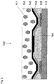
- Fig. 1 shows a schematic diagram of the structure of a conventional top-emitting device 100.
- the substrate 110 closest to the electrode 120 which is referred to below as the first electrode, designed as a reflective metal layer.
- the first electrode On the first electrode, a plurality of organic layers are applied, which is indicated in the figure as the organic layer structure 130.
- This layer structure comprises at least one organic electroluminescent layer.
- the layer structure 130 is followed by a second electrode 140, which consists of a transparent material, for example a conductive oxide.
- an exemplary emission point is designated by the numeral 131. Starting from this emission location Propagates the light, which is indicated in the figure with individual arrows. As can be seen, a reflection of the light and / or a transmission into the next layer takes place at the interfaces between two layers.
- organic mode The light which remains inside the component, here within the layer structure 130 and / or the electrode 140 (beam OM1) is referred to as organic mode
- the light leaving the component (beams EM1, EM2) is referred to as external modes. Since the organic layers also have an absorption coefficient not equal to 0 for the light generated within the layers, this is absorbed in the course of the propagation in the longitudinal direction of the layer.
- the invention uses such a design of the OLED, that in a top-emitting device, the coupling-out efficiency is increased.
- an additional layer also referred to as coupling-out layer, is provided on the side of the second electrode, which has optically effective heterogeneities, such as scattering centers, these heterogeneities being arranged within the coupling-out layer.
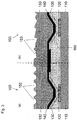
- Fig. 2 shown in a schematic diagram. Since the number of organic layers plays a minor role for the present invention, these are in Fig. 2 also indicated only as layer structure 130.
- an associated electrode 120 is applied, followed by the organic layer structure 130 connects, in which the light, usually in the visible range, is generated.
- the second electrode 140 is applied, to which, according to the invention, an additional layer, the coupling-out layer 150, is applied.
- inventive component can be produced in various ways depending on the embodiment.
- the decoupling layer produced in this way shows scattering properties without further additives, even solely due to intrinsic heterogeneities within the layer in the given order of magnitude.
- Another class of top-emitting electroluminescent devices according to the invention is produced in that the additional layer by one of the sputtering, PVD
- the additional layer Most of these materials listed for the additional layer are distinguished by their transparency in the visible spectral range by a refractive index which is greater than or equal to that of the organic layers.
- the light generated in the active organic layer is coupled in particularly effectively from the organic layers into the additional layer of the component according to the invention and from there is coupled out of the structure by the stated scattering centers. Since most of these materials of the additional layer are transparent in the visible spectral range but highly absorb in the UV range, such additional layers not only provide the organic layers with protection against moisture and air, but also also against UV radiation.
- the organic layers of the device can be damaged either by reaction with the plasma or mechanically.
- the uppermost organic layer of the diode for protecting the light-emitting layer is usually made particularly thick.
- the conductivity of this layer can be increased by doping.
- the transport layer has a thickness between 100 nm and 1 .mu.m, so that the active organic layer is protected below the transport layer in the subsequent process steps in particular the sputtering of the transparent electrode and / or the sputtering of the additional layer.
- the material of the additional layer such as ZnSe or GaN, is deposited from the gas phase, whereby the organic layers of the diode are charged much less, since in this manufacturing process, no gas plasma is needed.
- the respective material of the additional layer is applied by thermal evaporation in a vacuum on the transparent electrode. Typical evaporation temperatures are for example for ZnSe at 600 ° C to 800 ° C. In the vapor deposition process, the device is located at a sufficient distance from the heat source, so that there is no risk of thermal radiation for the organic layers of the layer structure. Again, the influence of heat on the OLED can be minimized by thick, doped transport layers.
- the incorporation of the scattering centers in the layer occurs automatically during vapor deposition from the gas phase due to the prevailing growth conditions for the additional layer. Since the device surface is not sufficiently smooth and has a temperature of RT, a monocrystalline smooth film can not grow, but for thermodynamic reasons, it does not come to a completely amorphous layer growth. The growth conditions lead to a clumping of polycrystalline microstructures on growth nuclei which grow together over time into a closed layer. This results in dislocation limits of the individual microcrystalline regions, whereby the desired optical heterogeneities are formed in the form of scattering centers. These dislocation limits are particularly pronounced in the direction of growth and lead to the desired scattering of the coupled into the additional layer of light.
- the separation of the additional or decoupling layer into individual microcrystalline domains can be further enhanced by alternately depositing different II-VI materials such as ZnSe and CdS or Group III nitrides such as GaN and AlN. These clump due to their different lattice structure preferably in separate crystal domains and in addition have different refractive indices, so that in this way particularly effective optical heterogeneities are formed.
- II-VI materials such as ZnSe and CdS or Group III nitrides such as GaN and AlN.
- the scattering particles are achieved in the additional layer by alternately sputtering the material of the additional layer and applying micro-metal particles by means of cold spray methods.
- a metal powder for example copper powder
- the additional layer is contained with optical heterogeneities produced by sputtering the additional layer material and a metal such as copper alternately onto the device.
- the metal is sputtered only very short, so that only metal clusters are formed, but no continuous metal film that would absorb too much.
- organic layers for forming the decoupling layer are vapor-deposited
- clusters of semiconductor compounds are evaporated between the organic layers.
- organic materials are chosen to produce the scattering centers in the coupling-out layer, which crystallize even polycrystalline.
- the additional layer is formed, for example, by anthracene, phthalocyanines, terphenyl diamines (TPD), perylenetetracarboxylic dianhydrides (PTCDA) or BPhen.
- the additional layer is produced by vapor deposition of organic layers and subsequent polymerization, for example by UV irradiation.
- Additional scattering centers in the form of micro-metal particles or metal oxide clusters can in turn be introduced into the coupling-out layer via a cold spray process or metal sputtering.
- an additional layer of methyl methacrylate (MMA) is indicated, which is polymerized after the introduction of the scattering particles by irradiation with UV light to Plexiglas (PMMA).
- MMA methyl methacrylate
- PMMA Plexiglas
- Fig. 3 a / b shows embodiments of a non-inventive top-emitting, electroluminescent device with a coupling-out layer whose surface facing away from the second electrode is structured.
- the configuration of the substrate 110, the first electrode 120, the organic layer structure 130, and the second electrode 140 is identical to that in FIG Fig. 2 shown example.
- the structuring of the surface is in the case of in Fig. 3a in a side view embodiment shown by a uniform juxtaposition of symmetrical Ridges 152 are provided on the surface of the outcoupling layer 150.
- This structuring is in the in Fig. 3a illustrated embodiment has been produced by brushing the additional layer in a direction perpendicular to the plane of the drawing.
- the structuring of the surface can also be designed in the form of cavities or recesses, wherein the structuring can be designed both one-dimensional, ie linear and two-dimensional.
- FIG. 3b The unclaimed embodiment shown in FIG. 1 has structuring of the surface of the additional layer 150 that is not uniform but includes randomly distributed and shaped cutouts or recesses 153 created by a grinding process.
- Fig. 4 shows a schematic diagram of the unclaimed structuring of the additional layer 150 by means of a punch 170, which has a plurality of equally spaced cutting edges 171, which are formed by two tapered surfaces 172, 173.
- the additional layer 150 is applied to the second electrode 140 and subsequently with the in the FIG. 4 structured process step on its surface.
- the stamp 170 described is placed on the surface of the additional layer 150 and pressed with a predetermined stamping force S in this. Due to the specified configuration of the cutting edges 171, a course of forces as indicated by the arrows F1, F2 is produced in the additional layer 150.
- the surface of the decoupling layer 150 is structured by a plurality of equally spaced grooves, since the cleavage of the additional layer is irreversible on the surface. These grooves or Their boundary surfaces form according to the optically active heterogeneities.
- additional separators 180 are integrated in the component, which prevent the serving as a molding die 170 causes up to the organic layer structure into deformations or damage.
- additional separators 180 for example, photoresist or of SiO 2
- these separators 180 present in the displays are designed for use in the present invention only to withstand the molding process with the molding tool 170 in terms of dimensional and stability.
- FIG. 12 shows a similar unclaimed embodiment of the invention showing a lighting application device of the present invention in which spacers 190 are inserted to prevent damage to the organic layer structure 130.
- the spacers must be mechanically designed to withstand the mechanical stress of the embossing process to produce the optically active heterogeneities in the outer surface of the additional layer.
- the stamping of wet-chemically prepared coupling-out layers takes place, depending on the embodiment, before, during or after the curing of the layer. In the former case, the mechanical stress for the organic layer structure is lowest.
- a gentle unclaimed method in structuring the additional layer is carried out by means of a technique similar to the screen printing method.
- first of all one of the abovementioned wet-chemically produced layers is applied to the second electrode of the component and this is structured by applying and pressing on a fabric.
- the common screen printing method doctoring for example using polyurethane doctor blades use.
- a further layer is wet-chemically spread through the fabric, causing a dissolution of the underlying layer and thus facilitates the structuring. In all cases, it must be ensured that the deformation persists permanently even after curing of the coupling-out layer.
- the roughening of the coupling-out layer takes place before it is applied to the component.
- the mechanical, thermal, radiative and / or chemical stress of the device can be significantly reduced.
- This advantageous method is achieved, for example, by laminating a prestructured laminating film.
- a transparent or semitransparent laminating film is processed from one of the abovementioned solvent materials.
- This is subsequently structured on its surface with one of the abovementioned mechanical or nonmechanical methods in such a way that its front side is roughened, whereby the
- the lamination of the film on the device is carried out so that the smooth back is connected to the device, usually with the second electrode.
- the lamination film is made of polyvinyl acetate, which is roughened by grinding and then smoothed on the transparent electrode, i. the top electrode is laminated or glued. With a component produced in this way, the efficiency increases by up to 300%.
- the additional layer is glued in the form of a pre-structured film by means of an adhesive on the smooth side of the transparent top electrode of the device.
- the adhesive is highly transparent and its properties are such that it encapsulates the organic layers well. This provides a sufficiently good protection against environmental influences, also can be dispensed with an additional encapsulation of the OLED.
- the structuring of the film may have different shapes; it is particularly advantageous to form a structuring of the film with roof-shaped strips and a height between 1 ⁇ m and 100 ⁇ m.
- the structuring can also be flat, for example by pyramidal structures.
- the decoupling layer is vapor-deposited on the transparent top electrode as an organic layer of Bphen.
- the scattering centers in the outcoupling layer are formed by partially decomposing Bphen itself.
- an additional encapsulation with a thin glass pane is provided. To avoid an influence of this glass on the light extraction is the
- Encapsulation glass pane attached at a sufficient distance from the decoupling layer, so that the glass only acts as a plane-parallel plate.
Landscapes
- Physics & Mathematics (AREA)
- Optics & Photonics (AREA)
- Electroluminescent Light Sources (AREA)
Applications Claiming Priority (2)
| Application Number | Priority Date | Filing Date | Title |
|---|---|---|---|
| DE102004035965A DE102004035965B4 (de) | 2004-07-23 | 2004-07-23 | Top-emittierendes, elektrolumineszierendes Bauelement mit zumindest einer organischen Schicht |
| PCT/DE2005/001229 WO2006010355A2 (de) | 2004-07-23 | 2005-07-12 | Top-emittierendes, elektrolumineszierendes bauelement mit zumindest einer organischen schicht |
Publications (2)
| Publication Number | Publication Date |
|---|---|
| EP1771895A2 EP1771895A2 (de) | 2007-04-11 |
| EP1771895B1 true EP1771895B1 (de) | 2016-06-08 |
Family
ID=35786553
Family Applications (1)
| Application Number | Title | Priority Date | Filing Date |
|---|---|---|---|
| EP05778553.7A Ceased EP1771895B1 (de) | 2004-07-23 | 2005-07-12 | Top-emittierendes, elektrolumineszierendes bauelement mit zumindest einer organischen schicht |
Country Status (8)
| Country | Link |
|---|---|
| US (1) | US8022619B2 (enExample) |
| EP (1) | EP1771895B1 (enExample) |
| JP (1) | JP5043658B2 (enExample) |
| KR (1) | KR101081710B1 (enExample) |
| CN (1) | CN101019250A (enExample) |
| DE (1) | DE102004035965B4 (enExample) |
| TW (1) | TWI292678B (enExample) |
| WO (1) | WO2006010355A2 (enExample) |
Families Citing this family (47)
| Publication number | Priority date | Publication date | Assignee | Title |
|---|---|---|---|---|
| US7540978B2 (en) | 2004-08-05 | 2009-06-02 | Novaled Ag | Use of an organic matrix material for producing an organic semiconductor material, organic semiconductor material and electronic component |
| DE102004042461A1 (de) * | 2004-08-31 | 2006-03-30 | Novaled Gmbh | Top-emittierendes, elektrolumineszierendes Bauelement mit Frequenzkonversionszentren |
| DE502005009415D1 (de) | 2005-05-27 | 2010-05-27 | Novaled Ag | Transparente organische Leuchtdiode |
| EP1729346A1 (de) * | 2005-06-01 | 2006-12-06 | Novaled AG | Lichtemittierendes Bauteil mit einer Elektrodenanordnung |
| EP1739765A1 (de) * | 2005-07-01 | 2007-01-03 | Novaled AG | Organische Leuchtdiode und Anordnung mit mehreren organischen Leuchtdioden |
| EP1808909A1 (de) * | 2006-01-11 | 2007-07-18 | Novaled AG | Elekrolumineszente Lichtemissionseinrichtung |
| DE102006051746A1 (de) * | 2006-09-29 | 2008-04-03 | Osram Opto Semiconductors Gmbh | Optoelektronisches Bauelement mit einer Lumineszenzkonversionsschicht |
| JP5239145B2 (ja) * | 2006-10-16 | 2013-07-17 | 凸版印刷株式会社 | 光学用部品およびその製造方法 |
| JP2008108439A (ja) * | 2006-10-23 | 2008-05-08 | Nec Lighting Ltd | 電界発光素子および電界発光パネル |
| DE102007006348A1 (de) * | 2006-12-22 | 2008-06-26 | Osram Opto Semiconductors Gmbh | Strahlungsemittierendes Bauelement |
| US20090051278A1 (en) * | 2007-08-21 | 2009-02-26 | Fujifilm Corporation | Organic electroluminescent display device having scattering member |
| DE102007044597A1 (de) * | 2007-09-19 | 2009-04-02 | Osram Opto Semiconductors Gmbh | Optoelektronisches Bauteil |
| DE102007062040B8 (de) * | 2007-12-21 | 2021-11-18 | Osram Oled Gmbh | Strahlungsemittierende Vorrichtung |
| JP5568224B2 (ja) * | 2008-07-04 | 2014-08-06 | ユー・ディー・シー アイルランド リミテッド | 有機エレクトロルミネッセンス素子 |
| DE102008056370B4 (de) * | 2008-11-07 | 2021-09-30 | Osram Oled Gmbh | Verfahren zur Herstellung eines organischen strahlungsemittierenden Bauelements und organisches strahlungsemittierendes Bauelement |
| DE102009030101A1 (de) * | 2008-12-08 | 2010-07-15 | Center For Abrasives And Refractories Research & Development C.A.R.R.D. Gmbh | Verschleißschutzschicht auf Basis einer Kunstharzmatrix, Verfahren zu ihrer Herstellung sowie ihre Verwendung |
| KR100989133B1 (ko) * | 2009-01-07 | 2010-10-20 | 삼성모바일디스플레이주식회사 | 유기 발광 표시 장치 |
| KR20100081772A (ko) * | 2009-01-07 | 2010-07-15 | 삼성모바일디스플레이주식회사 | 유기 발광 표시 장치 |
| KR101147428B1 (ko) * | 2009-02-09 | 2012-05-23 | 삼성모바일디스플레이주식회사 | 유기 발광 표시 장치 |
| DE102009025123A1 (de) * | 2009-06-16 | 2010-12-23 | Osram Opto Semiconductors Gmbh | Strahlungsemittierende Vorrichtung |
| WO2011010582A1 (ja) * | 2009-07-23 | 2011-01-27 | コニカミノルタホールディングス株式会社 | シート状構造体とその製造方法およびそれを用いた面発光体 |
| DE102009036134A1 (de) | 2009-08-05 | 2011-02-10 | Schott Ag | Substratglas für Lumineszenzdioden mit einer Streupartikel enthaltenden Schicht und Verfahren zu dessen Herstellung |
| JP5297991B2 (ja) | 2009-12-11 | 2013-09-25 | 株式会社日立製作所 | 有機発光ダイオード及びこれを用いた光源装置 |
| KR101663840B1 (ko) * | 2010-03-01 | 2016-10-07 | 가부시키가이샤 제이올레드 | 유기 el 장치 및 그 제조 방법 |
| US8237174B2 (en) * | 2010-05-10 | 2012-08-07 | National Central University | LED structure |
| JP5986992B2 (ja) * | 2010-06-14 | 2016-09-06 | ノヴァレッド ゲーエムベーハー | 有機発光素子 |
| US8637858B2 (en) | 2010-09-24 | 2014-01-28 | Novaled Ag | Tandem white OLED |
| JP6062636B2 (ja) * | 2011-03-10 | 2017-01-18 | ローム株式会社 | 有機el装置 |
| TWI451611B (zh) * | 2011-05-19 | 2014-09-01 | Au Optronics Corp | 有機發光裝置 |
| DE102011076750A1 (de) | 2011-05-31 | 2012-12-06 | Osram Opto Semiconductors Gmbh | Optoelektronisches Bauelement und Verfahren zum Herstellen eines optoelektronischen Bauelements |
| KR101829890B1 (ko) | 2011-12-23 | 2018-02-20 | 삼성디스플레이 주식회사 | 유기 발광 표시 장치 및 유기 발광 표시 장치 제조 방법 |
| DE102012207151A1 (de) * | 2012-04-30 | 2013-10-31 | Osram Opto Semiconductors Gmbh | Organisches lichtemittierendes bauelement und verfahren zur herstellung eines organischen lichtemittierenden bauelements |
| CN102709489B (zh) * | 2012-05-31 | 2015-10-21 | 昆山维信诺显示技术有限公司 | 高折射率散射层的制备方法及高出光效率的oled制备方法 |
| DE102012105810B4 (de) * | 2012-07-02 | 2020-12-24 | Heliatek Gmbh | Transparente Elektrode für optoelektronische Bauelemente |
| WO2014006565A2 (de) | 2012-07-02 | 2014-01-09 | Heliatek Gmbh | Transparente elektrode für optoelektronische bauelemente |
| DE102013108039A1 (de) | 2013-07-26 | 2015-01-29 | Osram Opto Semiconductors Gmbh | Strahlungsemittierende Vorrichtung |
| DE102013111736B4 (de) * | 2013-10-24 | 2024-11-07 | Pictiva Displays International Limited | Organische lichtemittierende Diode und Verfahren zum Herstellen einer organischen lichtemittierenden Diode |
| DE102013221991A1 (de) * | 2013-10-29 | 2015-04-30 | Fraunhofer-Gesellschaft zur Förderung der angewandten Forschung e.V. | Elektro-optisches, organisches Halbleiterbauelement mit voneinander beabstandeten Elektroden |
| EP2897186B1 (de) * | 2014-01-21 | 2018-12-26 | Covestro Deutschland AG | UV-Schutzfolie für OLEDs |
| US9843012B2 (en) | 2014-12-26 | 2017-12-12 | Industrial Technology Research Institute | Top emitting organic electroluminescent devices |
| TWI599556B (zh) * | 2015-07-03 | 2017-09-21 | 友達光電股份有限公司 | 有機發光元件 |
| KR102368894B1 (ko) * | 2016-09-30 | 2022-03-02 | 코오롱인더스트리 주식회사 | 광확산 기능을 부여한 봉지층 조성물 및 이를 이용하여 제조된 유기발광소자 |
| CN110098345B (zh) * | 2019-04-17 | 2020-11-06 | 深圳市华星光电半导体显示技术有限公司 | 有机发光二极管显示器及其制造方法 |
| CN110137383A (zh) * | 2019-06-24 | 2019-08-16 | 昆山国显光电有限公司 | 一种显示面板和显示面板的制作方法 |
| DE102020215067A1 (de) | 2020-11-30 | 2022-06-02 | Robert Bosch Gesellschaft mit beschränkter Haftung | Anzeigeeinrichtung zum Anzeigen zumindest eines Bildes, Verfahren zum Herstellen einer Anzeigeeinrichtung und Verfahren zum Betreiben einer Anzeigeeinrichtung |
| CN113097410A (zh) * | 2021-03-19 | 2021-07-09 | 深圳市华星光电半导体显示技术有限公司 | 显示面板及其制作方法、显示装置 |
| CN113871546A (zh) * | 2021-09-16 | 2021-12-31 | 深圳市华星光电半导体显示技术有限公司 | Oled显示面板及其制作方法、发光装置 |
Family Cites Families (38)
| Publication number | Priority date | Publication date | Assignee | Title |
|---|---|---|---|---|
| JP3203227B2 (ja) | 1998-02-27 | 2001-08-27 | 三洋電機株式会社 | 表示装置の製造方法 |
| JP2000075836A (ja) | 1998-09-02 | 2000-03-14 | Sharp Corp | 有機el発光装置とその駆動方法 |
| JP3640578B2 (ja) * | 1998-09-14 | 2005-04-20 | 株式会社オプテク | 有機半導体レーザ |
| JP2000196140A (ja) * | 1998-12-28 | 2000-07-14 | Sharp Corp | 有機エレクトロルミネッセンス素子とその製造法 |
| JP2000196410A (ja) * | 1998-12-31 | 2000-07-14 | Kazuhiko Yamanouchi | 高安定高結合弾性表面波基板とそれを用いた弾性表面波フィルタ及び弾性表面波機能素子 |
| JP3368225B2 (ja) * | 1999-03-11 | 2003-01-20 | キヤノン株式会社 | 回折光学素子の製造方法 |
| WO2000076008A1 (en) * | 1999-06-09 | 2000-12-14 | Cambridge Display Technology Limited | Method of producing organic light-emissive devices |
| JP2001052871A (ja) * | 1999-08-04 | 2001-02-23 | Toray Ind Inc | 有機電界発光装置 |
| JP2001148292A (ja) | 1999-09-08 | 2001-05-29 | Denso Corp | 有機el素子 |
| US7233026B2 (en) * | 2000-03-23 | 2007-06-19 | Emagin Corporation | Light extraction from color changing medium layers in organic light emitting diode devices |
| US6777871B2 (en) * | 2000-03-31 | 2004-08-17 | General Electric Company | Organic electroluminescent devices with enhanced light extraction |
| GB2361356B (en) | 2000-04-14 | 2005-01-05 | Seiko Epson Corp | Light emitting device |
| US7525165B2 (en) | 2000-04-17 | 2009-04-28 | Semiconductor Energy Laboratory Co., Ltd. | Light emitting device and manufacturing method thereof |
| TW516164B (en) * | 2000-04-21 | 2003-01-01 | Semiconductor Energy Lab | Self-light emitting device and electrical appliance using the same |
| TWI251089B (en) * | 2000-06-19 | 2006-03-11 | Nitto Denko Corp | Polarizer, polarizing plate, and liquid crystal display using the same |
| US6840999B2 (en) * | 2000-07-25 | 2005-01-11 | Board Of Regents The University Of Texas System | In situ regrowth and purification of crystalline thin films |
| KR20030072349A (ko) | 2000-11-02 | 2003-09-13 | 쓰리엠 이노베이티브 프로퍼티즈 컴파니 | 방사 디스플레이의 휘도 증대 |
| JP2004513483A (ja) * | 2000-11-02 | 2004-04-30 | スリーエム イノベイティブ プロパティズ カンパニー | 明るさおよびコントラスト増強直視型発光型ディスプレイ |
| US6933673B2 (en) | 2001-04-27 | 2005-08-23 | Semiconductor Energy Laboratory Co., Ltd. | Luminescent device and process of manufacturing the same |
| US6789835B2 (en) * | 2001-07-11 | 2004-09-14 | Harley-Davidson Motor Company Group, Inc. | Motorcycle windshield assembly |
| JP4152665B2 (ja) | 2001-07-11 | 2008-09-17 | 株式会社半導体エネルギー研究所 | 発光装置及びその作製方法 |
| US6734457B2 (en) | 2001-11-27 | 2004-05-11 | Semiconductor Energy Laboratory Co., Ltd. | Light emitting device |
| US7141817B2 (en) | 2001-11-30 | 2006-11-28 | Semiconductor Energy Laboratory Co., Ltd. | Light emitting device |
| DE10164016B4 (de) * | 2001-12-28 | 2020-01-23 | Osram Opto Semiconductors Gmbh | Organische Leuchtdiode (OLED) und Verfahren zu ihrer Herstellung |
| US7012363B2 (en) * | 2002-01-10 | 2006-03-14 | Universal Display Corporation | OLEDs having increased external electroluminescence quantum efficiencies |
| DE10215210B4 (de) | 2002-03-28 | 2006-07-13 | Novaled Gmbh | Transparentes, thermisch stabiles lichtemittierendes Bauelement mit organischen Schichten |
| CN1666579A (zh) | 2002-05-08 | 2005-09-07 | 泽奥勒克斯公司 | 使用反馈增强型发光二极管的照明器件 |
| US6670772B1 (en) | 2002-06-27 | 2003-12-30 | Eastman Kodak Company | Organic light emitting diode display with surface plasmon outcoupling |
| US6965197B2 (en) * | 2002-10-01 | 2005-11-15 | Eastman Kodak Company | Organic light-emitting device having enhanced light extraction efficiency |
| JP2004153089A (ja) * | 2002-10-31 | 2004-05-27 | Toyoda Gosei Co Ltd | Iii族窒化物系化合物半導体発光素子及びその製造方法 |
| US7224532B2 (en) | 2002-12-06 | 2007-05-29 | Chevron U.S.A. Inc. | Optical uses diamondoid-containing materials |
| WO2004056839A1 (ja) * | 2002-12-19 | 2004-07-08 | Semiconductor Energy Laboratory Co., Ltd. | 有機金属錯体および前記有機金属錯体を用いた電界発光素子、並びに前記電界発光素子を用いた発光装置 |
| JP2004207136A (ja) * | 2002-12-26 | 2004-07-22 | Nitto Denko Corp | 面光源及びこれを用いた表示装置 |
| EP1606846B1 (en) | 2003-03-24 | 2010-10-27 | Konarka Technologies, Inc. | Photovoltaic cell with mesh electrode |
| KR20050066970A (ko) | 2003-12-26 | 2005-06-30 | 닛토덴코 가부시키가이샤 | 전자발광 장치, 이를 사용하는 면광원 및 디스플레이 |
| KR101097301B1 (ko) | 2005-02-05 | 2011-12-23 | 삼성모바일디스플레이주식회사 | 백색발광소자 |
| US7531955B2 (en) * | 2005-07-12 | 2009-05-12 | Eastman Kodak Company | OLED device with improved efficiency and robustness |
| DE502005005126D1 (de) | 2005-08-11 | 2008-10-02 | Novaled Ag | Verfahren zum Herstellen eines top-emittierenden Bauteils sowie Verwendung |
-
2004
- 2004-07-23 DE DE102004035965A patent/DE102004035965B4/de not_active Expired - Fee Related
-
2005
- 2005-07-12 WO PCT/DE2005/001229 patent/WO2006010355A2/de not_active Ceased
- 2005-07-12 EP EP05778553.7A patent/EP1771895B1/de not_active Ceased
- 2005-07-12 KR KR1020077003762A patent/KR101081710B1/ko not_active Expired - Fee Related
- 2005-07-12 JP JP2007521783A patent/JP5043658B2/ja not_active Expired - Fee Related
- 2005-07-12 CN CNA2005800243182A patent/CN101019250A/zh active Pending
- 2005-07-12 US US11/572,458 patent/US8022619B2/en not_active Expired - Fee Related
- 2005-07-14 TW TW094123978A patent/TWI292678B/zh not_active IP Right Cessation
Also Published As
| Publication number | Publication date |
|---|---|
| WO2006010355A2 (de) | 2006-02-02 |
| JP5043658B2 (ja) | 2012-10-10 |
| US20080048557A1 (en) | 2008-02-28 |
| CN101019250A (zh) | 2007-08-15 |
| US8022619B2 (en) | 2011-09-20 |
| WO2006010355A3 (de) | 2006-10-19 |
| TWI292678B (en) | 2008-01-11 |
| WO2006010355B1 (de) | 2006-12-14 |
| KR101081710B1 (ko) | 2011-11-09 |
| EP1771895A2 (de) | 2007-04-11 |
| TW200607388A (en) | 2006-02-16 |
| JP2008507809A (ja) | 2008-03-13 |
| DE102004035965B4 (de) | 2007-07-26 |
| DE102004035965A1 (de) | 2006-06-08 |
| KR20070044454A (ko) | 2007-04-27 |
Similar Documents
| Publication | Publication Date | Title |
|---|---|---|
| EP1771895B1 (de) | Top-emittierendes, elektrolumineszierendes bauelement mit zumindest einer organischen schicht | |
| DE102004041371B4 (de) | Bauelement auf Basis einer organischen Leuchtdiodeneinrichtung und Verfahren zur Herstellung | |
| DE102011086168B4 (de) | Organisches Licht emittierendes Bauelement und Verfahren zur Herstellung eines organischen optoelektronischen Bauelements | |
| KR100852110B1 (ko) | 유기 전계 발광 소자 및 그 제조 방법 | |
| DE10164016B4 (de) | Organische Leuchtdiode (OLED) und Verfahren zu ihrer Herstellung | |
| DE102007053286B4 (de) | Verfahren zur Herstellung eines optoelektronischen Bauelements | |
| JP2008507809A5 (enExample) | ||
| WO2010025696A2 (de) | Verfahren zur herstellung eines organischen strahlungsemittierenden bauelements und organisches strahlungsemittierendes bauelement | |
| DE102004042461A1 (de) | Top-emittierendes, elektrolumineszierendes Bauelement mit Frequenzkonversionszentren | |
| DE102013013129B4 (de) | Optoelektronisches Bauelement und Verfahren zur Herstellung eines optoelektronischen Bauelements | |
| WO2004025747A2 (de) | Organisches photovoltaisches bauelement und herstellungsverfahren dazu | |
| WO2004044999A2 (de) | Organische elektrolumineszente lichtquelle mit antireflexionsschicht | |
| EP2342771B1 (de) | Verfahren zur herstellung eines organischen strahlungsemittierenden bauelements | |
| DE102008051012B4 (de) | Lichtemittierende Vorrichtung und Verfahren zum Herstellen | |
| DE102008031531A1 (de) | Organisches strahlungsemittierendes Bauelement und Verfahren zur Herstellung eines organischen strahlungsemittierenden Bauelements | |
| EP2936583B1 (de) | Verfahren zum herstellen eines organischen lichtemittierenden bauelementes | |
| KR101570968B1 (ko) | 유기 발광소자용 기판, 그 제조방법 및 이를 구비하는 유기 발광소자 | |
| DE102015103702B4 (de) | Verfahren zum Herstellen eines optoelektronischen Bauelements | |
| DE102012109209A1 (de) | Verfahren zum Herstellen eines optoelektronischen Bauelements und optoelektronisches Bauelement | |
| WO2022063645A1 (de) | Verfahren zur herstellung von optoelektronischen halbleiterbauelementen und optoelektronisches halbleiterbauelement sowie eine optoelektronische anordnung | |
| DE102017106018A1 (de) | Verfahren zum herstellen eines optoelektronischen bauelements und ein optoelektronisches bauelement |
Legal Events
| Date | Code | Title | Description |
|---|---|---|---|
| PUAI | Public reference made under article 153(3) epc to a published international application that has entered the european phase |
Free format text: ORIGINAL CODE: 0009012 |
|
| 17P | Request for examination filed |
Effective date: 20070122 |
|
| AK | Designated contracting states |
Kind code of ref document: A2 Designated state(s): AT BE BG CH CY CZ DE DK EE ES FI FR GB GR HU IE IS IT LI LT LU LV MC NL PL PT RO SE SI SK TR |
|
| AX | Request for extension of the european patent |
Extension state: AL BA HR MK YU |
|
| RIN1 | Information on inventor provided before grant (corrected) |
Inventor name: VEHSE, MARTIN Inventor name: ROMAINCZYK, TILMANN Inventor name: BIRKNSTOCK, JAN |
|
| DAX | Request for extension of the european patent (deleted) | ||
| REG | Reference to a national code |
Ref country code: DE Ref legal event code: 8566 |
|
| RBV | Designated contracting states (corrected) |
Designated state(s): GB NL |
|
| 17Q | First examination report despatched |
Effective date: 20080818 |
|
| REG | Reference to a national code |
Ref country code: DE Ref legal event code: R079 Free format text: PREVIOUS MAIN CLASS: H01L0051000000 Ipc: H01L0051520000 |
|
| GRAP | Despatch of communication of intention to grant a patent |
Free format text: ORIGINAL CODE: EPIDOSNIGR1 |
|
| INTG | Intention to grant announced |
Effective date: 20150630 |
|
| RIC1 | Information provided on ipc code assigned before grant |
Ipc: H01L 51/52 20060101AFI20150622BHEP |
|
| GRAP | Despatch of communication of intention to grant a patent |
Free format text: ORIGINAL CODE: EPIDOSNIGR1 |
|
| INTG | Intention to grant announced |
Effective date: 20150812 |
|
| INTG | Intention to grant announced |
Effective date: 20151126 |
|
| GRAS | Grant fee paid |
Free format text: ORIGINAL CODE: EPIDOSNIGR3 |
|
| RIN1 | Information on inventor provided before grant (corrected) |
Inventor name: ROMAINCZYK, TILMANN Inventor name: VEHSE, MARTIN Inventor name: BIRKNSTOCK, JAN |
|
| GRAA | (expected) grant |
Free format text: ORIGINAL CODE: 0009210 |
|
| RAP1 | Party data changed (applicant data changed or rights of an application transferred) |
Owner name: NOVALED GMBH |
|
| AK | Designated contracting states |
Kind code of ref document: B1 Designated state(s): GB NL |
|
| REG | Reference to a national code |
Ref country code: GB Ref legal event code: FG4D Free format text: NOT ENGLISH |
|
| REG | Reference to a national code |
Ref country code: NL Ref legal event code: FP |
|
| PLBE | No opposition filed within time limit |
Free format text: ORIGINAL CODE: 0009261 |
|
| STAA | Information on the status of an ep patent application or granted ep patent |
Free format text: STATUS: NO OPPOSITION FILED WITHIN TIME LIMIT |
|
| 26N | No opposition filed |
Effective date: 20170309 |
|
| PGFP | Annual fee paid to national office [announced via postgrant information from national office to epo] |
Ref country code: GB Payment date: 20220526 Year of fee payment: 18 |
|
| P01 | Opt-out of the competence of the unified patent court (upc) registered |
Effective date: 20230515 |
|
| PGFP | Annual fee paid to national office [announced via postgrant information from national office to epo] |
Ref country code: NL Payment date: 20230525 Year of fee payment: 19 |
|
| GBPC | Gb: european patent ceased through non-payment of renewal fee |
Effective date: 20230712 |
|
| PG25 | Lapsed in a contracting state [announced via postgrant information from national office to epo] |
Ref country code: GB Free format text: LAPSE BECAUSE OF NON-PAYMENT OF DUE FEES Effective date: 20230712 |
|
| REG | Reference to a national code |
Ref country code: NL Ref legal event code: MM Effective date: 20240801 |
|
| PG25 | Lapsed in a contracting state [announced via postgrant information from national office to epo] |
Ref country code: NL Free format text: LAPSE BECAUSE OF NON-PAYMENT OF DUE FEES Effective date: 20240801 |