EP1771888B1 - NANOSCALE InP FET - Google Patents
NANOSCALE InP FET Download PDFInfo
- Publication number
- EP1771888B1 EP1771888B1 EP05759916A EP05759916A EP1771888B1 EP 1771888 B1 EP1771888 B1 EP 1771888B1 EP 05759916 A EP05759916 A EP 05759916A EP 05759916 A EP05759916 A EP 05759916A EP 1771888 B1 EP1771888 B1 EP 1771888B1
- Authority
- EP
- European Patent Office
- Prior art keywords
- source
- channel region
- region
- growth
- drain
- Prior art date
- Legal status (The legal status is an assumption and is not a legal conclusion. Google has not performed a legal analysis and makes no representation as to the accuracy of the status listed.)
- Expired - Lifetime
Links
Images
Classifications
-
- H—ELECTRICITY
- H10—SEMICONDUCTOR DEVICES; ELECTRIC SOLID-STATE DEVICES NOT OTHERWISE PROVIDED FOR
- H10D—INORGANIC ELECTRIC SEMICONDUCTOR DEVICES
- H10D30/00—Field-effect transistors [FET]
- H10D30/60—Insulated-gate field-effect transistors [IGFET]
-
- B—PERFORMING OPERATIONS; TRANSPORTING
- B82—NANOTECHNOLOGY
- B82Y—SPECIFIC USES OR APPLICATIONS OF NANOSTRUCTURES; MEASUREMENT OR ANALYSIS OF NANOSTRUCTURES; MANUFACTURE OR TREATMENT OF NANOSTRUCTURES
- B82Y10/00—Nanotechnology for information processing, storage or transmission, e.g. quantum computing or single electron logic
-
- B—PERFORMING OPERATIONS; TRANSPORTING
- B82—NANOTECHNOLOGY
- B82Y—SPECIFIC USES OR APPLICATIONS OF NANOSTRUCTURES; MEASUREMENT OR ANALYSIS OF NANOSTRUCTURES; MANUFACTURE OR TREATMENT OF NANOSTRUCTURES
- B82Y40/00—Manufacture or treatment of nanostructures
-
- H—ELECTRICITY
- H10—SEMICONDUCTOR DEVICES; ELECTRIC SOLID-STATE DEVICES NOT OTHERWISE PROVIDED FOR
- H10D—INORGANIC ELECTRIC SEMICONDUCTOR DEVICES
- H10D48/00—Individual devices not covered by groups H10D1/00 - H10D44/00
- H10D48/30—Devices controlled by electric currents or voltages
- H10D48/32—Devices controlled by only the electric current supplied, or only the electric potential applied, to an electrode which does not carry the current to be rectified, amplified or switched
- H10D48/36—Unipolar devices
-
- H—ELECTRICITY
- H10—SEMICONDUCTOR DEVICES; ELECTRIC SOLID-STATE DEVICES NOT OTHERWISE PROVIDED FOR
- H10D—INORGANIC ELECTRIC SEMICONDUCTOR DEVICES
- H10D62/00—Semiconductor bodies, or regions thereof, of devices having potential barriers
- H10D62/10—Shapes, relative sizes or dispositions of the regions of the semiconductor bodies; Shapes of the semiconductor bodies
- H10D62/117—Shapes of semiconductor bodies
- H10D62/118—Nanostructure semiconductor bodies
- H10D62/119—Nanowire, nanosheet or nanotube semiconductor bodies
- H10D62/121—Nanowire, nanosheet or nanotube semiconductor bodies oriented parallel to substrates
-
- H—ELECTRICITY
- H10—SEMICONDUCTOR DEVICES; ELECTRIC SOLID-STATE DEVICES NOT OTHERWISE PROVIDED FOR
- H10D—INORGANIC ELECTRIC SEMICONDUCTOR DEVICES
- H10D62/00—Semiconductor bodies, or regions thereof, of devices having potential barriers
- H10D62/80—Semiconductor bodies, or regions thereof, of devices having potential barriers characterised by the materials
- H10D62/85—Semiconductor bodies, or regions thereof, of devices having potential barriers characterised by the materials being Group III-V materials, e.g. GaAs
-
- Y—GENERAL TAGGING OF NEW TECHNOLOGICAL DEVELOPMENTS; GENERAL TAGGING OF CROSS-SECTIONAL TECHNOLOGIES SPANNING OVER SEVERAL SECTIONS OF THE IPC; TECHNICAL SUBJECTS COVERED BY FORMER USPC CROSS-REFERENCE ART COLLECTIONS [XRACs] AND DIGESTS
- Y10—TECHNICAL SUBJECTS COVERED BY FORMER USPC
- Y10S—TECHNICAL SUBJECTS COVERED BY FORMER USPC CROSS-REFERENCE ART COLLECTIONS [XRACs] AND DIGESTS
- Y10S438/00—Semiconductor device manufacturing: process
- Y10S438/962—Quantum dots and lines
-
- Y—GENERAL TAGGING OF NEW TECHNOLOGICAL DEVELOPMENTS; GENERAL TAGGING OF CROSS-SECTIONAL TECHNOLOGIES SPANNING OVER SEVERAL SECTIONS OF THE IPC; TECHNICAL SUBJECTS COVERED BY FORMER USPC CROSS-REFERENCE ART COLLECTIONS [XRACs] AND DIGESTS
- Y10—TECHNICAL SUBJECTS COVERED BY FORMER USPC
- Y10S—TECHNICAL SUBJECTS COVERED BY FORMER USPC CROSS-REFERENCE ART COLLECTIONS [XRACs] AND DIGESTS
- Y10S977/00—Nanotechnology
- Y10S977/70—Nanostructure
- Y10S977/762—Nanowire or quantum wire, i.e. axially elongated structure having two dimensions of 100 nm or less
-
- Y—GENERAL TAGGING OF NEW TECHNOLOGICAL DEVELOPMENTS; GENERAL TAGGING OF CROSS-SECTIONAL TECHNOLOGIES SPANNING OVER SEVERAL SECTIONS OF THE IPC; TECHNICAL SUBJECTS COVERED BY FORMER USPC CROSS-REFERENCE ART COLLECTIONS [XRACs] AND DIGESTS
- Y10—TECHNICAL SUBJECTS COVERED BY FORMER USPC
- Y10S—TECHNICAL SUBJECTS COVERED BY FORMER USPC CROSS-REFERENCE ART COLLECTIONS [XRACs] AND DIGESTS
- Y10S977/00—Nanotechnology
- Y10S977/70—Nanostructure
- Y10S977/813—Of specified inorganic semiconductor composition, e.g. periodic table group IV-VI compositions
- Y10S977/815—Group III-V based compounds, e.g. AlaGabIncNxPyAsz
- Y10S977/818—III-P based compounds, e.g. AlxGayIn2P
-
- Y—GENERAL TAGGING OF NEW TECHNOLOGICAL DEVELOPMENTS; GENERAL TAGGING OF CROSS-SECTIONAL TECHNOLOGIES SPANNING OVER SEVERAL SECTIONS OF THE IPC; TECHNICAL SUBJECTS COVERED BY FORMER USPC CROSS-REFERENCE ART COLLECTIONS [XRACs] AND DIGESTS
- Y10—TECHNICAL SUBJECTS COVERED BY FORMER USPC
- Y10S—TECHNICAL SUBJECTS COVERED BY FORMER USPC CROSS-REFERENCE ART COLLECTIONS [XRACs] AND DIGESTS
- Y10S977/00—Nanotechnology
- Y10S977/902—Specified use of nanostructure
- Y10S977/932—Specified use of nanostructure for electronic or optoelectronic application
- Y10S977/936—Specified use of nanostructure for electronic or optoelectronic application in a transistor or 3-terminal device
- Y10S977/938—Field effect transistors, FETS, with nanowire- or nanotube-channel region
Definitions
- the invention relates to a nanoscale FET, and in particular to a FET using nanowire and nanotube technology.
- MOS metal oxide semiconductor
- MIS metal insulator semiconductor
- US2003/0148562 proposes a field effect transistor with a carbon nanowire forming a source, channel and drain region and a surrounding nanotube gate.
- a boron nitride nanotube insulator is proposed as an insulator between the nanowire channel and the nanotube gate.
- the manufacture of such a device presents formidable manufacturing difficulties.
- US2003/0178617 presents self-aligned carbon nanowire structures, mostly using vertical nanowires but including in one embodiment horizontal nanowires formed with chemical groups, on the ends and then aligned by providing complimentary chemical groups where the nanowires are to be assembled. For example, complementary strands of DNA are said to make suitable complementary groups.
- US 2004/0036128 describes another carbon nano-structure, in this case using carbon nanotubes.
- the nanotubes are grown horizontally from drain catalyst contacts.
- VLS vapour-liquid-solid
- the low diameter clusters are created by laser ablation of a metal target which generates a suspension of metal clusters.
- the metal atoms may be for example of gold.
- a transistor device according to claim 1, and a method of manufacturing thereof according to claim 5.
- nanowire is reserved for solid wire nanostructures, i.e. is not used for hollow nanostructures, and the term nanotube is used for nanostructures with a hollow interior.
- the nanotube channel has thin walls and accordingly will, in use, be fully inverted and this gives rise to good transistor properties. Further, the fact that the channel is fully inverted can reduce the importance of misalignment and this can improve the manufacturability of the device.
- the thickness of the nanowire source and drain regions can be made larger in regions spaced away from the nanotube channel than adjacent to the nanotube channel to facilitate contacting the device, both improving manufacturability and improving the contact resistance by having a large contact area.
- the transistor is formed on a substrate having a first major surface; a plurality of said continuous nanostructures extend across the first major surface substantially parallel to one another in a longitudinal direction; a thin gate insulating layer extends laterally over the channel regions of the plurality of nanostructures; and a conductive gate material extends laterally over the thin gate insulating layer.
- substantially parallel is not intended to imply that the nanostructures need to be exactly straight or all precisely aligned, and some variation in direction either within a single nanostructure or between different nanostructures is acceptable.
- the channel region of the nanotube may be in the range 5 to 100 nm long.
- the wall thickness of the channel region of the nanotube may be in the range 2 to 20 nm.
- the transistion between the nanotube and nanowire regions may conveniently be made by varying the growth temperature. Accordingly, source and drain regions may be grown at a temperature below a predetermined transition temperature and the channel region at a temperature above the predetermined transition temperature. In the case of an InP nanotube the transition temperature may be 500 °C.
- the invention may include growing channel region of the nanostructure to have a first width and growing the source and drain regions to have a maximum width at least three times the first width.
- a particularly convenient method of providing a plurality of catalytic starting points includes:
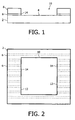
- a substrate 2 is provided having a first major surface 4, shown on top in Figure 1 .
- a silicon substrate is widely available and convenient.
- a thin gold layer is deposited on the substrate, and patterned to form a plurality of thin gold lines 6 running in parallel on the first major surface 4.
- An oxide layer 8 is deposited over the whole surface.
- a window 10 is then patterned and etched through both the oxide layer 8 and the gold lines 6 to expose the substrate 2 in the window.
- the window 10 is conveniently square or rectangular having opposed edges 12 running perpendicular to the gold lines 6.
- the ends 14 of the gold lines at the opposed edges form catalytic starting points for the growth of the nanostructures.
- InP nanostructures 18 are grown though the skilled person will be able to apply the technique to other materials as required.
- nanostructures as grown depend on the growth conditions and in particular the temperature.
- the initial growth is carried out using growth conditions to grow doped nanowire regions 20, without a hollow interior, of InP, and a diameter of order 20nm.
- such nanowire growth can be carried out at a temperature below 500°C.
- the growth conditions can be varied to provide a tapering region 22, either over the whole of the doped nanowire regions or alternatively only after an initial section of constant width. This can provide a wider nanowire in the regions to be contacted by the source and drain contacts than in the region adjacent to the channel.
- the dopant is removed and the temperature raised above 500°C, so that undoped nanotubes are grown to form a channel region 24.
- the length of the channel region may conveniently be of order 5 to 100nm, and the width of the nanotubes of order 20 to 100nm.
- the wall thickness may be 2 to 20nm
- the growth conditions are then changed again and growth continued to form doped nanowire regions 26.
- part of the region may be a tapering region 22.
- the second doped nanowire regions 26 can be formed using the same growth conditions as the first doped nanowire regions 20.
- the changes in the growth conditions can be sufficiently abrupt to create a very abrupt boundary between the channel region 24 and surrounding doped regions 20,26, and the doping in the source and drain can also be readily controlled.
- a VLS method may be used in which the substrate is placed on a temperature controlled alumina block and the substrate temperature stabilised. Then, a beam of an ArF laser is focussed on an InP target to vaporise InP which grows on the gold catalyst.
- the transition temperature of the transition between nanowire and nanotube growth is 500°C for undoped InP but varies a little for doped InP.
- a growth temperature of 485°C or less grows nanowires and a temperature of above 530°C grows tubes.
- a growth temperature of 480°C grows nanotubes.
- Zn doping a temperature of less than 480°C grows a solid nanowire, and a temperature of greater than 515°C grows nanotubes.
- nanotubes with a wall thickness of 2nm and a diameter or 27 nm were grown.
- the wall thickness of the nanotubes can be varied by varying the growth temperature above the transition temperature. In general, a higher temperature is used to grow thinner walls. For example, for an InP target doped with 0.1% S, variation of the substrate temperature from 480°C to 550°C resulted in the wall thickness changing from about 14nm to 9nm respectively.
- nanostructure growth will in fact commence from both opposed edges 12 of the window 10, although this is largely irrelevant in view of the symmetrical nature of the nanostructures.
- a thin dielectric layer 30 is laid over the channel regions 24 of the nanostructures 18.
- this is a thin layer of silicon dioxide.
- a gate material 32 is then deposited over the surface.
- the gate material is of metal though polysilicon may also be used.
- Gate 32 patterning then follows. Contacts, including source contact 34 and drain contact 36, are then made to the doped regions.
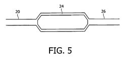
- Figure 5 is an illustrative section view of the nanostructure formed showing the central nanotube region 24 with thin walls and the end source and drain regions 20,26 which are filled.
- the patterning steps may use electron beam lithography, though deep ultraviolet (DUV) or especially extreme ultraviolet (EUV) lithography may also be used.
- DUV deep ultraviolet
- EUV extreme ultraviolet
- the advantages of the device architecture include a device architecture with many degrees of freedom that can be implemented in a variety of materials, with different source drain doping and a variety of dimensions to enable the devices to be tailored to various requirements.
- the whole nanostructure can be grown in a single process.
- the very narrow channel region can be sufficiently small so that quantum effects increase the mobility.
- the channel can be fully inverted, which can avoid problems caused by gate misalignment thereby making the device more manufactureable.
- Both NMOS and PMOS devices can be manufactured in high mobility materials using the invention.
- dopant activation energies and transitions can be tuned to obtain a single atom abruptness from doped regions 20, 26 to the undoped channel region 24.
- InP Indium gallium arsphide
- Ge Ge
- GaN GaN
- group III-V, II-VI and IV semiconductors indeed all group III-V, II-VI and IV semiconductors, or ternary or quaternary semiconductors.
- the gate can be deposited all around the channel regions 24 leading to improved performance.
Landscapes
- Engineering & Computer Science (AREA)
- Nanotechnology (AREA)
- Chemical & Material Sciences (AREA)
- Crystallography & Structural Chemistry (AREA)
- Physics & Mathematics (AREA)
- Theoretical Computer Science (AREA)
- Mathematical Physics (AREA)
- Condensed Matter Physics & Semiconductors (AREA)
- General Physics & Mathematics (AREA)
- Manufacturing & Machinery (AREA)
- Thin Film Transistor (AREA)
- Insulated Gate Type Field-Effect Transistor (AREA)
- Element Separation (AREA)
Applications Claiming Priority (2)
| Application Number | Priority Date | Filing Date | Title |
|---|---|---|---|
| GBGB0415891.1A GB0415891D0 (en) | 2004-07-16 | 2004-07-16 | Nanoscale fet |
| PCT/IB2005/052313 WO2006008703A2 (en) | 2004-07-16 | 2005-07-12 | Nanoscale fet |
Publications (2)
| Publication Number | Publication Date |
|---|---|
| EP1771888A2 EP1771888A2 (en) | 2007-04-11 |
| EP1771888B1 true EP1771888B1 (en) | 2011-09-14 |
Family
ID=32893646
Family Applications (1)
| Application Number | Title | Priority Date | Filing Date |
|---|---|---|---|
| EP05759916A Expired - Lifetime EP1771888B1 (en) | 2004-07-16 | 2005-07-12 | NANOSCALE InP FET |
Country Status (7)
| Country | Link |
|---|---|
| US (1) | US7838368B2 (enExample) |
| EP (1) | EP1771888B1 (enExample) |
| JP (1) | JP2008507127A (enExample) |
| CN (1) | CN100521237C (enExample) |
| AT (1) | ATE524831T1 (enExample) |
| GB (1) | GB0415891D0 (enExample) |
| WO (1) | WO2006008703A2 (enExample) |
Families Citing this family (12)
| Publication number | Priority date | Publication date | Assignee | Title |
|---|---|---|---|---|
| US7858918B2 (en) * | 2007-02-05 | 2010-12-28 | Ludwig Lester F | Molecular transistor circuits compatible with carbon nanotube sensors and transducers |
| US7838809B2 (en) | 2007-02-17 | 2010-11-23 | Ludwig Lester F | Nanoelectronic differential amplifiers and related circuits having carbon nanotubes, graphene nanoribbons, or other related materials |
| US8389387B2 (en) * | 2009-01-06 | 2013-03-05 | Brookhaven Science Associates, Llc | Segmented nanowires displaying locally controllable properties |
| US8890115B2 (en) * | 2009-01-06 | 2014-11-18 | Brookhaven Science Associates, Llc | Stable and metastable nanowires displaying locally controllable properties |
| CN104137228A (zh) * | 2011-12-23 | 2014-11-05 | 英特尔公司 | 具有环绕式接触部的纳米线结构 |
| EP2741337B1 (en) * | 2012-12-07 | 2018-04-11 | IMEC vzw | Semiconductor heterostructure field effect transistor and method for making thereof |
| WO2014179340A2 (en) * | 2013-04-29 | 2014-11-06 | The University Of North Carolina At Chapel Hill | Methods and systems for chemically encoding high-resolution shapes in silicon nanowires |
| US9741811B2 (en) | 2014-12-15 | 2017-08-22 | Samsung Electronics Co., Ltd. | Integrated circuit devices including source/drain extension regions and methods of forming the same |
| CN105990413B (zh) * | 2015-02-06 | 2020-11-17 | 联华电子股份有限公司 | 具有纳米线结构的半导体结构与制造方法 |
| CN105789442B (zh) * | 2016-05-23 | 2018-12-18 | 京东方科技集团股份有限公司 | 一种薄膜晶体管、其制作方法及相应装置 |
| US11004985B2 (en) * | 2016-05-30 | 2021-05-11 | Samsung Electronics Co., Ltd. | Semiconductor device having multi-thickness nanowire |
| CN119545838B (zh) * | 2024-11-26 | 2025-09-16 | 北京智芯微电子科技有限公司 | 环栅场效应晶体管及其制备方法、芯片和电子设备 |
Family Cites Families (8)
| Publication number | Priority date | Publication date | Assignee | Title |
|---|---|---|---|---|
| JP4112358B2 (ja) | 2000-07-04 | 2008-07-02 | インフィネオン テクノロジーズ アクチエンゲゼルシャフト | 電界効果トランジスタ |
| GB2382718B (en) | 2000-07-18 | 2004-03-24 | Lg Electronics Inc | Field effect transistor using horizontally grown carbon nanotubes |
| JP3859199B2 (ja) * | 2000-07-18 | 2006-12-20 | エルジー エレクトロニクス インコーポレイティド | カーボンナノチューブの水平成長方法及びこれを利用した電界効果トランジスタ |
| KR101008294B1 (ko) * | 2001-03-30 | 2011-01-13 | 더 리전트 오브 더 유니버시티 오브 캘리포니아 | 나노구조체 및 나노와이어의 제조 방법 및 그로부터 제조되는 디바이스 |
| AU2003215840A1 (en) * | 2002-03-28 | 2003-10-13 | Koninklijke Philips Electronics N.V. | Nanowire and electronic device |
| US7115916B2 (en) * | 2002-09-26 | 2006-10-03 | International Business Machines Corporation | System and method for molecular optical emission |
| CN100459181C (zh) * | 2002-11-05 | 2009-02-04 | 皇家飞利浦电子股份有限公司 | 纳米结构、具有这种纳米结构的电子器件和纳米结构的制造方法 |
| US7180107B2 (en) * | 2004-05-25 | 2007-02-20 | International Business Machines Corporation | Method of fabricating a tunneling nanotube field effect transistor |
-
2004
- 2004-07-16 GB GBGB0415891.1A patent/GB0415891D0/en not_active Ceased
-
2005
- 2005-07-12 CN CNB2005800239721A patent/CN100521237C/zh not_active Expired - Fee Related
- 2005-07-12 AT AT05759916T patent/ATE524831T1/de not_active IP Right Cessation
- 2005-07-12 US US11/632,738 patent/US7838368B2/en active Active
- 2005-07-12 EP EP05759916A patent/EP1771888B1/en not_active Expired - Lifetime
- 2005-07-12 JP JP2007520958A patent/JP2008507127A/ja not_active Withdrawn
- 2005-07-12 WO PCT/IB2005/052313 patent/WO2006008703A2/en not_active Ceased
Also Published As
| Publication number | Publication date |
|---|---|
| EP1771888A2 (en) | 2007-04-11 |
| US7838368B2 (en) | 2010-11-23 |
| WO2006008703A2 (en) | 2006-01-26 |
| JP2008507127A (ja) | 2008-03-06 |
| US20070262397A1 (en) | 2007-11-15 |
| WO2006008703A3 (en) | 2006-06-22 |
| ATE524831T1 (de) | 2011-09-15 |
| CN1985378A (zh) | 2007-06-20 |
| GB0415891D0 (en) | 2004-08-18 |
| CN100521237C (zh) | 2009-07-29 |
Similar Documents
| Publication | Publication Date | Title |
|---|---|---|
| US7858965B2 (en) | Nanowire heterostructures | |
| TWI463654B (zh) | 奈米管/奈米導線場效電晶體之自行對準製程 | |
| US7230286B2 (en) | Vertical FET with nanowire channels and a silicided bottom contact | |
| Lauhon et al. | Epitaxial core–shell and core–multishell nanowire heterostructures | |
| EP2309544B1 (en) | Tunnel field effect transistor with improved subthreshold swing | |
| EP1661173B1 (en) | Method of fabricating an ultra-narrow channel semiconductor device | |
| US8080468B2 (en) | Methods for fabricating passivated silicon nanowires and devices thus obtained | |
| EP1979946B1 (en) | Nanowire tunneling transistor | |
| US20110233512A1 (en) | Vertical integrated silicon nanowire field effect transistors and methods of fabrication | |
| US8313990B2 (en) | Nanowire FET having induced radial strain | |
| EP1771888B1 (en) | NANOSCALE InP FET | |
| US7629629B2 (en) | Semiconductor nanowire and semiconductor device including the nanowire | |
| CN101807668A (zh) | 碳纳米管场效应晶体管半导体器件及其制造方法 | |
| KR20080096791A (ko) | 장벽 영역을 포함하는 트랜지스터 | |
| KR20060117692A (ko) | 실리콘 나노와이어 기판 및 그 제조방법, 그리고 이를이용한 박막 트랜지스터의 제조방법 | |
| KR100834896B1 (ko) | 반도체 나노 구조체 및 이의 제조방법과, 이를 포함하는반도체 소자 | |
| CN101783367B (zh) | 一种基于三五族元素的纳米线mos晶体管及其制备方法 | |
| US9570299B1 (en) | Formation of SiGe nanotubes | |
| US20100068828A1 (en) | Method of forming a structure having a giant resistance anisotropy or low-k dielectric | |
| KR101338356B1 (ko) | 주사 탐침 현미경을 이용한 나노선 트랜지스터의 단채널효과 측정방법 | |
| Miao et al. | Towards planar GaAs nanowire array high electron mobility transistor | |
| Fung | Applications of Semiconductor Nanowires for Nanoelectronics and Nanoelectromechanical Systems |
Legal Events
| Date | Code | Title | Description |
|---|---|---|---|
| PUAI | Public reference made under article 153(3) epc to a published international application that has entered the european phase |
Free format text: ORIGINAL CODE: 0009012 |
|
| 17P | Request for examination filed |
Effective date: 20070216 |
|
| AK | Designated contracting states |
Kind code of ref document: A2 Designated state(s): AT BE BG CH CY CZ DE DK EE ES FI FR GB GR HU IE IS IT LI LT LU LV MC NL PL PT RO SE SI SK TR |
|
| DAX | Request for extension of the european patent (deleted) | ||
| RAP1 | Party data changed (applicant data changed or rights of an application transferred) |
Owner name: NXP B.V. |
|
| RAP1 | Party data changed (applicant data changed or rights of an application transferred) |
Owner name: NXP B.V. |
|
| REG | Reference to a national code |
Ref country code: DE Ref legal event code: R079 Ref document number: 602005030038 Country of ref document: DE Free format text: PREVIOUS MAIN CLASS: H01L0029775000 Ipc: H01L0029060000 |
|
| GRAP | Despatch of communication of intention to grant a patent |
Free format text: ORIGINAL CODE: EPIDOSNIGR1 |
|
| RIC1 | Information provided on ipc code assigned before grant |
Ipc: B82B 3/00 20060101ALI20110209BHEP Ipc: H01L 21/336 20060101ALI20110209BHEP Ipc: H01L 29/78 20060101ALI20110209BHEP Ipc: H01L 29/06 20060101AFI20110209BHEP Ipc: H01L 29/775 20060101ALI20110209BHEP |
|
| RTI1 | Title (correction) |
Free format text: NANOSCALE INP FET |
|
| GRAS | Grant fee paid |
Free format text: ORIGINAL CODE: EPIDOSNIGR3 |
|
| GRAA | (expected) grant |
Free format text: ORIGINAL CODE: 0009210 |
|
| AK | Designated contracting states |
Kind code of ref document: B1 Designated state(s): AT BE BG CH CY CZ DE DK EE ES FI FR GB GR HU IE IS IT LI LT LU LV MC NL PL PT RO SE SI SK TR |
|
| REG | Reference to a national code |
Ref country code: GB Ref legal event code: FG4D |
|
| REG | Reference to a national code |
Ref country code: CH Ref legal event code: EP |
|
| REG | Reference to a national code |
Ref country code: IE Ref legal event code: FG4D |
|
| REG | Reference to a national code |
Ref country code: DE Ref legal event code: R096 Ref document number: 602005030038 Country of ref document: DE Effective date: 20111103 |
|
| REG | Reference to a national code |
Ref country code: NL Ref legal event code: VDEP Effective date: 20110914 |
|
| PG25 | Lapsed in a contracting state [announced via postgrant information from national office to epo] |
Ref country code: SE Free format text: LAPSE BECAUSE OF FAILURE TO SUBMIT A TRANSLATION OF THE DESCRIPTION OR TO PAY THE FEE WITHIN THE PRESCRIBED TIME-LIMIT Effective date: 20110914 Ref country code: FI Free format text: LAPSE BECAUSE OF FAILURE TO SUBMIT A TRANSLATION OF THE DESCRIPTION OR TO PAY THE FEE WITHIN THE PRESCRIBED TIME-LIMIT Effective date: 20110914 Ref country code: LT Free format text: LAPSE BECAUSE OF FAILURE TO SUBMIT A TRANSLATION OF THE DESCRIPTION OR TO PAY THE FEE WITHIN THE PRESCRIBED TIME-LIMIT Effective date: 20110914 |
|
| LTIE | Lt: invalidation of european patent or patent extension |
Effective date: 20110914 |
|
| PG25 | Lapsed in a contracting state [announced via postgrant information from national office to epo] |
Ref country code: AT Free format text: LAPSE BECAUSE OF FAILURE TO SUBMIT A TRANSLATION OF THE DESCRIPTION OR TO PAY THE FEE WITHIN THE PRESCRIBED TIME-LIMIT Effective date: 20110914 Ref country code: SI Free format text: LAPSE BECAUSE OF FAILURE TO SUBMIT A TRANSLATION OF THE DESCRIPTION OR TO PAY THE FEE WITHIN THE PRESCRIBED TIME-LIMIT Effective date: 20110914 Ref country code: GR Free format text: LAPSE BECAUSE OF FAILURE TO SUBMIT A TRANSLATION OF THE DESCRIPTION OR TO PAY THE FEE WITHIN THE PRESCRIBED TIME-LIMIT Effective date: 20111215 Ref country code: LV Free format text: LAPSE BECAUSE OF FAILURE TO SUBMIT A TRANSLATION OF THE DESCRIPTION OR TO PAY THE FEE WITHIN THE PRESCRIBED TIME-LIMIT Effective date: 20110914 Ref country code: CY Free format text: LAPSE BECAUSE OF FAILURE TO SUBMIT A TRANSLATION OF THE DESCRIPTION OR TO PAY THE FEE WITHIN THE PRESCRIBED TIME-LIMIT Effective date: 20110914 |
|
| REG | Reference to a national code |
Ref country code: AT Ref legal event code: MK05 Ref document number: 524831 Country of ref document: AT Kind code of ref document: T Effective date: 20110914 |
|
| PG25 | Lapsed in a contracting state [announced via postgrant information from national office to epo] |
Ref country code: BE Free format text: LAPSE BECAUSE OF FAILURE TO SUBMIT A TRANSLATION OF THE DESCRIPTION OR TO PAY THE FEE WITHIN THE PRESCRIBED TIME-LIMIT Effective date: 20110914 |
|
| PG25 | Lapsed in a contracting state [announced via postgrant information from national office to epo] |
Ref country code: CZ Free format text: LAPSE BECAUSE OF FAILURE TO SUBMIT A TRANSLATION OF THE DESCRIPTION OR TO PAY THE FEE WITHIN THE PRESCRIBED TIME-LIMIT Effective date: 20110914 Ref country code: IS Free format text: LAPSE BECAUSE OF FAILURE TO SUBMIT A TRANSLATION OF THE DESCRIPTION OR TO PAY THE FEE WITHIN THE PRESCRIBED TIME-LIMIT Effective date: 20120114 Ref country code: SK Free format text: LAPSE BECAUSE OF FAILURE TO SUBMIT A TRANSLATION OF THE DESCRIPTION OR TO PAY THE FEE WITHIN THE PRESCRIBED TIME-LIMIT Effective date: 20110914 |
|
| PG25 | Lapsed in a contracting state [announced via postgrant information from national office to epo] |
Ref country code: IT Free format text: LAPSE BECAUSE OF FAILURE TO SUBMIT A TRANSLATION OF THE DESCRIPTION OR TO PAY THE FEE WITHIN THE PRESCRIBED TIME-LIMIT Effective date: 20110914 Ref country code: NL Free format text: LAPSE BECAUSE OF FAILURE TO SUBMIT A TRANSLATION OF THE DESCRIPTION OR TO PAY THE FEE WITHIN THE PRESCRIBED TIME-LIMIT Effective date: 20110914 Ref country code: PT Free format text: LAPSE BECAUSE OF FAILURE TO SUBMIT A TRANSLATION OF THE DESCRIPTION OR TO PAY THE FEE WITHIN THE PRESCRIBED TIME-LIMIT Effective date: 20120116 Ref country code: RO Free format text: LAPSE BECAUSE OF FAILURE TO SUBMIT A TRANSLATION OF THE DESCRIPTION OR TO PAY THE FEE WITHIN THE PRESCRIBED TIME-LIMIT Effective date: 20110914 Ref country code: PL Free format text: LAPSE BECAUSE OF FAILURE TO SUBMIT A TRANSLATION OF THE DESCRIPTION OR TO PAY THE FEE WITHIN THE PRESCRIBED TIME-LIMIT Effective date: 20110914 Ref country code: EE Free format text: LAPSE BECAUSE OF FAILURE TO SUBMIT A TRANSLATION OF THE DESCRIPTION OR TO PAY THE FEE WITHIN THE PRESCRIBED TIME-LIMIT Effective date: 20110914 |
|
| PLBE | No opposition filed within time limit |
Free format text: ORIGINAL CODE: 0009261 |
|
| STAA | Information on the status of an ep patent application or granted ep patent |
Free format text: STATUS: NO OPPOSITION FILED WITHIN TIME LIMIT |
|
| PG25 | Lapsed in a contracting state [announced via postgrant information from national office to epo] |
Ref country code: DK Free format text: LAPSE BECAUSE OF FAILURE TO SUBMIT A TRANSLATION OF THE DESCRIPTION OR TO PAY THE FEE WITHIN THE PRESCRIBED TIME-LIMIT Effective date: 20110914 |
|
| 26N | No opposition filed |
Effective date: 20120615 |
|
| REG | Reference to a national code |
Ref country code: DE Ref legal event code: R097 Ref document number: 602005030038 Country of ref document: DE Effective date: 20120615 |
|
| PG25 | Lapsed in a contracting state [announced via postgrant information from national office to epo] |
Ref country code: MC Free format text: LAPSE BECAUSE OF NON-PAYMENT OF DUE FEES Effective date: 20120731 |
|
| REG | Reference to a national code |
Ref country code: CH Ref legal event code: PL |
|
| GBPC | Gb: european patent ceased through non-payment of renewal fee |
Effective date: 20120712 |
|
| REG | Reference to a national code |
Ref country code: FR Ref legal event code: ST Effective date: 20130329 |
|
| PG25 | Lapsed in a contracting state [announced via postgrant information from national office to epo] |
Ref country code: ES Free format text: LAPSE BECAUSE OF FAILURE TO SUBMIT A TRANSLATION OF THE DESCRIPTION OR TO PAY THE FEE WITHIN THE PRESCRIBED TIME-LIMIT Effective date: 20111225 Ref country code: DE Free format text: LAPSE BECAUSE OF NON-PAYMENT OF DUE FEES Effective date: 20130201 Ref country code: CH Free format text: LAPSE BECAUSE OF NON-PAYMENT OF DUE FEES Effective date: 20120731 Ref country code: LI Free format text: LAPSE BECAUSE OF NON-PAYMENT OF DUE FEES Effective date: 20120731 Ref country code: FR Free format text: LAPSE BECAUSE OF NON-PAYMENT OF DUE FEES Effective date: 20120731 Ref country code: GB Free format text: LAPSE BECAUSE OF NON-PAYMENT OF DUE FEES Effective date: 20120712 |
|
| REG | Reference to a national code |
Ref country code: IE Ref legal event code: MM4A |
|
| REG | Reference to a national code |
Ref country code: DE Ref legal event code: R119 Ref document number: 602005030038 Country of ref document: DE Effective date: 20130201 |
|
| PG25 | Lapsed in a contracting state [announced via postgrant information from national office to epo] |
Ref country code: BG Free format text: LAPSE BECAUSE OF FAILURE TO SUBMIT A TRANSLATION OF THE DESCRIPTION OR TO PAY THE FEE WITHIN THE PRESCRIBED TIME-LIMIT Effective date: 20111214 |
|
| PG25 | Lapsed in a contracting state [announced via postgrant information from national office to epo] |
Ref country code: IE Free format text: LAPSE BECAUSE OF NON-PAYMENT OF DUE FEES Effective date: 20120712 |
|
| PG25 | Lapsed in a contracting state [announced via postgrant information from national office to epo] |
Ref country code: TR Free format text: LAPSE BECAUSE OF FAILURE TO SUBMIT A TRANSLATION OF THE DESCRIPTION OR TO PAY THE FEE WITHIN THE PRESCRIBED TIME-LIMIT Effective date: 20110914 |
|
| PG25 | Lapsed in a contracting state [announced via postgrant information from national office to epo] |
Ref country code: LU Free format text: LAPSE BECAUSE OF NON-PAYMENT OF DUE FEES Effective date: 20120712 |
|
| PG25 | Lapsed in a contracting state [announced via postgrant information from national office to epo] |
Ref country code: HU Free format text: LAPSE BECAUSE OF FAILURE TO SUBMIT A TRANSLATION OF THE DESCRIPTION OR TO PAY THE FEE WITHIN THE PRESCRIBED TIME-LIMIT Effective date: 20050712 |