EP1769301B1 - Circuit de tension proportionnel a la temperature absolue - Google Patents
Circuit de tension proportionnel a la temperature absolue Download PDFInfo
- Publication number
- EP1769301B1 EP1769301B1 EP05754213A EP05754213A EP1769301B1 EP 1769301 B1 EP1769301 B1 EP 1769301B1 EP 05754213 A EP05754213 A EP 05754213A EP 05754213 A EP05754213 A EP 05754213A EP 1769301 B1 EP1769301 B1 EP 1769301B1
- Authority
- EP
- European Patent Office
- Prior art keywords
- amplifier
- type bipolar
- circuit
- voltage
- coupled
- Prior art date
- Legal status (The legal status is an assumption and is not a legal conclusion. Google has not performed a legal analysis and makes no representation as to the accuracy of the status listed.)
- Not-in-force
Links
Images


Classifications
-
- G—PHYSICS
- G05—CONTROLLING; REGULATING
- G05F—SYSTEMS FOR REGULATING ELECTRIC OR MAGNETIC VARIABLES
- G05F3/00—Non-retroactive systems for regulating electric variables by using an uncontrolled element, or an uncontrolled combination of elements, such element or such combination having self-regulating properties
- G05F3/02—Regulating voltage or current
- G05F3/08—Regulating voltage or current wherein the variable is dc
- G05F3/10—Regulating voltage or current wherein the variable is dc using uncontrolled devices with non-linear characteristics
- G05F3/16—Regulating voltage or current wherein the variable is dc using uncontrolled devices with non-linear characteristics being semiconductor devices
- G05F3/20—Regulating voltage or current wherein the variable is dc using uncontrolled devices with non-linear characteristics being semiconductor devices using diode- transistor combinations
- G05F3/30—Regulators using the difference between the base-emitter voltages of two bipolar transistors operating at different current densities
-
- G—PHYSICS
- G05—CONTROLLING; REGULATING
- G05F—SYSTEMS FOR REGULATING ELECTRIC OR MAGNETIC VARIABLES
- G05F3/00—Non-retroactive systems for regulating electric variables by using an uncontrolled element, or an uncontrolled combination of elements, such element or such combination having self-regulating properties
- G05F3/02—Regulating voltage or current
- G05F3/08—Regulating voltage or current wherein the variable is dc
- G05F3/10—Regulating voltage or current wherein the variable is dc using uncontrolled devices with non-linear characteristics
- G05F3/16—Regulating voltage or current wherein the variable is dc using uncontrolled devices with non-linear characteristics being semiconductor devices
- G05F3/20—Regulating voltage or current wherein the variable is dc using uncontrolled devices with non-linear characteristics being semiconductor devices using diode- transistor combinations
- G05F3/26—Current mirrors
- G05F3/262—Current mirrors using field-effect transistors only
Definitions
- the present invention relates to voltage circuits and in particular to circuits adapted to provide a Proportional to Absolute Temperature (PTAT) output.
- PTAT Proportional to Absolute Temperature
- the invention provides a voltage reference circuit implemented using bandgap techniques and incorporating a PTAT voltage circuit.
- the voltage circuit of the present invention can easily be provided as a current circuit equivalent.
- Voltage generating circuits are well known in the art and are used to provide a voltage output with defined characteristics.
- Known examples include circuits adapted to provide a voltage reference, circuits having an output that is proportional to absolute temperature (PTAT) so as to increase with increasing temperature and circuits having an output that is complimentary to absolute temperature (CTAT) so as to decrease with increasing temperature.
- PTAT proportional to absolute temperature
- CTAT complimentary to absolute temperature
- Those circuits that have an output that varies predictably with temperature are typically used as temperature sensors whereas those whose output is independent of temperature fluctuations are used as voltage reference circuits. It will be well known to those skilled in the art that a voltage generating circuit can be easily converted to a current generating circuit and therefore within the present specification for the ease of explanation the circuits will be described as voltage generating circuits.
- a bandgap voltage reference circuit is based on addition of two voltages having equal and opposite temperature coefficient.
- the first voltage is a base-emitter voltage of a forward biased bipolar transistor. This voltage has a negative TC of about -2.2mV/C and is usually denoted as a Complementary to Absolute Temperature or CTAT voltage.
- the second voltage which is Proportional to Absolute Temperature, or a PTAT voltage, is formed by amplifying the voltage difference ( ⁇ V be ) of two forward biased base-emitter junctions of bipolar transistors operating at different current densities.
- First and second transistors Q1, Q2 have their respective collectors coupled to the non-inverting and inverting inputs of an amplifier A1.
- the bases of each transistor are commonly coupled, and this common node is coupled via a resistor, r5, to the output of the amplifier.
- This common node of the coupled bases and resistor r5 is coupled via another resistor, r6, to ground.
- the emitter of Q2 is coupled via a resistor, r1, to a common node with the emitter of transistor Q1.
- This common node is then coupled via a second resistor, r2, to ground.
- a feedback loop from the output node of A1 is provided via a resistor, r3, to the collector of Q2, and via a resistor r4 to the collector of Q1.
- the transistor Q2 is provided with a larger emitter area relative to that of transistor Q1 and as such, the two bipolar transistors Q1 and Q2 operate at different current densities.
- ⁇ V be KT q ⁇ ln n
- K the Boltzmann constant
- q the charge on the electron
- T the operating temperature in Kelvin
- n the collector current density ratio of the two bipolar transistors.
- the two resistors r3 and r4 are chosen to be of equal value and the collector current density ratio is given by the ratio of emitter area of Q2 to Q1.
- Q2 may be provided as an array of n transistors, each transistor being of the same area as Q1.
- V b 2 ⁇ ⁇ ⁇ V be * r 2 r 1 + V be 1
- V ref 2 ⁇ ⁇ ⁇ V be * r 2 r 1 + V be 1 ⁇ 1 + r 5 r 6 + I b Q 1 + I b Q 2 ⁇ r 5
- I b (Q 1 ) and I b (Q 2 ) are the base currents of Q1 and Q2.
- the second term in equation 3 represents the error due to the base currents.
- r5 has to be as low as possible.
- the current extracted from supply voltage via reference voltage increases and this is a drawback.
- Another drawback is related to the fact that as the operating temperature of the cell changes, the collector-base voltage of the two transistors also changes.
- the Early effect the effect on transistor operation of varying the effective base width due to the application of bias
- the currents into the two transistors are affected. Further information on the Early effect may be found on page 15 of the aforementioned 4 th Edition of the Analysis and Design of Analog Integrated Circuits, the content of which is incorporated herein by reference.
- a very important feature of the Brokaw cell is its reduced sensitivity to the amplifier's offset and noise as the amplifier controls the collector currents of the two bipolar transistors.
- ⁇ ⁇ V be KT q ⁇ ln n + KT q ⁇ ln ⁇ 1 + V off ⁇ ⁇ V be ⁇ r 1 r 4
- the "Brokaw Cell” also suffers, in the same way as all uncompensated reference voltages do, in that it is affected by "curvature” of base-emitter voltage.
- bandgap reference circuits include those described in US 4,399, 398 assigned to the RCA Corporation which describes a voltage reference circuit with feedback which is adapted to control the current flowing between first and second output terminals in response to the reference potential departing from a predetermined value.
- the circuits serves to reduce the base current effect, but at the cost of high power. As a result, this circuit is only suited for relatively high current applications.
- US-B1-6,690,228 discloses a bandgap reference circuit.
- the circuit includes a first current mirror having a first mirror transistor and a second mirror transistor.
- a holding circuit has an output adapted to control a current though the first current mirror by operating to maintain substantially equal voltages at a first input thereof and at a second input thereof.
- a first bipolar transistor having an emitter, a base, and a collector, wherein the area of the emitter thereof has a predetermined size, is arranged to conduct a collector current from the first mirror transistor.
- a second bipolar transistor having an emitter, a base, and a collector, wherein the area of the emitter thereof has a size that is proportional to the size of the emitter area of the first bipolar transistor, is arranged to conduct a collector current from the second mirror transistor, the base thereof being connected to the collector thereof.
- a first resistor is provided, in series with the collector of the second bipolar transistor and the second mirror transistor.
- US 2003/234638 discloses a bandgap circuit for producing a constant current having a controllable temperature coefficient.
- a current mirror supplies first and second substantially identical currents to first and second bipolar transistors.
- a first resistor is connected across the emitters of the bipolar transistors.
- a second resistor connects one to the bipolar emitters to a common terminal where the current source currents are recombined and supplied to a common terminal of a power supply.
- the band gap voltage produced at the common base connections of the bipolar transistors have a voltage temperature coefficient which is controlled by the values of the resistors.
- a current source is coupled to receive the bandgap voltage and produces a current having a temperature coefficient corresponding to the voltage temperature coefficient of the bandgap voltage.
- a first embodiment of the invention provides a voltage circuit as detailed in claim 1.
- Advantageous embodiments are provided in the dependent claims.
- the collector of QN1 is coupled to the non-inverting input of the amplifier and the base is coupled to the inverting input. In accordance with standard operation of the amplifier in keeping both inputs at the same potential, both the base and collector are kept at the same potential. Therefore there is no base collector voltage generated across QN1. The absence of a base collector voltage on both QN1 and QN2 reduces the Early effect.
- the voltage generated across R1 is a PTAT voltage.
- the circuit of Figure 3 provides a self biased PTAT voltage generator.
- This PTAT voltage generating circuit can be used for a variety of purposes including for example a temperature reference or as a component cell within a bandgap reference circuit.
- a resistor as a load across which a voltage may be generated it will be appreciated by those skilled in the art that equivalent load devices such as transistor configurations may also be used.
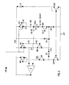
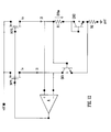
- FIG. 4 presents a first embodiment of a bandgap reference voltage circuit in accordance with the present invention.
- the circuit includes an amplifier A having an inverting and a non-inverting input and providing at its output a voltage reference, Vref. Coupled to the inputs of the amplifier are two PNP bipolar transistors, QP1, QP2, each having the same emitter area, two NPN bipolar transistors, QN1 and QN2, QN2 having an emitter area of n times that of QN1, and two resistors, R1 and R2.
- the first PNP transistor QP1 is provided in a feedback configuration between the output node of the amplifier and the inverting input.
- the base of QP1 is coupled to the base of the first NPN transistor QN1 and is also coupled to the inverting input.
- the collector of transistor QN1 is coupled to the collector of transistor QP1, and also to the non-inverting input of the amplifier.
- transistor QP2 is provided in a diode configuration with the base being directly coupled to the collector and also to the commonly coupled bases of QP1 and QN1, thereby connecting the first and second arms of the circuit.
- the emitter is coupled to the output node of the amplifier.
- Transistor QN2 is also provided in a diode configuration and the collector is coupled across resistor R1 to the base of QP2.
- the emitter of QN2 is coupled across resistor R2 to ground, and is directly coupled to the emitter of QN1. It will be appreciated that the components of Figure 4 , QN1, QN2, R1 and the amplifier, are all components of the PTAT cell of Figure 3 .
- the current mirror block of Figure 3 is provided by the two PNP transistors QP1 and QP2: QP2 being the master transistor and QP1 the slave.
- QN1 and QN2 each operate at a different collector current density and a PTAT voltage of the form of Eq. (1) is developed across R1. In the circuit of Figure 4 , this results in a corresponding PTAT current flowing from the reference voltage node "Vref" via QP2, R1, QN2, R2 to the ground, gnd. If QP1 is provided having the same emitter area as QP2, the current flowing from Vref to ground via QP1, QN1 and R2 is the same as the current flows from Vref node via QP2, R1, QN2, R2.
- the amplifier A biased with a current I1, operating in accordance with known amplifier characteristics is adapted to keep the base-collector voltage of both transistors, QP1 and QN1, close to zero and also to generate the reference voltage at node Vref. As a result all four transistors in the main cell, QP1, QP2, QN1, QN2, are operating at zero base-collector voltage thereby reducing the Early effect to zero.
- QP1 and QP2 have the same emitter area and because they have the same base-emitter voltage (both being coupled to Vref), their collector currents are the same.
- the collector current of QP1 also flows into the collector current of QN1.
- QP1, QP2 and QN1 have all the same collector current, lp.
- the collector current of QN2 is different due to the bias current of QP2 and the bias current difference of QP1 and QN1.
- These bias currents are related to what is commonly termed as a "beta" factor or ⁇ (ratio of the collector current to the bias current).
- ⁇ Vbe base-emitter voltage difference devebped across r1
- ⁇ ⁇ V be KT q ⁇ ln n ⁇ Ic Q ⁇ N 1
- Ic Q ⁇ N 2 KT q ⁇ ln n + KT q ⁇ ln Err
- the second term of (10) is an error factor which can be minimised by properly scaling the emitter areas of the four bipolar transistors, QP1, QP2, QN1 and QN2.
- the four transistors are specifically chosen to minimise the effect of this beta factor error, there is a certain minimum intrinsic error that will remain resulting from beta factor variation due to the temperature and process variation.
- beta factors are greater than 100 and their relative variation is of the order of +/-15%. If this is the case the worst beta variation of the bipolar transistors will be reflected as an voltage variation of less than 1 mV into a 2.5V reference.
- the present invention provides, in certain embodiments, for a compensation of this inherent voltage curvature. In order to do this it is necessary to provide a TlogT signal of opposite sign to the inherent TlogT signal generated.
- the present invention provides for the generation of this TlogT signal by providing a CTAT current 12, which may be externally generated from the circuit described thus far and using this current in combination with a third resistor, R3.
- the CTAT current 12 is mirrored via a diode configured transistor QN5 to another NPN transistor QN4 and the CTAT current reflected on the collector of QN4 is pulled from the reference node, Vref, via two bipolar transistors: QP3 of the same emitter area as QP1, and QN3 of the same emitter area as QN1.
- the resistor R3 is provided between the commonly coupled collector of QN4/emitter of QN3 and the emitter of QN1.
- a very important feature of the circuit described thus far is related to the very low influence of any amplifier errors on the reference voltage. This is because the base-collector voltages of QP1 and QN1 have very little effect on their respective base-emitter voltages and collector currents and as a result the reference voltage provided at the output of the amplifier is not greatly affected by the amplifier's errors. It will be understood that the pairing of QP1 and QN1 provide an pre-amplification of the signal prior to the amplification effect of the amplifier A. They act, in effect as the first stage of an amplifier, thereby reducing the error contribution of the actual amplifier. In other words, the amplifier controls a parameter which has a second order effect on the reference voltage but at the same time it forces the necessary reference voltage.
- the amplifier A can be formed as a simple amplifier having low gain by using for example MOS input components. The use of such components reduces the current taken by the amplifier to zero. As the total loop gain will be very high, the line regulation (or power supply rejection ratio (PSRR)) and load regulation will be very high as simulations shows.
- PSRR power supply rejection ratio
- the circuit of Figure 4 provides a bandgap voltage cell which will typically provide, using standard components, a reference voltage of the order of 2.3V.
- This voltage can be simply scaled to a standard voltage of 2.5V by modifying the circuit to insert a single resistor, R4, as shown in Figure 5 .
- One side of the resistor is coupled to the output of the amplifier and the other side is coupled to the common node between the emitter of QN1 and the emitter of QN2. Across this resistor, R4, a pure CTAT voltage is reflected generating a corresponding shifting CTAT current which flows into R2.
- the reference voltage may be provided with a flat response over the temperature range. As the supply current for the amplifier can be set very low and because there is no need for any resistor divider to set the reference voltage the resulting reference voltage will have very low supply current.
- FIG. 6 shows a further modification to the circuit of Figure 4 where a bipolar transistor, QP4, is provided in series between resistor R4 and the output of the amplifier.
- This transistor can generate and mirror a CTAT current, via another bipolar transistor QP5, so as to generate a bias voltage internally within the circuit thereby obviating the need for the externally generated current I2 present in Figures 4 and 5 .
- the amplifier in Figures 4 to 6 may be provided as a two stage MOS/bipolar amplifier and such components are explicitly detailed in Figure 7 .
- the amplifier has two inputs, a non-inverting, Inp, and an inverting input, Inn.
- An output, o is also provided.
- the input stage of the amplifier is based on two pMOS devices, mp1 and mp2 biased with a current I1.
- the loads into the first stage are qn1 and qn2.
- the second stage is an inverter, qn3, biased with a current I2.
- Transistor devices qn5 and qn6 form a Darlington pair in order to provide the required output current.
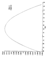
- FIG. 8 A simulation of the performance of the circuits of Figures 4 to 7 was conducted for an extended temperature range, from-55C to 125C and total supply current, and is shown in Figure 8 .
- the total voltage variation is about 20uV which corresponds to 0.05ppm.
- the total supply current is less than 41 uA.
- r5 r6 when generating a reference voltage at the amplifier's output of the order of 2.5V the voltage drop across r5 is about 1.25V.
- the only current flowing into the resistor divider, r5 r6, is of the order of 100uA, more than twice total supply current for the circuit according to Figure 4 to 7 .
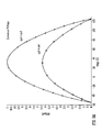
- Figure 9A presents the deviation tom the straight line (or curvature) of the base-emitter voltage of qp3 plus qn3, ( Figure 6 ) and the corresponding voltage deviation of qp1 plus qn2.
- Their difference, ⁇ V is shown in Figure 9B .
- This curvature difference of the order of 5mV at room temperature is reflected across r3 .
- a corresponding current will flow from r3 to r2 for exact cancellation of the curvature voltage of the base-emitter voltage of qp1 plus qn1.
- Simulations of the reference voltage assuming firstly no offset and secondly where a 5mV offset voltage is present at the input of the amplifier indicate that a 5mV offset voltage of the amplifier is reflected as 0.12mv into the reference voltage. This corresponds to a reduction of the offset input voltage by a factor of more than 40 as compared to a reduction of the order of 2 as may be achieved in a typical Brokaw cell.
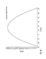
- FIG 10 presents the reference voltage supply rejection, or PSRR. This very high PSRR is due to high open loop gain primarily due to QP1 and QN1.
- the circuits of the present invention can provide a high open loop gain. This open loop gain can be increased more and the noise can also be reduced if QP1 and QP2 are each set to have a different current density, for example by making QP1 as a multiple emitter device and inserting a resistor from the reference voltage node to the emitter of QP1 as Figure 11 shows.
- the circuit of Figure 11 is substantially the same as the circuit of Figure 6 except that the emitter ratio of QP1 to QP2 is "n", the same as the corresponding ratio for QN2 and QN1 and a new resistor, R5 is inserted between the reference voltage and the emitter of QP1.
- the circuit according to Figure 11 was also simulated using typical value for the component devices and it was found that the PSRR achievable using this modified circuit is about 10db greater as compared to Figure 10 . It was also found that the total noise of the circuit according to Figure 11 is half that compared to Figure 10 and this is mainly because QP1 has larger emitter area and it also has a degeneration resistor.
- the two PNP transistors (OP1, QP2) that are provided on each of the arms of the circuit of Figures 4-6 and 11 effectively form the current mirror circuit 300 of Figure 3 which is used to drive the NPN transistors that are coupled to the inputs of the amplifier.
- Such a current mirror 300 which can be easily provided in either a bipolar (as shown in Figures 4-6 and 11 ) or MOS configuration, as shown in Figure 12 .
- the currents I1 and I2 which are provided to the transistors NP1 and NP2 may be provided by MOS devices MP1 and MP2 (in this example shown as P type devices) whose gates are coupled to the output of the amplifier and whose sources are coupled to Vdd.
- the circuit provides a bridge arrangement of transistors coupled to first and second inputs of the amplifier, with a first arm of the bridge including a transistor operating at a first current density and a second arm of the bridge operating at a second, higher, current density.
- a measure of the difference in base emitter voltages between the two transistors is provided by a resistor network coupled to the second arm.
- the first arm is coupled to an intermediate point on the resistor network and both arms are coupled via the current mirror to the output of the amplifier.
- each of the arms via the mirror to the output serves to drive the bases of each of the transistors with the same voltage and as their collectors are also at the same potential (each collector being coupled to a respective input of the amplifier) the circuit serves to reduce the base collector voltages of the transistors to a minimum value, thereby reducing the Early effect.
- the present invention provides a bandgap voltage reference circuit that utilises an amplifier with an inverting and non-inverting input and providing at its output a voltage reference.
- First and second arms of circuitry are provided, each arm being coupled to a defined input of the amplifier.
- NPN and PNP bipolar transistor in a first arm and coupling the bases of these two transistors together it is possible to connect the two arms of the amplifier.
- This provides a plurality of advantages including the possibility of these transistors providing amplification functionality equivalent to a first stage of an amplifier.
- By providing a "second" amplifier it is possible to reduce the complexity of the architecture of the actual amplifier and also to reduce the errors introduced at the inputs of the amplifier.
Claims (8)
- Circuit de tension incluant un premier amplificateur (A) ayant des première et seconde entrées et ayant une sortie commandant un circuit à miroir de courant, des sorties du circuit à miroir de courant commandant des premier (QN1) et second (QN2) transistors bipolaires de type N qui sont couplés respectivement aux première et seconde entrées de l'amplificateur, la base du premier transistor bipolaire de type N étant couplée à la seconde entrée de l'amplificateur et le collecteur du premier transistor bipolaire de type N étant couplé à la première entrée de l'amplificateur de sorte que l'amplificateur maintient la base et le collecteur du premier transistor bipolaire de type N au même potentiel, le second transistor bipolaire de type N étant agencé dans une configuration de diode, et dans lequel les premier et second transistors bipolaires de type N sont adaptés pour fonctionner à différentes densités de courant de sorte qu'une différence de tensions base-émetteur entre les premier et second transistors bipolaires de type N est générée à travers une charge résistive (R1) couplée au second transistor bipolaire de type N, la différence de tensions base-émetteur étant une tension proportionnelle à la tension de température absolue (PTAT), caractérisé en ce que : le circuit à miroir de courant inclut des premier (QP1) et second (QP2) transistors bipolaires de type P, le second transistor bipolaire de type P étant agencé dans une configuration de diode avec la base et le collecteur couplés en commun au second transistor bipolaire de type N via la charge résistive, la base du premier transistor bipolaire de type P étant couplée à la base du premier transistor bipolaire de type N et également à la seconde entrée de l'amplificateur, le collecteur du premier transistor bipolaire de type P étant couplé au collecteur du premier transistor bipolaire de type N et également à la première entrée de l'amplificateur, l'agencement du premier transistor bipolaire de type P et du premier transistor bipolaire de type N assurant une pré-amplification du signal avant l'amplification assurée par l'amplificateur.
- Circuit tel que revendiqué dans la revendication 1, dans lequel le premier transistor bipolaire de type P et le premier transistor bipolaire de type N forment un premier étage d'un amplificateur.
- Circuit tel que revendiqué dans la revendication 1, dans lequel les émetteurs des premier et second transistors bipolaires de type N sont tous deux couplés à la masse via une deuxième charge résistive.
- Circuit tel que revendiqué dans la revendication 3, incluant en outre des circuits supplémentaires adaptés pour assurer une correction de courbure, les circuits supplémentaires incluant une source de courant complémentaire à la température absolue (CTAT) et une troisième charge résistive, la troisième charge résistive étant couplée aux émetteurs des premier et second transistors bipolaires de type N et une mise à l'échelle de la valeur des deuxième et troisième charges résistives étant utilisée pour corriger la courbure.
- Circuit tel que revendiqué dans la revendication 4, dans lequel le courant CTAT est utilisé en miroir par un second ensemble de circuits à miroir de courant, le second ensemble de circuits à miroir de courant incluant un transistor maître et un transistor esclave et dans lequel le transistor esclave est couplé à la sortie de l'amplificateur par deux transistors connectés en diode, la troisième charge résistive étant couplée au transistor esclave, de sorte qu'un courant CTAT réfléchi sur le collecteur du transistor esclave est prélevé de la sortie de l'amplificateur de manière à générer un signal du type de TlogT à travers la troisième charge résistive.
- Circuit tel que revendiqué dans la revendication 5, dans lequel la source de courant CTAT est fournie extérieurement au circuit.
- Circuit tel que revendiqué dans la revendication 5, incluant en outre une quatrième charge résistive, la quatrième charge résistive étant agencée entre la sortie de l'amplificateur et les émetteurs couplés en commun des premier et second transistors bipolaires de type N, la fourniture de la quatrième charge résistive permettant une mise à l'échelle de la tension délivrée à la sortie de l'amplificateur.
- Circuit tel que revendiqué dans la revendication 1, dans lequel les aires d'émetteur des premier et second transistors bipolaires de type P sont différentes, de telle sorte que les premier et second transistors de type P fonctionnent à différentes densités de courant en augmentant ainsi le gain en boucle ouverte du circuit.
Applications Claiming Priority (2)
| Application Number | Priority Date | Filing Date | Title |
|---|---|---|---|
| US10/881,300 US7173407B2 (en) | 2004-06-30 | 2004-06-30 | Proportional to absolute temperature voltage circuit |
| PCT/EP2005/052737 WO2006003083A1 (fr) | 2004-06-30 | 2005-06-14 | Circuit de tension proportionnel a la temperature absolue |
Publications (2)
| Publication Number | Publication Date |
|---|---|
| EP1769301A1 EP1769301A1 (fr) | 2007-04-04 |
| EP1769301B1 true EP1769301B1 (fr) | 2011-11-16 |
Family
ID=34970849
Family Applications (1)
| Application Number | Title | Priority Date | Filing Date |
|---|---|---|---|
| EP05754213A Not-in-force EP1769301B1 (fr) | 2004-06-30 | 2005-06-14 | Circuit de tension proportionnel a la temperature absolue |
Country Status (7)
| Country | Link |
|---|---|
| US (1) | US7173407B2 (fr) |
| EP (1) | EP1769301B1 (fr) |
| JP (1) | JP4809340B2 (fr) |
| CN (1) | CN100511083C (fr) |
| AT (1) | ATE534066T1 (fr) |
| TW (1) | TWI282050B (fr) |
| WO (1) | WO2006003083A1 (fr) |
Families Citing this family (59)
| Publication number | Priority date | Publication date | Assignee | Title |
|---|---|---|---|---|
| US7543253B2 (en) * | 2003-10-07 | 2009-06-02 | Analog Devices, Inc. | Method and apparatus for compensating for temperature drift in semiconductor processes and circuitry |
| US7256643B2 (en) * | 2005-08-04 | 2007-08-14 | Micron Technology, Inc. | Device and method for generating a low-voltage reference |
| US7411380B2 (en) * | 2006-07-21 | 2008-08-12 | Faraday Technology Corp. | Non-linearity compensation circuit and bandgap reference circuit using the same |
| US8102201B2 (en) | 2006-09-25 | 2012-01-24 | Analog Devices, Inc. | Reference circuit and method for providing a reference |
| US7576598B2 (en) * | 2006-09-25 | 2009-08-18 | Analog Devices, Inc. | Bandgap voltage reference and method for providing same |
| JP2008123480A (ja) * | 2006-10-16 | 2008-05-29 | Nec Electronics Corp | 基準電圧発生回路 |
| US7486129B2 (en) * | 2007-03-01 | 2009-02-03 | Freescale Semiconductor, Inc. | Low power voltage reference |
| US7714563B2 (en) * | 2007-03-13 | 2010-05-11 | Analog Devices, Inc. | Low noise voltage reference circuit |
| US20080265860A1 (en) * | 2007-04-30 | 2008-10-30 | Analog Devices, Inc. | Low voltage bandgap reference source |
| US7773446B2 (en) * | 2007-06-29 | 2010-08-10 | Sandisk 3D Llc | Methods and apparatus for extending the effective thermal operating range of a memory |
| US7656734B2 (en) * | 2007-06-29 | 2010-02-02 | Sandisk 3D Llc | Methods and apparatus for extending the effective thermal operating range of a memory |
| US20090027030A1 (en) * | 2007-07-23 | 2009-01-29 | Analog Devices, Inc. | Low noise bandgap voltage reference |
| US7605578B2 (en) * | 2007-07-23 | 2009-10-20 | Analog Devices, Inc. | Low noise bandgap voltage reference |
| US7612606B2 (en) * | 2007-12-21 | 2009-11-03 | Analog Devices, Inc. | Low voltage current and voltage generator |
| US7598799B2 (en) * | 2007-12-21 | 2009-10-06 | Analog Devices, Inc. | Bandgap voltage reference circuit |
| CN101226414B (zh) * | 2008-01-30 | 2012-01-11 | 北京中星微电子有限公司 | 一种动态补偿基准电压的方法以及带隙基准电压源 |
| US7880533B2 (en) * | 2008-03-25 | 2011-02-01 | Analog Devices, Inc. | Bandgap voltage reference circuit |
| US7750728B2 (en) * | 2008-03-25 | 2010-07-06 | Analog Devices, Inc. | Reference voltage circuit |
| US7902912B2 (en) * | 2008-03-25 | 2011-03-08 | Analog Devices, Inc. | Bias current generator |
| US8710912B2 (en) * | 2008-11-24 | 2014-04-29 | Analog Device, Inc. | Second order correction circuit and method for bandgap voltage reference |
| EP2356533B1 (fr) * | 2008-11-25 | 2016-06-29 | Linear Technology Corporation | Circuit, reim et agencement pour compensation en température de résistances métalliques dans des puces à semi-conducteur |
| US9004754B2 (en) * | 2009-04-22 | 2015-04-14 | Taiwan Semiconductor Manufacturing Company, Ltd. | Thermal sensors and methods of operating thereof |
| US8475039B2 (en) | 2009-04-22 | 2013-07-02 | Taiwan Semiconductor Manufacturing Company, Ltd. | Providing linear relationship between temperature and digital code |
| US8207724B2 (en) * | 2009-09-16 | 2012-06-26 | Mediatek Singapore Pte. Ltd. | Bandgap voltage reference with dynamic element matching |
| US8330445B2 (en) * | 2009-10-08 | 2012-12-11 | Intersil Americas Inc. | Circuits and methods to produce a VPTAT and/or a bandgap voltage with low-glitch preconditioning |
| US8536854B2 (en) * | 2010-09-30 | 2013-09-17 | Cirrus Logic, Inc. | Supply invariant bandgap reference system |
| US8378735B2 (en) * | 2010-11-29 | 2013-02-19 | Freescale Semiconductor, Inc. | Die temperature sensor circuit |
| US9442508B2 (en) * | 2012-03-05 | 2016-09-13 | Freescale Semiconductor, Inc. | Reference voltage source and method for providing a curvature-compensated reference voltage |
| US9448579B2 (en) * | 2013-12-20 | 2016-09-20 | Analog Devices Global | Low drift voltage reference |
| US9658637B2 (en) * | 2014-02-18 | 2017-05-23 | Analog Devices Global | Low power proportional to absolute temperature current and voltage generator |
| US10367514B2 (en) | 2015-01-24 | 2019-07-30 | Circuit Seed, Llc | Passive phased injection locked circuit |
| TWI564692B (zh) * | 2015-03-11 | 2017-01-01 | 晶豪科技股份有限公司 | 能隙參考電路 |
| US10345346B2 (en) * | 2015-07-12 | 2019-07-09 | Skyworks Solutions, Inc. | Radio-frequency voltage detection |
| CA3031736A1 (fr) | 2015-07-29 | 2017-02-02 | Circuit Seed, Llc | Dispositifs a transistor a effet de champ a courant complementaire et amplificateurs |
| US10491177B2 (en) | 2015-07-30 | 2019-11-26 | Circuit Seed, Llc | Multi-stage and feed forward compensated complementary current field effect transistor amplifiers |
| CN108141180A (zh) | 2015-07-30 | 2018-06-08 | 电路种子有限责任公司 | 基于互补电流场效应晶体管装置的低噪声跨阻抗放大器 |
| US10514716B2 (en) | 2015-07-30 | 2019-12-24 | Circuit Seed, Llc | Reference generator and current source transistor based on complementary current field-effect transistor devices |
| CN105204564A (zh) * | 2015-10-30 | 2015-12-30 | 无锡纳讯微电子有限公司 | 一种低温度系数基准源电路 |
| CN108140613B (zh) | 2015-12-14 | 2020-07-28 | 电路种子有限责任公司 | 过饱和电流场效应晶体管和跨阻抗mos装置 |
| US10078016B2 (en) * | 2016-02-10 | 2018-09-18 | Nxp Usa, Inc. | On-die temperature sensor for integrated circuit |
| JP6685168B2 (ja) * | 2016-04-15 | 2020-04-22 | 新日本無線株式会社 | 基準電圧回路 |
| CN105955384B (zh) * | 2016-07-19 | 2018-02-23 | 南方科技大学 | 一种非带隙基准电压源 |
| US10222817B1 (en) | 2017-09-29 | 2019-03-05 | Cavium, Llc | Method and circuit for low voltage current-mode bandgap |
| US9864389B1 (en) * | 2016-11-10 | 2018-01-09 | Analog Devices Global | Temperature compensated reference voltage circuit |
| CN106411127A (zh) * | 2016-11-22 | 2017-02-15 | 郑州搜趣信息技术有限公司 | 一种pwm调制转换电路 |
| CN109002075B (zh) * | 2017-06-07 | 2021-07-23 | 苏州瀚宸科技有限公司 | 双极型晶体管的基极电流镜像电路、rssi电路及芯片 |
| US10557894B2 (en) * | 2017-08-07 | 2020-02-11 | Linear Technology Holding Llc | Reference signal correction circuit |
| US10691156B2 (en) * | 2017-08-31 | 2020-06-23 | Texas Instruments Incorporated | Complementary to absolute temperature (CTAT) voltage generator |
| IT201700117023A1 (it) * | 2017-10-17 | 2019-04-17 | St Microelectronics Srl | Circuito di riferimento bandgap, dispositivo e procedimento corrispondenti |
| CN108614611A (zh) * | 2018-06-27 | 2018-10-02 | 上海治精微电子有限公司 | 低噪声带隙基准电压源、电子设备 |
| US10409312B1 (en) * | 2018-07-19 | 2019-09-10 | Analog Devices Global Unlimited Company | Low power duty-cycled reference |
| US10691155B2 (en) * | 2018-09-12 | 2020-06-23 | Infineon Technologies Ag | System and method for a proportional to absolute temperature circuit |
| US10794761B2 (en) * | 2018-11-09 | 2020-10-06 | Linear Technology Holding Llc | Logarithmic scale analog to digital converter for wide dynamic range avalanche photodiode current companding |
| US11068011B2 (en) * | 2019-10-30 | 2021-07-20 | Taiwan Semiconductor Manufacturing Company Ltd. | Signal generating device and method of generating temperature-dependent signal |
| JP2022072600A (ja) * | 2020-10-30 | 2022-05-17 | エイブリック株式会社 | 基準電圧回路 |
| CN112256078B (zh) * | 2020-10-30 | 2021-12-31 | 电子科技大学 | 一种正温系数电流源和一种零温度系数电流源 |
| JP2022139688A (ja) * | 2021-03-12 | 2022-09-26 | 株式会社東芝 | バンドギャップ型基準電圧発生回路 |
| US11429125B1 (en) | 2021-03-18 | 2022-08-30 | Texas Instruments Incorporated | Mitigation of voltage shift induced by mechanical stress in bandgap voltage reference circuits |
| CN115328258A (zh) * | 2022-09-22 | 2022-11-11 | 武汉泽声微电子有限公司 | 带隙基准电路 |
Citations (1)
| Publication number | Priority date | Publication date | Assignee | Title |
|---|---|---|---|---|
| EP0714055A1 (fr) * | 1994-11-18 | 1996-05-29 | AT&T Corp. | Source de courant proportionnel à la température absolue |
Family Cites Families (15)
| Publication number | Priority date | Publication date | Assignee | Title |
|---|---|---|---|---|
| US4399398A (en) | 1981-06-30 | 1983-08-16 | Rca Corporation | Voltage reference circuit with feedback circuit |
| JP2695515B2 (ja) * | 1990-07-19 | 1997-12-24 | ローム株式会社 | 基準電圧発生回路 |
| US5352973A (en) * | 1993-01-13 | 1994-10-04 | Analog Devices, Inc. | Temperature compensation bandgap voltage reference and method |
| JPH09330137A (ja) * | 1996-04-10 | 1997-12-22 | Toshiba Corp | 基準電圧発生回路及び基準電圧発生方法 |
| US5796244A (en) * | 1997-07-11 | 1998-08-18 | Vanguard International Semiconductor Corporation | Bandgap reference circuit |
| US6531857B2 (en) * | 2000-11-09 | 2003-03-11 | Agere Systems, Inc. | Low voltage bandgap reference circuit |
| TW574782B (en) * | 2002-04-30 | 2004-02-01 | Realtek Semiconductor Corp | Fast start-up low-voltage bandgap voltage reference circuit |
| US6737849B2 (en) | 2002-06-19 | 2004-05-18 | International Business Machines Corporation | Constant current source having a controlled temperature coefficient |
| FR2842317B1 (fr) * | 2002-07-09 | 2004-10-01 | Atmel Nantes Sa | Source de tension de reference, capteur de temperature, detecteur de seuil de temperature, puce et systeme correspondant |
| US6664847B1 (en) | 2002-10-10 | 2003-12-16 | Texas Instruments Incorporated | CTAT generator using parasitic PNP device in deep sub-micron CMOS process |
| US6690228B1 (en) | 2002-12-11 | 2004-02-10 | Texas Instruments Incorporated | Bandgap voltage reference insensitive to voltage offset |
| US6885178B2 (en) * | 2002-12-27 | 2005-04-26 | Analog Devices, Inc. | CMOS voltage bandgap reference with improved headroom |
| US6815941B2 (en) * | 2003-02-05 | 2004-11-09 | United Memories, Inc. | Bandgap reference circuit |
| US7012416B2 (en) * | 2003-12-09 | 2006-03-14 | Analog Devices, Inc. | Bandgap voltage reference |
| US7211993B2 (en) * | 2004-01-13 | 2007-05-01 | Analog Devices, Inc. | Low offset bandgap voltage reference |
-
2004
- 2004-06-30 US US10/881,300 patent/US7173407B2/en active Active
-
2005
- 2005-05-27 TW TW094117525A patent/TWI282050B/zh not_active IP Right Cessation
- 2005-06-14 WO PCT/EP2005/052737 patent/WO2006003083A1/fr active Application Filing
- 2005-06-14 EP EP05754213A patent/EP1769301B1/fr not_active Not-in-force
- 2005-06-14 CN CNB2005800218621A patent/CN100511083C/zh not_active Expired - Fee Related
- 2005-06-14 JP JP2007519760A patent/JP4809340B2/ja not_active Expired - Fee Related
- 2005-06-14 AT AT05754213T patent/ATE534066T1/de active
Patent Citations (1)
| Publication number | Priority date | Publication date | Assignee | Title |
|---|---|---|---|---|
| EP0714055A1 (fr) * | 1994-11-18 | 1996-05-29 | AT&T Corp. | Source de courant proportionnel à la température absolue |
Also Published As
| Publication number | Publication date |
|---|---|
| US20060001413A1 (en) | 2006-01-05 |
| TWI282050B (en) | 2007-06-01 |
| JP4809340B2 (ja) | 2011-11-09 |
| JP2008505412A (ja) | 2008-02-21 |
| CN100511083C (zh) | 2009-07-08 |
| EP1769301A1 (fr) | 2007-04-04 |
| CN1977225A (zh) | 2007-06-06 |
| US7173407B2 (en) | 2007-02-06 |
| WO2006003083A1 (fr) | 2006-01-12 |
| ATE534066T1 (de) | 2011-12-15 |
| TW200609704A (en) | 2006-03-16 |
Similar Documents
| Publication | Publication Date | Title |
|---|---|---|
| EP1769301B1 (fr) | Circuit de tension proportionnel a la temperature absolue | |
| US7012416B2 (en) | Bandgap voltage reference | |
| JP4817825B2 (ja) | 基準電圧発生回路 | |
| JP3039454B2 (ja) | 基準電圧発生回路 | |
| JP4616281B2 (ja) | 低オフセット・バンドギャップ電圧基準 | |
| US6885178B2 (en) | CMOS voltage bandgap reference with improved headroom | |
| US20070176591A1 (en) | Voltage reference circuit compensated for non-linearity in temperature characteristic of diode | |
| US7053694B2 (en) | Band-gap circuit with high power supply rejection ratio | |
| US7612606B2 (en) | Low voltage current and voltage generator | |
| US8102201B2 (en) | Reference circuit and method for providing a reference | |
| US20080265860A1 (en) | Low voltage bandgap reference source | |
| US20150338872A1 (en) | Curvature-corrected bandgap reference | |
| US6680643B2 (en) | Bandgap type reference voltage source with low supply voltage | |
| US8085029B2 (en) | Bandgap voltage and current reference | |
| US6509783B2 (en) | Generation of a voltage proportional to temperature with a negative variation | |
| US6509782B2 (en) | Generation of a voltage proportional to temperature with stable line voltage | |
| EP3926437B1 (fr) | Circuit de référence de tension zener de haute précision | |
| US6433529B1 (en) | Generation of a voltage proportional to temperature with accurate gain control | |
| KR100599974B1 (ko) | 기준 전압 발생기 | |
| CN217640051U (zh) | 带隙基准电路 | |
| JP2022159875A (ja) | 定電流回路 | |
| CN116643615A (zh) | 具有微调电路的带隙参考电路 | |
| CN116909348A (zh) | 曲率补偿电路及包括其的带隙基准电压源 |
Legal Events
| Date | Code | Title | Description |
|---|---|---|---|
| PUAI | Public reference made under article 153(3) epc to a published international application that has entered the european phase |
Free format text: ORIGINAL CODE: 0009012 |
|
| 17P | Request for examination filed |
Effective date: 20070119 |
|
| AK | Designated contracting states |
Kind code of ref document: A1 Designated state(s): AT BE BG CH CY CZ DE DK EE ES FI FR GB GR HU IE IS IT LI LT LU MC NL PL PT RO SE SI SK TR |
|
| DAX | Request for extension of the european patent (deleted) | ||
| 17Q | First examination report despatched |
Effective date: 20090121 |
|
| GRAP | Despatch of communication of intention to grant a patent |
Free format text: ORIGINAL CODE: EPIDOSNIGR1 |
|
| GRAS | Grant fee paid |
Free format text: ORIGINAL CODE: EPIDOSNIGR3 |
|
| GRAA | (expected) grant |
Free format text: ORIGINAL CODE: 0009210 |
|
| AK | Designated contracting states |
Kind code of ref document: B1 Designated state(s): AT BE BG CH CY CZ DE DK EE ES FI FR GB GR HU IE IS IT LI LT LU MC NL PL PT RO SE SI SK TR |
|
| REG | Reference to a national code |
Ref country code: GB Ref legal event code: FG4D |
|
| REG | Reference to a national code |
Ref country code: CH Ref legal event code: EP |
|
| REG | Reference to a national code |
Ref country code: IE Ref legal event code: FG4D |
|
| REG | Reference to a national code |
Ref country code: DE Ref legal event code: R096 Ref document number: 602005031241 Country of ref document: DE Effective date: 20120112 |
|
| REG | Reference to a national code |
Ref country code: NL Ref legal event code: VDEP Effective date: 20111116 |
|
| LTIE | Lt: invalidation of european patent or patent extension |
Effective date: 20111116 |
|
| PG25 | Lapsed in a contracting state [announced via postgrant information from national office to epo] |
Ref country code: IS Free format text: LAPSE BECAUSE OF FAILURE TO SUBMIT A TRANSLATION OF THE DESCRIPTION OR TO PAY THE FEE WITHIN THE PRESCRIBED TIME-LIMIT Effective date: 20120316 Ref country code: LT Free format text: LAPSE BECAUSE OF FAILURE TO SUBMIT A TRANSLATION OF THE DESCRIPTION OR TO PAY THE FEE WITHIN THE PRESCRIBED TIME-LIMIT Effective date: 20111116 |
|
| PG25 | Lapsed in a contracting state [announced via postgrant information from national office to epo] |
Ref country code: SE Free format text: LAPSE BECAUSE OF FAILURE TO SUBMIT A TRANSLATION OF THE DESCRIPTION OR TO PAY THE FEE WITHIN THE PRESCRIBED TIME-LIMIT Effective date: 20111116 Ref country code: PT Free format text: LAPSE BECAUSE OF FAILURE TO SUBMIT A TRANSLATION OF THE DESCRIPTION OR TO PAY THE FEE WITHIN THE PRESCRIBED TIME-LIMIT Effective date: 20120316 Ref country code: BE Free format text: LAPSE BECAUSE OF FAILURE TO SUBMIT A TRANSLATION OF THE DESCRIPTION OR TO PAY THE FEE WITHIN THE PRESCRIBED TIME-LIMIT Effective date: 20111116 Ref country code: SI Free format text: LAPSE BECAUSE OF FAILURE TO SUBMIT A TRANSLATION OF THE DESCRIPTION OR TO PAY THE FEE WITHIN THE PRESCRIBED TIME-LIMIT Effective date: 20111116 Ref country code: GR Free format text: LAPSE BECAUSE OF FAILURE TO SUBMIT A TRANSLATION OF THE DESCRIPTION OR TO PAY THE FEE WITHIN THE PRESCRIBED TIME-LIMIT Effective date: 20120217 Ref country code: NL Free format text: LAPSE BECAUSE OF FAILURE TO SUBMIT A TRANSLATION OF THE DESCRIPTION OR TO PAY THE FEE WITHIN THE PRESCRIBED TIME-LIMIT Effective date: 20111116 Ref country code: PL Free format text: LAPSE BECAUSE OF FAILURE TO SUBMIT A TRANSLATION OF THE DESCRIPTION OR TO PAY THE FEE WITHIN THE PRESCRIBED TIME-LIMIT Effective date: 20111116 |
|
| PG25 | Lapsed in a contracting state [announced via postgrant information from national office to epo] |
Ref country code: CY Free format text: LAPSE BECAUSE OF FAILURE TO SUBMIT A TRANSLATION OF THE DESCRIPTION OR TO PAY THE FEE WITHIN THE PRESCRIBED TIME-LIMIT Effective date: 20111116 |
|
| PG25 | Lapsed in a contracting state [announced via postgrant information from national office to epo] |
Ref country code: DK Free format text: LAPSE BECAUSE OF FAILURE TO SUBMIT A TRANSLATION OF THE DESCRIPTION OR TO PAY THE FEE WITHIN THE PRESCRIBED TIME-LIMIT Effective date: 20111116 Ref country code: SK Free format text: LAPSE BECAUSE OF FAILURE TO SUBMIT A TRANSLATION OF THE DESCRIPTION OR TO PAY THE FEE WITHIN THE PRESCRIBED TIME-LIMIT Effective date: 20111116 Ref country code: EE Free format text: LAPSE BECAUSE OF FAILURE TO SUBMIT A TRANSLATION OF THE DESCRIPTION OR TO PAY THE FEE WITHIN THE PRESCRIBED TIME-LIMIT Effective date: 20111116 Ref country code: CZ Free format text: LAPSE BECAUSE OF FAILURE TO SUBMIT A TRANSLATION OF THE DESCRIPTION OR TO PAY THE FEE WITHIN THE PRESCRIBED TIME-LIMIT Effective date: 20111116 Ref country code: BG Free format text: LAPSE BECAUSE OF FAILURE TO SUBMIT A TRANSLATION OF THE DESCRIPTION OR TO PAY THE FEE WITHIN THE PRESCRIBED TIME-LIMIT Effective date: 20120216 |
|
| PG25 | Lapsed in a contracting state [announced via postgrant information from national office to epo] |
Ref country code: IT Free format text: LAPSE BECAUSE OF FAILURE TO SUBMIT A TRANSLATION OF THE DESCRIPTION OR TO PAY THE FEE WITHIN THE PRESCRIBED TIME-LIMIT Effective date: 20111116 Ref country code: RO Free format text: LAPSE BECAUSE OF FAILURE TO SUBMIT A TRANSLATION OF THE DESCRIPTION OR TO PAY THE FEE WITHIN THE PRESCRIBED TIME-LIMIT Effective date: 20111116 |
|
| REG | Reference to a national code |
Ref country code: AT Ref legal event code: MK05 Ref document number: 534066 Country of ref document: AT Kind code of ref document: T Effective date: 20111116 |
|
| PLBE | No opposition filed within time limit |
Free format text: ORIGINAL CODE: 0009261 |
|
| STAA | Information on the status of an ep patent application or granted ep patent |
Free format text: STATUS: NO OPPOSITION FILED WITHIN TIME LIMIT |
|
| 26N | No opposition filed |
Effective date: 20120817 |
|
| REG | Reference to a national code |
Ref country code: DE Ref legal event code: R097 Ref document number: 602005031241 Country of ref document: DE Effective date: 20120817 |
|
| PG25 | Lapsed in a contracting state [announced via postgrant information from national office to epo] |
Ref country code: MC Free format text: LAPSE BECAUSE OF NON-PAYMENT OF DUE FEES Effective date: 20120630 Ref country code: AT Free format text: LAPSE BECAUSE OF FAILURE TO SUBMIT A TRANSLATION OF THE DESCRIPTION OR TO PAY THE FEE WITHIN THE PRESCRIBED TIME-LIMIT Effective date: 20111116 |
|
| REG | Reference to a national code |
Ref country code: CH Ref legal event code: PL |
|
| REG | Reference to a national code |
Ref country code: CH Ref legal event code: PL |
|
| REG | Reference to a national code |
Ref country code: IE Ref legal event code: MM4A |
|
| PG25 | Lapsed in a contracting state [announced via postgrant information from national office to epo] |
Ref country code: CH Free format text: LAPSE BECAUSE OF NON-PAYMENT OF DUE FEES Effective date: 20120630 Ref country code: LI Free format text: LAPSE BECAUSE OF NON-PAYMENT OF DUE FEES Effective date: 20120630 Ref country code: IE Free format text: LAPSE BECAUSE OF NON-PAYMENT OF DUE FEES Effective date: 20120614 |
|
| PG25 | Lapsed in a contracting state [announced via postgrant information from national office to epo] |
Ref country code: FI Free format text: LAPSE BECAUSE OF FAILURE TO SUBMIT A TRANSLATION OF THE DESCRIPTION OR TO PAY THE FEE WITHIN THE PRESCRIBED TIME-LIMIT Effective date: 20111116 |
|
| PG25 | Lapsed in a contracting state [announced via postgrant information from national office to epo] |
Ref country code: ES Free format text: LAPSE BECAUSE OF FAILURE TO SUBMIT A TRANSLATION OF THE DESCRIPTION OR TO PAY THE FEE WITHIN THE PRESCRIBED TIME-LIMIT Effective date: 20120227 |
|
| PG25 | Lapsed in a contracting state [announced via postgrant information from national office to epo] |
Ref country code: TR Free format text: LAPSE BECAUSE OF FAILURE TO SUBMIT A TRANSLATION OF THE DESCRIPTION OR TO PAY THE FEE WITHIN THE PRESCRIBED TIME-LIMIT Effective date: 20111116 |
|
| PG25 | Lapsed in a contracting state [announced via postgrant information from national office to epo] |
Ref country code: LU Free format text: LAPSE BECAUSE OF NON-PAYMENT OF DUE FEES Effective date: 20120614 |
|
| PG25 | Lapsed in a contracting state [announced via postgrant information from national office to epo] |
Ref country code: HU Free format text: LAPSE BECAUSE OF FAILURE TO SUBMIT A TRANSLATION OF THE DESCRIPTION OR TO PAY THE FEE WITHIN THE PRESCRIBED TIME-LIMIT Effective date: 20050614 |
|
| REG | Reference to a national code |
Ref country code: FR Ref legal event code: PLFP Year of fee payment: 12 |
|
| REG | Reference to a national code |
Ref country code: FR Ref legal event code: PLFP Year of fee payment: 13 |
|
| REG | Reference to a national code |
Ref country code: FR Ref legal event code: PLFP Year of fee payment: 14 |
|
| PGFP | Annual fee paid to national office [announced via postgrant information from national office to epo] |
Ref country code: FR Payment date: 20210519 Year of fee payment: 17 Ref country code: DE Payment date: 20210519 Year of fee payment: 17 |
|
| PGFP | Annual fee paid to national office [announced via postgrant information from national office to epo] |
Ref country code: GB Payment date: 20210519 Year of fee payment: 17 |
|
| REG | Reference to a national code |
Ref country code: DE Ref legal event code: R119 Ref document number: 602005031241 Country of ref document: DE |
|
| GBPC | Gb: european patent ceased through non-payment of renewal fee |
Effective date: 20220614 |
|
| PG25 | Lapsed in a contracting state [announced via postgrant information from national office to epo] |
Ref country code: FR Free format text: LAPSE BECAUSE OF NON-PAYMENT OF DUE FEES Effective date: 20220630 |
|
| PG25 | Lapsed in a contracting state [announced via postgrant information from national office to epo] |
Ref country code: GB Free format text: LAPSE BECAUSE OF NON-PAYMENT OF DUE FEES Effective date: 20220614 Ref country code: DE Free format text: LAPSE BECAUSE OF NON-PAYMENT OF DUE FEES Effective date: 20230103 |