EP1768257B1 - High voltage high side transistor driver - Google Patents
High voltage high side transistor driver Download PDFInfo
- Publication number
- EP1768257B1 EP1768257B1 EP06016937.2A EP06016937A EP1768257B1 EP 1768257 B1 EP1768257 B1 EP 1768257B1 EP 06016937 A EP06016937 A EP 06016937A EP 1768257 B1 EP1768257 B1 EP 1768257B1
- Authority
- EP
- European Patent Office
- Prior art keywords
- side transistor
- signal
- high side
- module
- power input
- Prior art date
- Legal status (The legal status is an assumption and is not a legal conclusion. Google has not performed a legal analysis and makes no representation as to the accuracy of the status listed.)
- Not-in-force
Links
Images


Classifications
-
- H—ELECTRICITY
- H03—ELECTRONIC CIRCUITRY
- H03K—PULSE TECHNIQUE
- H03K17/00—Electronic switching or gating, i.e. not by contact-making and –breaking
- H03K17/51—Electronic switching or gating, i.e. not by contact-making and –breaking characterised by the components used
- H03K17/56—Electronic switching or gating, i.e. not by contact-making and –breaking characterised by the components used by the use, as active elements, of semiconductor devices
- H03K17/687—Electronic switching or gating, i.e. not by contact-making and –breaking characterised by the components used by the use, as active elements, of semiconductor devices the devices being field-effect transistors
- H03K17/689—Electronic switching or gating, i.e. not by contact-making and –breaking characterised by the components used by the use, as active elements, of semiconductor devices the devices being field-effect transistors with galvanic isolation between the control circuit and the output circuit
- H03K17/691—Electronic switching or gating, i.e. not by contact-making and –breaking characterised by the components used by the use, as active elements, of semiconductor devices the devices being field-effect transistors with galvanic isolation between the control circuit and the output circuit using transformer coupling
-
- H—ELECTRICITY
- H03—ELECTRONIC CIRCUITRY
- H03K—PULSE TECHNIQUE
- H03K17/00—Electronic switching or gating, i.e. not by contact-making and –breaking
- H03K17/18—Modifications for indicating state of switch
-
- H—ELECTRICITY
- H03—ELECTRONIC CIRCUITRY
- H03K—PULSE TECHNIQUE
- H03K17/00—Electronic switching or gating, i.e. not by contact-making and –breaking
- H03K17/51—Electronic switching or gating, i.e. not by contact-making and –breaking characterised by the components used
- H03K17/56—Electronic switching or gating, i.e. not by contact-making and –breaking characterised by the components used by the use, as active elements, of semiconductor devices
- H03K17/687—Electronic switching or gating, i.e. not by contact-making and –breaking characterised by the components used by the use, as active elements, of semiconductor devices the devices being field-effect transistors
- H03K17/6877—Electronic switching or gating, i.e. not by contact-making and –breaking characterised by the components used by the use, as active elements, of semiconductor devices the devices being field-effect transistors the control circuit comprising active elements different from those used in the output circuit
-
- H—ELECTRICITY
- H05—ELECTRIC TECHNIQUES NOT OTHERWISE PROVIDED FOR
- H05B—ELECTRIC HEATING; ELECTRIC LIGHT SOURCES NOT OTHERWISE PROVIDED FOR; CIRCUIT ARRANGEMENTS FOR ELECTRIC LIGHT SOURCES, IN GENERAL
- H05B41/00—Circuit arrangements or apparatus for igniting or operating discharge lamps
- H05B41/14—Circuit arrangements
- H05B41/26—Circuit arrangements in which the lamp is fed by power derived from DC by means of a converter, e.g. by high-voltage DC
- H05B41/28—Circuit arrangements in which the lamp is fed by power derived from DC by means of a converter, e.g. by high-voltage DC using static converters
- H05B41/282—Circuit arrangements in which the lamp is fed by power derived from DC by means of a converter, e.g. by high-voltage DC using static converters with semiconductor devices
- H05B41/2825—Circuit arrangements in which the lamp is fed by power derived from DC by means of a converter, e.g. by high-voltage DC using static converters with semiconductor devices by means of a bridge converter in the final stage
-
- H—ELECTRICITY
- H03—ELECTRONIC CIRCUITRY
- H03K—PULSE TECHNIQUE
- H03K17/00—Electronic switching or gating, i.e. not by contact-making and –breaking
- H03K17/51—Electronic switching or gating, i.e. not by contact-making and –breaking characterised by the components used
- H03K17/56—Electronic switching or gating, i.e. not by contact-making and –breaking characterised by the components used by the use, as active elements, of semiconductor devices
- H03K17/687—Electronic switching or gating, i.e. not by contact-making and –breaking characterised by the components used by the use, as active elements, of semiconductor devices the devices being field-effect transistors
- H03K17/6871—Electronic switching or gating, i.e. not by contact-making and –breaking characterised by the components used by the use, as active elements, of semiconductor devices the devices being field-effect transistors the output circuit comprising more than one controlled field-effect transistor
-
- Y—GENERAL TAGGING OF NEW TECHNOLOGICAL DEVELOPMENTS; GENERAL TAGGING OF CROSS-SECTIONAL TECHNOLOGIES SPANNING OVER SEVERAL SECTIONS OF THE IPC; TECHNICAL SUBJECTS COVERED BY FORMER USPC CROSS-REFERENCE ART COLLECTIONS [XRACs] AND DIGESTS
- Y10—TECHNICAL SUBJECTS COVERED BY FORMER USPC
- Y10S—TECHNICAL SUBJECTS COVERED BY FORMER USPC CROSS-REFERENCE ART COLLECTIONS [XRACs] AND DIGESTS
- Y10S315/00—Electric lamp and discharge devices: systems
- Y10S315/07—Starting and control circuits for gas discharge lamp using transistors
Definitions
- the present disclosure relates to high-side transistor drivers, and more particularly to a high voltage, high-side transistor driver.
- High side transistor drivers are used to drive a high side transistor that is connected to a positive supply and is floating (i.e., that is not ground-referenced).
- the transistor may be a MOSFET (metal oxide semiconductor field effect transistor) or an IGBT (insulated gate bipolar transistor).
- High side transistors may require a voltage translation from a level shifting device such as a high voltage level shifter. Floating transistors such as the high side transistors may be difficult to tum ON and OFF quickly.
- the transistor driver circuit 10 includes a high side transistor 12 and a low side transistor 14.
- a high side transistor driver 16 is connected to a gate 18 of the high side transistor 12 and selectively turns the high side transistor 12 ON and OFF.
- a low side transistor driver 20 is connected to a gate 22 of the low side transistor 14 and selectively turns the low side transistor 14 ON and OFF.
- the high side transistor driver 16 and the low side transistor driver 20 may be integrated in a transistor driver module 24.
- the drivers 16 and 20 turn the transistors 12 and 14 ON and OFF to vary current and/or voltage to an output node 26 according to input signals 28 and 30.
- the input signal 28 is input to the high side transistor driver 16 through a high voltage level shifter 40 and an inverter 42.
- the high voltage level shifter 40 may include a high voltage transistor. Although only a single high voltage transistor is shown, additional high voltage transistors may be necessary to implement the high voltage level shifter 40. Typically, integration of multiple high voltage transistors with other low voltage transistors (not shown) on the same die may be difficult.
- ballast drivers For certain applications (e.g., such as fluorescent ballast drivers), voltage stress of more than 600 volts may be applied to the high voltage transistors. Circuitry of the high side transistor driver 16 needs to be able to float above ground by a similar voltage level. As a result, specialty semiconductor processes, such as thick oxide SOI (silicon-on-insulator) processes, may be used. However, because of the large junction capacitances of high voltage transistors, the resulting circuit is typically quite slow. For example, some ballast drivers that implement the high side transistor driver 16 as described in FIG. 2 may operate at a maximum of 50 kHz.
- US-A-5 900 683 discloses an isolated gate driver for power switching having a plurality of transistors including a primary circuit having a voltage source of a first voltage potential.
- a plurality of high frequency transformers corresponding to each of the transistors is coupled to the primary circuit.
- the transformers have a primary side for receiving one of the first and second load signals and a secondary side for transforming the one of the first and second load signals into corresponding signals at a second voltage potential.
- a secondary circuit coupled between each of the transformers and each of the corresponding transistors provides a bias power supply to each of the transistors at the second voltage potential.
- the secondary circuit also enables and disables each of the transistors based on the first and second load signals.
- the primary circuit can be split by pairs of transistors consisting of an upper transistor for providing a positive phase signal and a lower transistor for providing a corresponding negative phase signal.
- a 3-Phase power converter having six transistors is grouped into three pairs of transistors. It is the object of the present invention to provide an improved high side transistor driver that receives a power input signal and generates an output signal having a higher voltage than the power input signal.
- a high side transistor driver comprises A sender module that generates a power input signal.
- a converter module receives the power input signal and generates an output signal that has a higher voltage than the power input signal.
- a receiver module receives the output signal and the power input signal and transitions a transistor between ON and OFF states based on the output signal and the power input signal.
- the converter module includes a transformer that receives the power input signal.
- the converter module includes a rectifier that communicates with the transformer and generates the output signal.
- the power input signal includes an embedded signal that indicates a desired state of the transistor.
- the receiver module detects the embedded signal and transitions the transistor based on the embedded signal.
- the power input signal has a first frequency and a second frequency that is lower than the first frequency, wherein the second frequency indicates the embedded signal.
- the high side transistor driver comprises a second receiver module, wherein the receiver module is located on a high voltage side of the high side transistor driver and the second receiver module is located on a low voltage side of the high side transistor driver.
- the receiver module generates a status signal and the second receiver module receives the status signal.
- the status signal is indicative of at least one of a short circuit condition, an over temperature condition, and a polarity of a transformer in communication with the converter module.
- an oscillator generates an oscillation signal.
- a digital state machine generates the power input signal in response to the oscillation signal.
- the high side transistor driver further comprises a digital interpolator.
- a ballast for a fluorescent light comprises the high side transistor driver.
- the ballast provides current and/or voltage to the fluorescent light based on the state of the transistor.
- a ballast logic module includes the sender module.
- the converter module implements a DC/DC converter and the sender module synchronizes the DC/DC converter with the embedded signal.
- the power input signal includes phase encoding and power delivery components.
- a high side transistor driver comprises a converter module including a transformer that receives a power input signal and generates an output signal that has a higher voltage than the power input signal.
- An input module includes a transformer that receives a driver input signal and generates a driver signal in response to the driver input signal, wherein the driver input signal includes pulses.
- a receiver module receives the output signal and the driver signal and transitions a transistor between ON and OFF states based on the output signal and the driver signal.
- a delay matching module adds a delay to a low side transistor, wherein the delay corresponds to a delay of the high side transistor driver.
- the sender module generates a time allocation signal that indicates when the second receiver module is operable to receive the status signal.
- a high side transistor driver comprises sending means for generating a power input signal, converting means for receiving the power input signal and generating an output signal that has a higher voltage than the power input signal, and receiving means for receiving the output signal and the power input signal and for transitioning a transistor between ON and OFF states based on the output signal and the power input signal.
- the converting means includes a transformer that receives the power input signal.
- the converting means includes a rectifier that communicates with the transformer and generates the output signal.
- the power input signal includes an embedded signal that indicates a desired state of the transistor.
- the receiving means detects the embedded signal and transitions the transistor based on the embedded signal.
- the power input signal has a first frequency and a second frequency that is lower than the first frequency, wherein the second frequency indicates the embedded signal.
- the high side transistor driver further comprises second receiving means for receiving a status signal, wherein the receiving means is located on a high voltage side of the high side transistor driver and the second receiving means is located on a low voltage side of the high side transistor driver.
- the receiving means generates the status signal.
- the status signal is indicative of at least one of a short circuit condition, an over temperature condition, and a polarity of a transformer in communication with the converting means.
- the high side transistor driver further comprises oscillating means for generating an oscillation signal and digital state machine means for generating the power input signal in response to the oscillation signal.
- the high side transistor driver further comprises digital interpolating means for increasing an output frequency resolution.
- a ballast for a fluorescent light comprises the high side transistor driver.
- the ballast provides current and/or voltage to the fluorescent light based on the state of the transistor.
- the converter module implements a DC/DC converter and the sending means synchronizes the DC/DC converter with the embedded signal.
- the power input signal includes phase encoding and power delivery components.
- a high side transistor driver comprises converting means including a transformer for receiving a power input signal and generating an output signal that has a higher voltage than the power input signal, input means including a transformer for receiving a driver input signal and generating a driver signal in response to the driver input signal, wherein the driver input signal includes pulses, and receiving means for receiving the output signal and the driver signal and for transitioning a transistor between ON and OFF states based on the output signal and the driver signal.
- the high side transistor driver further comprises delay matching means for adding a delay to a low side transistor, wherein the delay corresponds to a delay of the high side transistor driver.
- the sending means generates a time allocation signal that indicates when the second receiving means is operable to receive the status signal.
- a method for driving a high side transistor in a circuit comprises generating a power input signal, receiving the power input signal and generating an output signal that has a higher voltage than the power input signal at a first module, receiving the output signal and the power input signal at a second module, and transitioning a transistor between ON and OFF states based on the output signal and the power input signal.
- the step of receiving the power input signal at the first module includes receiving the power input signal at a transformer.
- the power input signal is rectified at the first module.
- the power input signal includes an embedded signal that indicates a desired state of the transistor.
- the embedded signal is detected and the transistor is transitioned based on the embedded signal.
- the power input signal has a first frequency and a second frequency that is lower than the first frequency, wherein the second frequency indicates the embedded signal.
- a status signal is generated at the second module.
- the status signal is received at a third module.
- the second module is located on a high voltage side of the circuit and the third module is located on a low voltage side of the circuit.
- the status signal is indicative of at least one of a short circuit condition, an over temperature condition, and a polarity of a transformer in communication with the first module.
- an oscillation signal is generated.
- the power input signal is generated at a digital state machine in response to the oscillation signal.
- Current and/or voltage is provided to a fluorescent light based on the state of the transistor.
- the first module includes a DC/DC converter and the DC/DC converter is synchronized with the embedded signal.
- the method further comprises adding a delay to a low side transistor, wherein the delay corresponds to a delay of the high side transistor.
- the method further comprises generating a time allocation signal that indicates when the third module is operable to receive the status signal.
- module, circuit and/or device refers to an Application Specific Integrated Circuit (ASIC), an electronic circuit, a processor (shared, dedicated, or group) and memory that execute one or more software or firmware programs, a combinational logic circuit, and/or other suitable components that provide the described functionality.
- ASIC Application Specific Integrated Circuit
- processor shared, dedicated, or group
- memory that execute one or more software or firmware programs, a combinational logic circuit, and/or other suitable components that provide the described functionality.
- phrase at least one of A, B, and C should be construed to mean a logical (A or B or C), using a non-exclusive logical or. It should be understood that steps within a method may be executed in different order without altering the principles of the present disclosure.
- the high side transistor driver of the present invention includes a transformer and eliminates the high voltage transistor/transistors used in the high voltage level shifter as described in FIG. 2 .
- the transformer implements high frequency power delivery and, in certain implementations, embedded signaling.
- a high side transistor circuit 50 includes a converter module 52, an input signal module 54, a receiver module 56, and a high side transistor 58.
- the converter module 52 receives a power input signal at power input nodes 60 and 62.
- the power input signal may be a square wave signal as indicated at 64, although other input signals may be used.
- the converter module 52 may include a transformer 66 and a rectifier 68.
- the converter module 52 converts the power input signal to a DC output signal 70 that is output to the receiver module 56.
- the converter module 52 implements a high frequency, push-pull DC/DC converter that delivers power from a low side
- the transformer 66 may be sufficiently small to reduce manufacturing costs and space requirements. As such, the transformer 66 may require higher frequency operation.
- the transformer 66 isolates the DC output signal 70 from the power input signal 64.
- the input signal module 54 includes a transformer 72 and receives a driver input signal 74 at input nodes 76 and 78.
- the driver input signal 74 may include input pulses (as indicated at 80) or other input signals that tend to avoid saturating a core of the transformer 72.
- the input signal module 54 outputs a driver signal 82 to the receiver module 56.
- the receiver module 56 receives and processes the driver signal 82 and converts the input pulses 80 to a high or low signal suitable for driving the high side transistor 58.
- the converter module 52 provides the energy required to drive the high side transistor 58 and the input signal module 54 determines the ON or OFF state of the high side transistor 58.
- the high side transistor 58 receives a high voltage, such as 600 volts, from a high voltage node 84. When the high side transistor 58 is ON, an output node 62 receives the high voltage from the high voltage node 84 through the high side transistor 58.
- the high side transistor circuit 100 includes a converter module 102 and a sender module 104.
- the converter module 102 includes a transformer 106 and a rectifier 108.
- the converter module 102 converts a power input signal 110 to a DC output signal 112.
- a decoding device such as a pattern recognition receiver module 114 receives the DC output signal 112.
- the pattern recognition receiver module 114 uses the energy from the DC output signal 112 to drive the high side transistor 58.
- the converter module 102 may include alternative circuit arrangements.
- the converter module 102 may implement an H bridge driver arrangement as shown in FIG. 4B .
- the converter module 102 may implement a center tap push pull driver as shown in FIG. 4C .
- the sender module 104 outputs the power input signal 110.
- the power input signal 110 may be a square wave signal as indicated at 120.
- the power input signal 110 further includes an embedded signal 122 that determines the ON or OFF status of the high side transistor 58.
- the embedded signal 122 may be a disturbance pattern (i.e. high and/or low pulses having a longer period/lower frequency) that interrupts a normal pattern of the power input signal 110.
- the pattern recognition receiver module 114 receives the embedded signal 122 (via the power input signal 110) and controls the ON or OFF status of the high side transistor 58 accordingly.
- the pattern recognition receiver module 114 includes circuitry that detects changes in the pattern of the power input signal 110.
- the embedded signal 122 may trigger the pattern recognition receiver module 114 to transition the high side transistor 58 from OFF to ON or from ON to OFF.
- the embedded signal 122 may be square wave that starts low and transitions high as indicated at 124. Alternatively, the embedded signal 122 may be a square wave that starts high and transitions low as indicated at 126. In either case, the embedded signal 122 has no DC value to avoid saturating the transformer 106. In other words, the embedded signal 122 does not adversely affect the converter module 102 as long as the pulses have equal amplitudes and the embedded signal 122 does not saturate the transformer 106. When the period of the embedded signal 122 is below a threshold (e.g., less than three to four times a clock period of the converter module 102), the core of the transformer 106 will not be saturated.
- a threshold e.g., less than three to four times a clock period of the converter module 102
- the sender module 104 may embed a power on sequencing signal into the power input signal 110.
- the power on sequencing signal may direct the pattern recognition receiver module 114 and/or other components of the high side to begin normal operation.
- the sender module 104 may embed a shutdown signal into the power input signal 110 that directs the high side transistor 58 to shut down.
- the high side transistor circuit 100 may implement reverse signaling (i.e. bi-directional communication) and includes tri-stating the converter module 102 and/or the sender module 104.
- the high side transistor circuit 100 may include a receiver module 130 that is located on the low side of the circuit and a transmission module 132.
- the receiver module 130 communicates with the transmission module 132 and the sender module 104.
- the transmission module 132 communicates with the pattern recognition receiver module.
- the pattern recognition receiver module 114 may include circuitry (not shown) for detecting various statuses of the high side of the high side transistor circuit 100. For example, the pattern recognition receiver module 114 may detect statuses including, but not limited to, short circuit and over temperature conditions. Further, the pattern recognition receiver module may automatically detect polarity of a winding of the transformer 106. Alternatively, polarity of the winding may be detected by sensing change in high side current during a polarity detection search.
- the converter module 102 may be temporarily disabled (e.g., tri-stated) to allow bi-directional communication (i.e. to allow the transmission module 132 to transmit data). Conversely, the transmission module 132 is tri-stated during normal operation.
- the transmission module 132 communicates status information that is indicative of the detected conditions to the receiver module 130.
- the transmission module 132 uses energy stored in a capacitor 134 to operate and communicate the status information.
- the receiver module 130 may be integrated with the sender module 104 and/or the transmission module 132 may be integrated with the pattern recognition receiver module 114.
- the sender module 104 may generate a time allocation signal to inform the transmission module 132. For example, the sender module 104 determines time allocation slots for the transmission module 132 to transmit. The transmission module 132 receives the time allocation signal and transmits the communication information in a time allocation slot (e.g. a time slot of 3 milliseconds following the time allocation signal).
- a time allocation slot e.g. a time slot of 3 milliseconds following the time allocation signal.
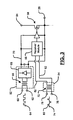
- a ballast 200 for a fluorescent lamp may implement the present invention.
- the ballast 200 includes the transformer 106, a full or half-wave rectifier 108, an electrolytic capacitor 202, a ballast logic module 204, and the pattern recognition receiver module 114.
- the electrolytic capacitor 202 may be used to filter or smooth voltage.
- the ballast logic module 204 includes the sender module 104.
- the rectifier 108 and the pattern recognition receiver module 114 may be implemented by an integrated circuit (IC) 206.
- the pattern recognition receiver module 114 may share input pins of the rectifier 108.
- the sender module 104 generates the input power signal 110 for driving the high side transistor 58 as described in FIGS. 4 and 6 .
- the ballast logic module 204 generates a low side transistor input signal 208 for driving a low side transistor 210.
- the ballast logic module 204 switches the transistors 58 and 210 ON and OFF to vary current and/or voltage to a fluorescent light 212 during startup and/or operation.
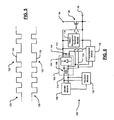
- the fluorescent light 212 includes a sealed glass tube 214 that contains a first material such as mercury and a first inert gas such as argon, which are both generally identified at 216.
- the tube 214 is pressurized.
- Phosphor powder 218 may be coated along an inner surface of the tube 214.
- the tube 214 includes electrodes 220A and 220B ( referred to collectively as electrodes 220) that are located at opposite ends of the tube 214. Power is supplied to the electrodes 220 according to the ON or OFF statuses of the transistors 58 and 210.
- ballast logic module 204 regulates power both during and after startup.
- An exemplary fluorescent light and ballast that may implement the ballast logic module 204 is described in further detail in U.S. Patent Application No. 11/112,808, filed on April 22, 2005 , which is hereby incorporated by reference in its entirety.
- the ballast 200 may include a delay matching module 222.
- the operation of the transistor 58 may be delayed during the processing of input power signal 110.
- the delay matching module 222 adds the delay to the transistor 210.
- the delay matching module 222 offsets the response of the transistor 210 to compensate for the delay.
- the ballast 200 may include a calibration circuit to adjust the delay dynamically.
- the ballast logic module 204, sender module 104, or other components of the ballast 200 may determine the delay and adjust the delay matching module 222 accordingly.
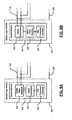
- the ballast logic module 204 includes a high frequency oscillator 300 and a digital state machine 302.
- the sender module 104 includes the high frequency oscillator 300 and the digital state machine 302.
- the digital stage machine 302 generates the power input signal 110, In other words, the digital state machine 302 outputs the power input signal 110 at an output frequency according to the oscillator 300.
- the ballast logic module changes the output frequency by changing a counter value of the digital state machine 302.
- the ballast logic module 204 may further include a digital interpolator 304.
- the ballast logic module 204 may implement a more complex frequency scanning algorithm in the digital domain. Further, the ballast logic module 204 may implement spread-spectrum technology by dithering the counter value of the digital state machine 302 around a final average target oscillator frequency. An alternative implementation of the ballast logic module 204 is shown in FIG. 8B .
- the ballast logic module 204 operates in the digital domain to generate the disturbance pattern in the power input signal 110.
- the ballast logic module 204 may generate the disturbance pattern in anticipation of certain events.
- the ballast logic module 204 may generate a square wave disturbance signal slightly early to avoid generating extremely narrow pulses at a boundary of the normal pulses and the lower frequency (i.e. disturbance) pulses.
- the ballast logic module 204 is able to accurately adjust the lower frequency pulses so that pulse edges are precisely located. In other words, the normal pulses can resume immediately after the disturbance pulses.
- a clock signal of the converter module 102 may be derived from the digital state machine 302. In this manner, the ballast logic module 204 can synchronize pulses of the converter module 102 with the disturbance pulses.
- the ballast module 204 may include one or more status modules 310.
- the status module 310 may implement an algorithm that detects lamp end of life based on lamp ignition retries. In this manner, the ballast logic module 204 can avoid damage due to overheating. Additionally, the status module 310 may implement over-voltage lamp detection by scanning startup voltage.
Landscapes
- Engineering & Computer Science (AREA)
- Power Engineering (AREA)
- Dc-Dc Converters (AREA)
- Electronic Switches (AREA)
- Logic Circuits (AREA)
- Inverter Devices (AREA)
Applications Claiming Priority (3)
| Application Number | Priority Date | Filing Date | Title |
|---|---|---|---|
| US72086605P | 2005-09-27 | 2005-09-27 | |
| US76273806P | 2006-01-27 | 2006-01-27 | |
| US11/367,638 US7619447B2 (en) | 2005-09-27 | 2006-03-03 | High voltage high side transistor driver |
Publications (2)
| Publication Number | Publication Date |
|---|---|
| EP1768257A1 EP1768257A1 (en) | 2007-03-28 |
| EP1768257B1 true EP1768257B1 (en) | 2014-06-18 |
Family
ID=37036902
Family Applications (1)
| Application Number | Title | Priority Date | Filing Date |
|---|---|---|---|
| EP06016937.2A Not-in-force EP1768257B1 (en) | 2005-09-27 | 2006-08-14 | High voltage high side transistor driver |
Country Status (6)
| Country | Link |
|---|---|
| US (2) | US7619447B2 (https=) |
| EP (1) | EP1768257B1 (https=) |
| JP (1) | JP2007097153A (https=) |
| CN (1) | CN1942037B (https=) |
| SG (1) | SG131017A1 (https=) |
| TW (1) | TWI394368B (https=) |
Families Citing this family (19)
| Publication number | Priority date | Publication date | Assignee | Title |
|---|---|---|---|---|
| US7777370B2 (en) * | 2007-05-03 | 2010-08-17 | Honeywell International Inc. | Integrated gate drive for use in control and protection of power modules |
| US7804697B2 (en) | 2007-12-11 | 2010-09-28 | Cirrus Logic, Inc. | History-independent noise-immune modulated transformer-coupled gate control signaling method and apparatus |
| US7656687B2 (en) | 2007-12-11 | 2010-02-02 | Cirrus Logic, Inc. | Modulated transformer-coupled gate control signaling method and apparatus |
| US8008898B2 (en) | 2008-01-30 | 2011-08-30 | Cirrus Logic, Inc. | Switching regulator with boosted auxiliary winding supply |
| US7796076B2 (en) * | 2008-02-26 | 2010-09-14 | Cirrus Logic, Inc. | Transformer-isolated analog-to-digital converter (ADC) feedback apparatus and method |
| US8008902B2 (en) | 2008-06-25 | 2011-08-30 | Cirrus Logic, Inc. | Hysteretic buck converter having dynamic thresholds |
| US8847719B2 (en) | 2008-07-25 | 2014-09-30 | Cirrus Logic, Inc. | Transformer with split primary winding |
| US8816653B2 (en) * | 2008-09-25 | 2014-08-26 | Infineon Technologies Austria Ag | Circuit including a transformer for driving a semiconductor switching element |
| US8222872B1 (en) | 2008-09-30 | 2012-07-17 | Cirrus Logic, Inc. | Switching power converter with selectable mode auxiliary power supply |
| US8331114B2 (en) * | 2009-02-10 | 2012-12-11 | System General Corporation | Flyback power converters having a high side driving circuit |
| US8212493B2 (en) | 2009-06-30 | 2012-07-03 | Cirrus Logic, Inc. | Low energy transfer mode for auxiliary power supply operation in a cascaded switching power converter |
| US8198874B2 (en) | 2009-06-30 | 2012-06-12 | Cirrus Logic, Inc. | Switching power converter with current sensing transformer auxiliary power supply |
| US9088220B2 (en) | 2012-08-03 | 2015-07-21 | Cooper Technologies Company | Combined low power isolated power supply with isolated data transfer |
| WO2014135209A1 (en) * | 2013-03-06 | 2014-09-12 | SiEVA | Apparatus for high side transistor bridge driver |
| DE102013205706A1 (de) * | 2013-03-28 | 2014-10-02 | Fraunhofer-Gesellschaft zur Förderung der angewandten Forschung e.V. | Leistungselektronische schaltung und system mit derselben |
| US10051701B2 (en) | 2014-07-16 | 2018-08-14 | Philips Lighting Holding B.V. | Systems and methods for maintaining dimmer behavior in a low-power lamp assembly |
| US9966837B1 (en) | 2016-07-08 | 2018-05-08 | Vpt, Inc. | Power converter with circuits for providing gate driving |
| US11183835B2 (en) * | 2019-07-16 | 2021-11-23 | Infineon Technologies Austria Ag | Short circuit detection and protection for a gate driver circuit and methods of detecting the same using logic analysis |
| WO2025049969A1 (en) * | 2023-08-31 | 2025-03-06 | Texas Instruments Incorporated | Opto-emulator |
Family Cites Families (14)
| Publication number | Priority date | Publication date | Assignee | Title |
|---|---|---|---|---|
| FR2668664B1 (fr) | 1990-10-25 | 1995-06-09 | Dassault Electronique | Convertisseur de tension a decoupage, a commande perfectionnee. |
| US5272398A (en) | 1991-09-12 | 1993-12-21 | Otis Elevator Company | Driver for power field-controlled switches with refreshed power supply providing stable on/off switching |
| FI90605C (fi) | 1991-12-09 | 1994-02-25 | Abb Stroemberg Drives Oy | Puolijohdekytkimen ohjauspiiri |
| US5309066A (en) | 1992-05-29 | 1994-05-03 | Jorck & Larsen A/S | Solid state ballast for fluorescent lamps |
| US5399913A (en) | 1992-09-02 | 1995-03-21 | Exide Elecronics Corp. | Gate-drive circuit |
| FR2771590B1 (fr) | 1997-11-21 | 2003-01-03 | Sgs Thomson Microelectronics | Circuit de commande de lampe fluorescente |
| US5900683A (en) | 1997-12-23 | 1999-05-04 | Ford Global Technologies, Inc. | Isolated gate driver for power switching device and method for carrying out same |
| IT1318952B1 (it) | 2000-10-02 | 2003-09-19 | St Microelectronics Srl | Circuito di protezione alle alte correnti in convertitori perilluminazione |
| DE10106438A1 (de) | 2001-02-09 | 2002-08-14 | Patent Treuhand Ges Fuer Elektrische Gluehlampen Mbh | Vorschaltgerät zum Betrieb von elektrischen Lampen |
| CN1579115A (zh) | 2002-02-20 | 2005-02-09 | 松下电器产业株式会社 | 无电极放电灯点亮装置、灯泡形无电极荧光灯和放电灯点亮装置 |
| DE102004047372A1 (de) * | 2004-09-29 | 2006-03-30 | Patent-Treuhand-Gesellschaft für elektrische Glühlampen mbH | Wandlerschaltung mit Klasse-E-Konvertermodulen |
| US7176723B2 (en) * | 2005-02-18 | 2007-02-13 | Semiconductor Components Industries Llc | Translator circuit and method therefor |
| US7560866B2 (en) | 2005-04-18 | 2009-07-14 | Marvell World Trade Ltd. | Control system for fluorescent light fixture |
| US7405595B2 (en) * | 2005-11-16 | 2008-07-29 | System General Corp. | High-side transistor driver having positive feedback for improving speed and power saving |
-
2006
- 2006-03-03 US US11/367,638 patent/US7619447B2/en not_active Expired - Fee Related
- 2006-08-14 EP EP06016937.2A patent/EP1768257B1/en not_active Not-in-force
- 2006-08-24 CN CN2006101099217A patent/CN1942037B/zh not_active Expired - Fee Related
- 2006-08-25 JP JP2006229479A patent/JP2007097153A/ja active Pending
- 2006-08-25 TW TW095131328A patent/TWI394368B/zh not_active IP Right Cessation
- 2006-08-29 SG SG200605783-0A patent/SG131017A1/en unknown
-
2009
- 2009-11-16 US US12/619,198 patent/US8063670B2/en active Active
Also Published As
| Publication number | Publication date |
|---|---|
| TW200713816A (en) | 2007-04-01 |
| TWI394368B (zh) | 2013-04-21 |
| CN1942037B (zh) | 2012-04-18 |
| CN1942037A (zh) | 2007-04-04 |
| US7619447B2 (en) | 2009-11-17 |
| JP2007097153A (ja) | 2007-04-12 |
| SG131017A1 (en) | 2007-04-26 |
| US20070070653A1 (en) | 2007-03-29 |
| EP1768257A1 (en) | 2007-03-28 |
| US20100060327A1 (en) | 2010-03-11 |
| US8063670B2 (en) | 2011-11-22 |
Similar Documents
| Publication | Publication Date | Title |
|---|---|---|
| US8063670B2 (en) | High voltage high side transistor driver | |
| US7161818B2 (en) | High frequency excitation system | |
| EP3195461B1 (en) | Electrodeless fluorescent ballast driving circuit and resonance circuit with added filtration and protection | |
| JP2010283998A (ja) | ゼロ電流スイッチングおよび任意周波数のパルス幅変調を利用した共振インバータの駆動方法 | |
| EP2030486B1 (en) | Lamp driving circuit | |
| JP2007508799A (ja) | 電力変換器 | |
| JP4528616B2 (ja) | ガス放電ランプ用ドライバ | |
| JP3851092B2 (ja) | ハーフブリッジ形インバータ回路 | |
| JP2009048935A (ja) | 交流電源装置 | |
| US20080157692A1 (en) | Discharge lamp lighting circuit | |
| JP3758305B2 (ja) | 照明用点灯装置 | |
| US6473320B2 (en) | Voltage converter circuit with self-oscillating half-bridge configuration and with protection against hard switching | |
| JP4193798B2 (ja) | 放電管点灯装置 | |
| JP2007059155A (ja) | 冷陰極管点灯装置、該冷陰極管点灯装置に用いられる管電流検出回路、管電流制御方法、及び集積回路 | |
| US20060125414A1 (en) | Lamp lighting circuit | |
| HK1105105A (en) | High voltage high side transistor driver | |
| KR100454423B1 (ko) | 냉음극관 밝기 제어장치 | |
| US8274235B2 (en) | Inverter device and driving method thereof | |
| JP2009026497A (ja) | 放電灯点灯回路 | |
| US7615934B2 (en) | High efficiency resonant ballast | |
| WO2011001340A1 (en) | Circuit for converting dc into ac pulsed voltage | |
| KR200239224Y1 (ko) | 스위치 모드 전원 공급 장치 | |
| JPH0896972A (ja) | 放電灯点灯装置 | |
| Yeon et al. | A New Dimming Method for Electrodeless Lamps | |
| JPH10228989A (ja) | 無電極放電灯点灯装置 |
Legal Events
| Date | Code | Title | Description |
|---|---|---|---|
| PUAI | Public reference made under article 153(3) epc to a published international application that has entered the european phase |
Free format text: ORIGINAL CODE: 0009012 |
|
| AK | Designated contracting states |
Kind code of ref document: A1 Designated state(s): AT BE BG CH CY CZ DE DK EE ES FI FR GB GR HU IE IS IT LI LT LU LV MC NL PL PT RO SE SI SK TR |
|
| AX | Request for extension of the european patent |
Extension state: AL BA HR MK YU |
|
| 17P | Request for examination filed |
Effective date: 20070807 |
|
| 17Q | First examination report despatched |
Effective date: 20070907 |
|
| AKX | Designation fees paid |
Designated state(s): DE FR GB |
|
| GRAP | Despatch of communication of intention to grant a patent |
Free format text: ORIGINAL CODE: EPIDOSNIGR1 |
|
| INTG | Intention to grant announced |
Effective date: 20140108 |
|
| GRAS | Grant fee paid |
Free format text: ORIGINAL CODE: EPIDOSNIGR3 |
|
| GRAA | (expected) grant |
Free format text: ORIGINAL CODE: 0009210 |
|
| AK | Designated contracting states |
Kind code of ref document: B1 Designated state(s): DE FR GB |
|
| REG | Reference to a national code |
Ref country code: GB Ref legal event code: FG4D |
|
| REG | Reference to a national code |
Ref country code: DE Ref legal event code: R096 Ref document number: 602006041930 Country of ref document: DE Effective date: 20140724 |
|
| REG | Reference to a national code |
Ref country code: DE Ref legal event code: R097 Ref document number: 602006041930 Country of ref document: DE |
|
| PLBE | No opposition filed within time limit |
Free format text: ORIGINAL CODE: 0009261 |
|
| STAA | Information on the status of an ep patent application or granted ep patent |
Free format text: STATUS: NO OPPOSITION FILED WITHIN TIME LIMIT |
|
| 26N | No opposition filed |
Effective date: 20150319 |
|
| REG | Reference to a national code |
Ref country code: FR Ref legal event code: PLFP Year of fee payment: 11 |
|
| REG | Reference to a national code |
Ref country code: FR Ref legal event code: PLFP Year of fee payment: 12 |
|
| REG | Reference to a national code |
Ref country code: FR Ref legal event code: PLFP Year of fee payment: 13 |
|
| PGFP | Annual fee paid to national office [announced via postgrant information from national office to epo] |
Ref country code: FR Payment date: 20190827 Year of fee payment: 14 |
|
| PGFP | Annual fee paid to national office [announced via postgrant information from national office to epo] |
Ref country code: GB Payment date: 20190829 Year of fee payment: 14 |
|
| REG | Reference to a national code |
Ref country code: DE Ref legal event code: R082 Ref document number: 602006041930 Country of ref document: DE Representative=s name: GRUENECKER PATENT- UND RECHTSANWAELTE PARTG MB, DE Ref country code: DE Ref legal event code: R081 Ref document number: 602006041930 Country of ref document: DE Owner name: MARVELL ASIA PTE, LTD., SG Free format text: FORMER OWNER: MARVELL WORLD TRADE LTD., BRITTONS HILL, SAINT MICHAEL, BB |
|
| REG | Reference to a national code |
Ref country code: GB Ref legal event code: 732E Free format text: REGISTERED BETWEEN 20200709 AND 20200715 |
|
| PGFP | Annual fee paid to national office [announced via postgrant information from national office to epo] |
Ref country code: DE Payment date: 20201029 Year of fee payment: 15 |
|
| GBPC | Gb: european patent ceased through non-payment of renewal fee |
Effective date: 20200814 |
|
| PG25 | Lapsed in a contracting state [announced via postgrant information from national office to epo] |
Ref country code: FR Free format text: LAPSE BECAUSE OF NON-PAYMENT OF DUE FEES Effective date: 20200831 |
|
| PG25 | Lapsed in a contracting state [announced via postgrant information from national office to epo] |
Ref country code: GB Free format text: LAPSE BECAUSE OF NON-PAYMENT OF DUE FEES Effective date: 20200814 |
|
| REG | Reference to a national code |
Ref country code: DE Ref legal event code: R119 Ref document number: 602006041930 Country of ref document: DE |
|
| PG25 | Lapsed in a contracting state [announced via postgrant information from national office to epo] |
Ref country code: DE Free format text: LAPSE BECAUSE OF NON-PAYMENT OF DUE FEES Effective date: 20220301 |