EP1748488A1 - Mémoire de semi-conducteur - Google Patents
Mémoire de semi-conducteur Download PDFInfo
- Publication number
- EP1748488A1 EP1748488A1 EP05737197A EP05737197A EP1748488A1 EP 1748488 A1 EP1748488 A1 EP 1748488A1 EP 05737197 A EP05737197 A EP 05737197A EP 05737197 A EP05737197 A EP 05737197A EP 1748488 A1 EP1748488 A1 EP 1748488A1
- Authority
- EP
- European Patent Office
- Prior art keywords
- interlayer insulating
- plug
- insulating film
- phase change
- material layer
- Prior art date
- Legal status (The legal status is an assumption and is not a legal conclusion. Google has not performed a legal analysis and makes no representation as to the accuracy of the status listed.)
- Granted
Links
- 239000004065 semiconductor Substances 0.000 title claims description 78
- 239000010410 layer Substances 0.000 claims abstract description 155
- 239000012790 adhesive layer Substances 0.000 claims abstract description 123
- 230000015654 memory Effects 0.000 claims abstract description 100
- 150000004767 nitrides Chemical class 0.000 claims abstract description 45
- 230000001681 protective effect Effects 0.000 claims abstract description 26
- 239000011229 interlayer Substances 0.000 claims description 141
- 239000012782 phase change material Substances 0.000 claims description 56
- 230000002093 peripheral effect Effects 0.000 claims description 37
- 239000000758 substrate Substances 0.000 claims description 36
- 229910052719 titanium Inorganic materials 0.000 claims description 31
- 229910052581 Si3N4 Inorganic materials 0.000 claims description 28
- HQVNEWCFYHHQES-UHFFFAOYSA-N silicon nitride Chemical compound N12[Si]34N5[Si]62N3[Si]51N64 HQVNEWCFYHHQES-UHFFFAOYSA-N 0.000 claims description 28
- 229910052782 aluminium Inorganic materials 0.000 claims description 21
- 229910052714 tellurium Inorganic materials 0.000 claims description 11
- 229910008484 TiSi Inorganic materials 0.000 claims description 10
- 150000001875 compounds Chemical class 0.000 claims description 9
- 229910052710 silicon Inorganic materials 0.000 claims description 7
- -1 TaSi Inorganic materials 0.000 claims description 6
- 229910010038 TiAl Inorganic materials 0.000 claims description 5
- 229910052715 tantalum Inorganic materials 0.000 claims description 5
- 230000015572 biosynthetic process Effects 0.000 claims description 4
- 229910052735 hafnium Inorganic materials 0.000 claims description 3
- 229910052726 zirconium Inorganic materials 0.000 claims description 3
- 239000010703 silicon Substances 0.000 claims description 2
- 239000004020 conductor Substances 0.000 claims 1
- 239000000463 material Substances 0.000 abstract description 123
- 150000004770 chalcogenides Chemical class 0.000 abstract description 115
- 230000008859 change Effects 0.000 abstract description 48
- 238000004519 manufacturing process Methods 0.000 abstract description 40
- VYPSYNLAJGMNEJ-UHFFFAOYSA-N Silicium dioxide Chemical compound O=[Si]=O VYPSYNLAJGMNEJ-UHFFFAOYSA-N 0.000 abstract description 34
- 229910052814 silicon oxide Inorganic materials 0.000 abstract description 30
- 230000032798 delamination Effects 0.000 abstract description 20
- 238000002844 melting Methods 0.000 abstract description 10
- 230000008018 melting Effects 0.000 abstract description 10
- 229910052751 metal Inorganic materials 0.000 abstract description 10
- 239000002184 metal Substances 0.000 abstract description 10
- 238000000859 sublimation Methods 0.000 abstract description 9
- 230000008022 sublimation Effects 0.000 abstract description 9
- 150000002739 metals Chemical class 0.000 abstract description 4
- 239000010408 film Substances 0.000 description 261
- 238000000034 method Methods 0.000 description 89
- 239000012071 phase Substances 0.000 description 43
- WFKWXMTUELFFGS-UHFFFAOYSA-N tungsten Chemical compound [W] WFKWXMTUELFFGS-UHFFFAOYSA-N 0.000 description 40
- 229910052721 tungsten Inorganic materials 0.000 description 40
- 239000010937 tungsten Substances 0.000 description 40
- 230000008569 process Effects 0.000 description 39
- 229910000618 GeSbTe Inorganic materials 0.000 description 36
- 239000010936 titanium Substances 0.000 description 24
- 238000001312 dry etching Methods 0.000 description 19
- RTAQQCXQSZGOHL-UHFFFAOYSA-N Titanium Chemical compound [Ti] RTAQQCXQSZGOHL-UHFFFAOYSA-N 0.000 description 13
- XAGFODPZIPBFFR-UHFFFAOYSA-N aluminium Chemical compound [Al] XAGFODPZIPBFFR-UHFFFAOYSA-N 0.000 description 9
- 238000010438 heat treatment Methods 0.000 description 9
- XKRFYHLGVUSROY-UHFFFAOYSA-N Argon Chemical compound [Ar] XKRFYHLGVUSROY-UHFFFAOYSA-N 0.000 description 8
- 238000010586 diagram Methods 0.000 description 7
- 238000002955 isolation Methods 0.000 description 6
- 230000001070 adhesive effect Effects 0.000 description 5
- 238000007796 conventional method Methods 0.000 description 5
- 238000009792 diffusion process Methods 0.000 description 5
- 230000000694 effects Effects 0.000 description 5
- 238000004544 sputter deposition Methods 0.000 description 5
- 230000003746 surface roughness Effects 0.000 description 5
- 239000000853 adhesive Substances 0.000 description 4
- 229910052786 argon Inorganic materials 0.000 description 4
- 238000002425 crystallisation Methods 0.000 description 4
- 230000008025 crystallization Effects 0.000 description 4
- 238000000151 deposition Methods 0.000 description 4
- 238000003795 desorption Methods 0.000 description 4
- 239000007789 gas Substances 0.000 description 4
- 230000003647 oxidation Effects 0.000 description 4
- 238000007254 oxidation reaction Methods 0.000 description 4
- 238000004611 spectroscopical analysis Methods 0.000 description 4
- IJGRMHOSHXDMSA-UHFFFAOYSA-N Atomic nitrogen Chemical compound N#N IJGRMHOSHXDMSA-UHFFFAOYSA-N 0.000 description 3
- RYGMFSIKBFXOCR-UHFFFAOYSA-N Copper Chemical compound [Cu] RYGMFSIKBFXOCR-UHFFFAOYSA-N 0.000 description 3
- 229910052802 copper Inorganic materials 0.000 description 3
- 239000010949 copper Substances 0.000 description 3
- 229910001873 dinitrogen Inorganic materials 0.000 description 3
- 238000005530 etching Methods 0.000 description 3
- 229910021420 polycrystalline silicon Inorganic materials 0.000 description 3
- 229920005591 polysilicon Polymers 0.000 description 3
- 238000012360 testing method Methods 0.000 description 3
- GWEVSGVZZGPLCZ-UHFFFAOYSA-N Titan oxide Chemical compound O=[Ti]=O GWEVSGVZZGPLCZ-UHFFFAOYSA-N 0.000 description 2
- QVGXLLKOCUKJST-UHFFFAOYSA-N atomic oxygen Chemical compound [O] QVGXLLKOCUKJST-UHFFFAOYSA-N 0.000 description 2
- 230000008901 benefit Effects 0.000 description 2
- 230000001413 cellular effect Effects 0.000 description 2
- 229910052681 coesite Inorganic materials 0.000 description 2
- 229910052906 cristobalite Inorganic materials 0.000 description 2
- 239000003989 dielectric material Substances 0.000 description 2
- 230000002708 enhancing effect Effects 0.000 description 2
- 239000012535 impurity Substances 0.000 description 2
- 230000001965 increasing effect Effects 0.000 description 2
- 238000003780 insertion Methods 0.000 description 2
- 230000037431 insertion Effects 0.000 description 2
- 238000005259 measurement Methods 0.000 description 2
- 239000001301 oxygen Substances 0.000 description 2
- 229910052760 oxygen Inorganic materials 0.000 description 2
- 230000008672 reprogramming Effects 0.000 description 2
- 239000000377 silicon dioxide Substances 0.000 description 2
- 229910052682 stishovite Inorganic materials 0.000 description 2
- 239000000126 substance Substances 0.000 description 2
- OGIDPMRJRNCKJF-UHFFFAOYSA-N titanium oxide Inorganic materials [Ti]=O OGIDPMRJRNCKJF-UHFFFAOYSA-N 0.000 description 2
- 229910052905 tridymite Inorganic materials 0.000 description 2
- 238000001947 vapour-phase growth Methods 0.000 description 2
- 229910001080 W alloy Inorganic materials 0.000 description 1
- 230000004075 alteration Effects 0.000 description 1
- 238000004458 analytical method Methods 0.000 description 1
- 229910052787 antimony Inorganic materials 0.000 description 1
- 230000004888 barrier function Effects 0.000 description 1
- 230000015556 catabolic process Effects 0.000 description 1
- 238000004140 cleaning Methods 0.000 description 1
- 230000003247 decreasing effect Effects 0.000 description 1
- 238000006731 degradation reaction Methods 0.000 description 1
- 230000002349 favourable effect Effects 0.000 description 1
- 230000006870 function Effects 0.000 description 1
- 229910052732 germanium Inorganic materials 0.000 description 1
- 238000002513 implantation Methods 0.000 description 1
- 230000006872 improvement Effects 0.000 description 1
- 238000005268 plasma chemical vapour deposition Methods 0.000 description 1
- 229920000515 polycarbonate Polymers 0.000 description 1
- 239000004417 polycarbonate Substances 0.000 description 1
- 238000010791 quenching Methods 0.000 description 1
- 238000000926 separation method Methods 0.000 description 1
- 239000007787 solid Substances 0.000 description 1
- 239000010409 thin film Substances 0.000 description 1
- MAKDTFFYCIMFQP-UHFFFAOYSA-N titanium tungsten Chemical compound [Ti].[W] MAKDTFFYCIMFQP-UHFFFAOYSA-N 0.000 description 1
Images


Classifications
-
- H—ELECTRICITY
- H10—SEMICONDUCTOR DEVICES; ELECTRIC SOLID-STATE DEVICES NOT OTHERWISE PROVIDED FOR
- H10N—ELECTRIC SOLID-STATE DEVICES NOT OTHERWISE PROVIDED FOR
- H10N70/00—Solid-state devices having no potential barriers, and specially adapted for rectifying, amplifying, oscillating or switching
- H10N70/20—Multistable switching devices, e.g. memristors
- H10N70/231—Multistable switching devices, e.g. memristors based on solid-state phase change, e.g. between amorphous and crystalline phases, Ovshinsky effect
-
- H—ELECTRICITY
- H10—SEMICONDUCTOR DEVICES; ELECTRIC SOLID-STATE DEVICES NOT OTHERWISE PROVIDED FOR
- H10B—ELECTRONIC MEMORY DEVICES
- H10B63/00—Resistance change memory devices, e.g. resistive RAM [ReRAM] devices
- H10B63/30—Resistance change memory devices, e.g. resistive RAM [ReRAM] devices comprising selection components having three or more electrodes, e.g. transistors
-
- H—ELECTRICITY
- H10—SEMICONDUCTOR DEVICES; ELECTRIC SOLID-STATE DEVICES NOT OTHERWISE PROVIDED FOR
- H10N—ELECTRIC SOLID-STATE DEVICES NOT OTHERWISE PROVIDED FOR
- H10N70/00—Solid-state devices having no potential barriers, and specially adapted for rectifying, amplifying, oscillating or switching
- H10N70/011—Manufacture or treatment of multistable switching devices
- H10N70/061—Shaping switching materials
- H10N70/063—Shaping switching materials by etching of pre-deposited switching material layers, e.g. lithography
-
- H—ELECTRICITY
- H10—SEMICONDUCTOR DEVICES; ELECTRIC SOLID-STATE DEVICES NOT OTHERWISE PROVIDED FOR
- H10N—ELECTRIC SOLID-STATE DEVICES NOT OTHERWISE PROVIDED FOR
- H10N70/00—Solid-state devices having no potential barriers, and specially adapted for rectifying, amplifying, oscillating or switching
- H10N70/801—Constructional details of multistable switching devices
- H10N70/821—Device geometry
- H10N70/826—Device geometry adapted for essentially vertical current flow, e.g. sandwich or pillar type devices
-
- H—ELECTRICITY
- H10—SEMICONDUCTOR DEVICES; ELECTRIC SOLID-STATE DEVICES NOT OTHERWISE PROVIDED FOR
- H10N—ELECTRIC SOLID-STATE DEVICES NOT OTHERWISE PROVIDED FOR
- H10N70/00—Solid-state devices having no potential barriers, and specially adapted for rectifying, amplifying, oscillating or switching
- H10N70/801—Constructional details of multistable switching devices
- H10N70/841—Electrodes
- H10N70/8413—Electrodes adapted for resistive heating
-
- H—ELECTRICITY
- H10—SEMICONDUCTOR DEVICES; ELECTRIC SOLID-STATE DEVICES NOT OTHERWISE PROVIDED FOR
- H10N—ELECTRIC SOLID-STATE DEVICES NOT OTHERWISE PROVIDED FOR
- H10N70/00—Solid-state devices having no potential barriers, and specially adapted for rectifying, amplifying, oscillating or switching
- H10N70/801—Constructional details of multistable switching devices
- H10N70/881—Switching materials
- H10N70/882—Compounds of sulfur, selenium or tellurium, e.g. chalcogenides
- H10N70/8825—Selenides, e.g. GeSe
-
- H—ELECTRICITY
- H10—SEMICONDUCTOR DEVICES; ELECTRIC SOLID-STATE DEVICES NOT OTHERWISE PROVIDED FOR
- H10N—ELECTRIC SOLID-STATE DEVICES NOT OTHERWISE PROVIDED FOR
- H10N70/00—Solid-state devices having no potential barriers, and specially adapted for rectifying, amplifying, oscillating or switching
- H10N70/801—Constructional details of multistable switching devices
- H10N70/881—Switching materials
- H10N70/882—Compounds of sulfur, selenium or tellurium, e.g. chalcogenides
- H10N70/8828—Tellurides, e.g. GeSbTe
Definitions
- the present invention relates to a technique that is effective when applied to semiconductor integrated circuit devices which employ phase change memory cells formed of a phase change material such as chalcogenide.
- DRAM digital versatile disk
- SRAM static random access memory
- flash memory flash memory
- a DRAM provides large capacity but its access speed is low.
- a SRAM is high-speed memory, but is not suitable for forming a large capacity memory, since each cell requires a number of transistors (4 to 6 transistors) and hence it is difficult to produce highly integrated SRAM.
- DRAM and SRAM must continuously receive power to retain data; that is, they are volatile memories.
- Flash memory is a nonvolatile memory; it does not need to continuously receive power to electrically retain data.
- the flash memory is disadvantageous in that its program/erase count is limited to a maximum of approximately 10 5 and its reprogramming speed is a few orders of magnitude lower than those of other memories. Since each memory (described above) has its disadvantage, it is current practice to select suitable memory depending on the application.
- Phase change memory uses a chalcogenide material, which is also used by CD-RWs and DVDs. Like these disks, phase change memory stores data by assuming two states: a crystalline state and an amorphous state. However, they differ in how data is written to or read from them. Specifically, whereas a laser is used to write to or read from CD-RWs and DVDs, the Joule heat generated by an electrical current is used to write data to the phase change memory and the change in the resistance of the memory due to the phase change is read as a data value.
- phase change memory When a chalcogenide material is amorphized, such a reset pulse is applied that causes the chalcogenide material to be rapidly quenched after it is heated to a melting point or more.
- the melting point is, for example, 600°C
- the quench time (t1) is, for example, 2 nsec.
- a set pulse is applied to the memory so as to maintain the chalcogenide material at a temperature between its crystallization point and melting point.
- the crystallization point is, for example, 400°C
- the time (t2) required for the crystallization is, for example, 50 nsec.
- phase change memory is that the resistance value of the chalcogenide material (of the phase change memory) varies by two to three orders of magnitude depending on its crystallization state. Since (the change in) the resistance value is used as a signal, the read signal is large, facilitating the sense operation and hence increasing the speed of the read operation.
- Another feature of the phase change memory is that it can be reprogrammed 10 12 times, which is an advantage over flash memory. Still another feature of the phase change memory is that it can operate at a low voltage and low power, which allows it to be formed on the same chip as logic circuitry. Therefore, phase change memory is suitable for use in mobile devices.
- a select transistor is formed on a semiconductor substrate by a known manufacturing method (not shown).
- the select transistor is made up of a MOS transistor or bipolar transistor.
- an interlayer insulating film 1 made up of a silicon oxide film is deposited and a plug 2 of, for example, tungsten is formed in the interlayer insulating film 1 by a known manufacturing method. This plug is used to electrically connect between the select transistor and the phase change material layer overlying the select transistor.
- a chalcogenide material layer 3 of, for example, GeSbTe, an upper electrode 4 of, for example, tungsten, and a hard mask 5 made up of, for example, a silicon oxide film are sequentially deposited, forming the structure shown in Fig. 3.
- the hard mask 5, the upper electrode 4, and the chalcogenide material layer 3 are processed by a known lithographic technique and dry etching technique, as shown in Fig. 4.
- an interlayer insulating film 6 is deposited, as shown in Fig. 5.
- a wiring layer electrically connected to the upper electrode 4 is formed on the interlayer insulating film 6, and a plurality of other wiring layers are formed on the wiring layer on the interlayer insulating film 6, completing formation of phase change memory (not shown).
- phase change memory There are two problems that make it difficult to manufacture phase change memory: the low adhesive strength and the low thermal stability of the chalcogenide material. How the manufacturing process is affected by each problem will be specifically described. First, since chalcogenide material has low adhesive strength, it tends to delaminate (or peel) during the manufacturing process. Since the chalcogenide material is heated to its melting point or a higher temperature when the phase change memory is in operation (as described above), the plug and the upper electrode in contact with the chalcogenide material must be formed of a high melting point metal. For example, tungsten is a high melting point metal conventionally used in semiconductor integrated circuit devices.
- chalcogenide material layer
- high melting point metals such as tungsten
- the chalcogenide material also exhibits low adhesion to silicon oxide films, it also tends to delaminate at its interface with the interlayer insulating film. It is obvious that the manufacturing process described with reference to Figs. 3 to 5 produces a phase change memory cell in which the chalcogenide material exhibits low adhesion at its upper and lower interfaces. Therefore, there is a need for a means of enhancing the adhesive strength of the chalcogenide material (at these interfaces).
- Figs. 6A to 6C show results of thermal desorption spectrometry of a GeSbTe film. This analysis was conducted in ultrahigh vacuum (approximately, 10 -7 Pa). When the GeSbTe film was heated to approximately 300°C, the elements Ge, Sb, and Te sublimed at the same time, as shown in the figures. The sample was further heated to 500°C and then cooled to room temperature. After this, we retrieved the sample and found that the GeSbTe film had completely disappeared. Thus, chalcogenide material has very low thermal stability.
- Fig. 7 is a graph showing the sublimation characteristics of a GeSbTe film, wherein the horizontal axis represents temperature and the vertical axis represents pressure. Specifically, the temperature and pressure at which the GeSbTe film was heat-treated were varied.
- each open circle indicates a condition in which the GeSbTe film did not sublime, while each solid circle indicates a condition in which the GeSbTe film sublimed.
- the lower the pressure under which the GeSbTe film was heat-treated the lower the temperature at which it sublimed.
- a manufacturing process of a semiconductor integrated circuit device performs, for example, chemical vapor phase growth at a pressure of approximately 10 -1 -10 3 Pa and a temperature of approximately 400-700°C.
- the GeSbTe film will sublime if it is directly exposed to these conditions. In the manufacturing process described with reference to Figs.
- the interlayer insulating film 6 must be formed by chemical vapor phase growth, which is superior in terms of step coverage.
- the chalcogenide material layer 3 might sublime at its sidewalls. Therefore, there is a need for a means for maintaining the thermal stability of chalcogenide material even if a portion of the material is exposed.
- a semiconductor memory device comprising: a semiconductor substrate; a select transistor formed on a principal surface of the semiconductor substrate; an interlayer insulating film provided on the select transistor; a plug provided so as to penetrate through the interlayer insulating film, and electrically connected to the select transistor; a phase change material layer provided so as to extend over the interlayer insulating film, and connected with the plug; an upper electrode provided on the phase change material layer; and an adhesive layer provided between an under surface of the phase change material layer and top surfaces of the interlayer insulating film and the plug.
- a semiconductor memory device comprising: a semiconductor substrate; a select transistor formed on a principal surface of the semiconductor substrate; an interlayer insulating film provided on the select transistor; a plug provided so as to penetrate through the interlayer insulating film, the plug being electrically connected to the select transistor; a phase change material layer provided on the interlayer insulating film such that a portion of the phase change material layer is connected with the plug; an upper electrode provided on the phase change material layer; and a protective film formed on at least a sidewall of the phase change material layer and containing a silicon nitride.
- the adhesive layers formed over and under the chalcogenide material layer can prevent delamination of the chalcogenide material layer during the manufacturing process.
- the protective film formed on the sidewalls of the chalcogenide material layer can prevent sublimation of the chalcogenide material layer during the manufacturing process.
- a first means of the present invention is to form adhesive layers over and under the chalcogenide material (layer) so as to enhance the adhesive strength of the chalcogenide material (at its interfaces with the overlying and underlying layers).
- layers we formed GeSbTe films on SiO 2 films to a thickness of 100 nm, and performed a scratch test on these GeSbTe films to compare their delamination strength.
- a scratch test a thin film surface of a sample is scratched by an indenter while applying a load to the sample in the vertical direction, in order to determine the minimum load that cause delamination (referred to as the "critical delamination load"). The higher the critical delamination load, the higher the delamination strength.
- Fig. 8 shows the (critical delamination load) measurement results.
- the delamination strength of the GeSbTe film was extremely low when an adhesive layer was not inserted (between the GeSbTe film and the SiO 2 film). Further, insertion of a W layer did not lead to any improvement in the delamination strength of the GeSbTe film. This reflects the fact that chalcogenide material has low adhesion to high melting point metals.
- inserting an Al material layer increased the delamination strength of the GeSbTe film by a factor of 7-9, and inserting a Ti material layer enhanced the delamination strength by a factor of 10-15.
- insertion of an adhesive layer may be effective in enhancing the adhesive properties of the chalcogenide material.
- Ti material is superior to Al material as an adhesive layer.
- nitrides have higher adhesion to chalcogenide material than oxides, and individual metals have higher adhesion than oxides and nitrides.
- an interlayer insulating film 1 and a plug 2 are formed by a conventional technique.
- the following layers are sequentially deposited: an adhesive layer 7 of, for example, titanium; a chalcogenide material layer 3 of, for example, GeSbTe; an adhesive layer 8 of, for example, titanium; an upper electrode 4 of, for example, tungsten; and a hard mask 5 made up of, for example, a silicon oxide film.
- the hard mask 5, the upper electrode 4, the adhesive layer 8, the chalcogenide material layer 3, and the adhesive layer 7 are processed by a known lithographic technique and dry etching technique, forming the structure shown in Fig. 1.
- Figs. 9A and 9B show the temperature vs. resistance characteristics of GeSbTe films. Specifically, Fig. 9A shows the temperature vs. resistance characteristics of a GeSbTe film with no adhesive layer.
- Fig. 9A shows the resistance of the GeSbTe film. Since phase change memory uses the resistance value of the chalcogenide material layer as a signal, the larger the change in the resistance of the chalcogenide material between amorphous and crystalline states, the better.
- Fig. 9B shows the temperature vs. resistance characteristics of a GeSbTe film with a 2.5 nm thick adhesive layer of titanium.
- the GeSbTe film had low resistance even when it was in an amorphous state.
- the GeSbTe film was heated to approximately 200°C, so that the film crystallized. Then, the GeSbTe film was cooled.
- the resistance did not change much (between the amorphous and crystalline states). The reason for this may be that titanium within the adhesive layer diffused into the GeSbTe film. This indicates that if the adhesive layer has a small thickness, it may degrade the characteristics of the phase change memory.
- the thickness of the adhesive layers in phase change memory is preferably 5 nm or less although this may vary depending on the material of these layers. Further, the thickness of the adhesive layers is more preferably 2 nm or less to increase the ratio between the resistance values in amorphous and crystalline states.
- a current (as a set pulse or reset pulse) is supplied from the select transistor to the chalcogenide material (layer) through the plug to change the phase of the chalcogenide material.
- the adhesive layer at the interface between the chalcogenide material layer and the plug is preferably electrically conductive.
- the adhesive layer at the interface between the chalcogenide material layer and the upper electrode is also preferably conductive. Further, the smaller the regions used to change the phase of the chalcogenide material, the smaller the current required for reprogramming (the memory cell).
- Fig. 10 shows a phase change memory cell using an ideal material for the adhesive layers. Referring to the figure, a conductive adhesive layer 9 is formed at the interface between a chalcogenide material layer 3 and a plug 2; an insulative adhesive layer 10 is formed at the interface between the chalcogenide material layer 3 and an interlayer insulating film 1; and a conductive adhesive layer 11 is formed between the chalcogenide material layer 3 and an upper electrode 4.
- Examples of conductive adhesive layers include Ti, Al, Ta, Si, Ti nitride, Al nitride, Ta nitride, W nitride, TiSi, TaSi, WSi, TiW, TiAl nitride, TaSi nitride, TiSi nitride, and WSi nitride films. Further, since Te in chalcogenide material is reactive with Ti and Al, a layer formed of a compound of Ti and Te, or Al and Te, may be used as a conductive adhesive layer.
- Examples of insulative adhesive layers include Ti oxide, Al oxide, Ta oxide, Nb oxide, V oxide, Cr oxide, W oxide, Zr oxide, Hf oxide, and Si nitride films.
- the adhesive layer at the interface between the chalcogenide material layer and the interlayer insulating film need not necessarily be insulative (or nonconductive) if the chalcogenide material layer is not (fully) electrically connected to the interlayer insulating film. (This also reduces the regions used to cause a change in the phase of the chalcogenide material.)
- the adhesive layer may be a conductive layer having an island shape (i.e., a discontinuous conductive layer).
- the adhesive layer at the interface between the chalcogenide material layer and the plug and the adhesive layer at the interface between the chalcogenide material layer and the interlayer insulating film can be formed of the same material at the same time.
- an adhesive layer When an adhesive layer is formed to an island shape (or when a discontinuous adhesive layer is formed), its thickness is preferably 2 nm or less. Further, the thickness of the adhesive layer is more preferably 1 nm or less to increase or ensure the electrical discontinuity (between the chalcogenide material layer and the interlayer insulating film).
- the adhesive layers may be formed of titanium to a thickness of 0.5 nm.
- Patent Document 1 discloses means for using an adhesive layer to improve the adhesion between a chalcogenide material and a dielectric material. The present invention is different from this technique. As described above, in a phase change memory cell, the plug and the upper electrode must be formed of a high melting point metal such as tungsten.
- Patent Document 1 the above known technique (disclosed in Patent Document 1) is intended to insert an adhesive layer only between a chalcogenide material and an interlayer insulating film (formed of a dielectric material), which is distinctly different from the technique of the present invention.
- a second means of the present invention is to form a protective film on the sidewalls of the chalcogenide material layer to ensure the thermal stability of the chalcogenide material.
- An exemplary manufacturing process of the present invention will be described with reference to Fig. 11.
- an interlayer insulating film 1 and a plug 2 are formed by a conventional technique.
- a chalcogenide material layer 3 of, for example, GeSbTe, an upper electrode 4 of, for example, tungsten, and a hard mask 5 made up of, for example, a silicon oxide film are sequentially deposited.
- the hard mask 5, the upper electrode 4, and the chalcogenide material layer 3 are processed by a known lithographic technique and dry etching technique.
- a sidewall protective film 12 made up of, for example, a silicon nitride film is deposited, and an interlayer insulating film 6 is further deposited, as shown in Fig. 11.
- a sidewall protective film 12 made up of, for example, a silicon nitride film is deposited, and an interlayer insulating film 6 is further deposited, as shown in Fig. 11.
- Chalcogenide material sublimes when exposed to high temperature, low pressure conditions, as described with reference to Fig. 7. Therefore, the sidewall protective film must be formed under low temperature, high pressure conditions, which correspond to the upper left portion of Fig. 7. Especially, reducing the process temperature is effective in preventing sublimation of the chalcogenide material. Exemplary conditions are such that the pressure is 0.1 Pa or more and the temperature is 450°C or less, although this may vary depending on the chalcogenide material.
- the sidewall protective film is formed by plasma CVD, etc., since it must be formed at low temperature. If a silicon oxide film is used as the sidewall protective film, the sidewalls of the chalcogenide material (layer) are exposed to oxygen activated by the plasma. In this case, since chalcogenide material is easily oxidized, a portion of the chalcogenide material (layer) might be oxidized, resulting in degraded characteristics.
- a silicon nitride film is preferably used as the sidewall protective film, since it is "inactive against chalcogenide material" (or does not cause an oxidation problem such as that described above) and can be formed by CVD, which is a superior technique in terms of step coverage.
- Patent Document 2 discloses means for forming a protective film on the sidewalls of a chalcogenide material (layer) to prevent its sublimation.
- this technique is different from the present invention in that an oxide film is used as the protective film.
- a first embodiment of the present invention will be described with reference to Fig. 12.
- This embodiment provides an example in which conductive adhesive layers are formed both over and under the chalcogenide material layer.
- a semiconductor substrate 101 is provided, and a MOS transistor is formed on the substrate as a select transistor.
- trench isolation (or device separation) oxide films 102 for isolating the MOS transistor are formed in the surface of the semiconductor substrate 101 by a known selective oxidation technique or shallow trench isolation technique.
- the present embodiment uses the shallow trench isolation technique, which also can planarize the surface.
- isolation trenches are formed in the substrate by a known dry etching technique.
- an oxide film is deposited by a known CVD technique. Then, portions of the oxide film other than those in the trenches are polished (and thereby removed) by a known CMP technique, leaving the trench isolation oxide films 102 within the trenches.
- a gate oxide film 103 (for the MOS transistor) is grown by a known thermal oxidation technique. Then, a gate electrode 104 of polysilicon and a silicon nitride film 105 are (sequentially) deposited on the surface of the gate oxide film 103. After that, the gate is processed by a lithographic process and a dry etching process, and then impurities are implanted using the gate electrode and a resist as masks to form diffusion layers 106. It should be noted that although according to the present embodiment the gate electrode is made of polysilicon, it may be a polymetal gate (low resistance gate) having a laminated structure (metal/barrier metal/polysilicon). Then, a silicon nitride film 107 is deposited by CVD. (This film is used to help form self-aligned contacts.)
- an interlayer insulating film 108 made up of a silicon oxide film is deposited on the entire surface, and its surface roughness due to the gate electrode is removed by a known CMP technique, planarizing the surface. After that, plug contact holes are formed by a lithographic process and a dry etching process. At that time, to prevent exposure of the gate electrode, the interlayer insulating film 108 is processed under the so-called self-alignment conditions, that is, the interlayer insulating film 108 (i.e., a silicon oxide film) is selectively etched against the silicon nitride film 107 with a high selectivity ratio.
- the interlayer insulating film 108 i.e., a silicon oxide film
- the interlayer insulating film (or silicon oxide film) 108 is selectively dry etched against the silicon nitride film with a high selectivity ratio so as to leave the portions of the silicon nitride film on the top surfaces of the diffusion layers 106; and then the silicon nitride film is selectively dry etched against the silicon oxide film with a high selectivity ratio to remove the portions of the silicon nitride film left on the top surfaces of the diffusion layers 106.
- tungsten layers are formed buried in the plug contact holes, and tungsten plugs 109 are formed by a known CMP technique (that is, the tungsten layers are processed into tungsten plugs 109 by a known CMP technique).
- a tungsten layer is newly deposited to a thickness of 100 nm by sputtering and processed by a lithographic process and a dry etching process to form first wiring layers 110A and 110B.
- an interlayer insulating film 111 made up of a silicon oxide film is deposited on the entire surface, and its surface roughness due to the first wiring layers is removed by a known CMP technique, planarizing the surface.
- a plug contact hole is formed by a lithographic process and a dry etching process and filled with a tungsten layer.
- a tungsten plug 112 is formed by a known CMP technique.
- the following layers are sequentially deposited by a known sputtering technique: a conductive adhesive layer 113 of titanium having a thickness of 1 nm, a chalcogenide material layer 114 of GeSbTe having a thickness of 100 nm, a conductive adhesive layer 115 of titanium having a thickness of 1 nm, and an upper electrode 116 of tungsten having a thickness of 50 nm.
- a silicon oxide film 117 is deposited by a known CVD technique.
- the silicon oxide film 117, the upper electrode 116, the conductive adhesive layer 115, the chalcogenide material layer 114, and the conductive adhesive layer 113 are sequentially processed by a known lithographic process and dry etching process.
- the chalcogenide material may be crystallized by heat treatment after depositing the upper electrode 116 or the silicon oxide film 117.
- This heat treatment process can be performed under any conditions that allow the chalcogenide material to crystallize. Exemplary conditions are such that: the treatment atmosphere is an argon gas or nitrogen gas atmosphere; the treatment temperature is 200-600°C; and the treatment time is 1-10 minutes.
- the treatment atmosphere is an argon gas or nitrogen gas atmosphere
- the treatment temperature is 200-600°C
- the treatment time is 1-10 minutes.
- an interlayer insulating film 118 made up of a silicon oxide film is deposited on the entire surface, and its surface roughness is removed by a known CMP technique, planarizing the surface. After that, a plug contact hole is formed by a lithographic process and a dry etching process.
- a tungsten layer is buried in the plug contact hole, and a tungsten plug 119 is formed by a known CMP technique.
- an aluminum layer is deposited to a thickness of 200 nm and processed to form a second wiring layer 120. It should be noted that copper, which has lower resistance than aluminum, may be used instead of aluminum.
- adhesive layers are formed over and under the chalcogenide material layer, which increases the delamination strength of the chalcogenide material layer and thereby prevents its delamination during the manufacturing process.
- the adhesive layers may be conductive films such as Al, Ta, Si, Ti nitride, Al nitride, Ta nitride, W nitride, TiSi, TaSi, WSi, TiW, TiAl nitride, TaSi nitride, TiSi nitride, or WSi nitride films.
- the adhesive layers may be formed of a compound of Ti and Te or a compound of Al and Te. It should be noted that the present invention is not limited to the preferred embodiments described above. It is obvious that the present invention embraces all means described in the "Best Modes for Carrying out the Invention" section of this specification.
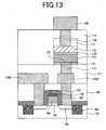
- a second embodiment of the present invention will be described with reference to Fig. 13.
- This embodiment provides an example in which: a conductive adhesive layer is formed at the interface between the chalcogenide material layer and the plug; an insulative adhesive layer is formed at the interface between the chalcogenide material layer and the interlayer insulating film; and a conductive adhesive layer is formed at the interface between the chalcogenide material layer and the upper electrode. Since the steps before and including the step of forming the tungsten plug 112 are the same as those described in connection with the first embodiment, a description of these steps is not provided herein.
- a process of forming an insulative adhesive layer 121 and a conductive adhesive layer 122 on the interlayer insulating film 111 and on the tungsten plus 112, respectively, in a self-aligned manner First, a titanium layer is deposited on the entire surfaces of the interlayer insulating film 111 and the tungsten plug 112 to a thickness of 3 nm by sputtering and then heat treated. Since titanium has a lower free energy of oxide formation than silicon, the portion of the titanium layer deposited on the interlayer insulating film 111 (that is, a silicon oxide film) reacts with oxygen in the underlying interlayer insulating film 111 to form a titanium oxide film.
- the insulative adhesive layer 121 is formed on the interlayer insulating film 111 and the conductive adhesive layer 122 is formed on the tungsten plug 112 in a self-aligned manner.
- the above heat treatment can be performed at any temperature that causes titanium to react with the silicon oxide film. However, 400°C or a higher temperature is preferred to form a favorable titanium oxide film. Further, the heat treatment is preferably performed in an inert atmosphere to prevent oxidation of the conductive adhesive layer. Exemplary conditions are such that: the treatment atmosphere is an argon gas atmosphere; the treatment temperature is 400-800°C; and the treatment time is 1-10 minutes.
- a chalcogenide material layer 114 of GeSbTe having a thickness of 100 nm, a conductive adhesive layer 115 of titanium having a thickness of 1 nm, and an upper electrode 116 of tungsten having a thickness 50 nm are sequentially deposited by a known sputtering technique.
- a silicon oxide film 117 is deposited by a known CVD technique.
- the silicon oxide film 117, the upper electrode 116, the conductive adhesive layer 115, the chalcogenide material layer 114, and the insulative adhesive layer 121 are sequentially processed by a known lithographic process and dry etching process.
- the chalcogenide material may be crystallized by heat treatment after depositing the upper electrode 116 or the silicon oxide film 117.
- This heat treatment process can be performed under any conditions that allow the chalcogenide material to crystallize. Exemplary conditions are such that: the treatment atmosphere is an argon gas or nitrogen gas atmosphere; the treatment temperature is 200-600°C; and the treatment time is 1-10 minutes. Since the steps following the above step are the same as those described in connection with the first embodiment, a description thereof is not provided herein. These steps substantially complete manufacture of the phase change memory cell of the present embodiment.
- adhesive layers are formed over and under the chalcogenide material layer, which increases the delamination strength of the chalcogenide material layer and thereby prevents its delamination during the manufacturing process.
- a conductive adhesive layer is formed at the interface between the chalcogenide material layer and the plug, a current can be efficiently delivered to the chalcogenide material.
- an insulative (or nonconductive) adhesive layer is formed at the interface between the chalcogenide material layer and the interlayer insulating film, the current required to reprogram the chalcogenide material (or the memory cell) can be reduced.
- the adhesive layers formed on the interlayer insulating film and the plug are formed of Ti
- the present embodiment is not limited to this particular material. Any metal having a lower free energy of oxide formation than Si, such as Zr, Hf, or Al, can be used, with the same effect. It should be noted that the present invention is not limited to the preferred embodiments described above. It is obvious that the present invention embraces all means described in the "Best Modes for Carrying out the Invention" section of this specification.
- FIG. 14 A third embodiment of the present invention will be described with reference to Fig. 14.
- This embodiment provides an example in which a protective film is formed on the sidewalls of the chalcogenide material layer. Since the steps before and including the step of forming the tungsten plug 112 are the same as those described in connection with the first embodiment, a description of these steps is not provided herein.
- a chalcogenide material layer 114 of GeSbTe having a thickness of 100 nm and an upper electrode 116 of tungsten having a thickness of 50 nm are sequentially deposited over the entire surfaces of the interlayer insulating film 111 and the tungsten plug 112 by a known sputtering technique.
- a silicon oxide film 117 is deposited by a known CVD technique.
- the silicon oxide film 117, the upper electrode 116, and the chalcogenide material layer 114 are sequentially processed by a known lithographic process and dry etching process.
- the chalcogenide material may be crystallized by heat treatment after depositing the upper electrode 116 or the silicon oxide film 117.
- This heat treatment process can be performed under any conditions that allow the chalcogenide material to crystallize.
- Exemplary conditions are such that: the treatment atmosphere is an argon gas or nitrogen gas atmosphere; the treatment temperature is 200-600°C; and the treatment time is 1-10 minutes.
- a sidewall protective film 123 made up of a silicon nitride film is deposited to a thickness of 20 nm by a known CVD technique. It should be noted that this sidewall protective film must be formed under high temperature, low pressure conditions to prevent sublimation of the chalcogenide material.
- Exemplary conditions are such that the pressure is 0.1 Pa or more and the temperature is 450°C or less.
- an interlayer insulating film 118 made up of a silicon oxide film is deposited on the entire surface, and its surface roughness is removed by a known CMP technique, planarizing the surface.
- a plug contact hole is formed by a lithographic process and a dry etching process.
- a tungsten layer is formed buried in the plug contact hole, and a tungsten plug 119 is formed by a known CMP technique.
- an aluminum layer is deposited to a thickness of 200 nm and processed to form a second wiring layer 120. (It should be noted that copper, which has lower resistance than aluminum, may be used instead of aluminum.)
- the sidewalls of the chalcogenide material layer that have been processed by dry etching are fully covered with a protective film, preventing sublimation of the chalcogenide material during the interlayer insulating film forming process.
- a protective film preventing sublimation of the chalcogenide material during the interlayer insulating film forming process.
- the above example uses a silicon nitride film as the sidewall protective film. The reason for this is that if a silicon oxide film is used as the sidewall protective film, the sidewalls of the chalcogenide material (layer) might be oxidized, resulting in degraded characteristics.
- the silicon nitride film helps process regions other than the chalcogenide material layer 114 region in a self-aligned manner.
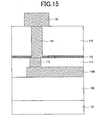
- Fig. 15 shows a structure to the left of the structure shown in Fig. 12, 13, or 14.
- a first wiring layer 110B is electrically connected to the source or drain of the MOS transistor (shown in Figs. 12 to 14).
- the steps before and including the step of depositing the silicon nitride film 123 to a thickness of 20 nm by a known CVD technique are the same as those described in connection with the third embodiment, a description of these steps is not provided herein.
- the silicon nitride film 123 shown in Fig. 15 corresponds to the sidewall protective film 123 (for the chalcogenide material layer) shown in Fig. 14.
- an interlayer insulating film 118 made up of a silicon oxide film is deposited on the entire surface, and its surface roughness is removed by a known CMP technique, planarizing the surface.
- a plug contact hole reaching the surface of the silicon nitride film 123 is formed by a lithographic process and a dry etching process.
- This dry etching process is performed under such conditions that the etching rate of the silicon oxide film is higher than that of the silicon nitride film.
- dry etching is further performed under such conditions that the etching rate of the silicon nitride film is higher than that of the silicon oxide film to extend the plug contact hole to the surfaces of the tungsten plug 112 and the interlayer insulating film 111.
- the interlayer insulating film 111 is not deeply etched.
- a tungsten layer is formed buried in the plug contact hole, and a tungsten plug 119 is formed by a known CMP technique.
- an aluminum layer is deposited to a thickness of 200 nm and processed to form a second wiring layer 120.
- copper which has lower resistance than aluminum, may be used instead of aluminum.
- a silicon nitride film is preferably used as the sidewall protective film for the chalcogenide material layer.
- first and second embodiments provide exemplary adhesive layers and the third embodiment provides an exemplary sidewall protective film, separately. However, these embodiments may be combined as necessary to collectively utilize their effects.
- the present invention can be applied to semiconductor integrated circuit devices that employ phase change memory cells formed of a phase change material such as chalcogenide.
Landscapes
- Engineering & Computer Science (AREA)
- Manufacturing & Machinery (AREA)
- Semiconductor Memories (AREA)
Applications Claiming Priority (2)
| Application Number | Priority Date | Filing Date | Title |
|---|---|---|---|
| JP2004144704 | 2004-05-14 | ||
| PCT/JP2005/008419 WO2005112118A1 (fr) | 2004-05-14 | 2005-05-09 | Mémoire de semi-conducteur |
Publications (3)
| Publication Number | Publication Date |
|---|---|
| EP1748488A1 true EP1748488A1 (fr) | 2007-01-31 |
| EP1748488A4 EP1748488A4 (fr) | 2010-04-07 |
| EP1748488B1 EP1748488B1 (fr) | 2012-08-29 |
Family
ID=35394429
Family Applications (1)
| Application Number | Title | Priority Date | Filing Date |
|---|---|---|---|
| EP05737197A Active EP1748488B1 (fr) | 2004-05-14 | 2005-05-09 | Mémoire de semi-conducteur |
Country Status (7)
| Country | Link |
|---|---|
| US (6) | US20070170413A1 (fr) |
| EP (1) | EP1748488B1 (fr) |
| JP (2) | JP5281746B2 (fr) |
| KR (1) | KR101029339B1 (fr) |
| CN (2) | CN101834198A (fr) |
| TW (2) | TWI487093B (fr) |
| WO (1) | WO2005112118A1 (fr) |
Cited By (4)
| Publication number | Priority date | Publication date | Assignee | Title |
|---|---|---|---|---|
| WO2007053474A2 (fr) * | 2005-10-28 | 2007-05-10 | Intel Corporation | Augmentation de la marge de pose d'une colonne de memoire a changement de phase |
| DE102007035857A1 (de) * | 2007-07-31 | 2009-02-05 | Qimonda Ag | Verfahren zum Herstellen einer Speichervorrichtung, Speichervorrichtung, Zelle, integrierte Schaltung, Speichermodul und Computersystem |
| WO2010008938A1 (fr) * | 2008-07-15 | 2010-01-21 | Sandisk 3D, Llc | Dispositifs électroniques comprenant des films à base de carbone pourvus de revêtements de paroi latérale, et procédé de fabrication de tels dispositifs |
| US8270205B2 (en) | 2007-05-25 | 2012-09-18 | Micron Technology, Inc. | Variable resistance memory device with an interfacial adhesion heating layer, systems using the same and methods forming the same |
Families Citing this family (43)
| Publication number | Priority date | Publication date | Assignee | Title |
|---|---|---|---|---|
| JP5281746B2 (ja) * | 2004-05-14 | 2013-09-04 | ルネサスエレクトロニクス株式会社 | 半導体記憶装置 |
| JP2006352082A (ja) * | 2005-05-19 | 2006-12-28 | Renesas Technology Corp | 半導体記憶装置及びその製造方法 |
| JP2007165710A (ja) * | 2005-12-15 | 2007-06-28 | Elpida Memory Inc | 不揮発性メモリ素子の製造方法 |
| KR100718156B1 (ko) * | 2006-02-27 | 2007-05-14 | 삼성전자주식회사 | 상전이 메모리 소자 및 그 제조방법 |
| US7324365B2 (en) * | 2006-03-02 | 2008-01-29 | Infineon Technologies Ag | Phase change memory fabricated using self-aligned processing |
| US8395199B2 (en) * | 2006-03-25 | 2013-03-12 | 4D-S Pty Ltd. | Systems and methods for fabricating self-aligned memory cell |
| US20070249116A1 (en) * | 2006-04-19 | 2007-10-25 | Philipp Jan B | Transitioning the state of phase change material by annealing |
| US7414883B2 (en) * | 2006-04-20 | 2008-08-19 | Intel Corporation | Programming a normally single phase chalcogenide material for use as a memory or FPLA |
| KR101038611B1 (ko) * | 2006-05-31 | 2011-06-03 | 르네사스 일렉트로닉스 가부시키가이샤 | 반도체 장치 |
| US20110049454A1 (en) * | 2006-06-23 | 2011-03-03 | Motoyasu Terao | Semiconductor device |
| WO2008001411A1 (fr) * | 2006-06-23 | 2008-01-03 | Renesas Technology Corp. | Procédé de production de dispositif mémoire à semi-conducteur |
| US7932548B2 (en) | 2006-07-14 | 2011-04-26 | 4D-S Pty Ltd. | Systems and methods for fabricating self-aligned memory cell |
| US8319204B2 (en) | 2006-07-21 | 2012-11-27 | Renesas Electronics Corporation | Semiconductor device |
| WO2008035392A1 (fr) * | 2006-09-19 | 2008-03-27 | Renesas Technology Corp. | Dispositif de circuit intégré à semi-conducteur |
| WO2008041285A1 (fr) * | 2006-09-29 | 2008-04-10 | Renesas Technology Corp. | Procédé de production d'un dispositif de mémoire à semi-conducteurs |
| KR100766499B1 (ko) * | 2006-10-20 | 2007-10-15 | 삼성전자주식회사 | 상변화 기억 소자 및 그 형성 방법 |
| KR101131137B1 (ko) * | 2006-11-30 | 2012-04-03 | 삼성전자주식회사 | 확산 방지막을 포함하는 상변화 메모리 소자 및 그제조방법 |
| KR20080057094A (ko) * | 2006-12-19 | 2008-06-24 | 삼성전자주식회사 | 상변화 메모리 소자와 그 제조 및 동작 방법 |
| US20080253165A1 (en) * | 2007-04-10 | 2008-10-16 | Philippe Blanchard | Method of Manufacturing a Memory Device, Memory Device, Cell, Integrated Circuit, Memory Module, and Computing System |
| US20080314738A1 (en) | 2007-06-19 | 2008-12-25 | International Business Machines Corporation | Electrolytic Device Based on a Solution-Processed Electrolyte |
| KR100891523B1 (ko) | 2007-07-20 | 2009-04-06 | 주식회사 하이닉스반도체 | 상변화 기억 소자 |
| EP2207216B1 (fr) * | 2007-10-02 | 2014-07-09 | Ulvac, Inc. | Film de chalcogénure et son procédé de fabrication |
| KR101162760B1 (ko) * | 2007-10-08 | 2012-07-05 | 삼성전자주식회사 | 상변화 메모리 소자 및 그의 제조방법 |
| JP2009135219A (ja) | 2007-11-29 | 2009-06-18 | Renesas Technology Corp | 半導体装置およびその製造方法 |
| US7718990B2 (en) | 2007-12-04 | 2010-05-18 | Ovonyx, Inc. | Active material devices with containment layer |
| WO2009153870A1 (fr) * | 2008-06-18 | 2009-12-23 | キヤノンアネルバ株式会社 | Élément de mémoire à changement de phase, cellule de mémoire à changement de phase, dispositif de traitement sous vide, et procédé de fabrication d'élément de mémoire à changement de phase |
| US7888165B2 (en) | 2008-08-14 | 2011-02-15 | Micron Technology, Inc. | Methods of forming a phase change material |
| US7834342B2 (en) * | 2008-09-04 | 2010-11-16 | Micron Technology, Inc. | Phase change material and methods of forming the phase change material |
| US8891298B2 (en) | 2011-07-19 | 2014-11-18 | Greenthread, Llc | Lifetime mixed level non-volatile memory system |
| KR101046228B1 (ko) * | 2008-12-26 | 2011-07-04 | 주식회사 하이닉스반도체 | 상변화 메모리 소자 및 그 제조방법 |
| WO2010079827A1 (fr) * | 2009-01-09 | 2010-07-15 | 日本電気株式会社 | Dispositif semi-conducteur et son procédé de fabrication |
| US8344343B2 (en) * | 2009-04-01 | 2013-01-01 | Taiwan Semiconductor Manufacturing Company, Ltd. | Composite film for phase change memory devices |
| JP2011199215A (ja) * | 2010-03-24 | 2011-10-06 | Hitachi Ltd | 半導体記憶装置 |
| TWI469408B (zh) * | 2012-05-07 | 2015-01-11 | Univ Feng Chia | 超薄與多層結構相變化記憶體元件 |
| JP6201151B2 (ja) * | 2013-03-18 | 2017-09-27 | パナソニックIpマネジメント株式会社 | 不揮発性記憶装置及びその製造方法 |
| US9397143B2 (en) * | 2013-12-20 | 2016-07-19 | Intel Corporation | Liner for phase change memory (PCM) array and associated techniques and configurations |
| KR102029905B1 (ko) * | 2014-02-28 | 2019-10-08 | 에스케이하이닉스 주식회사 | 전자장치 및 그 제조방법 |
| US10622555B2 (en) | 2018-07-31 | 2020-04-14 | Taiwan Semiconductor Manufacturing Co., Ltd. | Film scheme to improve peeling in chalcogenide based PCRAM |
| KR102634805B1 (ko) * | 2018-08-23 | 2024-02-08 | 에스케이하이닉스 주식회사 | 전자 장치 및 그 제조 방법 |
| JP2020047743A (ja) | 2018-09-18 | 2020-03-26 | キオクシア株式会社 | 記憶装置 |
| US10720580B2 (en) * | 2018-10-22 | 2020-07-21 | Globalfoundries Singapore Pte. Ltd. | RRAM device and method of fabrication thereof |
| KR20210041692A (ko) | 2019-10-07 | 2021-04-16 | 삼성전자주식회사 | 가변 저항 메모리 소자 |
| CN111725397A (zh) * | 2020-01-19 | 2020-09-29 | 中国科学院上海微系统与信息技术研究所 | 一种相变材料结构、存储器单元及其制作方法 |
Citations (3)
| Publication number | Priority date | Publication date | Assignee | Title |
|---|---|---|---|---|
| US20020080647A1 (en) * | 2000-12-21 | 2002-06-27 | Chien Chiang | Metal structure for a phase-change memory device |
| US20030001242A1 (en) * | 2001-06-30 | 2003-01-02 | Lowrey Tyler A. | Adhesive material for programmable device |
| EP1318552A1 (fr) * | 2001-12-05 | 2003-06-11 | STMicroelectronics S.r.l. | Région de contact à faible surface, élément de mémoire à changement de phase à efficience élevée et sa procédé de fabrication |
Family Cites Families (38)
| Publication number | Priority date | Publication date | Assignee | Title |
|---|---|---|---|---|
| JPH0445584A (ja) * | 1990-06-13 | 1992-02-14 | Casio Comput Co Ltd | 相転移型メモリ素子およびその製造方法 |
| US5869843A (en) * | 1995-06-07 | 1999-02-09 | Micron Technology, Inc. | Memory array having a multi-state element and method for forming such array or cells thereof |
| US5714768A (en) * | 1995-10-24 | 1998-02-03 | Energy Conversion Devices, Inc. | Second-layer phase change memory array on top of a logic device |
| US5998244A (en) * | 1996-08-22 | 1999-12-07 | Micron Technology, Inc. | Memory cell incorporating a chalcogenide element and method of making same |
| US5933365A (en) * | 1997-06-19 | 1999-08-03 | Energy Conversion Devices, Inc. | Memory element with energy control mechanism |
| JP2000004001A (ja) | 1998-06-15 | 2000-01-07 | Toshiba Corp | 半導体記憶装置及びその製造方法 |
| US7173317B1 (en) * | 1998-11-09 | 2007-02-06 | Micron Technology, Inc. | Electrical and thermal contact for use in semiconductor devices |
| WO2000057498A1 (fr) * | 1999-03-25 | 2000-09-28 | Energy Conversion Devices, Inc. | Element de memoire programmable electriquement muni de contacts ameliores |
| JP5646798B2 (ja) | 1999-11-11 | 2014-12-24 | ピーエスフォー ルクスコ エスエイアールエルPS4 Luxco S.a.r.l. | 半導体集積回路装置の製造方法 |
| US20020075631A1 (en) * | 1999-12-30 | 2002-06-20 | Applied Materials, Inc. | Iridium and iridium oxide electrodes used in ferroelectric capacitors |
| KR100372644B1 (ko) * | 2000-06-30 | 2003-02-17 | 주식회사 하이닉스반도체 | 비 휘발성 반도체 메모리 소자의 캐패시터 제조방법 |
| TW497327B (en) * | 2000-07-27 | 2002-08-01 | Wonderland Internat Inc | Simple flyback synchronous rectifier power supply |
| JP4470297B2 (ja) | 2000-08-14 | 2010-06-02 | ソニー株式会社 | 半導体装置の製造方法 |
| US6518671B1 (en) | 2000-10-30 | 2003-02-11 | Samsung Electronics Co. Ltd. | Bit line landing pad and borderless contact on bit line stud with localized etch stop layer and manufacturing method thereof |
| US6762090B2 (en) * | 2001-09-13 | 2004-07-13 | Hynix Semiconductor Inc. | Method for fabricating a capacitor |
| JP4911845B2 (ja) * | 2001-09-20 | 2012-04-04 | 株式会社リコー | 相変化型不揮発性メモリ素子、該相変化型不揮発性メモリ素子を用いたメモリアレーおよび該相変化型不揮発性メモリ素子の情報記録方法 |
| JP3749847B2 (ja) * | 2001-09-27 | 2006-03-01 | 株式会社東芝 | 相変化型不揮発性記憶装置及びその駆動回路 |
| US6815818B2 (en) * | 2001-11-19 | 2004-11-09 | Micron Technology, Inc. | Electrode structure for use in an integrated circuit |
| US6791859B2 (en) * | 2001-11-20 | 2004-09-14 | Micron Technology, Inc. | Complementary bit PCRAM sense amplifier and method of operation |
| EP1326254B1 (fr) * | 2001-12-27 | 2009-02-25 | STMicroelectronics S.r.l. | Architecture d'une mémoire non volatile de type changement de phase |
| JP3948292B2 (ja) * | 2002-02-01 | 2007-07-25 | 株式会社日立製作所 | 半導体記憶装置及びその製造方法 |
| US6891747B2 (en) * | 2002-02-20 | 2005-05-10 | Stmicroelectronics S.R.L. | Phase change memory cell and manufacturing method thereof using minitrenches |
| US6930913B2 (en) * | 2002-02-20 | 2005-08-16 | Stmicroelectronics S.R.L. | Contact structure, phase change memory cell, and manufacturing method thereof with elimination of double contacts |
| JP4103497B2 (ja) * | 2002-04-18 | 2008-06-18 | ソニー株式会社 | 記憶装置とその製造方法および使用方法、半導体装置とその製造方法 |
| US6583507B1 (en) * | 2002-04-26 | 2003-06-24 | Bum Ki Moon | Barrier for capacitor over plug structures |
| KR100437458B1 (ko) * | 2002-05-07 | 2004-06-23 | 삼성전자주식회사 | 상변화 기억 셀들 및 그 제조방법들 |
| US6872963B2 (en) * | 2002-08-08 | 2005-03-29 | Ovonyx, Inc. | Programmable resistance memory element with layered memory material |
| KR100448893B1 (ko) * | 2002-08-23 | 2004-09-16 | 삼성전자주식회사 | 상전이 기억 소자 구조 및 그 제조 방법 |
| JP2004096014A (ja) | 2002-09-03 | 2004-03-25 | Sharp Corp | 半導体不揮発性メモリセル、半導体不揮発性メモリ装置および半導体不揮発性メモリセルの製造方法 |
| JP3906139B2 (ja) * | 2002-10-16 | 2007-04-18 | 株式会社東芝 | 磁気ランダムアクセスメモリ |
| KR100481865B1 (ko) * | 2002-11-01 | 2005-04-11 | 삼성전자주식회사 | 상변환 기억소자 및 그 제조방법 |
| US6744088B1 (en) * | 2002-12-13 | 2004-06-01 | Intel Corporation | Phase change memory device on a planar composite layer |
| US7115927B2 (en) * | 2003-02-24 | 2006-10-03 | Samsung Electronics Co., Ltd. | Phase changeable memory devices |
| KR100560659B1 (ko) * | 2003-03-21 | 2006-03-16 | 삼성전자주식회사 | 상변화 기억 소자 및 그 제조 방법 |
| JP4254293B2 (ja) * | 2003-03-25 | 2009-04-15 | 株式会社日立製作所 | 記憶装置 |
| DE60306893T2 (de) * | 2003-05-07 | 2007-02-01 | Stmicroelectronics S.R.L., Agrate Brianza | Verfahren zur Herstellung einer elektrischen Speichereinrichtung mit Auswahltransistoren für Speicherelemente sowie entsprechend hergestellte Speichereinrichtung |
| JP5281746B2 (ja) | 2004-05-14 | 2013-09-04 | ルネサスエレクトロニクス株式会社 | 半導体記憶装置 |
| US7411208B2 (en) * | 2004-05-27 | 2008-08-12 | Samsung Electronics Co., Ltd. | Phase-change memory device having a barrier layer and manufacturing method |
-
2005
- 2005-05-09 JP JP2006513531A patent/JP5281746B2/ja active Active
- 2005-05-09 KR KR1020067023717A patent/KR101029339B1/ko active IP Right Grant
- 2005-05-09 US US11/596,220 patent/US20070170413A1/en not_active Abandoned
- 2005-05-09 EP EP05737197A patent/EP1748488B1/fr active Active
- 2005-05-09 WO PCT/JP2005/008419 patent/WO2005112118A1/fr not_active Application Discontinuation
- 2005-05-09 CN CN201010162083A patent/CN101834198A/zh active Pending
- 2005-05-09 CN CN2005800153010A patent/CN1954428B/zh active Active
- 2005-05-13 TW TW100145624A patent/TWI487093B/zh active
- 2005-05-13 TW TW094115624A patent/TW200620632A/zh unknown
-
2009
- 2009-11-05 US US12/613,235 patent/US8890107B2/en active Active
-
2011
- 2011-10-03 JP JP2011218893A patent/JP5466681B2/ja active Active
- 2011-12-07 US US13/314,165 patent/US8866120B2/en active Active
- 2011-12-07 US US13/314,154 patent/US8859344B2/en active Active
-
2012
- 2012-06-11 US US13/493,442 patent/US20120241715A1/en not_active Abandoned
-
2015
- 2015-04-09 US US14/683,112 patent/US20150214476A1/en not_active Abandoned
Patent Citations (3)
| Publication number | Priority date | Publication date | Assignee | Title |
|---|---|---|---|---|
| US20020080647A1 (en) * | 2000-12-21 | 2002-06-27 | Chien Chiang | Metal structure for a phase-change memory device |
| US20030001242A1 (en) * | 2001-06-30 | 2003-01-02 | Lowrey Tyler A. | Adhesive material for programmable device |
| EP1318552A1 (fr) * | 2001-12-05 | 2003-06-11 | STMicroelectronics S.r.l. | Région de contact à faible surface, élément de mémoire à changement de phase à efficience élevée et sa procédé de fabrication |
Non-Patent Citations (1)
| Title |
|---|
| See also references of WO2005112118A1 * |
Cited By (8)
| Publication number | Priority date | Publication date | Assignee | Title |
|---|---|---|---|---|
| WO2007053474A2 (fr) * | 2005-10-28 | 2007-05-10 | Intel Corporation | Augmentation de la marge de pose d'une colonne de memoire a changement de phase |
| WO2007053474A3 (fr) * | 2005-10-28 | 2007-08-02 | Intel Corp | Augmentation de la marge de pose d'une colonne de memoire a changement de phase |
| US7390691B2 (en) | 2005-10-28 | 2008-06-24 | Intel Corporation | Increasing phase change memory column landing margin |
| US8270205B2 (en) | 2007-05-25 | 2012-09-18 | Micron Technology, Inc. | Variable resistance memory device with an interfacial adhesion heating layer, systems using the same and methods forming the same |
| US8717799B2 (en) | 2007-05-25 | 2014-05-06 | Micron Technology, Inc. | Variable resistance memory device with an interfacial adhesion heating layer, systems using the same and methods of forming the same |
| DE102007035857A1 (de) * | 2007-07-31 | 2009-02-05 | Qimonda Ag | Verfahren zum Herstellen einer Speichervorrichtung, Speichervorrichtung, Zelle, integrierte Schaltung, Speichermodul und Computersystem |
| WO2010008938A1 (fr) * | 2008-07-15 | 2010-01-21 | Sandisk 3D, Llc | Dispositifs électroniques comprenant des films à base de carbone pourvus de revêtements de paroi latérale, et procédé de fabrication de tels dispositifs |
| US8309407B2 (en) | 2008-07-15 | 2012-11-13 | Sandisk 3D Llc | Electronic devices including carbon-based films having sidewall liners, and methods of forming such devices |
Also Published As
| Publication number | Publication date |
|---|---|
| WO2005112118A1 (fr) | 2005-11-24 |
| US20100044672A1 (en) | 2010-02-25 |
| US20070170413A1 (en) | 2007-07-26 |
| US20120077325A1 (en) | 2012-03-29 |
| TW201222787A (en) | 2012-06-01 |
| US8866120B2 (en) | 2014-10-21 |
| CN1954428B (zh) | 2010-09-29 |
| EP1748488B1 (fr) | 2012-08-29 |
| JPWO2005112118A1 (ja) | 2008-03-27 |
| KR20070009702A (ko) | 2007-01-18 |
| US8859344B2 (en) | 2014-10-14 |
| US20120241715A1 (en) | 2012-09-27 |
| US20150214476A1 (en) | 2015-07-30 |
| JP5466681B2 (ja) | 2014-04-09 |
| CN101834198A (zh) | 2010-09-15 |
| EP1748488A4 (fr) | 2010-04-07 |
| TWI367561B (fr) | 2012-07-01 |
| CN1954428A (zh) | 2007-04-25 |
| US20120074377A1 (en) | 2012-03-29 |
| JP2012039134A (ja) | 2012-02-23 |
| JP5281746B2 (ja) | 2013-09-04 |
| KR101029339B1 (ko) | 2011-04-13 |
| TWI487093B (zh) | 2015-06-01 |
| TW200620632A (en) | 2006-06-16 |
| US8890107B2 (en) | 2014-11-18 |
Similar Documents
| Publication | Publication Date | Title |
|---|---|---|
| EP1748488B1 (fr) | Mémoire de semi-conducteur | |
| US6569705B2 (en) | Metal structure for a phase-change memory device | |
| US8023310B2 (en) | Nonvolatile memory cell including carbon storage element formed on a silicide layer | |
| US20090085023A1 (en) | Phase change memory structures | |
| US20070246748A1 (en) | Phase change memory cell with limited switchable volume | |
| JP2004119958A (ja) | 1t1r型抵抗メモリアレイを製造する方法 | |
| JP2006352082A (ja) | 半導体記憶装置及びその製造方法 | |
| JP5039035B2 (ja) | 半導体装置 | |
| CN102237390A (zh) | 半导体装置及其制造方法 | |
| US8097873B2 (en) | Phase change memory structures | |
| US20100096610A1 (en) | Phase-change material memory cell | |
| JP2006294970A (ja) | 半導体装置 | |
| US7994536B2 (en) | Integrated circuit including U-shaped access device | |
| JP2012064965A (ja) | 半導体装置及びその製造方法 |
Legal Events
| Date | Code | Title | Description |
|---|---|---|---|
| PUAI | Public reference made under article 153(3) epc to a published international application that has entered the european phase |
Free format text: ORIGINAL CODE: 0009012 |
|
| 17P | Request for examination filed |
Effective date: 20061214 |
|
| AK | Designated contracting states |
Kind code of ref document: A1 Designated state(s): DE FR NL |
|
| DAX | Request for extension of the european patent (deleted) | ||
| RBV | Designated contracting states (corrected) |
Designated state(s): DE FR NL |
|
| A4 | Supplementary search report drawn up and despatched |
Effective date: 20100310 |
|
| 17Q | First examination report despatched |
Effective date: 20100511 |
|
| RAP1 | Party data changed (applicant data changed or rights of an application transferred) |
Owner name: RENESAS ELECTRONICS CORPORATION |
|
| REG | Reference to a national code |
Ref country code: DE Ref legal event code: R079 Ref document number: 602005035888 Country of ref document: DE Free format text: PREVIOUS MAIN CLASS: H01L0027100000 Ipc: H01L0027240000 |
|
| GRAP | Despatch of communication of intention to grant a patent |
Free format text: ORIGINAL CODE: EPIDOSNIGR1 |
|
| RIC1 | Information provided on ipc code assigned before grant |
Ipc: H01L 27/24 20060101AFI20120314BHEP Ipc: H01L 45/00 20060101ALI20120314BHEP |
|
| RIN1 | Information on inventor provided before grant (corrected) |
Inventor name: TAKAURA, NAOKI Inventor name: IWASAKI, TOMIO Inventor name: MATSUI, YUICHI Inventor name: MATSUZAKI, NOZOMU Inventor name: YAMAMOTO, NAOKI Inventor name: MATSUOKA, HIDEYUKI |
|
| GRAS | Grant fee paid |
Free format text: ORIGINAL CODE: EPIDOSNIGR3 |
|
| GRAA | (expected) grant |
Free format text: ORIGINAL CODE: 0009210 |
|
| RIN1 | Information on inventor provided before grant (corrected) |
Inventor name: MATSUZAKI, NOZOMU Inventor name: TAKAURA, NORIKATSU Inventor name: MATSUI, YUICHI Inventor name: IWASAKI, TOMIO Inventor name: YAMAMOTO, NAOKI Inventor name: MATSUOKA, HIDEYUKI |
|
| AK | Designated contracting states |
Kind code of ref document: B1 Designated state(s): DE FR NL |
|
| REG | Reference to a national code |
Ref country code: DE Ref legal event code: R081 Ref document number: 602005035888 Country of ref document: DE Owner name: RENESAS ELECTRONICS CORPORATION, JP Free format text: FORMER OWNER: RENESAS TECHNOLOGY CORP., TOKYO, JP |
|
| REG | Reference to a national code |
Ref country code: NL Ref legal event code: T3 |
|
| REG | Reference to a national code |
Ref country code: DE Ref legal event code: R096 Ref document number: 602005035888 Country of ref document: DE Effective date: 20121025 |
|
| PLBE | No opposition filed within time limit |
Free format text: ORIGINAL CODE: 0009261 |
|
| STAA | Information on the status of an ep patent application or granted ep patent |
Free format text: STATUS: NO OPPOSITION FILED WITHIN TIME LIMIT |
|
| 26N | No opposition filed |
Effective date: 20130530 |
|
| REG | Reference to a national code |
Ref country code: DE Ref legal event code: R097 Ref document number: 602005035888 Country of ref document: DE Effective date: 20130530 |
|
| REG | Reference to a national code |
Ref country code: FR Ref legal event code: PLFP Year of fee payment: 11 |
|
| PGFP | Annual fee paid to national office [announced via postgrant information from national office to epo] |
Ref country code: NL Payment date: 20150409 Year of fee payment: 11 Ref country code: FR Payment date: 20150508 Year of fee payment: 11 |
|
| REG | Reference to a national code |
Ref country code: NL Ref legal event code: MM Effective date: 20160601 |
|
| PG25 | Lapsed in a contracting state [announced via postgrant information from national office to epo] |
Ref country code: NL Free format text: LAPSE BECAUSE OF NON-PAYMENT OF DUE FEES Effective date: 20160601 |
|
| REG | Reference to a national code |
Ref country code: FR Ref legal event code: ST Effective date: 20170131 |
|
| PG25 | Lapsed in a contracting state [announced via postgrant information from national office to epo] |
Ref country code: FR Free format text: LAPSE BECAUSE OF NON-PAYMENT OF DUE FEES Effective date: 20160531 |
|
| REG | Reference to a national code |
Ref country code: DE Ref legal event code: R082 Ref document number: 602005035888 Country of ref document: DE Representative=s name: BEETZ & PARTNER MBB PATENTANWAELTE, DE Ref country code: DE Ref legal event code: R082 Ref document number: 602005035888 Country of ref document: DE Representative=s name: BEETZ & PARTNER MBB PATENT- UND RECHTSANWAELTE, DE Ref country code: DE Ref legal event code: R081 Ref document number: 602005035888 Country of ref document: DE Owner name: RENESAS ELECTRONICS CORPORATION, JP Free format text: FORMER OWNER: RENESAS ELECTRONICS CORP., KAWASAKI-SHI, KANAGAWA, JP |
|
| REG | Reference to a national code |
Ref country code: DE Ref legal event code: R079 Ref document number: 602005035888 Country of ref document: DE Free format text: PREVIOUS MAIN CLASS: H01L0027240000 Ipc: H10B0063000000 |
|
| PGFP | Annual fee paid to national office [announced via postgrant information from national office to epo] |
Ref country code: DE Payment date: 20230328 Year of fee payment: 19 |