EP1732116B1 - Methode zum Bonden mikroelektronischer Bauteile und damit hergestellte Vorrichtung - Google Patents
Methode zum Bonden mikroelektronischer Bauteile und damit hergestellte Vorrichtung Download PDFInfo
- Publication number
- EP1732116B1 EP1732116B1 EP06114933.2A EP06114933A EP1732116B1 EP 1732116 B1 EP1732116 B1 EP 1732116B1 EP 06114933 A EP06114933 A EP 06114933A EP 1732116 B1 EP1732116 B1 EP 1732116B1
- Authority
- EP
- European Patent Office
- Prior art keywords
- layer
- solder
- micropattern
- bonding
- metal
- Prior art date
- Legal status (The legal status is an assumption and is not a legal conclusion. Google has not performed a legal analysis and makes no representation as to the accuracy of the status listed.)
- Active
Links
- 238000000034 method Methods 0.000 title claims description 48
- 238000004377 microelectronic Methods 0.000 title description 3
- 229910000679 solder Inorganic materials 0.000 claims description 102
- 239000010410 layer Substances 0.000 claims description 94
- 239000002184 metal Substances 0.000 claims description 79
- 229910052751 metal Inorganic materials 0.000 claims description 79
- 239000000463 material Substances 0.000 claims description 60
- 229910052718 tin Inorganic materials 0.000 claims description 24
- 229920000642 polymer Polymers 0.000 claims description 23
- 239000012790 adhesive layer Substances 0.000 claims description 21
- 238000005304 joining Methods 0.000 claims description 8
- UMIVXZPTRXBADB-UHFFFAOYSA-N benzocyclobutene Chemical compound C1=CC=C2CCC2=C1 UMIVXZPTRXBADB-UHFFFAOYSA-N 0.000 claims description 7
- 229910017052 cobalt Inorganic materials 0.000 claims description 7
- 239000010941 cobalt Substances 0.000 claims description 7
- GUTLYIVDDKVIGB-UHFFFAOYSA-N cobalt atom Chemical compound [Co] GUTLYIVDDKVIGB-UHFFFAOYSA-N 0.000 claims description 7
- 229920001296 polysiloxane Polymers 0.000 claims description 5
- 239000000203 mixture Substances 0.000 claims description 3
- ATJFFYVFTNAWJD-UHFFFAOYSA-N Tin Chemical group [Sn] ATJFFYVFTNAWJD-UHFFFAOYSA-N 0.000 claims description 2
- 239000000758 substrate Substances 0.000 description 35
- 238000002844 melting Methods 0.000 description 27
- 229910000765 intermetallic Inorganic materials 0.000 description 26
- 239000003292 glue Substances 0.000 description 24
- 230000008018 melting Effects 0.000 description 20
- 235000012431 wafers Nutrition 0.000 description 20
- 150000002739 metals Chemical class 0.000 description 15
- 229910045601 alloy Inorganic materials 0.000 description 13
- 239000000956 alloy Substances 0.000 description 13
- 239000010949 copper Substances 0.000 description 12
- 239000000853 adhesive Substances 0.000 description 9
- 230000001070 adhesive effect Effects 0.000 description 9
- 229910019043 CoSn Inorganic materials 0.000 description 8
- 229910019050 CoSn2 Inorganic materials 0.000 description 8
- 230000008569 process Effects 0.000 description 8
- 238000000059 patterning Methods 0.000 description 6
- 238000006243 chemical reaction Methods 0.000 description 5
- 229910052802 copper Inorganic materials 0.000 description 5
- 238000009792 diffusion process Methods 0.000 description 5
- CFAKWWQIUFSQFU-UHFFFAOYSA-N 2-hydroxy-3-methylcyclopent-2-en-1-one Chemical compound CC1=C(O)C(=O)CC1 CFAKWWQIUFSQFU-UHFFFAOYSA-N 0.000 description 4
- IJGRMHOSHXDMSA-UHFFFAOYSA-N Atomic nitrogen Chemical compound N#N IJGRMHOSHXDMSA-UHFFFAOYSA-N 0.000 description 4
- 229910020646 Co-Sn Inorganic materials 0.000 description 4
- 229910020709 Co—Sn Inorganic materials 0.000 description 4
- PXHVJJICTQNCMI-UHFFFAOYSA-N Nickel Chemical compound [Ni] PXHVJJICTQNCMI-UHFFFAOYSA-N 0.000 description 4
- 238000000137 annealing Methods 0.000 description 4
- 239000000155 melt Substances 0.000 description 4
- 230000001590 oxidative effect Effects 0.000 description 4
- RYGMFSIKBFXOCR-UHFFFAOYSA-N Copper Chemical compound [Cu] RYGMFSIKBFXOCR-UHFFFAOYSA-N 0.000 description 3
- 230000008901 benefit Effects 0.000 description 3
- 230000003993 interaction Effects 0.000 description 3
- 238000003475 lamination Methods 0.000 description 3
- 238000001465 metallisation Methods 0.000 description 3
- 230000003647 oxidation Effects 0.000 description 3
- 238000007254 oxidation reaction Methods 0.000 description 3
- 239000013047 polymeric layer Substances 0.000 description 3
- 238000005476 soldering Methods 0.000 description 3
- 238000004528 spin coating Methods 0.000 description 3
- 238000005507 spraying Methods 0.000 description 3
- 238000009736 wetting Methods 0.000 description 3
- 239000001837 2-hydroxy-3-methylcyclopent-2-en-1-one Substances 0.000 description 2
- 229910017755 Cu-Sn Inorganic materials 0.000 description 2
- 229910017927 Cu—Sn Inorganic materials 0.000 description 2
- 239000000654 additive Substances 0.000 description 2
- 238000001816 cooling Methods 0.000 description 2
- KUNSUQLRTQLHQQ-UHFFFAOYSA-N copper tin Chemical compound [Cu].[Sn] KUNSUQLRTQLHQQ-UHFFFAOYSA-N 0.000 description 2
- 238000011161 development Methods 0.000 description 2
- 238000009713 electroplating Methods 0.000 description 2
- 230000008020 evaporation Effects 0.000 description 2
- 238000001704 evaporation Methods 0.000 description 2
- 239000007789 gas Substances 0.000 description 2
- 229910052738 indium Inorganic materials 0.000 description 2
- 239000001995 intermetallic alloy Substances 0.000 description 2
- 239000007788 liquid Substances 0.000 description 2
- 238000004519 manufacturing process Methods 0.000 description 2
- 229910052759 nickel Inorganic materials 0.000 description 2
- 229910052757 nitrogen Inorganic materials 0.000 description 2
- 238000010943 off-gassing Methods 0.000 description 2
- 238000002161 passivation Methods 0.000 description 2
- 238000007711 solidification Methods 0.000 description 2
- 230000008023 solidification Effects 0.000 description 2
- 239000000126 substance Substances 0.000 description 2
- 230000007704 transition Effects 0.000 description 2
- 229910016347 CuSn Inorganic materials 0.000 description 1
- 238000013459 approach Methods 0.000 description 1
- 230000000712 assembly Effects 0.000 description 1
- 238000000429 assembly Methods 0.000 description 1
- 230000004888 barrier function Effects 0.000 description 1
- 230000015572 biosynthetic process Effects 0.000 description 1
- 238000004364 calculation method Methods 0.000 description 1
- 230000000295 complement effect Effects 0.000 description 1
- 239000002131 composite material Substances 0.000 description 1
- 238000007766 curtain coating Methods 0.000 description 1
- 230000001351 cycling effect Effects 0.000 description 1
- 238000005516 engineering process Methods 0.000 description 1
- 229910052737 gold Inorganic materials 0.000 description 1
- 230000036541 health Effects 0.000 description 1
- 238000004806 packaging method and process Methods 0.000 description 1
- 238000007747 plating Methods 0.000 description 1
- 238000002360 preparation method Methods 0.000 description 1
- 238000012545 processing Methods 0.000 description 1
- 239000007787 solid Substances 0.000 description 1
- 238000009987 spinning Methods 0.000 description 1
- 238000012360 testing method Methods 0.000 description 1
- 230000000930 thermomechanical effect Effects 0.000 description 1
Images


Classifications
-
- H—ELECTRICITY
- H01—ELECTRIC ELEMENTS
- H01L—SEMICONDUCTOR DEVICES NOT COVERED BY CLASS H10
- H01L24/00—Arrangements for connecting or disconnecting semiconductor or solid-state bodies; Methods or apparatus related thereto
- H01L24/01—Means for bonding being attached to, or being formed on, the surface to be connected, e.g. chip-to-package, die-attach, "first-level" interconnects; Manufacturing methods related thereto
- H01L24/10—Bump connectors ; Manufacturing methods related thereto
- H01L24/11—Manufacturing methods
-
- B—PERFORMING OPERATIONS; TRANSPORTING
- B81—MICROSTRUCTURAL TECHNOLOGY
- B81C—PROCESSES OR APPARATUS SPECIALLY ADAPTED FOR THE MANUFACTURE OR TREATMENT OF MICROSTRUCTURAL DEVICES OR SYSTEMS
- B81C1/00—Manufacture or treatment of devices or systems in or on a substrate
- B81C1/00015—Manufacture or treatment of devices or systems in or on a substrate for manufacturing microsystems
- B81C1/00261—Processes for packaging MEMS devices
- B81C1/00333—Aspects relating to packaging of MEMS devices, not covered by groups B81C1/00269 - B81C1/00325
-
- H—ELECTRICITY
- H01—ELECTRIC ELEMENTS
- H01L—SEMICONDUCTOR DEVICES NOT COVERED BY CLASS H10
- H01L21/00—Processes or apparatus adapted for the manufacture or treatment of semiconductor or solid state devices or of parts thereof
- H01L21/02—Manufacture or treatment of semiconductor devices or of parts thereof
- H01L21/04—Manufacture or treatment of semiconductor devices or of parts thereof the devices having at least one potential-jump barrier or surface barrier, e.g. PN junction, depletion layer or carrier concentration layer
- H01L21/48—Manufacture or treatment of parts, e.g. containers, prior to assembly of the devices, using processes not provided for in a single one of the subgroups H01L21/06 - H01L21/326
- H01L21/4814—Conductive parts
- H01L21/4846—Leads on or in insulating or insulated substrates, e.g. metallisation
-
- H—ELECTRICITY
- H01—ELECTRIC ELEMENTS
- H01L—SEMICONDUCTOR DEVICES NOT COVERED BY CLASS H10
- H01L21/00—Processes or apparatus adapted for the manufacture or treatment of semiconductor or solid state devices or of parts thereof
- H01L21/02—Manufacture or treatment of semiconductor devices or of parts thereof
- H01L21/04—Manufacture or treatment of semiconductor devices or of parts thereof the devices having at least one potential-jump barrier or surface barrier, e.g. PN junction, depletion layer or carrier concentration layer
- H01L21/50—Assembly of semiconductor devices using processes or apparatus not provided for in a single one of the subgroups H01L21/06 - H01L21/326, e.g. sealing of a cap to a base of a container
- H01L21/56—Encapsulations, e.g. encapsulation layers, coatings
- H01L21/563—Encapsulation of active face of flip-chip device, e.g. underfilling or underencapsulation of flip-chip, encapsulation preform on chip or mounting substrate
-
- H—ELECTRICITY
- H01—ELECTRIC ELEMENTS
- H01L—SEMICONDUCTOR DEVICES NOT COVERED BY CLASS H10
- H01L24/00—Arrangements for connecting or disconnecting semiconductor or solid-state bodies; Methods or apparatus related thereto
- H01L24/01—Means for bonding being attached to, or being formed on, the surface to be connected, e.g. chip-to-package, die-attach, "first-level" interconnects; Manufacturing methods related thereto
- H01L24/10—Bump connectors ; Manufacturing methods related thereto
- H01L24/12—Structure, shape, material or disposition of the bump connectors prior to the connecting process
- H01L24/13—Structure, shape, material or disposition of the bump connectors prior to the connecting process of an individual bump connector
-
- H—ELECTRICITY
- H01—ELECTRIC ELEMENTS
- H01L—SEMICONDUCTOR DEVICES NOT COVERED BY CLASS H10
- H01L24/00—Arrangements for connecting or disconnecting semiconductor or solid-state bodies; Methods or apparatus related thereto
- H01L24/01—Means for bonding being attached to, or being formed on, the surface to be connected, e.g. chip-to-package, die-attach, "first-level" interconnects; Manufacturing methods related thereto
- H01L24/26—Layer connectors, e.g. plate connectors, solder or adhesive layers; Manufacturing methods related thereto
- H01L24/28—Structure, shape, material or disposition of the layer connectors prior to the connecting process
- H01L24/29—Structure, shape, material or disposition of the layer connectors prior to the connecting process of an individual layer connector
-
- H—ELECTRICITY
- H01—ELECTRIC ELEMENTS
- H01L—SEMICONDUCTOR DEVICES NOT COVERED BY CLASS H10
- H01L24/00—Arrangements for connecting or disconnecting semiconductor or solid-state bodies; Methods or apparatus related thereto
- H01L24/80—Methods for connecting semiconductor or other solid state bodies using means for bonding being attached to, or being formed on, the surface to be connected
- H01L24/81—Methods for connecting semiconductor or other solid state bodies using means for bonding being attached to, or being formed on, the surface to be connected using a bump connector
-
- H—ELECTRICITY
- H01—ELECTRIC ELEMENTS
- H01L—SEMICONDUCTOR DEVICES NOT COVERED BY CLASS H10
- H01L24/00—Arrangements for connecting or disconnecting semiconductor or solid-state bodies; Methods or apparatus related thereto
- H01L24/93—Batch processes
- H01L24/95—Batch processes at chip-level, i.e. with connecting carried out on a plurality of singulated devices, i.e. on diced chips
- H01L24/97—Batch processes at chip-level, i.e. with connecting carried out on a plurality of singulated devices, i.e. on diced chips the devices being connected to a common substrate, e.g. interposer, said common substrate being separable into individual assemblies after connecting
-
- H—ELECTRICITY
- H01—ELECTRIC ELEMENTS
- H01L—SEMICONDUCTOR DEVICES NOT COVERED BY CLASS H10
- H01L25/00—Assemblies consisting of a plurality of individual semiconductor or other solid state devices ; Multistep manufacturing processes thereof
- H01L25/50—Multistep manufacturing processes of assemblies consisting of devices, each device being of a type provided for in group H01L27/00 or H01L29/00
-
- H—ELECTRICITY
- H01—ELECTRIC ELEMENTS
- H01L—SEMICONDUCTOR DEVICES NOT COVERED BY CLASS H10
- H01L2224/00—Indexing scheme for arrangements for connecting or disconnecting semiconductor or solid-state bodies and methods related thereto as covered by H01L24/00
- H01L2224/01—Means for bonding being attached to, or being formed on, the surface to be connected, e.g. chip-to-package, die-attach, "first-level" interconnects; Manufacturing methods related thereto
- H01L2224/02—Bonding areas; Manufacturing methods related thereto
- H01L2224/04—Structure, shape, material or disposition of the bonding areas prior to the connecting process
- H01L2224/05—Structure, shape, material or disposition of the bonding areas prior to the connecting process of an individual bonding area
- H01L2224/05001—Internal layers
- H01L2224/0502—Disposition
- H01L2224/05022—Disposition the internal layer being at least partially embedded in the surface
-
- H—ELECTRICITY
- H01—ELECTRIC ELEMENTS
- H01L—SEMICONDUCTOR DEVICES NOT COVERED BY CLASS H10
- H01L2224/00—Indexing scheme for arrangements for connecting or disconnecting semiconductor or solid-state bodies and methods related thereto as covered by H01L24/00
- H01L2224/01—Means for bonding being attached to, or being formed on, the surface to be connected, e.g. chip-to-package, die-attach, "first-level" interconnects; Manufacturing methods related thereto
- H01L2224/02—Bonding areas; Manufacturing methods related thereto
- H01L2224/04—Structure, shape, material or disposition of the bonding areas prior to the connecting process
- H01L2224/05—Structure, shape, material or disposition of the bonding areas prior to the connecting process of an individual bonding area
- H01L2224/05001—Internal layers
- H01L2224/05099—Material
- H01L2224/051—Material with a principal constituent of the material being a metal or a metalloid, e.g. boron [B], silicon [Si], germanium [Ge], arsenic [As], antimony [Sb], tellurium [Te] and polonium [Po], and alloys thereof
- H01L2224/05138—Material with a principal constituent of the material being a metal or a metalloid, e.g. boron [B], silicon [Si], germanium [Ge], arsenic [As], antimony [Sb], tellurium [Te] and polonium [Po], and alloys thereof the principal constituent melting at a temperature of greater than or equal to 950°C and less than 1550°C
- H01L2224/05147—Copper [Cu] as principal constituent
-
- H—ELECTRICITY
- H01—ELECTRIC ELEMENTS
- H01L—SEMICONDUCTOR DEVICES NOT COVERED BY CLASS H10
- H01L2224/00—Indexing scheme for arrangements for connecting or disconnecting semiconductor or solid-state bodies and methods related thereto as covered by H01L24/00
- H01L2224/01—Means for bonding being attached to, or being formed on, the surface to be connected, e.g. chip-to-package, die-attach, "first-level" interconnects; Manufacturing methods related thereto
- H01L2224/02—Bonding areas; Manufacturing methods related thereto
- H01L2224/04—Structure, shape, material or disposition of the bonding areas prior to the connecting process
- H01L2224/05—Structure, shape, material or disposition of the bonding areas prior to the connecting process of an individual bonding area
- H01L2224/0554—External layer
- H01L2224/0556—Disposition
- H01L2224/0557—Disposition the external layer being disposed on a via connection of the semiconductor or solid-state body
-
- H—ELECTRICITY
- H01—ELECTRIC ELEMENTS
- H01L—SEMICONDUCTOR DEVICES NOT COVERED BY CLASS H10
- H01L2224/00—Indexing scheme for arrangements for connecting or disconnecting semiconductor or solid-state bodies and methods related thereto as covered by H01L24/00
- H01L2224/01—Means for bonding being attached to, or being formed on, the surface to be connected, e.g. chip-to-package, die-attach, "first-level" interconnects; Manufacturing methods related thereto
- H01L2224/02—Bonding areas; Manufacturing methods related thereto
- H01L2224/04—Structure, shape, material or disposition of the bonding areas prior to the connecting process
- H01L2224/05—Structure, shape, material or disposition of the bonding areas prior to the connecting process of an individual bonding area
- H01L2224/0554—External layer
- H01L2224/0556—Disposition
- H01L2224/05571—Disposition the external layer being disposed in a recess of the surface
-
- H—ELECTRICITY
- H01—ELECTRIC ELEMENTS
- H01L—SEMICONDUCTOR DEVICES NOT COVERED BY CLASS H10
- H01L2224/00—Indexing scheme for arrangements for connecting or disconnecting semiconductor or solid-state bodies and methods related thereto as covered by H01L24/00
- H01L2224/01—Means for bonding being attached to, or being formed on, the surface to be connected, e.g. chip-to-package, die-attach, "first-level" interconnects; Manufacturing methods related thereto
- H01L2224/02—Bonding areas; Manufacturing methods related thereto
- H01L2224/04—Structure, shape, material or disposition of the bonding areas prior to the connecting process
- H01L2224/05—Structure, shape, material or disposition of the bonding areas prior to the connecting process of an individual bonding area
- H01L2224/0554—External layer
- H01L2224/05599—Material
- H01L2224/056—Material with a principal constituent of the material being a metal or a metalloid, e.g. boron [B], silicon [Si], germanium [Ge], arsenic [As], antimony [Sb], tellurium [Te] and polonium [Po], and alloys thereof
- H01L2224/05638—Material with a principal constituent of the material being a metal or a metalloid, e.g. boron [B], silicon [Si], germanium [Ge], arsenic [As], antimony [Sb], tellurium [Te] and polonium [Po], and alloys thereof the principal constituent melting at a temperature of greater than or equal to 950°C and less than 1550°C
- H01L2224/05647—Copper [Cu] as principal constituent
-
- H—ELECTRICITY
- H01—ELECTRIC ELEMENTS
- H01L—SEMICONDUCTOR DEVICES NOT COVERED BY CLASS H10
- H01L2224/00—Indexing scheme for arrangements for connecting or disconnecting semiconductor or solid-state bodies and methods related thereto as covered by H01L24/00
- H01L2224/01—Means for bonding being attached to, or being formed on, the surface to be connected, e.g. chip-to-package, die-attach, "first-level" interconnects; Manufacturing methods related thereto
- H01L2224/10—Bump connectors; Manufacturing methods related thereto
- H01L2224/1012—Auxiliary members for bump connectors, e.g. spacers
- H01L2224/10122—Auxiliary members for bump connectors, e.g. spacers being formed on the semiconductor or solid-state body to be connected
- H01L2224/10135—Alignment aids
-
- H—ELECTRICITY
- H01—ELECTRIC ELEMENTS
- H01L—SEMICONDUCTOR DEVICES NOT COVERED BY CLASS H10
- H01L2224/00—Indexing scheme for arrangements for connecting or disconnecting semiconductor or solid-state bodies and methods related thereto as covered by H01L24/00
- H01L2224/01—Means for bonding being attached to, or being formed on, the surface to be connected, e.g. chip-to-package, die-attach, "first-level" interconnects; Manufacturing methods related thereto
- H01L2224/10—Bump connectors; Manufacturing methods related thereto
- H01L2224/1012—Auxiliary members for bump connectors, e.g. spacers
- H01L2224/10152—Auxiliary members for bump connectors, e.g. spacers being formed on an item to be connected not being a semiconductor or solid-state body
- H01L2224/10165—Alignment aids
-
- H—ELECTRICITY
- H01—ELECTRIC ELEMENTS
- H01L—SEMICONDUCTOR DEVICES NOT COVERED BY CLASS H10
- H01L2224/00—Indexing scheme for arrangements for connecting or disconnecting semiconductor or solid-state bodies and methods related thereto as covered by H01L24/00
- H01L2224/01—Means for bonding being attached to, or being formed on, the surface to be connected, e.g. chip-to-package, die-attach, "first-level" interconnects; Manufacturing methods related thereto
- H01L2224/10—Bump connectors; Manufacturing methods related thereto
- H01L2224/11—Manufacturing methods
- H01L2224/1147—Manufacturing methods using a lift-off mask
-
- H—ELECTRICITY
- H01—ELECTRIC ELEMENTS
- H01L—SEMICONDUCTOR DEVICES NOT COVERED BY CLASS H10
- H01L2224/00—Indexing scheme for arrangements for connecting or disconnecting semiconductor or solid-state bodies and methods related thereto as covered by H01L24/00
- H01L2224/01—Means for bonding being attached to, or being formed on, the surface to be connected, e.g. chip-to-package, die-attach, "first-level" interconnects; Manufacturing methods related thereto
- H01L2224/10—Bump connectors; Manufacturing methods related thereto
- H01L2224/12—Structure, shape, material or disposition of the bump connectors prior to the connecting process
- H01L2224/13—Structure, shape, material or disposition of the bump connectors prior to the connecting process of an individual bump connector
- H01L2224/13001—Core members of the bump connector
- H01L2224/13075—Plural core members
- H01L2224/1308—Plural core members being stacked
- H01L2224/13082—Two-layer arrangements
-
- H—ELECTRICITY
- H01—ELECTRIC ELEMENTS
- H01L—SEMICONDUCTOR DEVICES NOT COVERED BY CLASS H10
- H01L2224/00—Indexing scheme for arrangements for connecting or disconnecting semiconductor or solid-state bodies and methods related thereto as covered by H01L24/00
- H01L2224/01—Means for bonding being attached to, or being formed on, the surface to be connected, e.g. chip-to-package, die-attach, "first-level" interconnects; Manufacturing methods related thereto
- H01L2224/10—Bump connectors; Manufacturing methods related thereto
- H01L2224/12—Structure, shape, material or disposition of the bump connectors prior to the connecting process
- H01L2224/13—Structure, shape, material or disposition of the bump connectors prior to the connecting process of an individual bump connector
- H01L2224/13001—Core members of the bump connector
- H01L2224/13099—Material
- H01L2224/131—Material with a principal constituent of the material being a metal or a metalloid, e.g. boron [B], silicon [Si], germanium [Ge], arsenic [As], antimony [Sb], tellurium [Te] and polonium [Po], and alloys thereof
- H01L2224/13101—Material with a principal constituent of the material being a metal or a metalloid, e.g. boron [B], silicon [Si], germanium [Ge], arsenic [As], antimony [Sb], tellurium [Te] and polonium [Po], and alloys thereof the principal constituent melting at a temperature of less than 400°C
- H01L2224/13109—Indium [In] as principal constituent
-
- H—ELECTRICITY
- H01—ELECTRIC ELEMENTS
- H01L—SEMICONDUCTOR DEVICES NOT COVERED BY CLASS H10
- H01L2224/00—Indexing scheme for arrangements for connecting or disconnecting semiconductor or solid-state bodies and methods related thereto as covered by H01L24/00
- H01L2224/01—Means for bonding being attached to, or being formed on, the surface to be connected, e.g. chip-to-package, die-attach, "first-level" interconnects; Manufacturing methods related thereto
- H01L2224/10—Bump connectors; Manufacturing methods related thereto
- H01L2224/12—Structure, shape, material or disposition of the bump connectors prior to the connecting process
- H01L2224/13—Structure, shape, material or disposition of the bump connectors prior to the connecting process of an individual bump connector
- H01L2224/13001—Core members of the bump connector
- H01L2224/13099—Material
- H01L2224/131—Material with a principal constituent of the material being a metal or a metalloid, e.g. boron [B], silicon [Si], germanium [Ge], arsenic [As], antimony [Sb], tellurium [Te] and polonium [Po], and alloys thereof
- H01L2224/13101—Material with a principal constituent of the material being a metal or a metalloid, e.g. boron [B], silicon [Si], germanium [Ge], arsenic [As], antimony [Sb], tellurium [Te] and polonium [Po], and alloys thereof the principal constituent melting at a temperature of less than 400°C
- H01L2224/13111—Tin [Sn] as principal constituent
-
- H—ELECTRICITY
- H01—ELECTRIC ELEMENTS
- H01L—SEMICONDUCTOR DEVICES NOT COVERED BY CLASS H10
- H01L2224/00—Indexing scheme for arrangements for connecting or disconnecting semiconductor or solid-state bodies and methods related thereto as covered by H01L24/00
- H01L2224/01—Means for bonding being attached to, or being formed on, the surface to be connected, e.g. chip-to-package, die-attach, "first-level" interconnects; Manufacturing methods related thereto
- H01L2224/10—Bump connectors; Manufacturing methods related thereto
- H01L2224/12—Structure, shape, material or disposition of the bump connectors prior to the connecting process
- H01L2224/13—Structure, shape, material or disposition of the bump connectors prior to the connecting process of an individual bump connector
- H01L2224/13001—Core members of the bump connector
- H01L2224/13099—Material
- H01L2224/131—Material with a principal constituent of the material being a metal or a metalloid, e.g. boron [B], silicon [Si], germanium [Ge], arsenic [As], antimony [Sb], tellurium [Te] and polonium [Po], and alloys thereof
- H01L2224/13138—Material with a principal constituent of the material being a metal or a metalloid, e.g. boron [B], silicon [Si], germanium [Ge], arsenic [As], antimony [Sb], tellurium [Te] and polonium [Po], and alloys thereof the principal constituent melting at a temperature of greater than or equal to 950°C and less than 1550°C
- H01L2224/13144—Gold [Au] as principal constituent
-
- H—ELECTRICITY
- H01—ELECTRIC ELEMENTS
- H01L—SEMICONDUCTOR DEVICES NOT COVERED BY CLASS H10
- H01L2224/00—Indexing scheme for arrangements for connecting or disconnecting semiconductor or solid-state bodies and methods related thereto as covered by H01L24/00
- H01L2224/01—Means for bonding being attached to, or being formed on, the surface to be connected, e.g. chip-to-package, die-attach, "first-level" interconnects; Manufacturing methods related thereto
- H01L2224/10—Bump connectors; Manufacturing methods related thereto
- H01L2224/12—Structure, shape, material or disposition of the bump connectors prior to the connecting process
- H01L2224/13—Structure, shape, material or disposition of the bump connectors prior to the connecting process of an individual bump connector
- H01L2224/13001—Core members of the bump connector
- H01L2224/13099—Material
- H01L2224/131—Material with a principal constituent of the material being a metal or a metalloid, e.g. boron [B], silicon [Si], germanium [Ge], arsenic [As], antimony [Sb], tellurium [Te] and polonium [Po], and alloys thereof
- H01L2224/13138—Material with a principal constituent of the material being a metal or a metalloid, e.g. boron [B], silicon [Si], germanium [Ge], arsenic [As], antimony [Sb], tellurium [Te] and polonium [Po], and alloys thereof the principal constituent melting at a temperature of greater than or equal to 950°C and less than 1550°C
- H01L2224/13147—Copper [Cu] as principal constituent
-
- H—ELECTRICITY
- H01—ELECTRIC ELEMENTS
- H01L—SEMICONDUCTOR DEVICES NOT COVERED BY CLASS H10
- H01L2224/00—Indexing scheme for arrangements for connecting or disconnecting semiconductor or solid-state bodies and methods related thereto as covered by H01L24/00
- H01L2224/01—Means for bonding being attached to, or being formed on, the surface to be connected, e.g. chip-to-package, die-attach, "first-level" interconnects; Manufacturing methods related thereto
- H01L2224/10—Bump connectors; Manufacturing methods related thereto
- H01L2224/12—Structure, shape, material or disposition of the bump connectors prior to the connecting process
- H01L2224/13—Structure, shape, material or disposition of the bump connectors prior to the connecting process of an individual bump connector
- H01L2224/13001—Core members of the bump connector
- H01L2224/13099—Material
- H01L2224/131—Material with a principal constituent of the material being a metal or a metalloid, e.g. boron [B], silicon [Si], germanium [Ge], arsenic [As], antimony [Sb], tellurium [Te] and polonium [Po], and alloys thereof
- H01L2224/13138—Material with a principal constituent of the material being a metal or a metalloid, e.g. boron [B], silicon [Si], germanium [Ge], arsenic [As], antimony [Sb], tellurium [Te] and polonium [Po], and alloys thereof the principal constituent melting at a temperature of greater than or equal to 950°C and less than 1550°C
- H01L2224/13157—Cobalt [Co] as principal constituent
-
- H—ELECTRICITY
- H01—ELECTRIC ELEMENTS
- H01L—SEMICONDUCTOR DEVICES NOT COVERED BY CLASS H10
- H01L2224/00—Indexing scheme for arrangements for connecting or disconnecting semiconductor or solid-state bodies and methods related thereto as covered by H01L24/00
- H01L2224/01—Means for bonding being attached to, or being formed on, the surface to be connected, e.g. chip-to-package, die-attach, "first-level" interconnects; Manufacturing methods related thereto
- H01L2224/10—Bump connectors; Manufacturing methods related thereto
- H01L2224/12—Structure, shape, material or disposition of the bump connectors prior to the connecting process
- H01L2224/13—Structure, shape, material or disposition of the bump connectors prior to the connecting process of an individual bump connector
- H01L2224/1354—Coating
- H01L2224/13599—Material
- H01L2224/136—Material with a principal constituent of the material being a metal or a metalloid, e.g. boron [B], silicon [Si], germanium [Ge], arsenic [As], antimony [Sb], tellurium [Te] and polonium [Po], and alloys thereof
- H01L2224/13601—Material with a principal constituent of the material being a metal or a metalloid, e.g. boron [B], silicon [Si], germanium [Ge], arsenic [As], antimony [Sb], tellurium [Te] and polonium [Po], and alloys thereof the principal constituent melting at a temperature of less than 400°C
- H01L2224/13609—Indium [In] as principal constituent
-
- H—ELECTRICITY
- H01—ELECTRIC ELEMENTS
- H01L—SEMICONDUCTOR DEVICES NOT COVERED BY CLASS H10
- H01L2224/00—Indexing scheme for arrangements for connecting or disconnecting semiconductor or solid-state bodies and methods related thereto as covered by H01L24/00
- H01L2224/01—Means for bonding being attached to, or being formed on, the surface to be connected, e.g. chip-to-package, die-attach, "first-level" interconnects; Manufacturing methods related thereto
- H01L2224/10—Bump connectors; Manufacturing methods related thereto
- H01L2224/15—Structure, shape, material or disposition of the bump connectors after the connecting process
- H01L2224/16—Structure, shape, material or disposition of the bump connectors after the connecting process of an individual bump connector
- H01L2224/161—Disposition
- H01L2224/16135—Disposition the bump connector connecting between different semiconductor or solid-state bodies, i.e. chip-to-chip
- H01L2224/16145—Disposition the bump connector connecting between different semiconductor or solid-state bodies, i.e. chip-to-chip the bodies being stacked
-
- H—ELECTRICITY
- H01—ELECTRIC ELEMENTS
- H01L—SEMICONDUCTOR DEVICES NOT COVERED BY CLASS H10
- H01L2224/00—Indexing scheme for arrangements for connecting or disconnecting semiconductor or solid-state bodies and methods related thereto as covered by H01L24/00
- H01L2224/01—Means for bonding being attached to, or being formed on, the surface to be connected, e.g. chip-to-package, die-attach, "first-level" interconnects; Manufacturing methods related thereto
- H01L2224/26—Layer connectors, e.g. plate connectors, solder or adhesive layers; Manufacturing methods related thereto
- H01L2224/28—Structure, shape, material or disposition of the layer connectors prior to the connecting process
- H01L2224/29—Structure, shape, material or disposition of the layer connectors prior to the connecting process of an individual layer connector
- H01L2224/29001—Core members of the layer connector
- H01L2224/29099—Material
- H01L2224/291—Material with a principal constituent of the material being a metal or a metalloid, e.g. boron [B], silicon [Si], germanium [Ge], arsenic [As], antimony [Sb], tellurium [Te] and polonium [Po], and alloys thereof
- H01L2224/29101—Material with a principal constituent of the material being a metal or a metalloid, e.g. boron [B], silicon [Si], germanium [Ge], arsenic [As], antimony [Sb], tellurium [Te] and polonium [Po], and alloys thereof the principal constituent melting at a temperature of less than 400°C
- H01L2224/29111—Tin [Sn] as principal constituent
-
- H—ELECTRICITY
- H01—ELECTRIC ELEMENTS
- H01L—SEMICONDUCTOR DEVICES NOT COVERED BY CLASS H10
- H01L2224/00—Indexing scheme for arrangements for connecting or disconnecting semiconductor or solid-state bodies and methods related thereto as covered by H01L24/00
- H01L2224/73—Means for bonding being of different types provided for in two or more of groups H01L2224/10, H01L2224/18, H01L2224/26, H01L2224/34, H01L2224/42, H01L2224/50, H01L2224/63, H01L2224/71
- H01L2224/732—Location after the connecting process
- H01L2224/73201—Location after the connecting process on the same surface
- H01L2224/73203—Bump and layer connectors
-
- H—ELECTRICITY
- H01—ELECTRIC ELEMENTS
- H01L—SEMICONDUCTOR DEVICES NOT COVERED BY CLASS H10
- H01L2224/00—Indexing scheme for arrangements for connecting or disconnecting semiconductor or solid-state bodies and methods related thereto as covered by H01L24/00
- H01L2224/80—Methods for connecting semiconductor or other solid state bodies using means for bonding being attached to, or being formed on, the surface to be connected
- H01L2224/81—Methods for connecting semiconductor or other solid state bodies using means for bonding being attached to, or being formed on, the surface to be connected using a bump connector
- H01L2224/8112—Aligning
- H01L2224/81136—Aligning involving guiding structures, e.g. spacers or supporting members
- H01L2224/81138—Aligning involving guiding structures, e.g. spacers or supporting members the guiding structures being at least partially left in the finished device
- H01L2224/81139—Guiding structures on the body
-
- H—ELECTRICITY
- H01—ELECTRIC ELEMENTS
- H01L—SEMICONDUCTOR DEVICES NOT COVERED BY CLASS H10
- H01L2224/00—Indexing scheme for arrangements for connecting or disconnecting semiconductor or solid-state bodies and methods related thereto as covered by H01L24/00
- H01L2224/80—Methods for connecting semiconductor or other solid state bodies using means for bonding being attached to, or being formed on, the surface to be connected
- H01L2224/81—Methods for connecting semiconductor or other solid state bodies using means for bonding being attached to, or being formed on, the surface to be connected using a bump connector
- H01L2224/8112—Aligning
- H01L2224/81136—Aligning involving guiding structures, e.g. spacers or supporting members
- H01L2224/81138—Aligning involving guiding structures, e.g. spacers or supporting members the guiding structures being at least partially left in the finished device
- H01L2224/8114—Guiding structures outside the body
-
- H—ELECTRICITY
- H01—ELECTRIC ELEMENTS
- H01L—SEMICONDUCTOR DEVICES NOT COVERED BY CLASS H10
- H01L2224/00—Indexing scheme for arrangements for connecting or disconnecting semiconductor or solid-state bodies and methods related thereto as covered by H01L24/00
- H01L2224/80—Methods for connecting semiconductor or other solid state bodies using means for bonding being attached to, or being formed on, the surface to be connected
- H01L2224/81—Methods for connecting semiconductor or other solid state bodies using means for bonding being attached to, or being formed on, the surface to be connected using a bump connector
- H01L2224/8119—Arrangement of the bump connectors prior to mounting
- H01L2224/81191—Arrangement of the bump connectors prior to mounting wherein the bump connectors are disposed only on the semiconductor or solid-state body
-
- H—ELECTRICITY
- H01—ELECTRIC ELEMENTS
- H01L—SEMICONDUCTOR DEVICES NOT COVERED BY CLASS H10
- H01L2224/00—Indexing scheme for arrangements for connecting or disconnecting semiconductor or solid-state bodies and methods related thereto as covered by H01L24/00
- H01L2224/80—Methods for connecting semiconductor or other solid state bodies using means for bonding being attached to, or being formed on, the surface to be connected
- H01L2224/81—Methods for connecting semiconductor or other solid state bodies using means for bonding being attached to, or being formed on, the surface to be connected using a bump connector
- H01L2224/8119—Arrangement of the bump connectors prior to mounting
- H01L2224/81192—Arrangement of the bump connectors prior to mounting wherein the bump connectors are disposed only on another item or body to be connected to the semiconductor or solid-state body
-
- H—ELECTRICITY
- H01—ELECTRIC ELEMENTS
- H01L—SEMICONDUCTOR DEVICES NOT COVERED BY CLASS H10
- H01L2224/00—Indexing scheme for arrangements for connecting or disconnecting semiconductor or solid-state bodies and methods related thereto as covered by H01L24/00
- H01L2224/80—Methods for connecting semiconductor or other solid state bodies using means for bonding being attached to, or being formed on, the surface to be connected
- H01L2224/81—Methods for connecting semiconductor or other solid state bodies using means for bonding being attached to, or being formed on, the surface to be connected using a bump connector
- H01L2224/812—Applying energy for connecting
- H01L2224/81201—Compression bonding
- H01L2224/81203—Thermocompression bonding, e.g. diffusion bonding, pressure joining, thermocompression welding or solid-state welding
-
- H—ELECTRICITY
- H01—ELECTRIC ELEMENTS
- H01L—SEMICONDUCTOR DEVICES NOT COVERED BY CLASS H10
- H01L2224/00—Indexing scheme for arrangements for connecting or disconnecting semiconductor or solid-state bodies and methods related thereto as covered by H01L24/00
- H01L2224/80—Methods for connecting semiconductor or other solid state bodies using means for bonding being attached to, or being formed on, the surface to be connected
- H01L2224/81—Methods for connecting semiconductor or other solid state bodies using means for bonding being attached to, or being formed on, the surface to be connected using a bump connector
- H01L2224/812—Applying energy for connecting
- H01L2224/8121—Applying energy for connecting using a reflow oven
-
- H—ELECTRICITY
- H01—ELECTRIC ELEMENTS
- H01L—SEMICONDUCTOR DEVICES NOT COVERED BY CLASS H10
- H01L2224/00—Indexing scheme for arrangements for connecting or disconnecting semiconductor or solid-state bodies and methods related thereto as covered by H01L24/00
- H01L2224/80—Methods for connecting semiconductor or other solid state bodies using means for bonding being attached to, or being formed on, the surface to be connected
- H01L2224/81—Methods for connecting semiconductor or other solid state bodies using means for bonding being attached to, or being formed on, the surface to be connected using a bump connector
- H01L2224/818—Bonding techniques
- H01L2224/81801—Soldering or alloying
- H01L2224/8181—Soldering or alloying involving forming an intermetallic compound at the bonding interface
-
- H—ELECTRICITY
- H01—ELECTRIC ELEMENTS
- H01L—SEMICONDUCTOR DEVICES NOT COVERED BY CLASS H10
- H01L2224/00—Indexing scheme for arrangements for connecting or disconnecting semiconductor or solid-state bodies and methods related thereto as covered by H01L24/00
- H01L2224/80—Methods for connecting semiconductor or other solid state bodies using means for bonding being attached to, or being formed on, the surface to be connected
- H01L2224/81—Methods for connecting semiconductor or other solid state bodies using means for bonding being attached to, or being formed on, the surface to be connected using a bump connector
- H01L2224/818—Bonding techniques
- H01L2224/81801—Soldering or alloying
- H01L2224/81815—Reflow soldering
-
- H—ELECTRICITY
- H01—ELECTRIC ELEMENTS
- H01L—SEMICONDUCTOR DEVICES NOT COVERED BY CLASS H10
- H01L2224/00—Indexing scheme for arrangements for connecting or disconnecting semiconductor or solid-state bodies and methods related thereto as covered by H01L24/00
- H01L2224/80—Methods for connecting semiconductor or other solid state bodies using means for bonding being attached to, or being formed on, the surface to be connected
- H01L2224/81—Methods for connecting semiconductor or other solid state bodies using means for bonding being attached to, or being formed on, the surface to be connected using a bump connector
- H01L2224/818—Bonding techniques
- H01L2224/81801—Soldering or alloying
- H01L2224/8182—Diffusion bonding
- H01L2224/81825—Solid-liquid interdiffusion
-
- H—ELECTRICITY
- H01—ELECTRIC ELEMENTS
- H01L—SEMICONDUCTOR DEVICES NOT COVERED BY CLASS H10
- H01L2224/00—Indexing scheme for arrangements for connecting or disconnecting semiconductor or solid-state bodies and methods related thereto as covered by H01L24/00
- H01L2224/80—Methods for connecting semiconductor or other solid state bodies using means for bonding being attached to, or being formed on, the surface to be connected
- H01L2224/81—Methods for connecting semiconductor or other solid state bodies using means for bonding being attached to, or being formed on, the surface to be connected using a bump connector
- H01L2224/818—Bonding techniques
- H01L2224/81801—Soldering or alloying
- H01L2224/8182—Diffusion bonding
- H01L2224/8183—Solid-solid interdiffusion
-
- H—ELECTRICITY
- H01—ELECTRIC ELEMENTS
- H01L—SEMICONDUCTOR DEVICES NOT COVERED BY CLASS H10
- H01L2224/00—Indexing scheme for arrangements for connecting or disconnecting semiconductor or solid-state bodies and methods related thereto as covered by H01L24/00
- H01L2224/80—Methods for connecting semiconductor or other solid state bodies using means for bonding being attached to, or being formed on, the surface to be connected
- H01L2224/81—Methods for connecting semiconductor or other solid state bodies using means for bonding being attached to, or being formed on, the surface to be connected using a bump connector
- H01L2224/81905—Combinations of bonding methods provided for in at least two different groups from H01L2224/818 - H01L2224/81904
- H01L2224/81907—Intermediate bonding, i.e. intermediate bonding step for temporarily bonding the semiconductor or solid-state body, followed by at least a further bonding step
-
- H—ELECTRICITY
- H01—ELECTRIC ELEMENTS
- H01L—SEMICONDUCTOR DEVICES NOT COVERED BY CLASS H10
- H01L2224/00—Indexing scheme for arrangements for connecting or disconnecting semiconductor or solid-state bodies and methods related thereto as covered by H01L24/00
- H01L2224/80—Methods for connecting semiconductor or other solid state bodies using means for bonding being attached to, or being formed on, the surface to be connected
- H01L2224/81—Methods for connecting semiconductor or other solid state bodies using means for bonding being attached to, or being formed on, the surface to be connected using a bump connector
- H01L2224/81909—Post-treatment of the bump connector or bonding area
- H01L2224/81948—Thermal treatments, e.g. annealing, controlled cooling
-
- H—ELECTRICITY
- H01—ELECTRIC ELEMENTS
- H01L—SEMICONDUCTOR DEVICES NOT COVERED BY CLASS H10
- H01L2224/00—Indexing scheme for arrangements for connecting or disconnecting semiconductor or solid-state bodies and methods related thereto as covered by H01L24/00
- H01L2224/80—Methods for connecting semiconductor or other solid state bodies using means for bonding being attached to, or being formed on, the surface to be connected
- H01L2224/83—Methods for connecting semiconductor or other solid state bodies using means for bonding being attached to, or being formed on, the surface to be connected using a layer connector
- H01L2224/8319—Arrangement of the layer connectors prior to mounting
- H01L2224/83191—Arrangement of the layer connectors prior to mounting wherein the layer connectors are disposed only on the semiconductor or solid-state body
-
- H—ELECTRICITY
- H01—ELECTRIC ELEMENTS
- H01L—SEMICONDUCTOR DEVICES NOT COVERED BY CLASS H10
- H01L2224/00—Indexing scheme for arrangements for connecting or disconnecting semiconductor or solid-state bodies and methods related thereto as covered by H01L24/00
- H01L2224/80—Methods for connecting semiconductor or other solid state bodies using means for bonding being attached to, or being formed on, the surface to be connected
- H01L2224/83—Methods for connecting semiconductor or other solid state bodies using means for bonding being attached to, or being formed on, the surface to be connected using a layer connector
- H01L2224/8319—Arrangement of the layer connectors prior to mounting
- H01L2224/83192—Arrangement of the layer connectors prior to mounting wherein the layer connectors are disposed only on another item or body to be connected to the semiconductor or solid-state body
-
- H—ELECTRICITY
- H01—ELECTRIC ELEMENTS
- H01L—SEMICONDUCTOR DEVICES NOT COVERED BY CLASS H10
- H01L2224/00—Indexing scheme for arrangements for connecting or disconnecting semiconductor or solid-state bodies and methods related thereto as covered by H01L24/00
- H01L2224/80—Methods for connecting semiconductor or other solid state bodies using means for bonding being attached to, or being formed on, the surface to be connected
- H01L2224/83—Methods for connecting semiconductor or other solid state bodies using means for bonding being attached to, or being formed on, the surface to be connected using a layer connector
- H01L2224/8319—Arrangement of the layer connectors prior to mounting
- H01L2224/83193—Arrangement of the layer connectors prior to mounting wherein the layer connectors are disposed on both the semiconductor or solid-state body and another item or body to be connected to the semiconductor or solid-state body
-
- H—ELECTRICITY
- H01—ELECTRIC ELEMENTS
- H01L—SEMICONDUCTOR DEVICES NOT COVERED BY CLASS H10
- H01L2224/00—Indexing scheme for arrangements for connecting or disconnecting semiconductor or solid-state bodies and methods related thereto as covered by H01L24/00
- H01L2224/80—Methods for connecting semiconductor or other solid state bodies using means for bonding being attached to, or being formed on, the surface to be connected
- H01L2224/83—Methods for connecting semiconductor or other solid state bodies using means for bonding being attached to, or being formed on, the surface to be connected using a layer connector
- H01L2224/8319—Arrangement of the layer connectors prior to mounting
- H01L2224/83194—Lateral distribution of the layer connectors
-
- H—ELECTRICITY
- H01—ELECTRIC ELEMENTS
- H01L—SEMICONDUCTOR DEVICES NOT COVERED BY CLASS H10
- H01L2224/00—Indexing scheme for arrangements for connecting or disconnecting semiconductor or solid-state bodies and methods related thereto as covered by H01L24/00
- H01L2224/91—Methods for connecting semiconductor or solid state bodies including different methods provided for in two or more of groups H01L2224/80 - H01L2224/90
- H01L2224/92—Specific sequence of method steps
- H01L2224/921—Connecting a surface with connectors of different types
- H01L2224/9211—Parallel connecting processes
-
- H—ELECTRICITY
- H01—ELECTRIC ELEMENTS
- H01L—SEMICONDUCTOR DEVICES NOT COVERED BY CLASS H10
- H01L2224/00—Indexing scheme for arrangements for connecting or disconnecting semiconductor or solid-state bodies and methods related thereto as covered by H01L24/00
- H01L2224/93—Batch processes
- H01L2224/95—Batch processes at chip-level, i.e. with connecting carried out on a plurality of singulated devices, i.e. on diced chips
- H01L2224/97—Batch processes at chip-level, i.e. with connecting carried out on a plurality of singulated devices, i.e. on diced chips the devices being connected to a common substrate, e.g. interposer, said common substrate being separable into individual assemblies after connecting
-
- H—ELECTRICITY
- H01—ELECTRIC ELEMENTS
- H01L—SEMICONDUCTOR DEVICES NOT COVERED BY CLASS H10
- H01L2225/00—Details relating to assemblies covered by the group H01L25/00 but not provided for in its subgroups
- H01L2225/03—All the devices being of a type provided for in the same subgroup of groups H01L27/00 - H01L33/648 and H10K99/00
- H01L2225/04—All the devices being of a type provided for in the same subgroup of groups H01L27/00 - H01L33/648 and H10K99/00 the devices not having separate containers
- H01L2225/065—All the devices being of a type provided for in the same subgroup of groups H01L27/00 - H01L33/648 and H10K99/00 the devices not having separate containers the devices being of a type provided for in group H01L27/00
- H01L2225/06503—Stacked arrangements of devices
- H01L2225/06513—Bump or bump-like direct electrical connections between devices, e.g. flip-chip connection, solder bumps
-
- H—ELECTRICITY
- H01—ELECTRIC ELEMENTS
- H01L—SEMICONDUCTOR DEVICES NOT COVERED BY CLASS H10
- H01L2924/00—Indexing scheme for arrangements or methods for connecting or disconnecting semiconductor or solid-state bodies as covered by H01L24/00
- H01L2924/0001—Technical content checked by a classifier
- H01L2924/00013—Fully indexed content
-
- H—ELECTRICITY
- H01—ELECTRIC ELEMENTS
- H01L—SEMICONDUCTOR DEVICES NOT COVERED BY CLASS H10
- H01L2924/00—Indexing scheme for arrangements or methods for connecting or disconnecting semiconductor or solid-state bodies as covered by H01L24/00
- H01L2924/01—Chemical elements
- H01L2924/01005—Boron [B]
-
- H—ELECTRICITY
- H01—ELECTRIC ELEMENTS
- H01L—SEMICONDUCTOR DEVICES NOT COVERED BY CLASS H10
- H01L2924/00—Indexing scheme for arrangements or methods for connecting or disconnecting semiconductor or solid-state bodies as covered by H01L24/00
- H01L2924/01—Chemical elements
- H01L2924/01006—Carbon [C]
-
- H—ELECTRICITY
- H01—ELECTRIC ELEMENTS
- H01L—SEMICONDUCTOR DEVICES NOT COVERED BY CLASS H10
- H01L2924/00—Indexing scheme for arrangements or methods for connecting or disconnecting semiconductor or solid-state bodies as covered by H01L24/00
- H01L2924/01—Chemical elements
- H01L2924/01027—Cobalt [Co]
-
- H—ELECTRICITY
- H01—ELECTRIC ELEMENTS
- H01L—SEMICONDUCTOR DEVICES NOT COVERED BY CLASS H10
- H01L2924/00—Indexing scheme for arrangements or methods for connecting or disconnecting semiconductor or solid-state bodies as covered by H01L24/00
- H01L2924/01—Chemical elements
- H01L2924/01029—Copper [Cu]
-
- H—ELECTRICITY
- H01—ELECTRIC ELEMENTS
- H01L—SEMICONDUCTOR DEVICES NOT COVERED BY CLASS H10
- H01L2924/00—Indexing scheme for arrangements or methods for connecting or disconnecting semiconductor or solid-state bodies as covered by H01L24/00
- H01L2924/01—Chemical elements
- H01L2924/01033—Arsenic [As]
-
- H—ELECTRICITY
- H01—ELECTRIC ELEMENTS
- H01L—SEMICONDUCTOR DEVICES NOT COVERED BY CLASS H10
- H01L2924/00—Indexing scheme for arrangements or methods for connecting or disconnecting semiconductor or solid-state bodies as covered by H01L24/00
- H01L2924/01—Chemical elements
- H01L2924/0105—Tin [Sn]
-
- H—ELECTRICITY
- H01—ELECTRIC ELEMENTS
- H01L—SEMICONDUCTOR DEVICES NOT COVERED BY CLASS H10
- H01L2924/00—Indexing scheme for arrangements or methods for connecting or disconnecting semiconductor or solid-state bodies as covered by H01L24/00
- H01L2924/01—Chemical elements
- H01L2924/01079—Gold [Au]
-
- H—ELECTRICITY
- H01—ELECTRIC ELEMENTS
- H01L—SEMICONDUCTOR DEVICES NOT COVERED BY CLASS H10
- H01L2924/00—Indexing scheme for arrangements or methods for connecting or disconnecting semiconductor or solid-state bodies as covered by H01L24/00
- H01L2924/01—Chemical elements
- H01L2924/01082—Lead [Pb]
-
- H—ELECTRICITY
- H01—ELECTRIC ELEMENTS
- H01L—SEMICONDUCTOR DEVICES NOT COVERED BY CLASS H10
- H01L2924/00—Indexing scheme for arrangements or methods for connecting or disconnecting semiconductor or solid-state bodies as covered by H01L24/00
- H01L2924/013—Alloys
- H01L2924/0132—Binary Alloys
-
- H—ELECTRICITY
- H01—ELECTRIC ELEMENTS
- H01L—SEMICONDUCTOR DEVICES NOT COVERED BY CLASS H10
- H01L2924/00—Indexing scheme for arrangements or methods for connecting or disconnecting semiconductor or solid-state bodies as covered by H01L24/00
- H01L2924/013—Alloys
- H01L2924/0132—Binary Alloys
- H01L2924/01327—Intermediate phases, i.e. intermetallics compounds
-
- H—ELECTRICITY
- H01—ELECTRIC ELEMENTS
- H01L—SEMICONDUCTOR DEVICES NOT COVERED BY CLASS H10
- H01L2924/00—Indexing scheme for arrangements or methods for connecting or disconnecting semiconductor or solid-state bodies as covered by H01L24/00
- H01L2924/013—Alloys
- H01L2924/014—Solder alloys
-
- H—ELECTRICITY
- H01—ELECTRIC ELEMENTS
- H01L—SEMICONDUCTOR DEVICES NOT COVERED BY CLASS H10
- H01L2924/00—Indexing scheme for arrangements or methods for connecting or disconnecting semiconductor or solid-state bodies as covered by H01L24/00
- H01L2924/06—Polymers
- H01L2924/078—Adhesive characteristics other than chemical
- H01L2924/07802—Adhesive characteristics other than chemical not being an ohmic electrical conductor
-
- H—ELECTRICITY
- H01—ELECTRIC ELEMENTS
- H01L—SEMICONDUCTOR DEVICES NOT COVERED BY CLASS H10
- H01L2924/00—Indexing scheme for arrangements or methods for connecting or disconnecting semiconductor or solid-state bodies as covered by H01L24/00
- H01L2924/10—Details of semiconductor or other solid state devices to be connected
- H01L2924/11—Device type
- H01L2924/14—Integrated circuits
-
- H—ELECTRICITY
- H01—ELECTRIC ELEMENTS
- H01L—SEMICONDUCTOR DEVICES NOT COVERED BY CLASS H10
- H01L2924/00—Indexing scheme for arrangements or methods for connecting or disconnecting semiconductor or solid-state bodies as covered by H01L24/00
- H01L2924/10—Details of semiconductor or other solid state devices to be connected
- H01L2924/146—Mixed devices
- H01L2924/1461—MEMS
Definitions
- the present invention is related to the field of microelectronics. It relates to the fields of flip chip assembly, 3D-IC (3-dimensional Integrated Circuit) stacking, and MEMS packaging.
- chip-to-chip also referred to as die-to-die
- chip to wafer also referred to as die to wafer
- wafer to wafer bonding assemblies are critical because of: the small diameter and narrow spacing of the solder patterns which:
- Document EP1306897 discloses a a bonding method according to the preamble of claim 1.
- Document US20040096592 is related to an electroless cobalt plating solution, usable in combination with tin solder balls in the production of microelectronic devices.
- the cobalt serves as a barrier against copper diffusion.
- the present invention aims to provide a method for bonding 2 elements, as for instance chip-to-chip (also referred to as die-to-die), chip to wafer (also referred to as die to wafer, a wafer is also often called a substrate) or wafer to wafer bonding, which alleviates or avoids the problems of the prior art.
- chip-to-chip also referred to as die-to-die
- chip to wafer also referred to as die to wafer
- a wafer is also often called a substrate
- wafer to wafer bonding which alleviates or avoids the problems of the prior art.
- the invention is related to a method and devices such as described in the appended claims.
- One aspect of the present invention is similar to flip chip interconnect, but uses a low temperature melting metal or alloy and realizes an intermetallic connection.
- joined micropatterns may be used rather then solder balls : they have relatively small dimensions; they can be preferably thinner than 100 ⁇ m, more preferably thinner than 40 ⁇ m thick, or thinner then 20 ⁇ m, more preferably between 5 and 20 ⁇ m thick.
- a connection is preferably made by a thermo/compression-reflow method. This is a method where both pressure and heat are applied. Pressure establishes a first mechanical bond and heat causes a diffusion process which results in a metallic bond. When applied simultaneously, the thermal diffusion process can be accelerated due to the pressure.
- the connection could also be made by heat alone or by pressure alone, in appropriate circumstances.
- the entire solder volume is transformed into an intermetallic compound.
- Having a thin connection can be advantageous, since it allows for small thickness variation across the die and bonding substrates, which is reducing stress buildup and improves bonding-yield (can be smaller then solder thickness/2).
- a microsoldering method based on a Co/Sn system for the micropatterns is used. This has an additional and superior performance over the currently used/proposed solder alloys:
- a known way to reduce interfacial stresses, caused by differences in stiffness between different parts of the solder joint, is the application of an underfill after bonding, but void-free underfill of micro-pattern connected elements with traditional capillary underfill methods is very difficult, as the gap between the different die becomes too small.
- this gap is typically smaller then 40 microns, or smaller then 20 microns, or smaller then 10 microns, or smaller then 5 microns, or smaller then 1 micron.
- some connections may break even before application of such underfill.
- This type of underfill is moreover applied typically after having singulated the dies, which brings some degree of complexity.
- a pre-defined photo-patterned non-conductive glue layer or adhesive layer is applied around the micropatterns described in the previously mentioned embodiments.
- the non-conductive glue layer or adhesive (polymer 'underfill') and conductive micro-patterns can be applied in one single process flow.
- the electrical connections and adhesive joining can be performed in a common bonding process between two elements (eg. 2 substrates, 2 dies, or die and substrate, or other devices & substrates).
- the embodiments of the present invention may become the micro-pattern solution of choice in the future. Some of the parameters which may be considered when comparing different solutions can be scalability, process complexity, yield, current carrying capability and overall reliability.
- a method of bonding of two elements comprising
- a further annealing step is performed after the joining step. This further annealing step can be needed to ensure that all the remaining solder material is consumed to form intermetallics. This is to prevent the presence of a thin solder layer that would be the weakest point of the micropattern.
- the bonding strength of the permanent bond is preferably equal to or larger than the strength of a standard solder bump connection. Preferably it is higher then 6kgf/mm 2 .
- the first metal is the same as said second metal.
- the first micropattern and/or second micropattern comprise(s) further an upper layer which is a thin layer which can prevent oxidation of the first and second metal layers respectively, and/or which improves the wetting of the solder material to the first metal layer and/or second metal layer, and which dissolves or doesn't interfere in the interaction between the solder material and the first or second metal layer.
- a micropattern is a layered planar pattern with a thickness from a few 0.01 microns towards about 100 microns. It comprises at least one layer.
- the micropatterns can have any shape, and can be microbumps, which have a localised nature.
- the microbumps have an essentially circular, rectangular or square shape with a diameter smaller then 10 microns, or 1 micron.
- the micropatterns can have any appropriate structure, as for instance a closed structure e.g. a ring or rectangular structure, or can cover larger areas on the elements.
- Such patterns, which are not bumps are further nominated as micropads. If only microbumps are used, a sufficient density of bumps may have to be chosen to achieve an optimal performance.
- the pitch of the microbumps is of the order of the (all equal) bump diameters.
- the pure first solder material is not present in the joined micropattern. Some solder material may still be present in a limited region peripheric to the joined micropatterns and not in the central part of the joined micropatterns.
- the joined micropatterns consist essentially of one or more intermetallic compound(s). In certain embodiments only one intermetallic compound is formed. In certain embodiments the joined micropatterns form a ring or rectangle or any similar closed structure which can be used as a sidewall of a sealed or electromagnetically isolated cavity.
- a step of providing, prior to bonding, a non conductive glue layer as for instance a polymer layer on the first element around the first micropattern or on the second element around the second micropattern can be present.
- a step of providing a first non conductive glue layer on the first element around the first micropattern and a step of providing a second non conductive glue layer on the second element around the second micropattern, whereby the first and the second non-conductive glue layer have heights which are slightly less then the first and second micropatterns respectively, is applied before the joining step.
- the total height of the glue layer(s) is preferably about 1 to 5 micron smaller than the sum of the heights (before bonding) of the micropatterns, including the solder, so that during bonding, the micropatterns are making contact before the glue layer(s).
- a spacing or gap is left open between the micropatterns and the surrounding non conductive glue layers, the gap being at least 1 micron and preferably not larger then 1/3 of the joined pattern height. Larger gaps are not excluded but are expected to be less advantageous.
- the first solder material B can be for instance Sn or In.
- the first and the second lower materials A and C can comprise or consist of copper, cobalt, nickel, or any alloy of these materials.
- the second upper material (D) can be preferably Au or Sn, but other materials are not excluded.
- the non conductive adhesive or glue can be for instance a polymer (for instance benzo cyclobutene (BCB) or silicone).
- the non conductive adhesive can be applied by spinning, spin-coating, spray-coating, curtain-coating, dry-film as for instance lamination. They can be patterned by techniques known to a person of ordinary skill.
- a composite electronic device comprising; a first element; a second element, the second element bonded to the first element, by joined micropatterns wherein the joined micropatterns form a permanent bond which comprises an intermetallic compound, the intermetallic compound comprising a solder material.
- a pure solder material is not present in the joined micropattern. This can be achieved if one knows the intermetallic(s) that is (are) expected to be formed, by providing less solder material then 'reagens material'. Some solder material may still be present in a limited region peripheric to the joined micropatterns and thus not in the central part of the joined micropatterns. The central part can be seen as the part of the micropattern which is necessary to guarantee (typically in a certain configuration or context) a proper local bond or global bond of the two elements.
- the joined micropatterns consist essentially of one or more intermetallic compound(s). In certain embodiments only one intermetallic compound is present in said micropattern.
- the joined micropatterns can form a ring or rectangle or any similar closed structure, which can be used as a sidewall of a sealed or electromagnetically isolated cavity.
- the joined micropatterns are surrounded by a non conductive adhesive, which is also bonding the first element and the second element, and wherein a spacing or gap is present between the micropatterns and the surrounding non-conductive glue layers, the gap being at least 1 micron and preferably not larger then 1/3 of the joined pattern height.
- the first solder material can be Sn or In, but can be any appropriate solder material known to a person skilled in the art.
- the joined micropatterns advantageously comprise copper or cobalt, nickel and or any of their alloys.
- the intermetallic compound can be CoSn or CoSn2.
- the non conductive adhesive can be a polymer (as for instance BCB) or silicone.
- the invention is related to a technique wherein a first and second element are provided, these elements preferably being substrates such as dies, chips or wafers.
- a metallised micro-pattern is produced on both substrates. This may be a pattern of metal lines or a series of metal bumps or pads or a combination of lines, bumps and/or pads. The same pattern is produced on both substrates, so as to bond the substrates together by bringing both micropatterns in contact.
- a preferred method for realizing the micro-patterns is semi-additive electroplating. Other methods known to a person of ordinary skill are also possible and include lift-off evaporation techniques.
- the micropatterns consist of or comprise a metal with a high melting point (hereafter called 'high-melting metal'), such as Co or Cu.
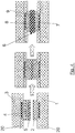
- Figure 1 shows an embodiment wherein a first substrate 1 is provided with a first micropattern 2, comprising a first high-melting metal A and a second substrate 3 is provided with a second micropattern 4, comprising a second high-melting metal C.
- a layer 5 of solder material B is applied, eg. a layer of Sn. The bonding will take place by bringing both substrates in contact and by applying a pressure and/or an increase in temperature, or by a reflow step, bonding takes place.
- a bonding structure 6 which comprises a first portion 7, in contact with the first substrate 1, said first portion corresponding to the first micropattern 2 and comprising the first high-melting metal A, a second portion 8, in contact with the second substrate 3, said second portion corresponding to the second micropattern 4 and comprising the second high-melting metal, and a middle portion 9, comprising solder material and/or one or more intermetallic compounds of the solder material and one or both of said high-melting metals.
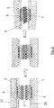
- a solder layer may be applied on one of the micropatterns (asymmetric embodiment, fig. 1 and 2 ), or on both of the micropatterns (symmetric embodiment, fig. 3 ).
- a thin layer of a metal D may be applied on the micropattern of the first substrate 1, i.e. on the micropattern 2 on which no solder layer is applied.
- Said metal layer D has the function of preventing oxidation of the underlying metal of the micropattern 2, and may also facilitate wetting by the solder layer 4.
- This material is preferably identical to the material B and will hereafter also be called 'solder' material.
- Layer D is preferably a thin layer that easily dissolves in the high-melting metal A and does not reduce the reaction between the metals B and C.
- Preferred material combinations are a thin Au layer (D) on a Cu pad (C) for Cu-Sn micropatterns or a thin Sn layer (D) on a Co pad (C) for Co-Sn micropatterns.
- a patterned layer or film 10 of a non-conductive adhesive material e.g. a uniform polymer layer is applied around (i.e. on both lateral sides of) at least one of the micropatterns which are to be joined.
- the adhesive layer extends on the whole surface of the substrate, outside of the micropatterns.
- the thickness of the adhesive layer(s) is such that during bonding, i.e. as the elements are brought closer together, the micropatterns make contact before the adhesive layer (s).
- the combined thickness of the glue layers 10 is slightly lower than the combined thickness (before bonding), of the micropatterns 2 and 4, and the two solder layers 5.
- the difference in thickness between the glue layer(s) and the combined micropattern/solder layer is preferably 1 to 5 micron.
- the distance between the glue layer ( fig. 3 ) or between the single glue layer and the opposite substrate is in the order of 1-5 micron. Only by approaching the elements further towards each other, the glue layer(s) make contact (see further).
- the adhesive layer is typically applied by spin-coating or spray-coating or lamination, but can be applied by other techniques known to a person of ordinary skill.
- the patterning of the uniform polymeric layer is preferably performed by photo patterning and wet development, but can be applied by other techniques known to a person of ordinary skill.
- the patterning step removes the polymer from the surface of the micro-patterns and leaves a small gap 11 between the micro-patterns and the remaining polymer layer.
- the width of the gap 11 is at least 1 micron and preferably not larger then 1/3 of the joined pattern height H, as shown in figure 3 . Larger gaps are not excluded but are expected to be less advantageous.
- a gap 12 is present between the joining structure 6 and the cured adhesive layer 13.
- the adhesive layer secures the elements together, and fulfills the same role as the known underfill material, applied after bonding according to prior art methods.
- the advantage of the present invention is that the adhesive layer is applied prior to bonding, so the problem of applying a standard capillary underfill after assembly in the narrow gap, is no longer relevant.
- the film 10 is then dried and the polymer in the film preferably remains in an incomplete curing-state to allow for reacting with the adhesive material of the other substrate (if such material is applied on both substrates) during the final curing applications.
- the glue material preferably doesn't produce any outgassing during the final curing step, as this may cause voiding and incomplete bonding.
- Typical materials that can be used for this application are photo-sensitive BCB (Cyclotene) from Dow Chemical and photo-sensitive silicones from Dow Corning, but other materials can be used which are known to a person of ordinary skill.
- the bonding is preferably performed in two steps.
- a first step the substrates are aligned with respect to each other and pre-bonded to each other.
- Pre-bonding can be performed at low temperature with lower forces.
- the temperature is preferably well below the curing temperature of the adhesive layer and well below the melting temperature of the solder material.
- the intention is that the solder material B of the top substrate 3 adheres sufficiently well to the solder metal B or to the non-oxidizing layer of the lower substrate 1, or to the micropattern 2 itself, if no solder nor a non-oxidizing layer is present. At this point, little interaction between the contacted metals occurs, but a weak bond is formed, sufficiently strong to maintain the alignment and contact between the two substrates during the subsequent handling. Also, no curing of the polymeric material takes place at this stage.
- the wafer formed by the pre-bonded substrates is preferably placed in a non-oxidizing ambient (for instance vacuum, nitrogen, forming-gas).
- a non-oxidizing ambient for instance vacuum, nitrogen, forming-gas.
- the wafer is pre-heated to a temperature below the melting point of the solder (metal B) and below the curing temperature of the polymer.
- the temperature is rapidly ramped up to a temperature whereby bonding occurs and if needed a uniform pressure is applied to the top substrate 3. This temperature is typically above the melting point of the solder, but can be performed below the melting point of the solder as well when an appropriate pressure is used.
- the solder metal B will interact with the corresponding solder metal B or cap metal D, or metal of the opposite micropattern.
- the liquid solder pattern will deform (collapse) as a result of the applied pressure at wafer level.
- the still un-cured polymer layer will make contact with the surface of the opposite substrate (a second polymer layer in the symmetric embodiments, the substrate passivation layer 20 in the asymmetric embodiments). Due to the high temperature, the polymer layer will deform and start curing. By further increasing the temperature, the curing reaction of the polymer may be accelerated to achieve a fully cured permanent adhesive layer that secures the bonding of the substrates after releasing the pressure between both substrates.
- the solder metals B form one common melt that interacts with both metals A and C.
- the solder metal B dissolves metal D and reacts with metal C.
- the different metals may dissolve and form alloys and/or generate intermetallic compounds.
- forces are used (from about 250 to about 400gf) for areas of a few square mm.
- the substrates After cooling down and removing the pressure, the substrates are permanently bonded.
- a solder layer or different alloys and intermetallic phases may be present in the intermetallic micro-pattern joints.
- a further annealing step may be used to fully transform the micropattern solder layers into a single intermetallic compound.
- the volume of solder metal B and D is of the same order or smaller than the metals A and C.
- the entire solder volume will be transformed into alloy or intermetallic compounds.
- the liquidus temperature of the melt will increase and a solidification of the melt may occur.
- the previous description is in fact a simplified illustration; it should be noted that the volume of solder material B and D will react with the metals A and C according to a certain ratio linked with the structure of the resulting intermetallic. For Co and thin Sn forming CoSn this ratio would be approximately 1:1. For Co and Sn forming CoSn2 this ratio would be 1:2, which means that twice as much solder will be consumed than metal when forming the intermetallic alloy.
- the micropatterns 2 and 4 are made of Co, and the solder is Sn.
- the specific combination of Co and Sn in the production and bonding of micropatterns as defined in the context of the present invention, is unknown in the art. Compared to other material combination (Cu and Sn for example), it has been found that the formation of the intermetallics during bonding takes place much faster when using Co and Sn, which provides a considerable advantage over the known combinations. For a similar amount of Sn and an equal reflow temperature of 250C, the full transition of Sn into Co-Sn intermetallic is more then 5 times faster compared to the transition into Cu - Sn intermetallics.
- a volume of Sn is applied such that the result is a bonding structure which comprises essentially only intermetallic compounds of Co and Sn, in particular CoSn or CoSn2, and no pure solder material.
- the thickness of the layers can be based on the following model and calculation:
- the intermetallic compounds of Co and Sn have other advantages over more traditional metal combinations, such as Cu/Sn:
- the Co/Sn may be used with and without the polymer adhesive layer 10. If no adhesive layer is used, a larger area of the die is preferably covered by micro-patterns to ensure mechanical stiffness.
- a micro-pattern solder ring on the perimeter of the device. This ring may be used to create a quasi-hermetically sealed cavity with micro-pattern connections. This technique is of particular interest for the bonding (capping) of MEMS devices.
- This micro-solder pattern can comprise and typically consists of two or more metal layers.
- the two top metal layers can consist of or comprise a high melting point metal A, such as Cu or and a low melting point metal B, such as Sn ('solder'). These metals should form intermetallic compounds or alloys when the temperature of the device approaches (solid state diffusion) or increases above the melting point (soldering) of the low melting temperature metal B.
- a preferred method for realizing the micro-patterns is semi-additive electroplating. Other methods known to a person of ordinary skill are also possible and include lift-off evaporation techniques.
- solder layers are prepared equally on both devices.
- the solder is applied only on the first device.
- solderable contact metallisations C are foreseen.
- This can preferably be the same material as the material A used as high melting point metal in the micro-pattern.
- This layer may be covered by a thin metal layer D that prevents oxidation of the bottom metal layer or improves the wetting of the low melting temperature metal B of the micro-pattern to the contact pad.
- This material is preferably identical to the material B or should be a thin layer that easily dissolves in the high temperature melting material A and does not reduce the reaction between the materials B and C.
- Preferred material combinations are a thin Au layer (D) on a Cu pad (C) for Cu-Sn micropatterns or a thin Sn layer (D) on a Co pad (C) for Co-Sn micropatterns.
- a uniform polymeric layer can be deposited on the device and patterned.
- this layer should have a thickness, slightly lower than the micro-solder pattern thickness, which is measured from the device substrate to the average top surface of the micro-patterns. This height thickness is typically 1-5 ⁇ m lower.
- this layer should have a thickness slightly lower than the combined thickness of the micro-pattern on the first device and contact pad metallisations on the second device. This layer is typically applied by spin-coating or spray-coating or lamination, but can be applied by other techniques known to a person of ordinary skill, some of which have been mentioned before.
- the patterning of the uniform polymeric layer is preferably performed by photo patterning and wet development, but can be applied by other techniques known to a person of ordinary skill.
- the patterning step removes the polymer from the surface of the micro-patterns and leaves a small gap between the micro-patterns and the remaining polymer layer.
- the film is dried and the polymer in the film preferably remains in an incomplete curing-state to allow for reacting with the material of the second device during the final curing applications.
- the material preferably doesn't produce any outgassing during the final curing step, as this may cause voiding and incomplete bonding.
- Typical materials that can be used for this application are photo-sensitive BCB (Cyclotene) from Dow Chemical and photo-sensitive silicones from Dow Corning, but other materials can be used which are known to a person of ordinary skill.
- the bonding is preferably performed in two steps.
- a first step the devices are aligned with respect to each other and pre-bonded to each other.
- Pre-bonding can be performed at low temperature with lower forces.
- the temperature is preferably well below the curing temperature of the polymeric adhesive layer and well below the melting temperature of the solder material.
- the intention is that the low melting point metal B of the top device adheres sufficiently well to the metal B or metal D of the lower device (method 1 or 2, respectively). At this point little interaction between the contacted metals occurs, but a weak bond is formed, sufficiently strong to maintain the alignment and contact between the two devices during the subsequent handling. Also, no curing of the polymeric material is preferred.
- This method allows for the placement of a large number of devices on a large base substrate (e.g. multi-die-to wafer bonding).
- the die-to-wafer process is a sequential process. Therefore, the time needed for the placement and pre-bonding should be minimized as much as possible. Therefore, the actual bonding is performed in a second, collective, processing step.
- the wafer is preferably placed in a non-oxidizing ambient (for instance vacuum, nitrogen, forming-gas).
- a non-oxidizing ambient for instance vacuum, nitrogen, forming-gas.
- the wafer is pre-heated to a temperature below the melting point of the solder (metal B) and below the curing temperature of the polymer.
- a Uniform pressure is applied over all die bonded to the base wafer and the temperature is rapidly ramped up to a temperature whereby bonding occurs. This is typically above the liquidus temperature of the solder, but can be performed below the melting point of the solder as well.
- the solder metal B will interact with the corresponding solder metal C (method 1) or cap metal D (method 2).
- the liquid micro-solder solder pattern will deform (collapse) as a result of the applied pressure at wafer level.
- the still un-cured polymer layer will make contact with the surface of the base substrate (a polymer layer in the symmetric embodiments, the substrate passivation layer in the asymmetric embodiments). Due to the high temperature, the polymer layer will deform and start curing. By further increasing the temperature, the curing reaction of the polymer may be accelerated to achieve a fully cured permanent glue layer that secures the die-wafer bonding after releasing the pressure between both wafers.
- the solder metals B and D form one common melt that interacts with both metals A and C.
- the solder metal B dissolves metal D and reacts with metal C.
- the different metals may dissolve and form alloys and/or generate intermetallic compounds.
- the volume of solder metal B and D is of the same order or smaller than the metals A and C.
- the volume of solder material B and D will react with the metals A and C according to a certain ratio linked with the structure of the resulting intermetallic. For Co and thin Sn forming CoSn this ratio would be approximately 1:1. For Co and Sn forming CoSn2 this ratio would be 1:2, which means that twice as much solder will be consumed than metal when forming the intermetallic alloy.
- the devices After cooling down and removing the pressure, the devices are permanently bonded.
- a solder layer or different alloys and intermetallic phases may be present in the intermetallic micro-pattern joints.
- a further annealing step may be used to fully transform the micropattern solder layers into a single intermetallic compound.
Landscapes
- Engineering & Computer Science (AREA)
- Microelectronics & Electronic Packaging (AREA)
- Computer Hardware Design (AREA)
- Power Engineering (AREA)
- Manufacturing & Machinery (AREA)
- Physics & Mathematics (AREA)
- Condensed Matter Physics & Semiconductors (AREA)
- General Physics & Mathematics (AREA)
- Ceramic Engineering (AREA)
- Wire Bonding (AREA)
- Electric Connection Of Electric Components To Printed Circuits (AREA)
Claims (5)
- Ein Verfahren zum Bonden zweier Elemente, umfassend:- Herstellen auf einem ersten Element (1) eines ersten Mikromusters (2), eine erste Metallschicht umfassend- Erzeugen auf einem zweiten Element (3) eines zweiten Mikromusters (4), eine zweite Metallschicht umfassend;- Aufbringen auf das erste Mikromuster und/oder auf das zweite Mikromuster einer Schicht (5) aus Lötmaterial;- Verbinden des ersten Mikromusters und des zweiten Mikromusters mittels eines Thermokompressions- oder Aufschmelzverfahrenswobei das erste und das zweite Mikromuster aus Cobalt (Co) hergestellt sind, und wobei die Lötmittelschicht eine Zinn (Sn)-Schicht ist,
dadurch gekennzeichnet, dass die Summe der Dicken der Cobalt-Mikromuster zumindest gleich einem Wert d ist, der bestimmt wird als:


- Das Verfahren nach Anspruch 1, wobei das Verfahren ferner den Schritt des Herstellens auf mindestens einem Element einer gemusterten nichtleitenden Klebeschicht (10) um das Mikromuster auf dem Element umfasst, wobei die Klebeschicht(en) vor dem Verbindungsschritt aufgebracht wird/werden, so dass nach dem Verbindungsschritt die Elemente durch die Klebeschicht(en) aneinander befestigt sind.
- Das Verfahren nach Anspruch 2, wobei die Klebeschicht so gemustert wird, das ein Spalt (11) zwischen der Klebeschicht und dem Mikromuster gelassen wird, um welche die Schicht aufgetragen wird.
- Das Verfahren nach Anspruch 3, wobei die Breite des Spalts (11) mindestens 1 µm beträgt, und nicht länger als 1/3 der Höhe (H) des verbundenen Musters ist.
- Das Verfahren nach einem der vorhergehenden Ansprüche, wobei die Klebeschicht (10) eine Polymerschicht, oder eine Schicht eines lichtempfindlichen BCBs (Benzocyclobutens) oder eines lichtempfindlichen Silikons ist.
Applications Claiming Priority (1)
| Application Number | Priority Date | Filing Date | Title |
|---|---|---|---|
| US68899405P | 2005-06-08 | 2005-06-08 |
Publications (3)
| Publication Number | Publication Date |
|---|---|
| EP1732116A2 EP1732116A2 (de) | 2006-12-13 |
| EP1732116A3 EP1732116A3 (de) | 2007-04-11 |
| EP1732116B1 true EP1732116B1 (de) | 2017-02-01 |
Family
ID=36676597
Family Applications (1)
| Application Number | Title | Priority Date | Filing Date |
|---|---|---|---|
| EP06114933.2A Active EP1732116B1 (de) | 2005-06-08 | 2006-06-02 | Methode zum Bonden mikroelektronischer Bauteile und damit hergestellte Vorrichtung |
Country Status (2)
| Country | Link |
|---|---|
| US (2) | US7547625B2 (de) |
| EP (1) | EP1732116B1 (de) |
Families Citing this family (68)
| Publication number | Priority date | Publication date | Assignee | Title |
|---|---|---|---|---|
| US7851348B2 (en) | 2005-06-14 | 2010-12-14 | Abhay Misra | Routingless chip architecture |
| US7786592B2 (en) | 2005-06-14 | 2010-08-31 | John Trezza | Chip capacitive coupling |
| US7687400B2 (en) | 2005-06-14 | 2010-03-30 | John Trezza | Side stacking apparatus and method |
| US7767493B2 (en) | 2005-06-14 | 2010-08-03 | John Trezza | Post & penetration interconnection |
| US7946331B2 (en) | 2005-06-14 | 2011-05-24 | Cufer Asset Ltd. L.L.C. | Pin-type chip tooling |
| US7781886B2 (en) | 2005-06-14 | 2010-08-24 | John Trezza | Electronic chip contact structure |
| US8456015B2 (en) | 2005-06-14 | 2013-06-04 | Cufer Asset Ltd. L.L.C. | Triaxial through-chip connection |
| US7838997B2 (en) | 2005-06-14 | 2010-11-23 | John Trezza | Remote chip attachment |
| US7560813B2 (en) | 2005-06-14 | 2009-07-14 | John Trezza | Chip-based thermo-stack |
| US20070099410A1 (en) * | 2005-10-31 | 2007-05-03 | Sawyer William D | Hard intermetallic bonding of wafers for MEMS applications |
| US7579258B2 (en) * | 2006-01-25 | 2009-08-25 | Freescale Semiconductor, Inc. | Semiconductor interconnect having adjacent reservoir for bonding and method for formation |
| TWI295840B (en) * | 2006-04-07 | 2008-04-11 | Advanced Semiconductor Eng | Mounting method of passive component |
| US7476570B2 (en) * | 2006-05-02 | 2009-01-13 | Honeywell International Inc. | System and method of attaching an integrated circuit assembly to a printed wiring board |
| US7687397B2 (en) | 2006-06-06 | 2010-03-30 | John Trezza | Front-end processed wafer having through-chip connections |
| US20080164606A1 (en) * | 2007-01-08 | 2008-07-10 | Christoffer Graae Greisen | Spacers for wafer bonding |
| US7670874B2 (en) | 2007-02-16 | 2010-03-02 | John Trezza | Plated pillar package formation |
| JP5159273B2 (ja) | 2007-11-28 | 2013-03-06 | ルネサスエレクトロニクス株式会社 | 電子装置の製造方法 |
| JP5277068B2 (ja) * | 2008-07-14 | 2013-08-28 | パナソニック株式会社 | 基板間の接続方法、フリップチップ実装体及び基板間接続構造 |
| EP2340554B1 (de) * | 2008-09-18 | 2017-05-10 | Imec | Verfahren und systeme zum bonden von materialien |
| DE102009009828A1 (de) | 2009-02-19 | 2010-09-02 | Fraunhofer-Gesellschaft zur Förderung der angewandten Forschung e.V. | Bauteilanordnung und Verfahren zu dessen Herstellung |
| US7939369B2 (en) | 2009-05-14 | 2011-05-10 | International Business Machines Corporation | 3D integration structure and method using bonded metal planes |
| KR101234597B1 (ko) * | 2009-10-15 | 2013-02-22 | 한국전자통신연구원 | 플립 칩 본딩 방법 및 그의 구조 |
| US8138019B2 (en) * | 2009-11-03 | 2012-03-20 | Toyota Motor Engineering & Manufactruing North America, Inc. | Integrated (multilayer) circuits and process of producing the same |
| EP2363373A1 (de) | 2010-03-02 | 2011-09-07 | SensoNor Technologies AS | Procédé de collage pour systèmes micro et nano sensibles |
| EP2654075B1 (de) * | 2010-03-31 | 2016-09-28 | EV Group E. Thallner GmbH | Verfahren zum permanenten Verbinden zweier Metalloberflächen |
| US9142533B2 (en) | 2010-05-20 | 2015-09-22 | Taiwan Semiconductor Manufacturing Company, Ltd. | Substrate interconnections having different sizes |
| US8268716B2 (en) * | 2010-09-30 | 2012-09-18 | International Business Machines Corporation | Creation of lead-free solder joint with intermetallics |
| US8802553B2 (en) | 2011-02-10 | 2014-08-12 | Infineon Technologies Ag | Method for mounting a semiconductor chip on a carrier |
| CN102244022A (zh) * | 2011-04-26 | 2011-11-16 | 哈尔滨工业大学 | 倒装芯片单金属间化合物微互连结构制备方法 |
| CN102820268B (zh) * | 2011-06-10 | 2016-01-20 | 华进半导体封装先导技术研发中心有限公司 | 键合结构及其制备方法 |
| CN102999382A (zh) * | 2011-09-09 | 2013-03-27 | 鸿富锦精密工业(深圳)有限公司 | 电子设备及其切换方法 |
| US8349116B1 (en) | 2011-11-18 | 2013-01-08 | LuxVue Technology Corporation | Micro device transfer head heater assembly and method of transferring a micro device |
| US8426227B1 (en) | 2011-11-18 | 2013-04-23 | LuxVue Technology Corporation | Method of forming a micro light emitting diode array |
| US8575748B1 (en) | 2011-12-13 | 2013-11-05 | Sandia Corporation | Wafer-level packaging with compression-controlled seal ring bonding |
| US9773750B2 (en) | 2012-02-09 | 2017-09-26 | Apple Inc. | Method of transferring and bonding an array of micro devices |
| US8697542B2 (en) | 2012-04-12 | 2014-04-15 | The Research Foundation Of State University Of New York | Method for thin die-to-wafer bonding |
| US9425136B2 (en) | 2012-04-17 | 2016-08-23 | Taiwan Semiconductor Manufacturing Company, Ltd. | Conical-shaped or tier-shaped pillar connections |
| US9646923B2 (en) | 2012-04-17 | 2017-05-09 | Taiwan Semiconductor Manufacturing Company, Ltd. | Semiconductor devices, methods of manufacture thereof, and packaged semiconductor devices |
| US9299674B2 (en) | 2012-04-18 | 2016-03-29 | Taiwan Semiconductor Manufacturing Company, Ltd. | Bump-on-trace interconnect |
| US8994190B2 (en) * | 2012-05-22 | 2015-03-31 | Freescale Semiconductor, Inc. | Low-temperature flip chip die attach |
| JP6044885B2 (ja) * | 2012-08-08 | 2016-12-14 | パナソニックIpマネジメント株式会社 | 実装方法 |
| US9111817B2 (en) | 2012-09-18 | 2015-08-18 | Taiwan Semiconductor Manufacturing Company, Ltd. | Bump structure and method of forming same |
| CN103043605B (zh) * | 2012-12-07 | 2015-11-18 | 中国电子科技集团公司第五十五研究所 | 微型电镀立体结构提高圆片级金属键合强度的工艺方法 |
| US9082681B2 (en) * | 2013-03-29 | 2015-07-14 | Stmicroelectronics Pte Ltd. | Adhesive bonding technique for use with capacitive micro-sensors |
| US9618653B2 (en) | 2013-03-29 | 2017-04-11 | Stmicroelectronics Pte Ltd. | Microelectronic environmental sensing module |
| US9176089B2 (en) | 2013-03-29 | 2015-11-03 | Stmicroelectronics Pte Ltd. | Integrated multi-sensor module |
| US9000542B2 (en) | 2013-05-31 | 2015-04-07 | Stmicroelectronics Pte Ltd. | Suspended membrane device |
| US9355980B2 (en) | 2013-09-03 | 2016-05-31 | Taiwan Semiconductor Manufacturing Company, Ltd. | Three-dimensional chip stack and method of forming the same |
| JP6424610B2 (ja) * | 2014-04-23 | 2018-11-21 | ソニー株式会社 | 半導体装置、および製造方法 |
| WO2016007092A1 (en) * | 2014-07-09 | 2016-01-14 | Agency For Science, Technology And Research | A method for low temperature bonding of wafers |
| SG10201903641TA (en) * | 2014-10-23 | 2019-05-30 | Agency Science Tech & Res | Method of bonding a first substrate and a second substrate |
| US9935072B2 (en) | 2015-11-04 | 2018-04-03 | Sfa Semicon Co., Ltd. | Semiconductor package and method for manufacturing the same |
| KR101806141B1 (ko) * | 2015-11-04 | 2017-12-07 | 주식회사 에스에프에이반도체 | 적층형 반도체 패키지 및 그 제조 방법 |
| JP6534948B2 (ja) * | 2016-02-26 | 2019-06-26 | 信越化学工業株式会社 | 半導体装置の製造方法、フリップチップ型半導体装置の製造方法、半導体装置及びフリップチップ型半導体装置 |
| US10254261B2 (en) | 2016-07-18 | 2019-04-09 | Stmicroelectronics Pte Ltd | Integrated air quality sensor that detects multiple gas species |
| US10429330B2 (en) | 2016-07-18 | 2019-10-01 | Stmicroelectronics Pte Ltd | Gas analyzer that detects gases, humidity, and temperature |
| US9761542B1 (en) * | 2016-09-07 | 2017-09-12 | International Business Machines Corporation | Liquid metal flip chip devices |
| US10557812B2 (en) | 2016-12-01 | 2020-02-11 | Stmicroelectronics Pte Ltd | Gas sensors |
| US10290611B2 (en) * | 2017-07-27 | 2019-05-14 | Taiwan Semiconductor Manufacturing Company, Ltd. | Semiconductor packages and methods of forming same |
| US10340249B1 (en) * | 2018-06-25 | 2019-07-02 | Taiwan Semiconductor Manufacturing Company, Ltd. | Semiconductor device and method |
| TWI697078B (zh) * | 2018-08-03 | 2020-06-21 | 欣興電子股份有限公司 | 封裝基板結構與其接合方法 |
| CN113439332A (zh) * | 2019-02-21 | 2021-09-24 | 维耶尔公司 | 光电固态阵列 |
| EP3754706A1 (de) | 2019-06-20 | 2020-12-23 | IMEC vzw | Verfahren zur elektrischen verbindung von halbleiterkomponenten |
| DE102020202613A1 (de) | 2020-03-02 | 2021-09-02 | OSRAM Opto Semiconductors Gesellschaft mit beschränkter Haftung | Verfahren zur herstellung eines halbleiterbauelements, halbleiterbauelement und optoelektronische vorrichtung |
| US11329023B2 (en) * | 2020-04-10 | 2022-05-10 | Schlumberger Technology Corporation | Interconnection of copper surfaces using copper sintering material |
| DE102020206763A1 (de) | 2020-05-29 | 2021-12-02 | Siemens Aktiengesellschaft | Fügen und Isolieren von leistungselektronischen Halbleiterbauteilen |
| CN113130336A (zh) * | 2021-04-16 | 2021-07-16 | 中国电子科技集团公司第二十四研究所 | 一种基板预植Au凸点的倒装焊工艺方法 |
| CN116762167A (zh) * | 2021-05-10 | 2023-09-15 | 华为技术有限公司 | 集成电路堆叠结构及其制作方法、电子设备 |
Family Cites Families (21)
| Publication number | Priority date | Publication date | Assignee | Title |
|---|---|---|---|---|
| JPH07112041B2 (ja) * | 1986-12-03 | 1995-11-29 | シャープ株式会社 | 半導体装置の製造方法 |
| JPH0732158B2 (ja) * | 1988-04-08 | 1995-04-10 | インターナシヨナル・ビジネス・マシーンズ・コーポレーシヨン | 電子部品のための多層金属構造 |
| US5074947A (en) * | 1989-12-18 | 1991-12-24 | Epoxy Technology, Inc. | Flip chip technology using electrically conductive polymers and dielectrics |
| US5503286A (en) * | 1994-06-28 | 1996-04-02 | International Business Machines Corporation | Electroplated solder terminal |
| US5844315A (en) | 1996-03-26 | 1998-12-01 | Motorola Corporation | Low-profile microelectronic package |
| US6121689A (en) | 1997-07-21 | 2000-09-19 | Miguel Albert Capote | Semiconductor flip-chip package and method for the fabrication thereof |
| US6002172A (en) * | 1997-03-12 | 1999-12-14 | International Business Machines Corporation | Substrate structure and method for improving attachment reliability of semiconductor chips and modules |
| EP1010781A4 (de) * | 1997-04-17 | 2007-04-25 | Sekisui Chemical Co Ltd | Leitende teilchen und verfahren und vorrichtung zur herstellung derselben, anisotropes leitendes adhesiv und leitende verbindungsstruktur und elektrische schaltkomponenten und verfahren zu deren herstellung |
| JP3070514B2 (ja) | 1997-04-28 | 2000-07-31 | 日本電気株式会社 | 突起電極を有する半導体装置、半導体装置の実装方法およびその実装構造 |
| JP3451987B2 (ja) * | 1998-07-01 | 2003-09-29 | 日本電気株式会社 | 機能素子及び機能素子搭載用基板並びにそれらの接続方法 |
| US6168972B1 (en) | 1998-12-22 | 2001-01-02 | Fujitsu Limited | Flip chip pre-assembly underfill process |
| TW460927B (en) * | 1999-01-18 | 2001-10-21 | Toshiba Corp | Semiconductor device, mounting method for semiconductor device and manufacturing method for semiconductor device |
| US6190940B1 (en) * | 1999-01-21 | 2001-02-20 | Lucent Technologies Inc. | Flip chip assembly of semiconductor IC chips |
| SG106054A1 (en) | 2001-04-17 | 2004-09-30 | Micron Technology Inc | Method and apparatus for package reduction in stacked chip and board assemblies |
| JP3866591B2 (ja) * | 2001-10-29 | 2007-01-10 | 富士通株式会社 | 電極間接続構造体の形成方法および電極間接続構造体 |
| US6908784B1 (en) | 2002-03-06 | 2005-06-21 | Micron Technology, Inc. | Method for fabricating encapsulated semiconductor components |
| US20040096592A1 (en) * | 2002-11-19 | 2004-05-20 | Chebiam Ramanan V. | Electroless cobalt plating solution and plating techniques |
| US6720246B1 (en) * | 2003-01-23 | 2004-04-13 | Silicon Integrated Systems Corp. | Flip chip assembly process for forming an underfill encapsulant |
| US6821878B2 (en) * | 2003-02-27 | 2004-11-23 | Freescale Semiconductor, Inc. | Area-array device assembly with pre-applied underfill layers on printed wiring board |
| US7242097B2 (en) * | 2003-06-30 | 2007-07-10 | Intel Corporation | Electromigration barrier layers for solder joints |
| TWI230989B (en) * | 2004-05-05 | 2005-04-11 | Megic Corp | Chip bonding method |
-
2006
- 2006-06-02 EP EP06114933.2A patent/EP1732116B1/de active Active
- 2006-06-07 US US11/448,598 patent/US7547625B2/en active Active
-
2009
- 2009-05-11 US US12/463,960 patent/US7880315B2/en active Active
Non-Patent Citations (1)
| Title |
|---|
| None * |
Also Published As
| Publication number | Publication date |
|---|---|
| US20090218702A1 (en) | 2009-09-03 |
| EP1732116A3 (de) | 2007-04-11 |
| US20060292824A1 (en) | 2006-12-28 |
| US7547625B2 (en) | 2009-06-16 |
| US7880315B2 (en) | 2011-02-01 |
| EP1732116A2 (de) | 2006-12-13 |
Similar Documents
| Publication | Publication Date | Title |
|---|---|---|
| EP1732116B1 (de) | Methode zum Bonden mikroelektronischer Bauteile und damit hergestellte Vorrichtung | |
| US7713782B2 (en) | Fusible I/O interconnection systems and methods for flip-chip packaging involving substrate-mounted stud-bumps | |
| US6740960B1 (en) | Semiconductor package including flex circuit, interconnects and dense array external contacts | |
| US6097087A (en) | Semiconductor package including flex circuit, interconnects and dense array external contacts | |
| US5937320A (en) | Barrier layers for electroplated SnPb eutectic solder joints | |
| US20110177686A1 (en) | Stable Gold Bump Solder Connections | |
| US20040087057A1 (en) | Method for fabricating a flip chip package with pillar bump and no flow underfill | |
| EP2340554B1 (de) | Verfahren und systeme zum bonden von materialien | |
| US8119450B2 (en) | Interconnecting a chip and a substrate by bonding pure metal bumps and pure metal spots | |
| US7993971B2 (en) | Forming a 3-D semiconductor die structure with an intermetallic formation | |
| Tu et al. | Electronic packaging science and technology | |
| JP6593119B2 (ja) | 電極構造、接合方法及び半導体装置 | |
| US8735277B2 (en) | Methods for producing an ultrathin semiconductor circuit | |
| Jung et al. | Reliability investigations of different bumping processes for flip chip and TAB applications | |
| Kallmayer et al. | Reliability investigations of flip-chip solder bumps on palladium | |
| Ong et al. | Thin die stacking by low temperature in/Au IMC based bonding method |
Legal Events
| Date | Code | Title | Description |
|---|---|---|---|
| PUAI | Public reference made under article 153(3) epc to a published international application that has entered the european phase |
Free format text: ORIGINAL CODE: 0009012 |
|
| AK | Designated contracting states |
Kind code of ref document: A2 Designated state(s): AT BE BG CH CY CZ DE DK EE ES FI FR GB GR HU IE IS IT LI LT LU LV MC NL PL PT RO SE SI SK TR |
|
| AX | Request for extension of the european patent |
Extension state: AL BA HR MK YU |
|
| PUAL | Search report despatched |
Free format text: ORIGINAL CODE: 0009013 |
|
| AK | Designated contracting states |
Kind code of ref document: A3 Designated state(s): AT BE BG CH CY CZ DE DK EE ES FI FR GB GR HU IE IS IT LI LT LU LV MC NL PL PT RO SE SI SK TR |
|
| AX | Request for extension of the european patent |
Extension state: AL BA HR MK YU |
|
| 17P | Request for examination filed |
Effective date: 20070629 |
|
| 17Q | First examination report despatched |
Effective date: 20070829 |
|
| AKX | Designation fees paid |
Designated state(s): AT BE BG CH CY CZ DE DK EE ES FI FR GB GR HU IE IS IT LI LT LU LV MC NL PL PT RO SE SI SK TR |
|
| RAP1 | Party data changed (applicant data changed or rights of an application transferred) |
Owner name: IMEC |
|
| GRAP | Despatch of communication of intention to grant a patent |
Free format text: ORIGINAL CODE: EPIDOSNIGR1 |
|
| INTG | Intention to grant announced |
Effective date: 20160826 |
|
| GRAS | Grant fee paid |
Free format text: ORIGINAL CODE: EPIDOSNIGR3 |
|
| GRAA | (expected) grant |
Free format text: ORIGINAL CODE: 0009210 |
|
| AK | Designated contracting states |
Kind code of ref document: B1 Designated state(s): AT BE BG CH CY CZ DE DK EE ES FI FR GB GR HU IE IS IT LI LT LU LV MC NL PL PT RO SE SI SK TR |
|
| REG | Reference to a national code |
Ref country code: GB Ref legal event code: FG4D |
|
| REG | Reference to a national code |
Ref country code: CH Ref legal event code: EP Ref country code: AT Ref legal event code: REF Ref document number: 866197 Country of ref document: AT Kind code of ref document: T Effective date: 20170215 |
|
| REG | Reference to a national code |
Ref country code: IE Ref legal event code: FG4D |
|
| REG | Reference to a national code |
Ref country code: DE Ref legal event code: R096 Ref document number: 602006051673 Country of ref document: DE |
|
| REG | Reference to a national code |
Ref country code: FR Ref legal event code: PLFP Year of fee payment: 12 |
|
| REG | Reference to a national code |
Ref country code: NL Ref legal event code: MP Effective date: 20170201 |
|
| REG | Reference to a national code |
Ref country code: LT Ref legal event code: MG4D |
|
| REG | Reference to a national code |
Ref country code: AT Ref legal event code: MK05 Ref document number: 866197 Country of ref document: AT Kind code of ref document: T Effective date: 20170201 |
|
| PG25 | Lapsed in a contracting state [announced via postgrant information from national office to epo] |
Ref country code: LT Free format text: LAPSE BECAUSE OF FAILURE TO SUBMIT A TRANSLATION OF THE DESCRIPTION OR TO PAY THE FEE WITHIN THE PRESCRIBED TIME-LIMIT Effective date: 20170201 Ref country code: IS Free format text: LAPSE BECAUSE OF FAILURE TO SUBMIT A TRANSLATION OF THE DESCRIPTION OR TO PAY THE FEE WITHIN THE PRESCRIBED TIME-LIMIT Effective date: 20170601 Ref country code: FI Free format text: LAPSE BECAUSE OF FAILURE TO SUBMIT A TRANSLATION OF THE DESCRIPTION OR TO PAY THE FEE WITHIN THE PRESCRIBED TIME-LIMIT Effective date: 20170201 Ref country code: GR Free format text: LAPSE BECAUSE OF FAILURE TO SUBMIT A TRANSLATION OF THE DESCRIPTION OR TO PAY THE FEE WITHIN THE PRESCRIBED TIME-LIMIT Effective date: 20170502 |
|
| PG25 | Lapsed in a contracting state [announced via postgrant information from national office to epo] |
Ref country code: LV Free format text: LAPSE BECAUSE OF FAILURE TO SUBMIT A TRANSLATION OF THE DESCRIPTION OR TO PAY THE FEE WITHIN THE PRESCRIBED TIME-LIMIT Effective date: 20170201 Ref country code: NL Free format text: LAPSE BECAUSE OF FAILURE TO SUBMIT A TRANSLATION OF THE DESCRIPTION OR TO PAY THE FEE WITHIN THE PRESCRIBED TIME-LIMIT Effective date: 20170201 Ref country code: PT Free format text: LAPSE BECAUSE OF FAILURE TO SUBMIT A TRANSLATION OF THE DESCRIPTION OR TO PAY THE FEE WITHIN THE PRESCRIBED TIME-LIMIT Effective date: 20170601 Ref country code: ES Free format text: LAPSE BECAUSE OF FAILURE TO SUBMIT A TRANSLATION OF THE DESCRIPTION OR TO PAY THE FEE WITHIN THE PRESCRIBED TIME-LIMIT Effective date: 20170201 Ref country code: BG Free format text: LAPSE BECAUSE OF FAILURE TO SUBMIT A TRANSLATION OF THE DESCRIPTION OR TO PAY THE FEE WITHIN THE PRESCRIBED TIME-LIMIT Effective date: 20170501 Ref country code: AT Free format text: LAPSE BECAUSE OF FAILURE TO SUBMIT A TRANSLATION OF THE DESCRIPTION OR TO PAY THE FEE WITHIN THE PRESCRIBED TIME-LIMIT Effective date: 20170201 Ref country code: SE Free format text: LAPSE BECAUSE OF FAILURE TO SUBMIT A TRANSLATION OF THE DESCRIPTION OR TO PAY THE FEE WITHIN THE PRESCRIBED TIME-LIMIT Effective date: 20170201 Ref country code: PL Free format text: LAPSE BECAUSE OF FAILURE TO SUBMIT A TRANSLATION OF THE DESCRIPTION OR TO PAY THE FEE WITHIN THE PRESCRIBED TIME-LIMIT Effective date: 20170201 |
|
| PG25 | Lapsed in a contracting state [announced via postgrant information from national office to epo] |
Ref country code: EE Free format text: LAPSE BECAUSE OF FAILURE TO SUBMIT A TRANSLATION OF THE DESCRIPTION OR TO PAY THE FEE WITHIN THE PRESCRIBED TIME-LIMIT Effective date: 20170201 Ref country code: CZ Free format text: LAPSE BECAUSE OF FAILURE TO SUBMIT A TRANSLATION OF THE DESCRIPTION OR TO PAY THE FEE WITHIN THE PRESCRIBED TIME-LIMIT Effective date: 20170201 Ref country code: IT Free format text: LAPSE BECAUSE OF FAILURE TO SUBMIT A TRANSLATION OF THE DESCRIPTION OR TO PAY THE FEE WITHIN THE PRESCRIBED TIME-LIMIT Effective date: 20170201 Ref country code: SK Free format text: LAPSE BECAUSE OF FAILURE TO SUBMIT A TRANSLATION OF THE DESCRIPTION OR TO PAY THE FEE WITHIN THE PRESCRIBED TIME-LIMIT Effective date: 20170201 Ref country code: RO Free format text: LAPSE BECAUSE OF FAILURE TO SUBMIT A TRANSLATION OF THE DESCRIPTION OR TO PAY THE FEE WITHIN THE PRESCRIBED TIME-LIMIT Effective date: 20170201 |
|
| REG | Reference to a national code |
Ref country code: DE Ref legal event code: R097 Ref document number: 602006051673 Country of ref document: DE |
|
| PG25 | Lapsed in a contracting state [announced via postgrant information from national office to epo] |
Ref country code: DK Free format text: LAPSE BECAUSE OF FAILURE TO SUBMIT A TRANSLATION OF THE DESCRIPTION OR TO PAY THE FEE WITHIN THE PRESCRIBED TIME-LIMIT Effective date: 20170201 |
|
| PLBE | No opposition filed within time limit |
Free format text: ORIGINAL CODE: 0009261 |
|
| STAA | Information on the status of an ep patent application or granted ep patent |
Free format text: STATUS: NO OPPOSITION FILED WITHIN TIME LIMIT |
|
| RAP2 | Party data changed (patent owner data changed or rights of a patent transferred) |
Owner name: IMEC VZW |
|
| 26N | No opposition filed |
Effective date: 20171103 |
|
| PG25 | Lapsed in a contracting state [announced via postgrant information from national office to epo] |
Ref country code: MC Free format text: LAPSE BECAUSE OF FAILURE TO SUBMIT A TRANSLATION OF THE DESCRIPTION OR TO PAY THE FEE WITHIN THE PRESCRIBED TIME-LIMIT Effective date: 20170201 |
|
| REG | Reference to a national code |
Ref country code: CH Ref legal event code: PL |
|
| GBPC | Gb: european patent ceased through non-payment of renewal fee |
Effective date: 20170602 |
|
| PG25 | Lapsed in a contracting state [announced via postgrant information from national office to epo] |
Ref country code: SI Free format text: LAPSE BECAUSE OF FAILURE TO SUBMIT A TRANSLATION OF THE DESCRIPTION OR TO PAY THE FEE WITHIN THE PRESCRIBED TIME-LIMIT Effective date: 20170201 |
|
| REG | Reference to a national code |
Ref country code: IE Ref legal event code: MM4A |
|
| PG25 | Lapsed in a contracting state [announced via postgrant information from national office to epo] |
Ref country code: LI Free format text: LAPSE BECAUSE OF NON-PAYMENT OF DUE FEES Effective date: 20170630 Ref country code: CH Free format text: LAPSE BECAUSE OF NON-PAYMENT OF DUE FEES Effective date: 20170630 Ref country code: IE Free format text: LAPSE BECAUSE OF NON-PAYMENT OF DUE FEES Effective date: 20170602 Ref country code: GB Free format text: LAPSE BECAUSE OF NON-PAYMENT OF DUE FEES Effective date: 20170602 Ref country code: LU Free format text: LAPSE BECAUSE OF NON-PAYMENT OF DUE FEES Effective date: 20170602 |
|
| REG | Reference to a national code |
Ref country code: FR Ref legal event code: PLFP Year of fee payment: 13 |
|
| REG | Reference to a national code |
Ref country code: BE Ref legal event code: MM Effective date: 20170630 |
|
| PG25 | Lapsed in a contracting state [announced via postgrant information from national office to epo] |
Ref country code: BE Free format text: LAPSE BECAUSE OF NON-PAYMENT OF DUE FEES Effective date: 20170630 |
|
| PG25 | Lapsed in a contracting state [announced via postgrant information from national office to epo] |
Ref country code: HU Free format text: LAPSE BECAUSE OF FAILURE TO SUBMIT A TRANSLATION OF THE DESCRIPTION OR TO PAY THE FEE WITHIN THE PRESCRIBED TIME-LIMIT; INVALID AB INITIO Effective date: 20060602 |
|
| PG25 | Lapsed in a contracting state [announced via postgrant information from national office to epo] |
Ref country code: CY Free format text: LAPSE BECAUSE OF NON-PAYMENT OF DUE FEES Effective date: 20170201 |
|
| PG25 | Lapsed in a contracting state [announced via postgrant information from national office to epo] |
Ref country code: TR Free format text: LAPSE BECAUSE OF FAILURE TO SUBMIT A TRANSLATION OF THE DESCRIPTION OR TO PAY THE FEE WITHIN THE PRESCRIBED TIME-LIMIT Effective date: 20170201 |
|
| P01 | Opt-out of the competence of the unified patent court (upc) registered |
Effective date: 20230513 |
|
| PGFP | Annual fee paid to national office [announced via postgrant information from national office to epo] |
Ref country code: FR Payment date: 20230523 Year of fee payment: 18 Ref country code: DE Payment date: 20230523 Year of fee payment: 18 |