EP1728067B1 - Colorimetric sensor - Google Patents
Colorimetric sensor Download PDFInfo
- Publication number
- EP1728067B1 EP1728067B1 EP05779476A EP05779476A EP1728067B1 EP 1728067 B1 EP1728067 B1 EP 1728067B1 EP 05779476 A EP05779476 A EP 05779476A EP 05779476 A EP05779476 A EP 05779476A EP 1728067 B1 EP1728067 B1 EP 1728067B1
- Authority
- EP
- European Patent Office
- Prior art keywords
- layer
- semi
- reflective layer
- reflective
- sensor
- Prior art date
- Legal status (The legal status is an assumption and is not a legal conclusion. Google has not performed a legal analysis and makes no representation as to the accuracy of the status listed.)
- Expired - Lifetime
Links
- 238000001514 detection method Methods 0.000 claims abstract description 181
- 238000000034 method Methods 0.000 claims abstract description 40
- 239000010410 layer Substances 0.000 claims description 457
- 239000012491 analyte Substances 0.000 claims description 80
- 239000000463 material Substances 0.000 claims description 43
- 230000008859 change Effects 0.000 claims description 33
- 229920000642 polymer Polymers 0.000 claims description 33
- 230000003287 optical effect Effects 0.000 claims description 21
- 239000002356 single layer Substances 0.000 claims description 10
- 230000035699 permeability Effects 0.000 claims description 8
- 238000012544 monitoring process Methods 0.000 claims description 6
- 230000000873 masking effect Effects 0.000 claims description 5
- 239000012466 permeate Substances 0.000 claims description 5
- 239000010408 film Substances 0.000 description 101
- -1 poly(dimethylsiloxane) Polymers 0.000 description 49
- NIXOWILDQLNWCW-UHFFFAOYSA-M Acrylate Chemical compound [O-]C(=O)C=C NIXOWILDQLNWCW-UHFFFAOYSA-M 0.000 description 34
- 239000000178 monomer Substances 0.000 description 29
- YXFVVABEGXRONW-UHFFFAOYSA-N Toluene Chemical compound CC1=CC=CC=C1 YXFVVABEGXRONW-UHFFFAOYSA-N 0.000 description 27
- 239000000203 mixture Substances 0.000 description 23
- CSCPPACGZOOCGX-UHFFFAOYSA-N Acetone Chemical compound CC(C)=O CSCPPACGZOOCGX-UHFFFAOYSA-N 0.000 description 20
- 239000011651 chromium Substances 0.000 description 20
- 239000000758 substrate Substances 0.000 description 20
- 239000011148 porous material Substances 0.000 description 19
- WEVYAHXRMPXWCK-UHFFFAOYSA-N Acetonitrile Chemical compound CC#N WEVYAHXRMPXWCK-UHFFFAOYSA-N 0.000 description 15
- YMWUJEATGCHHMB-UHFFFAOYSA-N Dichloromethane Chemical compound ClCCl YMWUJEATGCHHMB-UHFFFAOYSA-N 0.000 description 14
- LFQSCWFLJHTTHZ-UHFFFAOYSA-N Ethanol Chemical compound CCO LFQSCWFLJHTTHZ-UHFFFAOYSA-N 0.000 description 14
- 239000000126 substance Substances 0.000 description 14
- XLYOFNOQVPJJNP-UHFFFAOYSA-N water Chemical compound O XLYOFNOQVPJJNP-UHFFFAOYSA-N 0.000 description 14
- 230000004044 response Effects 0.000 description 13
- 229910010272 inorganic material Inorganic materials 0.000 description 12
- 239000011147 inorganic material Substances 0.000 description 12
- 239000007788 liquid Substances 0.000 description 12
- 229910052751 metal Inorganic materials 0.000 description 12
- 239000002184 metal Substances 0.000 description 12
- 238000003491 array Methods 0.000 description 11
- 229910052782 aluminium Inorganic materials 0.000 description 10
- XAGFODPZIPBFFR-UHFFFAOYSA-N aluminium Chemical compound [Al] XAGFODPZIPBFFR-UHFFFAOYSA-N 0.000 description 10
- 239000002904 solvent Substances 0.000 description 10
- ZWEHNKRNPOVVGH-UHFFFAOYSA-N 2-Butanone Chemical compound CCC(C)=O ZWEHNKRNPOVVGH-UHFFFAOYSA-N 0.000 description 9
- 238000000151 deposition Methods 0.000 description 9
- WYURNTSHIVDZCO-UHFFFAOYSA-N Tetrahydrofuran Chemical compound C1CCOC1 WYURNTSHIVDZCO-UHFFFAOYSA-N 0.000 description 8
- 229920000728 polyester Polymers 0.000 description 8
- HEDRZPFGACZZDS-UHFFFAOYSA-N Chloroform Chemical compound ClC(Cl)Cl HEDRZPFGACZZDS-UHFFFAOYSA-N 0.000 description 7
- 239000007789 gas Substances 0.000 description 7
- 239000013316 polymer of intrinsic microporosity Substances 0.000 description 7
- 230000008569 process Effects 0.000 description 7
- LYCAIKOWRPUZTN-UHFFFAOYSA-N Ethylene glycol Chemical compound OCCO LYCAIKOWRPUZTN-UHFFFAOYSA-N 0.000 description 6
- 230000008021 deposition Effects 0.000 description 6
- 238000004528 spin coating Methods 0.000 description 6
- CURLTUGMZLYLDI-UHFFFAOYSA-N Carbon dioxide Chemical compound O=C=O CURLTUGMZLYLDI-UHFFFAOYSA-N 0.000 description 5
- VYZAMTAEIAYCRO-UHFFFAOYSA-N Chromium Chemical compound [Cr] VYZAMTAEIAYCRO-UHFFFAOYSA-N 0.000 description 5
- 150000001252 acrylic acid derivatives Chemical class 0.000 description 5
- 229910052804 chromium Inorganic materials 0.000 description 5
- 239000011248 coating agent Substances 0.000 description 5
- 238000000576 coating method Methods 0.000 description 5
- 238000010276 construction Methods 0.000 description 5
- 238000005530 etching Methods 0.000 description 5
- 239000011521 glass Substances 0.000 description 5
- 230000002441 reversible effect Effects 0.000 description 5
- 230000035945 sensitivity Effects 0.000 description 5
- HRPVXLWXLXDGHG-UHFFFAOYSA-N Acrylamide Chemical compound NC(=O)C=C HRPVXLWXLXDGHG-UHFFFAOYSA-N 0.000 description 4
- PXHVJJICTQNCMI-UHFFFAOYSA-N Nickel Chemical compound [Ni] PXHVJJICTQNCMI-UHFFFAOYSA-N 0.000 description 4
- 230000008901 benefit Effects 0.000 description 4
- QARVLSVVCXYDNA-UHFFFAOYSA-N bromobenzene Chemical compound BrC1=CC=CC=C1 QARVLSVVCXYDNA-UHFFFAOYSA-N 0.000 description 4
- 230000032798 delamination Effects 0.000 description 4
- 238000001704 evaporation Methods 0.000 description 4
- 230000008020 evaporation Effects 0.000 description 4
- 238000000608 laser ablation Methods 0.000 description 4
- 229910044991 metal oxide Inorganic materials 0.000 description 4
- 150000004706 metal oxides Chemical class 0.000 description 4
- 239000003960 organic solvent Substances 0.000 description 4
- 229920001223 polyethylene glycol Polymers 0.000 description 4
- 229920002451 polyvinyl alcohol Polymers 0.000 description 4
- 102000004196 processed proteins & peptides Human genes 0.000 description 4
- 108090000765 processed proteins & peptides Proteins 0.000 description 4
- 229920006395 saturated elastomer Polymers 0.000 description 4
- 229910052710 silicon Inorganic materials 0.000 description 4
- 239000010703 silicon Substances 0.000 description 4
- 241000894007 species Species 0.000 description 4
- 238000004544 sputter deposition Methods 0.000 description 4
- YLQBMQCUIZJEEH-UHFFFAOYSA-N tetrahydrofuran Natural products C=1C=COC=1 YLQBMQCUIZJEEH-UHFFFAOYSA-N 0.000 description 4
- 125000000391 vinyl group Chemical group [H]C([*])=C([H])[H] 0.000 description 4
- 229920002554 vinyl polymer Polymers 0.000 description 4
- 230000000007 visual effect Effects 0.000 description 4
- UHOVQNZJYSORNB-UHFFFAOYSA-N Benzene Chemical compound C1=CC=CC=C1 UHOVQNZJYSORNB-UHFFFAOYSA-N 0.000 description 3
- 239000004215 Carbon black (E152) Substances 0.000 description 3
- RTZKZFJDLAIYFH-UHFFFAOYSA-N Diethyl ether Chemical compound CCOCC RTZKZFJDLAIYFH-UHFFFAOYSA-N 0.000 description 3
- XUIMIQQOPSSXEZ-UHFFFAOYSA-N Silicon Chemical compound [Si] XUIMIQQOPSSXEZ-UHFFFAOYSA-N 0.000 description 3
- 239000003086 colorant Substances 0.000 description 3
- 239000002131 composite material Substances 0.000 description 3
- 150000001875 compounds Chemical class 0.000 description 3
- 229920001577 copolymer Polymers 0.000 description 3
- 238000004132 cross linking Methods 0.000 description 3
- MTHSVFCYNBDYFN-UHFFFAOYSA-N diethylene glycol Chemical compound OCCOCCO MTHSVFCYNBDYFN-UHFFFAOYSA-N 0.000 description 3
- 229930195733 hydrocarbon Natural products 0.000 description 3
- 230000002209 hydrophobic effect Effects 0.000 description 3
- 150000002894 organic compounds Chemical class 0.000 description 3
- 229920003229 poly(methyl methacrylate) Polymers 0.000 description 3
- 238000006116 polymerization reaction Methods 0.000 description 3
- 229920002223 polystyrene Polymers 0.000 description 3
- 102000004169 proteins and genes Human genes 0.000 description 3
- 108090000623 proteins and genes Proteins 0.000 description 3
- 238000000985 reflectance spectrum Methods 0.000 description 3
- 230000019491 signal transduction Effects 0.000 description 3
- OGIDPMRJRNCKJF-UHFFFAOYSA-N titanium oxide Inorganic materials [Ti]=O OGIDPMRJRNCKJF-UHFFFAOYSA-N 0.000 description 3
- 238000011282 treatment Methods 0.000 description 3
- MYRTYDVEIRVNKP-UHFFFAOYSA-N 1,2-Divinylbenzene Chemical compound C=CC1=CC=CC=C1C=C MYRTYDVEIRVNKP-UHFFFAOYSA-N 0.000 description 2
- JESXATFQYMPTNL-UHFFFAOYSA-N 2-ethenylphenol Chemical compound OC1=CC=CC=C1C=C JESXATFQYMPTNL-UHFFFAOYSA-N 0.000 description 2
- HGINCPLSRVDWNT-UHFFFAOYSA-N Acrolein Chemical compound C=CC=O HGINCPLSRVDWNT-UHFFFAOYSA-N 0.000 description 2
- XKRFYHLGVUSROY-UHFFFAOYSA-N Argon Chemical compound [Ar] XKRFYHLGVUSROY-UHFFFAOYSA-N 0.000 description 2
- 229910019923 CrOx Inorganic materials 0.000 description 2
- 229920000858 Cyclodextrin Polymers 0.000 description 2
- XDTMQSROBMDMFD-UHFFFAOYSA-N Cyclohexane Chemical compound C1CCCCC1 XDTMQSROBMDMFD-UHFFFAOYSA-N 0.000 description 2
- 102000004190 Enzymes Human genes 0.000 description 2
- 108090000790 Enzymes Proteins 0.000 description 2
- 102000002068 Glycopeptides Human genes 0.000 description 2
- 108010015899 Glycopeptides Proteins 0.000 description 2
- 108091034117 Oligonucleotide Proteins 0.000 description 2
- JUJWROOIHBZHMG-UHFFFAOYSA-N Pyridine Chemical compound C1=CC=NC=C1 JUJWROOIHBZHMG-UHFFFAOYSA-N 0.000 description 2
- BLRPTPMANUNPDV-UHFFFAOYSA-N Silane Chemical compound [SiH4] BLRPTPMANUNPDV-UHFFFAOYSA-N 0.000 description 2
- BQCADISMDOOEFD-UHFFFAOYSA-N Silver Chemical compound [Ag] BQCADISMDOOEFD-UHFFFAOYSA-N 0.000 description 2
- PPBRXRYQALVLMV-UHFFFAOYSA-N Styrene Chemical compound C=CC1=CC=CC=C1 PPBRXRYQALVLMV-UHFFFAOYSA-N 0.000 description 2
- GWEVSGVZZGPLCZ-UHFFFAOYSA-N Titan oxide Chemical compound O=[Ti]=O GWEVSGVZZGPLCZ-UHFFFAOYSA-N 0.000 description 2
- ZJCCRDAZUWHFQH-UHFFFAOYSA-N Trimethylolpropane Chemical compound CCC(CO)(CO)CO ZJCCRDAZUWHFQH-UHFFFAOYSA-N 0.000 description 2
- WGLPBDUCMAPZCE-UHFFFAOYSA-N Trioxochromium Chemical compound O=[Cr](=O)=O WGLPBDUCMAPZCE-UHFFFAOYSA-N 0.000 description 2
- JLCPHMBAVCMARE-UHFFFAOYSA-N [3-[[3-[[3-[[3-[[3-[[3-[[3-[[3-[[3-[[3-[[3-[[5-(2-amino-6-oxo-1H-purin-9-yl)-3-[[3-[[3-[[3-[[3-[[3-[[5-(2-amino-6-oxo-1H-purin-9-yl)-3-[[5-(2-amino-6-oxo-1H-purin-9-yl)-3-hydroxyoxolan-2-yl]methoxy-hydroxyphosphoryl]oxyoxolan-2-yl]methoxy-hydroxyphosphoryl]oxy-5-(5-methyl-2,4-dioxopyrimidin-1-yl)oxolan-2-yl]methoxy-hydroxyphosphoryl]oxy-5-(6-aminopurin-9-yl)oxolan-2-yl]methoxy-hydroxyphosphoryl]oxy-5-(6-aminopurin-9-yl)oxolan-2-yl]methoxy-hydroxyphosphoryl]oxy-5-(6-aminopurin-9-yl)oxolan-2-yl]methoxy-hydroxyphosphoryl]oxy-5-(6-aminopurin-9-yl)oxolan-2-yl]methoxy-hydroxyphosphoryl]oxyoxolan-2-yl]methoxy-hydroxyphosphoryl]oxy-5-(5-methyl-2,4-dioxopyrimidin-1-yl)oxolan-2-yl]methoxy-hydroxyphosphoryl]oxy-5-(4-amino-2-oxopyrimidin-1-yl)oxolan-2-yl]methoxy-hydroxyphosphoryl]oxy-5-(5-methyl-2,4-dioxopyrimidin-1-yl)oxolan-2-yl]methoxy-hydroxyphosphoryl]oxy-5-(5-methyl-2,4-dioxopyrimidin-1-yl)oxolan-2-yl]methoxy-hydroxyphosphoryl]oxy-5-(6-aminopurin-9-yl)oxolan-2-yl]methoxy-hydroxyphosphoryl]oxy-5-(6-aminopurin-9-yl)oxolan-2-yl]methoxy-hydroxyphosphoryl]oxy-5-(4-amino-2-oxopyrimidin-1-yl)oxolan-2-yl]methoxy-hydroxyphosphoryl]oxy-5-(4-amino-2-oxopyrimidin-1-yl)oxolan-2-yl]methoxy-hydroxyphosphoryl]oxy-5-(4-amino-2-oxopyrimidin-1-yl)oxolan-2-yl]methoxy-hydroxyphosphoryl]oxy-5-(6-aminopurin-9-yl)oxolan-2-yl]methoxy-hydroxyphosphoryl]oxy-5-(4-amino-2-oxopyrimidin-1-yl)oxolan-2-yl]methyl [5-(6-aminopurin-9-yl)-2-(hydroxymethyl)oxolan-3-yl] hydrogen phosphate Polymers Cc1cn(C2CC(OP(O)(=O)OCC3OC(CC3OP(O)(=O)OCC3OC(CC3O)n3cnc4c3nc(N)[nH]c4=O)n3cnc4c3nc(N)[nH]c4=O)C(COP(O)(=O)OC3CC(OC3COP(O)(=O)OC3CC(OC3COP(O)(=O)OC3CC(OC3COP(O)(=O)OC3CC(OC3COP(O)(=O)OC3CC(OC3COP(O)(=O)OC3CC(OC3COP(O)(=O)OC3CC(OC3COP(O)(=O)OC3CC(OC3COP(O)(=O)OC3CC(OC3COP(O)(=O)OC3CC(OC3COP(O)(=O)OC3CC(OC3COP(O)(=O)OC3CC(OC3COP(O)(=O)OC3CC(OC3COP(O)(=O)OC3CC(OC3COP(O)(=O)OC3CC(OC3COP(O)(=O)OC3CC(OC3COP(O)(=O)OC3CC(OC3CO)n3cnc4c(N)ncnc34)n3ccc(N)nc3=O)n3cnc4c(N)ncnc34)n3ccc(N)nc3=O)n3ccc(N)nc3=O)n3ccc(N)nc3=O)n3cnc4c(N)ncnc34)n3cnc4c(N)ncnc34)n3cc(C)c(=O)[nH]c3=O)n3cc(C)c(=O)[nH]c3=O)n3ccc(N)nc3=O)n3cc(C)c(=O)[nH]c3=O)n3cnc4c3nc(N)[nH]c4=O)n3cnc4c(N)ncnc34)n3cnc4c(N)ncnc34)n3cnc4c(N)ncnc34)n3cnc4c(N)ncnc34)O2)c(=O)[nH]c1=O JLCPHMBAVCMARE-UHFFFAOYSA-N 0.000 description 2
- 239000002253 acid Substances 0.000 description 2
- 150000003926 acrylamides Chemical class 0.000 description 2
- 150000001336 alkenes Chemical class 0.000 description 2
- 150000001412 amines Chemical class 0.000 description 2
- 150000008064 anhydrides Chemical class 0.000 description 2
- 239000012298 atmosphere Substances 0.000 description 2
- QVGXLLKOCUKJST-UHFFFAOYSA-N atomic oxygen Chemical compound [O] QVGXLLKOCUKJST-UHFFFAOYSA-N 0.000 description 2
- 239000012620 biological material Substances 0.000 description 2
- 229920001400 block copolymer Polymers 0.000 description 2
- VTJUKNSKBAOEHE-UHFFFAOYSA-N calixarene Chemical class COC(=O)COC1=C(CC=2C(=C(CC=3C(=C(C4)C=C(C=3)C(C)(C)C)OCC(=O)OC)C=C(C=2)C(C)(C)C)OCC(=O)OC)C=C(C(C)(C)C)C=C1CC1=C(OCC(=O)OC)C4=CC(C(C)(C)C)=C1 VTJUKNSKBAOEHE-UHFFFAOYSA-N 0.000 description 2
- 239000001569 carbon dioxide Substances 0.000 description 2
- 229910002092 carbon dioxide Inorganic materials 0.000 description 2
- 238000005229 chemical vapour deposition Methods 0.000 description 2
- 229910000423 chromium oxide Inorganic materials 0.000 description 2
- 238000005566 electron beam evaporation Methods 0.000 description 2
- 238000010894 electron beam technology Methods 0.000 description 2
- 150000002118 epoxides Chemical class 0.000 description 2
- 229940093476 ethylene glycol Drugs 0.000 description 2
- PCHJSUWPFVWCPO-UHFFFAOYSA-N gold Chemical compound [Au] PCHJSUWPFVWCPO-UHFFFAOYSA-N 0.000 description 2
- 229910052737 gold Inorganic materials 0.000 description 2
- 239000010931 gold Substances 0.000 description 2
- NGAZZOYFWWSOGK-UHFFFAOYSA-N heptan-3-one Chemical compound CCCCC(=O)CC NGAZZOYFWWSOGK-UHFFFAOYSA-N 0.000 description 2
- 150000002430 hydrocarbons Chemical class 0.000 description 2
- 239000012442 inert solvent Substances 0.000 description 2
- 230000003993 interaction Effects 0.000 description 2
- 150000002500 ions Chemical class 0.000 description 2
- 125000001449 isopropyl group Chemical group [H]C([H])([H])C([H])(*)C([H])([H])[H] 0.000 description 2
- PBOSTUDLECTMNL-UHFFFAOYSA-N lauryl acrylate Chemical compound CCCCCCCCCCCCOC(=O)C=C PBOSTUDLECTMNL-UHFFFAOYSA-N 0.000 description 2
- 229920002521 macromolecule Polymers 0.000 description 2
- 230000007246 mechanism Effects 0.000 description 2
- 150000002734 metacrylic acid derivatives Chemical class 0.000 description 2
- 150000002739 metals Chemical class 0.000 description 2
- 239000007783 nanoporous material Substances 0.000 description 2
- 229910052759 nickel Inorganic materials 0.000 description 2
- 150000004767 nitrides Chemical class 0.000 description 2
- 108020004707 nucleic acids Proteins 0.000 description 2
- 102000039446 nucleic acids Human genes 0.000 description 2
- 150000007523 nucleic acids Chemical class 0.000 description 2
- 239000001301 oxygen Substances 0.000 description 2
- 229910052760 oxygen Inorganic materials 0.000 description 2
- AQIXEPGDORPWBJ-UHFFFAOYSA-N pentan-3-ol Chemical compound CCC(O)CC AQIXEPGDORPWBJ-UHFFFAOYSA-N 0.000 description 2
- FDPIMTJIUBPUKL-UHFFFAOYSA-N pentan-3-one Chemical compound CCC(=O)CC FDPIMTJIUBPUKL-UHFFFAOYSA-N 0.000 description 2
- 229920000435 poly(dimethylsiloxane) Polymers 0.000 description 2
- 239000003361 porogen Substances 0.000 description 2
- 229910000077 silane Inorganic materials 0.000 description 2
- 229910052709 silver Inorganic materials 0.000 description 2
- 239000004332 silver Substances 0.000 description 2
- 239000007787 solid Substances 0.000 description 2
- 230000003595 spectral effect Effects 0.000 description 2
- DTGKSKDOIYIVQL-WEDXCCLWSA-N (+)-borneol Chemical group C1C[C@@]2(C)[C@@H](O)C[C@@H]1C2(C)C DTGKSKDOIYIVQL-WEDXCCLWSA-N 0.000 description 1
- BQCIDUSAKPWEOX-UHFFFAOYSA-N 1,1-Difluoroethene Chemical compound FC(F)=C BQCIDUSAKPWEOX-UHFFFAOYSA-N 0.000 description 1
- OSSNTDFYBPYIEC-UHFFFAOYSA-N 1-ethenylimidazole Chemical compound C=CN1C=CN=C1 OSSNTDFYBPYIEC-UHFFFAOYSA-N 0.000 description 1
- OEPOKWHJYJXUGD-UHFFFAOYSA-N 2-(3-phenylmethoxyphenyl)-1,3-thiazole-4-carbaldehyde Chemical compound O=CC1=CSC(C=2C=C(OCC=3C=CC=CC=3)C=CC=2)=N1 OEPOKWHJYJXUGD-UHFFFAOYSA-N 0.000 description 1
- LCZVSXRMYJUNFX-UHFFFAOYSA-N 2-[2-(2-hydroxypropoxy)propoxy]propan-1-ol Chemical compound CC(O)COC(C)COC(C)CO LCZVSXRMYJUNFX-UHFFFAOYSA-N 0.000 description 1
- UWRZIZXBOLBCON-UHFFFAOYSA-N 2-phenylethenamine Chemical compound NC=CC1=CC=CC=C1 UWRZIZXBOLBCON-UHFFFAOYSA-N 0.000 description 1
- AGBXYHCHUYARJY-UHFFFAOYSA-N 2-phenylethenesulfonic acid Chemical compound OS(=O)(=O)C=CC1=CC=CC=C1 AGBXYHCHUYARJY-UHFFFAOYSA-N 0.000 description 1
- KGIGUEBEKRSTEW-UHFFFAOYSA-N 2-vinylpyridine Chemical compound C=CC1=CC=CC=N1 KGIGUEBEKRSTEW-UHFFFAOYSA-N 0.000 description 1
- LBSXSAXOLABXMF-UHFFFAOYSA-N 4-Vinylaniline Chemical compound NC1=CC=C(C=C)C=C1 LBSXSAXOLABXMF-UHFFFAOYSA-N 0.000 description 1
- INYHZQLKOKTDAI-UHFFFAOYSA-N 5-ethenylbicyclo[2.2.1]hept-2-ene Chemical compound C1C2C(C=C)CC1C=C2 INYHZQLKOKTDAI-UHFFFAOYSA-N 0.000 description 1
- NLHHRLWOUZZQLW-UHFFFAOYSA-N Acrylonitrile Chemical compound C=CC#N NLHHRLWOUZZQLW-UHFFFAOYSA-N 0.000 description 1
- PNEYBMLMFCGWSK-UHFFFAOYSA-N Alumina Chemical class [O-2].[O-2].[O-2].[Al+3].[Al+3] PNEYBMLMFCGWSK-UHFFFAOYSA-N 0.000 description 1
- QGZKDVFQNNGYKY-UHFFFAOYSA-N Ammonia Chemical compound N QGZKDVFQNNGYKY-UHFFFAOYSA-N 0.000 description 1
- 241001120493 Arene Species 0.000 description 1
- GAWIXWVDTYZWAW-UHFFFAOYSA-N C[CH]O Chemical group C[CH]O GAWIXWVDTYZWAW-UHFFFAOYSA-N 0.000 description 1
- OKTJSMMVPCPJKN-UHFFFAOYSA-N Carbon Chemical compound [C] OKTJSMMVPCPJKN-UHFFFAOYSA-N 0.000 description 1
- RWSOTUBLDIXVET-UHFFFAOYSA-N Dihydrogen sulfide Chemical class S RWSOTUBLDIXVET-UHFFFAOYSA-N 0.000 description 1
- IMROMDMJAWUWLK-UHFFFAOYSA-N Ethenol Chemical compound OC=C IMROMDMJAWUWLK-UHFFFAOYSA-N 0.000 description 1
- 239000001856 Ethyl cellulose Substances 0.000 description 1
- ZZSNKZQZMQGXPY-UHFFFAOYSA-N Ethyl cellulose Chemical compound CCOCC1OC(OC)C(OCC)C(OCC)C1OC1C(O)C(O)C(OC)C(CO)O1 ZZSNKZQZMQGXPY-UHFFFAOYSA-N 0.000 description 1
- VQTUBCCKSQIDNK-UHFFFAOYSA-N Isobutene Chemical group CC(C)=C VQTUBCCKSQIDNK-UHFFFAOYSA-N 0.000 description 1
- CERQOIWHTDAKMF-UHFFFAOYSA-N Methacrylic acid Chemical compound CC(=C)C(O)=O CERQOIWHTDAKMF-UHFFFAOYSA-N 0.000 description 1
- WHNWPMSKXPGLAX-UHFFFAOYSA-N N-Vinyl-2-pyrrolidone Chemical compound C=CN1CCCC1=O WHNWPMSKXPGLAX-UHFFFAOYSA-N 0.000 description 1
- 229920003171 Poly (ethylene oxide) Polymers 0.000 description 1
- 239000004952 Polyamide Substances 0.000 description 1
- 239000002202 Polyethylene glycol Substances 0.000 description 1
- 229920002873 Polyethylenimine Polymers 0.000 description 1
- 239000004642 Polyimide Substances 0.000 description 1
- 229920002125 Sokalan® Polymers 0.000 description 1
- RTAQQCXQSZGOHL-UHFFFAOYSA-N Titanium Chemical compound [Ti] RTAQQCXQSZGOHL-UHFFFAOYSA-N 0.000 description 1
- NRTOMJZYCJJWKI-UHFFFAOYSA-N Titanium nitride Chemical compound [Ti]#N NRTOMJZYCJJWKI-UHFFFAOYSA-N 0.000 description 1
- XTXRWKRVRITETP-UHFFFAOYSA-N Vinyl acetate Chemical compound CC(=O)OC=C XTXRWKRVRITETP-UHFFFAOYSA-N 0.000 description 1
- BZHJMEDXRYGGRV-UHFFFAOYSA-N Vinyl chloride Chemical compound ClC=C BZHJMEDXRYGGRV-UHFFFAOYSA-N 0.000 description 1
- 238000010521 absorption reaction Methods 0.000 description 1
- NIXOWILDQLNWCW-UHFFFAOYSA-N acrylic acid group Chemical group C(C=C)(=O)O NIXOWILDQLNWCW-UHFFFAOYSA-N 0.000 description 1
- 150000008360 acrylonitriles Chemical class 0.000 description 1
- 125000005073 adamantyl group Chemical group C12(CC3CC(CC(C1)C3)C2)* 0.000 description 1
- 239000012790 adhesive layer Substances 0.000 description 1
- 150000001298 alcohols Chemical class 0.000 description 1
- 150000001335 aliphatic alkanes Chemical class 0.000 description 1
- 125000000217 alkyl group Chemical group 0.000 description 1
- XYLMUPLGERFSHI-UHFFFAOYSA-N alpha-Methylstyrene Chemical compound CC(=C)C1=CC=CC=C1 XYLMUPLGERFSHI-UHFFFAOYSA-N 0.000 description 1
- 230000004075 alteration Effects 0.000 description 1
- 150000001450 anions Chemical class 0.000 description 1
- 229910052786 argon Inorganic materials 0.000 description 1
- 150000004945 aromatic hydrocarbons Chemical class 0.000 description 1
- 238000012742 biochemical analysis Methods 0.000 description 1
- 238000004061 bleaching Methods 0.000 description 1
- 235000011089 carbon dioxide Nutrition 0.000 description 1
- 239000002041 carbon nanotube Substances 0.000 description 1
- 229910021393 carbon nanotube Inorganic materials 0.000 description 1
- 239000002738 chelating agent Substances 0.000 description 1
- 239000013043 chemical agent Substances 0.000 description 1
- 238000003486 chemical etching Methods 0.000 description 1
- 238000006243 chemical reaction Methods 0.000 description 1
- 238000002508 contact lithography Methods 0.000 description 1
- 150000003983 crown ethers Chemical class 0.000 description 1
- 229940097362 cyclodextrins Drugs 0.000 description 1
- 125000000113 cyclohexyl group Chemical group [H]C1([H])C([H])([H])C([H])([H])C([H])(*)C([H])([H])C1([H])[H] 0.000 description 1
- DIOQZVSQGTUSAI-NJFSPNSNSA-N decane Chemical compound CCCCCCCCC[14CH3] DIOQZVSQGTUSAI-NJFSPNSNSA-N 0.000 description 1
- 230000007547 defect Effects 0.000 description 1
- 239000000412 dendrimer Substances 0.000 description 1
- 229920000736 dendritic polymer Polymers 0.000 description 1
- 230000001419 dependent effect Effects 0.000 description 1
- 238000003795 desorption Methods 0.000 description 1
- 230000014670 detection of bacterium Effects 0.000 description 1
- 238000011161 development Methods 0.000 description 1
- 125000004386 diacrylate group Chemical group 0.000 description 1
- 125000006202 diisopropylaminoethyl group Chemical group [H]C([H])([H])C([H])(N(C([H])([H])C([H])([H])*)C([H])(C([H])([H])[H])C([H])([H])[H])C([H])([H])[H] 0.000 description 1
- 208000028659 discharge Diseases 0.000 description 1
- 238000009826 distribution Methods 0.000 description 1
- 125000003438 dodecyl group Chemical group [H]C([H])([H])C([H])([H])C([H])([H])C([H])([H])C([H])([H])C([H])([H])C([H])([H])C([H])([H])C([H])([H])C([H])([H])C([H])([H])C([H])([H])* 0.000 description 1
- 238000004980 dosimetry Methods 0.000 description 1
- 239000000975 dye Substances 0.000 description 1
- 239000000839 emulsion Substances 0.000 description 1
- 230000007613 environmental effect Effects 0.000 description 1
- MEGHWIAOTJPCHQ-UHFFFAOYSA-N ethenyl butanoate Chemical compound CCCC(=O)OC=C MEGHWIAOTJPCHQ-UHFFFAOYSA-N 0.000 description 1
- AFSIMBWBBOJPJG-UHFFFAOYSA-N ethenyl octadecanoate Chemical compound CCCCCCCCCCCCCCCCCC(=O)OC=C AFSIMBWBBOJPJG-UHFFFAOYSA-N 0.000 description 1
- 150000002170 ethers Chemical class 0.000 description 1
- 229920001249 ethyl cellulose Polymers 0.000 description 1
- 235000019325 ethyl cellulose Nutrition 0.000 description 1
- 125000001495 ethyl group Chemical group [H]C([H])([H])C([H])([H])* 0.000 description 1
- 230000001747 exhibiting effect Effects 0.000 description 1
- 239000000835 fiber Substances 0.000 description 1
- 239000012530 fluid Substances 0.000 description 1
- 239000006260 foam Substances 0.000 description 1
- 238000005187 foaming Methods 0.000 description 1
- 125000000524 functional group Chemical group 0.000 description 1
- 238000007306 functionalization reaction Methods 0.000 description 1
- 230000005251 gamma ray Effects 0.000 description 1
- 125000003055 glycidyl group Chemical group C(C1CO1)* 0.000 description 1
- 150000008282 halocarbons Chemical class 0.000 description 1
- HCDGVLDPFQMKDK-UHFFFAOYSA-N hexafluoropropylene Chemical group FC(F)=C(F)C(F)(F)F HCDGVLDPFQMKDK-UHFFFAOYSA-N 0.000 description 1
- 230000005661 hydrophobic surface Effects 0.000 description 1
- 125000002768 hydroxyalkyl group Chemical group 0.000 description 1
- 125000004029 hydroxymethyl group Chemical group [H]OC([H])([H])* 0.000 description 1
- 239000005457 ice water Substances 0.000 description 1
- 238000003384 imaging method Methods 0.000 description 1
- 238000010348 incorporation Methods 0.000 description 1
- 238000007641 inkjet printing Methods 0.000 description 1
- 238000005305 interferometry Methods 0.000 description 1
- 230000002427 irreversible effect Effects 0.000 description 1
- 150000002576 ketones Chemical class 0.000 description 1
- 238000013532 laser treatment Methods 0.000 description 1
- 150000007517 lewis acids Chemical group 0.000 description 1
- FPYJFEHAWHCUMM-UHFFFAOYSA-N maleic anhydride Chemical compound O=C1OC(=O)C=C1 FPYJFEHAWHCUMM-UHFFFAOYSA-N 0.000 description 1
- 238000004519 manufacturing process Methods 0.000 description 1
- 125000002496 methyl group Chemical group [H]C([H])([H])* 0.000 description 1
- 230000004048 modification Effects 0.000 description 1
- 238000012986 modification Methods 0.000 description 1
- 125000004108 n-butyl group Chemical group [H]C([H])([H])C([H])([H])C([H])([H])C([H])([H])* 0.000 description 1
- DIOQZVSQGTUSAI-UHFFFAOYSA-N n-butylhexane Natural products CCCCCCCCCC DIOQZVSQGTUSAI-UHFFFAOYSA-N 0.000 description 1
- SLCVBVWXLSEKPL-UHFFFAOYSA-N neopentyl glycol Chemical compound OCC(C)(C)CO SLCVBVWXLSEKPL-UHFFFAOYSA-N 0.000 description 1
- 150000002825 nitriles Chemical class 0.000 description 1
- JFNLZVQOOSMTJK-KNVOCYPGSA-N norbornene Chemical compound C1[C@@H]2CC[C@H]1C=C2 JFNLZVQOOSMTJK-KNVOCYPGSA-N 0.000 description 1
- TVMXDCGIABBOFY-UHFFFAOYSA-N octane Chemical compound CCCCCCCC TVMXDCGIABBOFY-UHFFFAOYSA-N 0.000 description 1
- 150000007530 organic bases Chemical class 0.000 description 1
- 239000012044 organic layer Substances 0.000 description 1
- 239000011368 organic material Substances 0.000 description 1
- 125000002524 organometallic group Chemical group 0.000 description 1
- TWNQGVIAIRXVLR-UHFFFAOYSA-N oxo(oxoalumanyloxy)alumane Chemical compound O=[Al]O[Al]=O TWNQGVIAIRXVLR-UHFFFAOYSA-N 0.000 description 1
- SOQBVABWOPYFQZ-UHFFFAOYSA-N oxygen(2-);titanium(4+) Chemical class [O-2].[O-2].[Ti+4] SOQBVABWOPYFQZ-UHFFFAOYSA-N 0.000 description 1
- RVTZCBVAJQQJTK-UHFFFAOYSA-N oxygen(2-);zirconium(4+) Chemical class [O-2].[O-2].[Zr+4] RVTZCBVAJQQJTK-UHFFFAOYSA-N 0.000 description 1
- 230000037361 pathway Effects 0.000 description 1
- 238000000059 patterning Methods 0.000 description 1
- 230000035515 penetration Effects 0.000 description 1
- WXZMFSXDPGVJKK-UHFFFAOYSA-N pentaerythritol Chemical compound OCC(CO)(CO)CO WXZMFSXDPGVJKK-UHFFFAOYSA-N 0.000 description 1
- 125000005010 perfluoroalkyl group Chemical group 0.000 description 1
- RBCYCMNKVQPXDR-UHFFFAOYSA-N phenoxysilane Chemical class [SiH3]OC1=CC=CC=C1 RBCYCMNKVQPXDR-UHFFFAOYSA-N 0.000 description 1
- 150000003003 phosphines Chemical class 0.000 description 1
- 238000007747 plating Methods 0.000 description 1
- 229920002492 poly(sulfone) Polymers 0.000 description 1
- 229920003251 poly(α-methylstyrene) Polymers 0.000 description 1
- 229920002647 polyamide Polymers 0.000 description 1
- 229920001610 polycaprolactone Polymers 0.000 description 1
- 229920001721 polyimide Polymers 0.000 description 1
- 229920002959 polymer blend Polymers 0.000 description 1
- 229920006254 polymer film Polymers 0.000 description 1
- 239000013047 polymeric layer Substances 0.000 description 1
- 239000004926 polymethyl methacrylate Substances 0.000 description 1
- 229920006324 polyoxymethylene Polymers 0.000 description 1
- 229920002635 polyurethane Polymers 0.000 description 1
- 150000004032 porphyrins Chemical class 0.000 description 1
- 238000007639 printing Methods 0.000 description 1
- 239000000047 product Substances 0.000 description 1
- ARJOQCYCJMAIFR-UHFFFAOYSA-N prop-2-enoyl prop-2-enoate Chemical compound C=CC(=O)OC(=O)C=C ARJOQCYCJMAIFR-UHFFFAOYSA-N 0.000 description 1
- UMJSCPRVCHMLSP-UHFFFAOYSA-N pyridine Natural products COC1=CC=CN=C1 UMJSCPRVCHMLSP-UHFFFAOYSA-N 0.000 description 1
- 238000003908 quality control method Methods 0.000 description 1
- 238000002310 reflectometry Methods 0.000 description 1
- 150000003839 salts Chemical class 0.000 description 1
- HFHDHCJBZVLPGP-UHFFFAOYSA-N schardinger α-dextrin Chemical compound O1C(C(C2O)O)C(CO)OC2OC(C(C2O)O)C(CO)OC2OC(C(C2O)O)C(CO)OC2OC(C(O)C2O)C(CO)OC2OC(C(C2O)O)C(CO)OC2OC2C(O)C(O)C1OC2CO HFHDHCJBZVLPGP-UHFFFAOYSA-N 0.000 description 1
- 238000000926 separation method Methods 0.000 description 1
- 238000007086 side reaction Methods 0.000 description 1
- LIVNPJMFVYWSIS-UHFFFAOYSA-N silicon monoxide Chemical class [Si-]#[O+] LIVNPJMFVYWSIS-UHFFFAOYSA-N 0.000 description 1
- 229910052814 silicon oxide Inorganic materials 0.000 description 1
- 229910001220 stainless steel Inorganic materials 0.000 description 1
- 239000010935 stainless steel Substances 0.000 description 1
- 238000002198 surface plasmon resonance spectroscopy Methods 0.000 description 1
- 230000008961 swelling Effects 0.000 description 1
- 125000000999 tert-butyl group Chemical group [H]C([H])([H])C(*)(C([H])([H])[H])C([H])([H])[H] 0.000 description 1
- UWHCKJMYHZGTIT-UHFFFAOYSA-N tetraethylene glycol Chemical compound OCCOCCOCCOCCO UWHCKJMYHZGTIT-UHFFFAOYSA-N 0.000 description 1
- BFKJFAAPBSQJPD-UHFFFAOYSA-N tetrafluoroethene Chemical group FC(F)=C(F)F BFKJFAAPBSQJPD-UHFFFAOYSA-N 0.000 description 1
- 229920001187 thermosetting polymer Polymers 0.000 description 1
- 239000010409 thin film Substances 0.000 description 1
- 229910001887 tin oxide Inorganic materials 0.000 description 1
- QHGNHLZPVBIIPX-UHFFFAOYSA-N tin(ii) oxide Chemical class [Sn]=O QHGNHLZPVBIIPX-UHFFFAOYSA-N 0.000 description 1
- 239000010936 titanium Substances 0.000 description 1
- 229910052719 titanium Inorganic materials 0.000 description 1
- 238000004627 transmission electron microscopy Methods 0.000 description 1
- ZIBGPFATKBEMQZ-UHFFFAOYSA-N triethylene glycol Chemical compound OCCOCCOCCO ZIBGPFATKBEMQZ-UHFFFAOYSA-N 0.000 description 1
- 238000001771 vacuum deposition Methods 0.000 description 1
- 229940117958 vinyl acetate Drugs 0.000 description 1
- ZTWTYVWXUKTLCP-UHFFFAOYSA-N vinylphosphonic acid Chemical compound OP(O)(=O)C=C ZTWTYVWXUKTLCP-UHFFFAOYSA-N 0.000 description 1
- NLVXSWCKKBEXTG-UHFFFAOYSA-N vinylsulfonic acid Chemical compound OS(=O)(=O)C=C NLVXSWCKKBEXTG-UHFFFAOYSA-N 0.000 description 1
- 238000005406 washing Methods 0.000 description 1
- 239000010457 zeolite Substances 0.000 description 1
- 229910001928 zirconium oxide Inorganic materials 0.000 description 1
Images
Classifications
-
- G—PHYSICS
- G01—MEASURING; TESTING
- G01J—MEASUREMENT OF INTENSITY, VELOCITY, SPECTRAL CONTENT, POLARISATION, PHASE OR PULSE CHARACTERISTICS OF INFRARED, VISIBLE OR ULTRAVIOLET LIGHT; COLORIMETRY; RADIATION PYROMETRY
- G01J3/00—Spectrometry; Spectrophotometry; Monochromators; Measuring colours
-
- G—PHYSICS
- G01—MEASURING; TESTING
- G01N—INVESTIGATING OR ANALYSING MATERIALS BY DETERMINING THEIR CHEMICAL OR PHYSICAL PROPERTIES
- G01N31/00—Investigating or analysing non-biological materials by the use of the chemical methods specified in the subgroup; Apparatus specially adapted for such methods
- G01N31/22—Investigating or analysing non-biological materials by the use of the chemical methods specified in the subgroup; Apparatus specially adapted for such methods using chemical indicators
-
- G—PHYSICS
- G01—MEASURING; TESTING
- G01N—INVESTIGATING OR ANALYSING MATERIALS BY DETERMINING THEIR CHEMICAL OR PHYSICAL PROPERTIES
- G01N21/00—Investigating or analysing materials by the use of optical means, i.e. using sub-millimetre waves, infrared, visible or ultraviolet light
- G01N21/17—Systems in which incident light is modified in accordance with the properties of the material investigated
- G01N21/25—Colour; Spectral properties, i.e. comparison of effect of material on the light at two or more different wavelengths or wavelength bands
-
- G—PHYSICS
- G01—MEASURING; TESTING
- G01N—INVESTIGATING OR ANALYSING MATERIALS BY DETERMINING THEIR CHEMICAL OR PHYSICAL PROPERTIES
- G01N21/00—Investigating or analysing materials by the use of optical means, i.e. using sub-millimetre waves, infrared, visible or ultraviolet light
- G01N21/17—Systems in which incident light is modified in accordance with the properties of the material investigated
- G01N21/41—Refractivity; Phase-affecting properties, e.g. optical path length
- G01N21/45—Refractivity; Phase-affecting properties, e.g. optical path length using interferometric methods; using Schlieren methods
-
- G—PHYSICS
- G01—MEASURING; TESTING
- G01N—INVESTIGATING OR ANALYSING MATERIALS BY DETERMINING THEIR CHEMICAL OR PHYSICAL PROPERTIES
- G01N21/00—Investigating or analysing materials by the use of optical means, i.e. using sub-millimetre waves, infrared, visible or ultraviolet light
- G01N21/75—Systems in which material is subjected to a chemical reaction, the progress or the result of the reaction being investigated
- G01N21/77—Systems in which material is subjected to a chemical reaction, the progress or the result of the reaction being investigated by observing the effect on a chemical indicator
- G01N21/78—Systems in which material is subjected to a chemical reaction, the progress or the result of the reaction being investigated by observing the effect on a chemical indicator producing a change of colour
-
- G—PHYSICS
- G01—MEASURING; TESTING
- G01N—INVESTIGATING OR ANALYSING MATERIALS BY DETERMINING THEIR CHEMICAL OR PHYSICAL PROPERTIES
- G01N33/00—Investigating or analysing materials by specific methods not covered by groups G01N1/00 - G01N31/00
- G01N33/48—Biological material, e.g. blood, urine; Haemocytometers
- G01N33/50—Chemical analysis of biological material, e.g. blood, urine; Testing involving biospecific ligand binding methods; Immunological testing
- G01N33/52—Use of compounds or compositions for colorimetric, spectrophotometric or fluorometric investigation, e.g. use of reagent paper and including single- and multilayer analytical elements
- G01N33/525—Multi-layer analytical elements
-
- G—PHYSICS
- G01—MEASURING; TESTING
- G01N—INVESTIGATING OR ANALYSING MATERIALS BY DETERMINING THEIR CHEMICAL OR PHYSICAL PROPERTIES
- G01N21/00—Investigating or analysing materials by the use of optical means, i.e. using sub-millimetre waves, infrared, visible or ultraviolet light
- G01N21/75—Systems in which material is subjected to a chemical reaction, the progress or the result of the reaction being investigated
- G01N21/77—Systems in which material is subjected to a chemical reaction, the progress or the result of the reaction being investigated by observing the effect on a chemical indicator
- G01N21/7703—Systems in which material is subjected to a chemical reaction, the progress or the result of the reaction being investigated by observing the effect on a chemical indicator using reagent-clad optical fibres or optical waveguides
- G01N2021/7706—Reagent provision
- G01N2021/7723—Swelling part, also for adsorption sensor, i.e. without chemical reaction
-
- G—PHYSICS
- G01—MEASURING; TESTING
- G01N—INVESTIGATING OR ANALYSING MATERIALS BY DETERMINING THEIR CHEMICAL OR PHYSICAL PROPERTIES
- G01N21/00—Investigating or analysing materials by the use of optical means, i.e. using sub-millimetre waves, infrared, visible or ultraviolet light
- G01N21/75—Systems in which material is subjected to a chemical reaction, the progress or the result of the reaction being investigated
- G01N21/77—Systems in which material is subjected to a chemical reaction, the progress or the result of the reaction being investigated by observing the effect on a chemical indicator
- G01N2021/7769—Measurement method of reaction-produced change in sensor
- G01N2021/7779—Measurement method of reaction-produced change in sensor interferometric
Definitions
- This disclosure relates to colorimetric sensor films.
- colorimetric sensors currently exist for a range of analytes, most are based upon employing dyes or colored chemical indicators for detection. Such compounds are typically selective, meaning arrays are necessary to enable detection of various classes of compounds. Moreover, many of these systems have lifetime limitation issues, due to photo-bleaching or undesirable side reactions. Other optical sensing techniques, such as surface plasmon resonance and spectral interferometry, require substantial signal transduction hardware to provide response, and thus are not useful for simple visual indication.
- US 6 007,904 discloses an optical sensor element for detecting organic compounds, comprising a spectral band filter of a plurality of optical thin layers having a thickness of ⁇ /4 formed as a layer 31 of a dielectric (metal oxide) or polymeric material which has pores P (corresponding to wells) of a maximum size up to 10 nm extending to the atmosphere.
- Detecting layer 31 is enclosed on both sides by alternating high refracting nh and low refracting nn thin films in the form of a reflection filter which are also provided with pores interconnected with the pores in the layer 31 to permit the entry of substances to be detected into the pores in the layer 31.
- the optical refractive index or optical thickness of layer 31 changes.
- the layer system is either applied as a sensing head 2 to the end faces of light conducting fibres 1 or as an extended spatial plate attached to a transparent mount 4 in which case the colour change is detected via a CCD camera 5.
- the porous layer may be e.g. cyclodextrin and may detect gases or substances which are dissolved in a liquid.
- the layer of variable optical thickness (31) is substituted by a porous dielectric organic layer which originally has a non-polar surface character. It is feasible to make such a porous polymer layer out of a mixture of polymerizable monomers and an inert organic solvent. The mixture is deposited on a substrate. A porous layer is produced by polymerization and subsequent removal of the inert solvent. Subsequent to a complete polymerization and after removal of the inert solvent octane by washing with acetone, a porous polymeric layer is obtained which has the desired non-polar and hydrophobic surface, so that vaporous substances with non-polar molecules may condense in pores of the corresponding size depending on the vapor pressure.
- the present invention features novel multi-layered colorimetric sensor films.
- the films typically constitute a highly colored multi-layered interference filter whose hue shifts upon analyte exposure.
- the multi-layered structure provides a versatile platform for incorporating a variety of chemistries that can detect a range of species.
- the films are flexible and robust, and can be designed to provide fast, reversible (or, in some cases, permanent) responses. As such, they are well-suited for application to the areas mentioned above.
- the colorimetric sensor of the present invention is defined according to claim 1.
- Additional layers may also be present in the colorimetric sensors of the present invention as long as the additional layers do not negatively impact the ability of the sensor to detect a given analyte.
- additional layers may be present between any of the above-mentioned layers (i.e., the reflective layer, the detection layer, and the semi-reflective layer) and/or on either side of the reflective layer and/or the semi-reflective layer.
- the reflective layer of the colorimetric sensor may be a substantially continuous layer or a discontinuous layer, and may comprise one or more individual layers.
- the detection layer may comprise a single or multiple layers containing (i) at least one polymer component, (ii) at least one inorganic component, or (iii) a combination of (i) and (ii).
- the semi-reflective layer may be a substantially continuous layer or a discontinuous layer, and may comprise one or more individual layers.
- the construction and composition of the colorimetric sensors of the present invention will vary depending on a number of factors including, but not limited to, the analyte or analytes of interest, the medium containing the analyte or analytes, and the desired sensitivity of the sensor.
- the present invention is further directed to arrays of sensors.
- One or more similar or different colorimetric sensors of the present invention may be combined to form an array of sensors capable of providing a composite signal to a user upon exposure to one or more analytes.
- Such composite signals can provide additional information, such as the identity of a pure analyte or a mixture of analytes, relative to a signal produced by a single colorimetric sensor.
- the present invention is even further directed to a device comprising a colorimetric sensor and a light source, a housing component, or a combination thereof.
- the present invention is also directed to a method of detecting the presence or absence of an analyte comprising providing a colorimetric sensor (or array of sensors) as described above, providing a light source, contacting the sensor (or array of sensors) with a medium that may contain an analyte, and monitoring the sensor (or array of sensors) for a change in optical properties.
- An advantage of at least one embodiment of the present invention is that the multi-layer sensor films can be constructed so that water vapor does not create a change in the optical properties.
- the films can be readily processed.
- the reflective layers can be deposited via evaporative or sputter coating, while the detection layer can be deposited via solvent coating, plasma deposition, and vapor coating (as described in U.S. Patent No. 5,877,895 ).
- Another advantage of at least one embodiment of the present invention is that the change in appearance of the sensor can be designed to be reversible or permanent.
- the multi-layered colorimetric sensor films may comprise colored films containing at least one polymeric detection layer between a reflective and a semi-reflective layer, which may both be metal layers. These multi-layered films provide a general means for visual signal transduction.
- the films function as interference filters, and thus can be highly colored due to reflection of particular wavelengths within the visible range. The coloration of the sensor films is highly dependent upon the thickness of each layer within the stack.
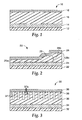
- exemplary multi-layered film sensor 10 comprises (optional) substrate layer 12, reflective layer 14, detection layer 16, and semi-reflective layer 18.
- the sensor films can be used for detecting the presence and/or concentration of an analyte or of a mixture of analytes.
- the analyte may be a gas (e.g., a vapor) or a liquid.
- the analyte can be a molecule, a macromolecule, a biomolecule, or a biomacromolecule.
- the analyte may be present in a gaseous medium (such as air) or liquid medium (such as water or other fluids).
- Typically the analyte is an organic material.
- the analyte is detected by a change in optical thickness of a polymer comprising a detection layer upon exposure to the analyte.
- the analyte passes through an outer semi-reflective layer and changes the optical thickness of the detection layer.
- the analyte is absorbed into at least a portion of the detection layer. Upon absorption, color changes (often vivid) can indicate the presence of the analyte.
- the change in optical thickness is typically observable in the visible light range and can be detected by the unaided human eye.
- sensors can be designed to show a change in optical thickness when subjected to other light sources such as UV, infrared, or near infrared.
- Various detection mechanisms can also be used. Examples of suitable detection mechanisms include spectrophotometers, fiber optic spectrophotometers, and photo-detectors, e.g., charge coupled devices (ccd), digital cameras, etc.
- the analyte is detected when its presence causes the delamination of the detection layer from an adjacent layer.
- delamination occurs when the analyte wets the interface of the detection layer and an adjacent layer, thereby reducing the interface adhesion.
- optical interference is destroyed and the sensor loses perceptible color.
- the presence of the analyte may also cause dewetting of one or more polymers within the detection layer from an adjacent layer. This process, which involves changes in the shape of the detection layer that reduce the interfacial area with adjacent layers, causes defects within the material which permanently change the optical properties of the sensor film.
- the substrate is optional, but when present it may comprise any suitable material capable of providing support for the colorimetric sensor. It may be flexible or non-flexible.
- the substrate material can be tailored to the application. Preferably, it is suitable to use in a vacuum deposition process.
- the reflective layer may comprise any material that can form a fully reflective or semi-reflective layer. It is preferable that the material is fully reflective at a thickness of about 20 to about 200 nm. Thinner layers can typically be used to make the reflective layer semi-reflective. Although the reflective layer is typically made to be more reflective than the semi-reflective layer, sometimes it is desirable to have the reflectivity of the reflective layer and semi-reflective layer be the same so a response to the presence of an analyte can be seen from either side of the sensor film.
- Suitable materials for the reflective layer include metals or semi-metals such as aluminum, chromium, gold, nickel, silicon, and silver.
- Other suitable materials that may be included in the reflective layer include metal oxides such as chromium oxide and titanium oxide.
- the reflective layer is at least about 90 % reflective (i.e., at least about 10 % transmissive), and in some embodiments, about 99 % reflective (i.e., about 1 % transmissive). In other exemplary embodiments of the present invention, the reflective layer is a semi-reflective layer, wherein the reflective layer is at least about 20 % reflective, such as about 20 to about 90 % reflective, or about 30 to about 70 % reflective.
- the reflective layer also acts as the substrate, providing support for the sensor.
- the reflective layer may be a substantially continuous layer or a discontinuous layer.
- the reflective layer may comprise one or more reflective layers.
- the reflective layer comprises a single reflective layer.
- the detection layer of the sensor comprises at least one polymer having an intrinsic micro porosity.
- the detection layer comprises at least one polymer whose optical thickness changes upon exposure to an analyte.
- the change in optical thickness can be caused by a dimensional change such as a change in physical thickness of the polymer due to swelling or shrinkage or a change in refractive index of the detection layer due to the presence or chemical reaction of the analyte.
- the detection layer may change from one color to another, from a color to no color, or from no color to a color.
- the detection layer may comprise one or more layers.
- the detection layer may also comprise two or more sub-layers.
- One or,more of the sub-layers may be discontinuous or patterned.
- the sub-layers typically comprise different polymeric materials and may absorb different analytes and/or may have different degrees of sensitivity to one or more analytes.
- the sub-layers may have a variety of configurations. For example, the sub-layers may be stacked to form a stack of two or more layers or may be positioned within the same layer in a side-by-side configuration.
- the detection layer may comprise a pattern so as to create colored images, words, or messages upon exposure to an analyte.
- a sublayer may be patterned by having one or more portions that are reactive to a particular analyte and one or more portions that are non-reactive to the same analyte.
- a pattern of reactive material may be deposited on a larger non-reactive sublayer. In this case, it is preferable to make the patterned layer very thin so that no difference in optical thickness is apparent until an analyte is absorbed.
- the patterning can provide easily identifiable warnings for a user upon exposure to an analyte.
- the thickness of the detection layer may be patterned, for example, as described in U.S. Patent No. 6,010,751 . This may be desirable when the sensor is designed so that the presence of an analyte causes the detection layer to swell or shrink, thereby making a pattern disappear (for example when a thinner portion swells to the same thickness as a thicker portion) or appear (for example, when an portion shrinks to a thinner thickness than an adjacent portion). Patterns may also be made to appear by starting with thinner and thicker regions that appear the same color initially, but, when exposed to one or more analytes, one or both of the thinner and thicker regions swell to give two different hues.
- the detection layer may comprise a blend of polymer components.
- the blend may be homogeneous or heterogeneous.
- a blend of polymer components in the detection layer can allow for a large number of analytes to be detected with the use of a relatively small sensor.
- the detection layer comprises at least two different polymeric components, wherein the polymeric components are (1) blended with one another, (2) within a given layer but not blended with one another (i.e., in a side-by-side configuration), (3) in a layer separate from one another (i.e., in a stack), or (4) any combination of (1) to (3).
- the detection layer may be porous.
- the detection layer may contain a continuous network of pores throughout its volume. This can boost the sensitivity of detection due to the increase in surface area exposed to an analyte and/or the propensity of pores to condense vaporous analytes.
- Porosity can be obtained by using porous materials such as foams made from high internal phase emulsions, such as those described in WO 01/21693 , to form the detection layer. Porosity may also be obtained via carbon dioxide foaming to create bi-continuous, nanoporous material ( see " Macromolecules", 2001, vol. 34, pp. 8792-8801 ), or by nanophase separation of polymer blends ( see “ Science", 1999, vol. 283, p. 520 ).
- the pore diameters need to be smaller than the wavelength of the light source used in the detection process.
- pores having an average pore size of 10 nm or less are desired within the detection layer.
- polymers having an intrinsic microporosity are used to form the detection layer.
- PIMs polymers having an intrinsic microporosity
- PIMs refer to non-network polymers that form microporous solids due to their highly rigid and contorted molecular structures. Because of their molecular structure, the PIMs are unable to fill space efficiently, resulting in a microporous structure (e.g., a structure that typically contains pores having an average pore size of less than about 2 nm).
- Suitable polymers of intrinsic microporosity include, but are not limited to, polymers disclosed in " Polymers of intrinsic microporosity (PIMs): robust, solution-processable, organic nanoporous materials," Budd et al., Chem. Commun., 2004, pp. 230-231 .
- One or more polymers within the detection layer may be at least partially crosslinked.
- Crosslinking may be desirable in some embodiments because it can increase mechanical stability and sensitivity to certain analytes.
- Crosslinking can be achieved by incorporating one or more multi-functional monomers into the detection layer, or by subjecting the detection layer to, e.g., electron beam or gamma ray treatment.
- crosslinking is done in the presence of a porogen, which may be subsequently extracted from the crosslinked system to yield a porous detection layer.
- Suitable porogens include, but are not limited to, inert organic molecules, such as normal alkanes (e.g., decane) or aromatics (e.g., benzene, toluene).
- the polymer or copolymer be hydrophobic. This will reduce the chance that water vapor (or liquid water) will cause a change in optical thickness of the polymer and interfere with the detection of an analyte, for example, in the detection of organic solvent vapors.
- polymeric materials suitable for the detection layer include, but are not limited to, polymers and copolymers (including block copolymers) prepared from classes of monomers including hydrophobic acrylates and methacrylates, difunctional monomers, vinyl monomers, hydrocarbon monomers (olefins), silane monomers, and fluorinated monomers.
- hydrophobic acrylates and methacrylates include, but are not limited to, n-alkyl(meth)acrylates having alkyl groups -C x H 2x CH 3 wherein x is from 1 to about 17, methyl(meth)acrylate, isodecyl(meth)acrylate, 2-ethylhexyl(meth)acrylate, cyclohexyl(meth)acrylate, n -decyl(meth)acrylate, n-butyl(meth)acrylate, isooctyl(meth)acrylate, isopropyl(meth)acrylate, lauryl(meth)acrylate, ethyl(meth)acrylate, adamantyl(meth)acrylate, t -butyl(meth)acrylate, 2-phenoxyethyt(meth)acrylate, isobornyl(meth)acrylate, and poly(dimethylsiloxane)mono(me
- multi-functional monomers include, but are not limited to, divinylbenzene, ethyleneglycol di(meth)acrylate, diethyleneglycol di(meth)acrylate, triethyleneglycol di(meth)acrylate, tetraethylene glycol di(meth)acrylate, tripropylene glycol di(meth)acrylate, polyethylene glycol di(meth)acrylate 1,6-hexanedioldi(meth)acrylate, trimethylol propane di(meth)acrylate, neopentyl glycol di(meth)acrylate, N,N-methylenebis(meth)acrylamide, poly(dimethylsiloxane)di(meth)acrylate, poly(ethyleneglycol)di(meth)acrylate, diacrylates such as those commercially available from UCB Chemicals under the trade designation "IRR 214", pentaerythritol tri- and tetra-acrylate, and trimethylol propane tri(meth)
- vinyl monomers include, but are not limited to, styrene, ⁇ -methylstyrene, vinylacetate, vinylbutyrate, vinylstearate, vinylchloride, and vinyl norbornene.
- hydrocarbon monomers examples include, but are not limited to, isobutylene, ethylene, propylene, butadiene, and norbornene.
- silane monomers include, but are not limited to, organohydrosilanes, alkoxysilanes, phenoxysilanes, and fluoroalkoxysilanes.
- fluorinated monomers include, but are not limited to, tetrafluoroethylene, vinylidene fluoride, hexafluoropropylene, and perfluoroalkyl(meth)acrylates.
- polymeric materials suitable for the detection layer include, but are not limited to, polymers and copolymers (including block copolymers) prepared from classes of monomers including hydroxylated monomers, acrylamides, anhydrides, aldehyde-functionalized monomers, amine or amine salt functionalized monomers, acid functionalized monomers, epoxide functionalized monomers, vinyl monomers, the multifunctional monomers listed above, and other polymers.
- hydroxylated monomers include, but are not limited to, hydroxyalkyl(meth)acrylates, hydroxyethyl(meth)acrylate, and hydroxymethyl(meth)acrylate.
- acrylamides and acrylonitriles include, but are not limited to, (meth)acrylamide, N-isopropyl (meth)acrylamide, N,N-dimethyl (meth)acrylamide, and (meth)acrylonitrile.
- anhydrides include, but are not limited to, (meth)acrylic anhydride and maleic anhydride.
- aldehyde-functionalized monomers examples include, but are not limited to, acrolein.
- amine or amine salt functionalized monomers include, but are not limited to, t-butylaminoethyl (meth)acrylate, diisopropylaminoethyl (meth)acrylate, dimethylaminoethyl (meth)acrylate, vinylpyridine, dimethylaminoethyl(meth)acrylate-methyl chloride salt, aminostyrene, 4-aminostyrene, and vinylimidazole.
- acid functionalized monomers include, but are not limited to, (meth)acrylic acid, carboxyethyl(meth)acrylate, (meth)acrylic acid-metal salts, styrene sulfonic acid, monomers commercially available from UCB Chemicals under the trade designation "EBECRYL 170" from UCB Chemicals, vinylphosphonic acid, and vinylsulfonic acid.
- epoxide functionalized monomers include, but are not limited to, glycidyl(meth)acrylate.
- vinyl monomers include, but are not limited to, N-vinylpyrrolidone, vinyldimethylazalactone (VDM), vinylidene chloride, vinylalcohol, and vinylphenol.
- polymers examples include, but are not limited to, poly(ethyleneoxide), poly(caprolactone), poly(sulfone), poly(ethyleneglycol), poly(urethanes), poly(carbonate), poly(ethyleneimine), poly(vinyl alcohol), poly(vinylphenol), ethyl cellulose, fluoropolyol, polyesters, polyamides, polyimides, and polyacetals.
- the polymer component(s) of the detection layer may also have appropriate functional groups or molecular receptors incorporated to detect specific analytes.
- acid-functionalized polymers such as poly(acrylic acid), enable detection of organic bases such as ammonia gas.
- Suitable molecular receptors include, but are not limited to, calixarenes, cyclodextrins, dendritic polymers, carbon nanotubes, azacrowns, crown ethers, anion chelating agents containing Lewis acid functionality, organometallic metal complexes, porphyrins, metalloporphyrins, peptides, glycopeptides, proteins, antibodies, enzymes, oligonucleotides, and nucleic acids.
- the detection layer comprises one or more inorganic materials in combination with one or more of the above-described polymeric materials.
- the detection layer comprises one or more inorganic materials in combination with one or more of the above-described polymeric materials.
- the inorganic materials may be present as a distinct layer within the detection layer or may be intermixed with polymeric material to form a single layer. Further, the inorganic materials may be present as a distinct layer within the detection layer separate from one or more polymeric layers (i.e., in a stack of polymeric layers and inorganic layers) or may be within a single layer along with polymeric material but not intermixed with the polymeric material (i.e., a side-by-side configuration having a distinct section of inorganic material and a distinct portion of polymeric material).
- Suitable inorganic materials for use in the detection layer include, but are not limited to, transparent and porous metal oxides, nitrides, and oxynitrides of appropriate thickness for producing color by optical interference.
- suitable inorganic materials include, but are not limited to, silicon oxides, silicon nitrides, silicon oxynitrides, aluminum oxides, titanium oxides, titanium nitride, titanium oxynitride, tin oxides, zirconium oxides, and combinations thereof.
- Other inorganic materials, such as zeolites are also suitable for use in the detection layer.
- the inorganic material is a porous material as defined above.
- inorganic materials are used as "analyte sorptive materials" or “analyte reactive materials” within the detection layer.
- inorganic materials such as those described above, may be used alone or may be used as a base substrate having analyte-reactive or analyte-sorptive groups bonded thereto.
- particulate metal oxides, nitrides, and/or oxynitrides having an organosilane compound bonded thereto may be distributed throughout the detection layer.
- receptor molecules such as peptides or antibodies, may potentially be covalently linked to the polymer.
- biosensors for selective detection of bacteria, proteins, ions, etc. could be fabricated.
- the detection layer can have any desired overall thickness. Desirably, the detection layer has an overall thickness of more than about 50 nm, such as in the range of about 100 to about 1000 nm. In one embodiment of the present invention, the detection layer has a layer thickness that is substantially the same throughout the detection layer. See, for example, detection layer 16 of Fig. 1 . In other embodiments of the present invention, the detection layer has a layer thickness that varies from a first location within the detection layer to one or more other locations within the detection layer. In either case, the semi-reflective layer applied over the detection layer may be applied so as to conform to the thickness variations in the detection layer.
- sensor 20 comprises (optional) substrate layer 22, reflective layer 24, detection layer 26, and semi-reflective layer 28.
- Detection layer 26 has a first thickness, t 26a , at first location 26a, a second thickness, t 26b , at second location 26b, and a third thickness, t 26c , at third location 26c.
- the layer thickness of detection layer 26 varies throughout detection layer 26, the thickness of semi-reflective layer 28 remains substantially constant.
- the detection layer comprises one or more "wells" positioned within the detection layer.
- the term "wells” is used to describe holes, grooves, channels, or any other voids (other than pores) within the detection layer. Unlike pores, wells do not form a continuous network throughout the detection layer volume. Typically, wells extend from an upper surface of the detection layer (i.e., below the semi-reflective layer) into the detection layer a given depth. Wells typically have at least one dimension (i.e., length, width, or diameter) of less than about 10 nm; however, any well size may be used in the present invention.
- the wells have at least one dimension (i.e., length, width, or diameter) ranging from about 1.0 to about 10 nm, more desirably, about 5 nm. In some embodiments of the present invention, the wells have at least one dimension (e.g., width) ranging from about 1.0 to about 10 nm, and at least one other dimension (e.g., length) much greater than 5 nm, such as a dimension ranging from greater than 10 nm to the width of the detection layer.
- An exemplary sensor of the present invention containing wells within the detection layer is shown in Fig. 3 .
- exemplary multi-layered film sensor 30 comprises (optional) substrate layer 32, reflective layer 34, detection layer 36 having wells 37 therein, and semi-reflective layer 38 over detection layer 36 and wells 37.
- detection layer 36 has an increased surface area due to surface areas 37a along inner surfaces of wells 37.
- the degree of increased surface area within detection layer 36 may be controlled by varying one or more of the following parameters: the number of wells 37 per given area, the depth of each well 37, and the volumetric size of each well 37.
- Wells when present, may be present as random voids within the detection layer or in the form of a pattern distributed within the detection layer, wherein the wells extend a desired depth into the detection layer.
- the wells may be provided using a variety of techniques.
- One suitable method for providing wells within the detection layer comprises an etching method as described in Example 10 below.
- a reflective layer is first coated onto a temporary or permanent carrier.
- a polymeric detection layer is then coated onto the reflective layer.
- a metal, such as Cr is coated onto the detection layer in "island" form (i.e., a pattern of metal islands and uncoated areas).
- the size and density of the islands on the detection layer may be controlled by the placement of a screen between the metal (i.e., Cr) source and the detection layer. Then, oxygen plasma in Reactive Ion Etch (RIE) mode is used to etch the detection layer in uncoated areas.
- RIE Reactive Ion Etch
- the metal (e.g., Cr) islands serve as an etch mask, and are converted to a transparent oxide, such as CrO x , during the etching step (see, for example, layer 39 in Fig. 3 ).
- the above-described exemplary etching process produces nanometer-dimensioned wells between the transparent oxide islands.
- the transparent oxide islands are uniformly dispersed over an upper surface of the detection layer and have at least one dimension (i.e., length, width, or diameter) of less than about 100 nm; however, any transparent oxide island size, shape, and density may be used in the present invention.
- Wells 37 may extend into detection layer 36 at any depth as desired for a given application. As shown in Fig. 3 , wells 37 may extend into detection layer 36 and end at some point within detection layer 36. In other embodiments, wells 37 may extend through detection layer 36 to reflective layer 34 (see Fig. 3 ) .
- a semi-transparent layer may be coated over the transparent oxide islands and wells, such as semi-transparent layer 38 shown in Fig. 3 .
- color-shifting interference results in the appearance of a single uniform color, which varies with a given viewing angle.
- the transparent oxide islands i.e., layer 39 shown in Fig. 3
- the transparent oxide islands may be removed prior to applying the semi-transparent layer over the detection layer "islands" and wells positioned between the "islands.”
- the semi-reflective layer may comprise any material that can form a permeable, semi-reflective layer and has a different index of refraction than the detection layer. In most embodiments, it is preferable that the material is semi-reflective at a thickness of about 5 nm because at this thickness most analytes will be able to permeate through this layer to the detection layer. Desired thicknesses will depend on the material used to form the layer, the analyte to be detected, and the medium that will carry the analyte.
- Suitable materials include metals and semi-metals such as aluminum, chromium, gold, nickel, silicon, and silver.
- Other suitable materials that may be included in the semi-reflective layer include oxides such as aluminum oxide, titanium oxide, and chromium oxide.
- the semi-reflective layer may be a substantially continuous layer or a discontinuous layer. Further, like the reflective layer, the semi-reflective layer may comprise one or more semi-reflective layers. Desirably, the semi-reflective layer comprises a single semi-reflective layer, which is either substantially continuous or discontinuous.
- the semi-reflective layer is a substantially continuous layer.
- the construction and composition of the semi-reflective layer may be substantially consistent across an upper surface of and throughout the semi-reflective layer.
- the construction and/or composition of the semi-reflective layer may vary across an upper surface of and throughout the semi-reflective layer.
- the semi-reflective layer may have a differential permeability such that the semi-reflective layer has higher analyte permeability for a given analyte at a first location on an upper surface of the semi-reflective layer and lower analyte permeability for the same analyte at a second location on the upper surface.
- the first and second locations on the upper surface of the semi-reflective layer may be randomly positioned relative to one another, or may form a pattern on the upper surface.
- the substantially continuous semi-reflective layer may also have a pattern therein wherein first regions of the semi-reflective layer have a greater light reflectance than second regions of the semi-reflective layer.
- the first and second regions on the semi-reflective layer may form a pattern on the upper surface of and within the semi-reflective layer.
- a patterned semi-reflective layer may comprise a pattern so as to create colored images, words, or messages upon exposure of the underlying detection layer to an analyte.
- the semi-reflective layer can provide easily identifiable warnings for a user upon exposure to an analyte.
- any number of methods may be used to alter the permeability of the semi-reflective layer and/or create a pattern on and within the semi-reflective layer. Suitable methods include, but are not limited to, spatially controlling the deposition conditions of the semi-reflective layer to vary the thickness or density of the semi-reflective layer. For example, a mask can be placed between the deposition source and the substrate such that the thickness of deposited semi-reflective layer varies from a first location to a second location on an upper surface.
- the differential permeability and/or creation of a pattern on and within the semi-reflective layer can also be produced by post-treatment of the semi-reflective layer with localized energy inputs such as laser treatment to change the microstructure of the semi-reflective layer.
- any of the above-mentioned methods may be used to create one or more patterns on the semi-reflective layer.
- the choice of a given pattern or patterns may depend on a number of factors including, but not limited to, the analyte or analytes of interest, the semi-reflective material or materials used, the message, if any, displayed to a user, or a combination thereof.
- Exemplary multi-layered films of the present invention having a substantially continuous semi-reflective layer are shown in Figs. 1-3 .
- the multi-layered film sensor comprises a substantially continuous semi-reflective layer over a detection layer, wherein the detection layer has an increased surface area for potentially enhanced detection of an analyte due the presence of one or more wells within the detection layer (see Fig. 3 ).
- the substantially continuous semi-reflective layer positioned over the detection layer containing wells is a single layer of semi-reflective material.
- the semi-reflective layer is a discontinuous layer.
- the composition of the semi-reflective layer may be substantially consistent across the semi-reflective layer; however, areas separate the semi-reflective layer into two or more discontinuous regions.
- the discontinuous semi-reflective layer may comprise any pattern of semi-reflective islands within a "sea" of exposed areas (i.e., the detection layer is exposed). The size and density of semi-reflective islands on the detection layer may vary as desired, and may be uniformly dispersed or non-uniformly dispersed over an upper surface of the detection layer.
- the semi-reflective islands are uniformly dispersed over an upper surface of the detection layer and have at least one dimension (i.e., length, width, or diameter) of at least about 1.0 micron ( ⁇ m), desirably, from about 10.0 to about 100 ⁇ m; however, any semi-reflective island size, shape, and density may be used in the present invention.
- the exposed areas typically have at least one dimension (i.e., length, width, or diameter) ranging from about 1.0 to about 100 ⁇ m; however, the exposed areas may have any dimensions in the present invention.
- Exemplary multi-layered film sensor 40 comprises (optional) substrate layer 42, reflective layer 44, detection layer 46, and discontinuous semi-reflective layer 48 over detection layer 46.
- discontinuous semi-reflective layer 48 comprises semi-reflective islands 48a and exposed areas 49 within a given plane above detection layer 46. Exposed areas 49 provide immediate access for an analyte to detection layer 46 without the need to permeating through a semi-reflective material.
- the degree of exposure of detection layer 46 may be controlled by varying one or more of the following parameters: the number of semi-reflective islands 48a per given area, and the size of each semi-reflective island 48a.
- One suitable method for providing a discontinuous semi-reflective layer over a detection layer comprises laser ablation method as described in Example 11 below. Portions of the semi-reflective layer may be removed by exposing the portions to a laser as described in U.S. Patents Nos. 6,180,318 and 6,396,616 assigned to 3M Innovative Properties Company (St. Paul, MN).
- Another exemplary method that could be used to produce a discontinuous semi-reflective layer is a photo-imaging method.
- the discontinuous semi-reflective layer comprises a number of semi-reflective islands uniformly dispersed over an upper surface of the detection layer, wherein each semi-reflective island has an upper surface area in the shape of a square or circle having a length, width, or diameter of at least about 1.0 ⁇ m, more desirably, from about 10.0 to about 100 ⁇ m. It should be understood that each semi-reflective island may have an upper surface area in a variety of shapes including, but not limited to, triangular, rectangular, star-shaped, diamond-shaped, etc., and one or more dimensions of at least about 1.0 ⁇ m, more desirably, from about 10.0 to about 100 ⁇ m.
- each semi-reflective island may be either permeable or impermeable to one or more analytes.
- the colorimetric sensor allows one or more analytes to contact the detection layer directly through exposed areas, as well as indirectly through the semi-reflective islands.
- the resulting structure comprises an array of multi-layered film islands (e.g., square islands having 100 ⁇ m sides within a grid of exposed areas having a width of about 10 ⁇ m) having the same detection layer composition and semi-reflective layer composition.
- each island can be either permeable or impermeable to one or more analytes.
- the multilayer structures enable penetration of an analyte into the detection layer from the sides of the detection layer, as well as from the top of the detection layer.
- the size, shape and density of multi-layered film islands within the resulting structure may vary similarly to the semi-reflective islands described above.
- each multi-layered film island has one or more dimensions of at least about 1 ⁇ m such as about 10.0 to about 100 ⁇ m.
- multi-layered film islands may also be formed by depositing islands of detection layer material onto a reflective layer and then depositing a semi-reflective layer on top of each detection layer island.
- Various printing techniques including, but not limited to, ink-jet printing and contact printing, may be used to deposit the detection layer in island or patterned form onto a reflective layer.
- the discontinuous semi-reflective layer comprises a single layer of semi-reflective islands over an upper surface of a detection layer, wherein the detection layer comprises at least one inorganic component.
- the discontinuous semi-reflective layer comprises a single layer of semi-reflective islands over an upper surface of a detection layer, wherein the detection layer comprises at least one inorganic component in combination with at least one polymer component.
- the discontinuous semi-reflective layer comprises a single layer of semi-reflective islands over an upper surface of a detection layer, wherein the detection layer comprises at least two different polymeric components, wherein the polymeric components are (1) blended with one another, (2) within a given layer but not blended with one another, (3) in a layer separate from one another, or (4) any combination of (1) to (3).
- the sensor film may comprise additional layers between any of the previously described layers, as long as the additional layer (or layers) does not interfere with the optics of the sensor film. Additional layers could include tie layers, structural layers, etc.
- the sensor film may also include additional layers above the semi-reflective layer. Suitable additional layers that may at least partially cover the semi-reflective layer include, but are not limited to, a transparent layer or laminate, and a masking layer to temporarily or permanently shield a portion of the semi-reflective layer from exposure to one or more analytes.
- the additional layers may be applied directly onto the semi-reflective layer or may be temporarily or permanently bonded to the semi-reflective layer via a tie layer or other adhesive layer. If necessary, an outer surface of the semi-reflective layer may be treated (e.g., chemically etched or primed, electrical discharge treatment, etc.) to enhance the bond to additional layers.
- a masking layer is provided over the semi-reflective layer in the form of a pattern.
- the colorimetric sensor upon exposure to an analyte, displays a signal in the form of a pattern (i.e., a reverse pattern of the masking layer on the semi-reflective layer).
- the signal pattern may have any desired configuration including, but not limited to, shapes, letters, words, a specific message to the user, safety instructions to the user, a company logo, etc.
- the multi-layered films of the present invention may be used alone or may be part of a device for detecting the presence and/or concentration of one or more analytes.
- the multi-layered film sensor is at least partially enclosed by a housing.
- the housing desirably comprises at least one opening positioned above the semi-reflective layer so that the semi-reflective layer is viewable through the at least one opening.
- the housing comprises at least one opening, wherein the at least one opening provides a restricted view of an upper surface of the semi-reflective layer so as to minimize any potential change in the viewable color of the sensor (and confusion of the user as to the sensor reading) due to the angle of view.
- the restricted view allows a view of the upper surface of the semi-reflective layer within an angle of ⁇ 30°, more desirably, ⁇ 15° from a normal view (i.e., a view from a position perpendicular to the outer surface of the semi-reflective layer).
- the housing may also be used to constrain the multi-layered film sensor of the present invention so that the film is in an arched or cylindrical shape. Such a configuration allows a user to view the sensor from a larger range of viewing angles with minimal shift in color.
- the multi-layered film sensors of the present invention may possess a substantially continuous semi-reflective layer or a discontinuous semi-reflective layer.
- the colorimetric sensor comprises a substantially continuous reflective layer; a detection layer over the reflective layer, wherein the detection layer comprises (i) at least one polymer component having an intrinsic micro porosity, (ii) at least one inorganic component, or (iii) both (i) and (ii); and a substantially continuous semi-reflective layer over the detection layer, wherein the semi-reflective layer has an index of refraction different from the index of refraction of the detection layer and is permeable to a given analyte.
- the substantially continuous reflective layer, the substantially continuous semi-reflective layer, or both comprise a single layer of reflective or semi-reflective material to minimize the thickness of either or both layers so that one or more analytes can permeate either or both layers.
- the multi-layered films can be created via methods such as the process described, e.g., in U.S. Patent 5,877,895 .
- the reflective and semi-reflective layers may also be made by standard vapor coating techniques such as evaporation, sputtering, chemical vapor deposition (CVD), plasma deposition, or flame deposition. Another method for making the reflective and semi-reflective layers is plating out of solution.
- the film sensors may be used in a system comprising the sensor, a light source, and, optionally, a means of monitoring the sensor for a change of color.
- the light source can be a natural or artificial light source.
- the monitoring can be done in a variety of ways. It could be done visually, with a photo-detector, or by other suitable means.
- the analyte may be present in a vapor or liquid medium.
- an analyte may be present in the atmosphere or in a liquid solvent.
- at least a portion of the analyte permeates through the semi-reflective layer of the film sensor to interact with the detection layer.
- Two or more film sensors may be used together to form an array.
- the array may be in any suitable configuration.
- an array may comprise two or more sensors side by side, or sensors may be attached to, or constructed on, opposite sides of a substrate.
- the sensors within a given array may be of the same type or may be different.
- Arrays of multi-layered film sensors would be useful for identification of analytes, based upon their unique response signatures from the array in aggregate, as opposed to only detecting the presence of a chemical agent.
- Each of exemplary arrays 50-55 comprises a base layer 57 and multi-layered film stacks 58 on an upper surface of base layer 57.
- Base layer 57 may be a substrate layer or a reflective layer as described above.
- Multi-layered film stacks 58 within a given array may have identical or different chemical compositions.
- two or more multi-layered film stacks 58 within a given array may have (i) different detection layer chemistries (and/or receptor types, e.g.
- calixarenes peptides
- detection layer pore size distributions peptides
- detection layer thicknesses within a given stack or any combination of (i) to (iii), so as to detect the presence and/or concentration of one or more analytes in a given sample medium.
- the array comprising two or more colorimetric sensors, wherein each colorimetric sensor in the array comprises a colorimetric sensor according to claim 1.
- each colorimetric sensor in the array shares a common reflective layer.
- the array comprises two or more colorimetric sensors, wherein each colorimetric sensor in the array (a) shares a common reflective layer and (b) comprises a multi-layered film island comprising a stack of layers including (i) a detection layer with a detection layer composition and (ii) a semi-reflective layer with a semi-reflective layer composition.
- the detection layer composition is similar for each colorimetric sensor in the array and the semi-reflective composition is similar for each colorimetric sensor in the array.
- sensor arrays may be configured as one or more discrete sensor elements in a uniformly distributed manner (e.g., array 51), in a non-uniform manner (e.g., array 55), side by side (bar gauge type, etc.) (e.g., array 52), or any other configuration.
- the film sensors of the present invention have many useful applications. They can be used, e.g., to detect a wide range of organic vapors.
- the sensors may be used to detect the presence and/or concentration of a given analyte within a solution or gas.
- Sensor arrays may be used to detect the presence and/or concentration of one or more analytes within a solution or gas.
- the multi-layered film sensors provide an overall color pattern to a user based on the interaction of a liquid or gas medium with the array, rather than on the interaction of a liquid or gas medium with a single sensor element.
- the multi-layered film sensors of the present invention Prior to use, are substantially free of an analyte to be detected.
- the "unexposed" multi-layered film sensor prior to use typically either (i) displays a first color or (ii) is colorless when viewed through the semi-reflective layer. Upon exposure to one or more analytes to be detected, the "unexposed" multi-layered film sensor converts to an analyte-containing colorimetric sensor.
- the analyte-containing colorimetric sensor either (i) displays a second color that is different from the first color, (ii) undergoes a color change from a first color to a colorless condition, or (iii) undergoes a color change from a colorless condition to a color-containing condition.
- the multi-layered film sensor of the present invention may contain or be substantially free of biological material between the reflective layer and the semi-reflective layer.
- biological material is used to encompass molecular receptors such as peptides, glycopeptides, proteins, antibodies, enzymes, oligonucleotides, and nucleic acids.
- the method detects the presence or absence of an analyte, wherein the method comprises providing a colorimetric sensor (or array of sensors), providing a light source, contacting the sensor (or array of sensors) with a medium that may contain an analyte, and monitoring the sensor (or array of sensors) for a change in optical properties.
- the medium may be a liquid or a gas.
- the one or more analytes may permeate through the semi-reflective layer, the reflective layer, or both layers.
- the sensor film samples were viewed from an angle normal to the surface of the film. Other viewing angles may be used. The color observed can vary depending on the angle of observation.
- a multi-layered colorimetric sensor film was produced via the deposition method described in U.S. Patent No. 5,877,895 .
- An aluminum reflective layer (100 nm) and polymeric detection layer (500 nm) were sequentially deposited upon a polyester substrate layer (50 ⁇ m) in a single pass (15.24 m/min) through a vacuum web system.
- the aluminum reflective layer was thermally evaporated by feeding 0.1587 cm diameter aluminum wire (Alcoa stock number 1199, Pittsburgh, PA) onto an electrically heated (7V, 1250 amp) evaporation bar at a feed rate of 225 mm/min.
- the polymeric detection layer (500 nm) was deposited followed by an electron beam cure of 6.9 W-Sec.
- the monomer composition was a 48.5/48.5/3 by weight mixture of lauryl acrylate (available from Sartomer, Exton, PA) /IRR214 (a proprietary hydrocarbon diacrylate, available from UCB Chemicals, Drogenbos, Belgium)/EBECRYL 170 (a phosphoric acid monoacrylate compound also available from UCB Chemicals).
- Chromium (Academy Precision Materials, Albuquerque, NM) was then sputtered (2.95 W/cm2 DC power at 2 mTorr Argon pressure), in a subsequent pass (15.24 m/min) through the vacuum web system, onto the cured detection layer, to give a 5 nm thick outer layer.
- the multi-layer sensor film had a green hue.
- Sections of the multi-layered film (2.54 cm square) were affixed on glass slides and exposed for one minute to saturated vapors of various organic solvents in sealed jars. Within each jar, the multi-layered film was suspended within the headspace above the neat liquid analyte. As shown in Table 1, the exposures resulted in vivid, visually detectable color changes. In each case, the color changes were reversible upon removal from the solvent vapor within tens of seconds, restoring the original green hue. Responses were qualitatively reproducible, as repeat exposures produced the same color changes.
- Visible reflectance spectra were taken of the multi-layered films before and after exposure to a range of solvent vapors.
- Film sections (2.54 cm square, from Example 1) were affixed on glass slides and exposed to saturated organic vapors within sealed jars. Once equilibrated, the exposed films were removed and covered immediately with glass cover slides to prevent vapor desorption. Reflectance spectra of the exposed materials were then taken using a diffuse reflectance UV-VIS spectrometer. For all organic vapors tested, substantial red-shifting of the reflectance maxima were observed upon analyte exposure. The reflectance maximum centered at 524 nm (before exposure), for instance, exhibits shifts to higher wavelengths (red shifts).
- the magnitudes of the shifts ranged from 22 nm (acetonitrile) to 116 nm (methylene chloride), as shown in Table 2.
- This example shows that the multi-layered colorimetric sensor films respond to organic vapors, exhibiting colorimetric shifts for halocarbons, arenes, alcohols, ketones, nitriles and ethers. No shift was observed in the reflectance spectra on exposure to saturated water vapor. Even upon submerging films in liquid water, no color change was observed.
- sensor film made as described in Example 1, was exposed to analytes at a range of concentrations using a simple flow-through setup. Concentrations (as determined by partial pressures) were controlled by bath temperatures. Air was bubbled through neat liquid analytes, which were chilled using cold temperature baths to control the vapor pressure. Mixtures of solid carbon dioxide (dry ice) and 3-heptanone or ethylene glycol gave bath temperatures of -38°C and -15°C respectively. An ice water bath was used to give temperatures of 0°C. Vapor pressures for each analyte were calculated at these temperatures using data from the Handbook of Vapor Pressure (Yaws, C. L.
- Table 3 presents the responses as a function of concentration, with “green” indicating the unexposed film color, “pink” indicating response for saturated vapors, and “yellow” indicating an intermediate response. The results indicate the ability to determine analyte concentration, as well as the qualitative presence of the vapor using the colorimetric sensor films.
- Sensor film from Example 1 was used to detect organic compounds in water. Submersion of the film within a solution of tetrahydrofuran (THF) in water (5% by volume) yielded a visual change in color from green to yellow. Submersion into a solution of acetone in water (25% by volume) produced a visible change in color from green to yellow-green.
- THF tetrahydrofuran
- Two multi-layered sensor films were prepared via spin-coating of the detection layers.
- the structures were the same, except for the polymer detection layers.
- an aluminum reflective layer 100 nm was deposited by electron beam evaporation (2.5 nm/sec evaporation rate) in a batch system vacuum coater onto a 50 ⁇ m polyester substrate layer.
- Poly(styrene) and poly(methylmethacrylate) detection layers were each deposited onto one of the aluminum-coated substrates via spin-coating.
- the polymers were coated via toluene solutions at concentrations of 5% (w/w) and 9.4% (w/w) respectively.
- the spin-coating was carried out at 3500 rpm for 25 seconds.
- the resulting polymer thicknesses were 260 nm (poly(styrene)) and 500 nm (poly(methylmethacrylate)). Chromium layers (5 nm) were then deposited onto each polymeric surface via sputtering conditions identical to those in Example 1, to complete the multi-layered sensor film constructions. Exposure of the sensor films to saturated chloroform vapor yielded reversible color shifts from purple to blue (poly(styrene)) and from pink to light green (poly(methylmethacrylate)). Exposure of the films to toluene vapor caused a permanent loss of interference-based color, as indicated by the failure of the film to recover its original color upon removal from the analyte.
- TEM Transmission electron microscopy
- Two different multi-layered films were constructed having the same general structure and composition as that described in Example 1 except that the detection layer thickness for Sample 6A was 500 nm, while the thickness was 650 nm for Sample 6B. Both films contained detection layers made via polymerization of lauryl acrylate/IRR214/EB170 mixtures, as in Example 1. Responses of the two films to a series of vapors are shown in Table 4. While neither individual sensor can identify every analyte (i.e., 6A does not distinguish between toluene and acetone and 6B does not distinguish between acetonitrile and acetone), the combined responses from both sensors are unique to each species tested.
- Each polymeric sample was spincoated onto the aluminum sides of separate 1.5 inch X 1.5 inch (3.8 cm X 3.8 cm) sections of the a
- the spin-coating was carried out at 3000 rpm for 1 minute, producing polymer film thicknesses of 500, 270, 250, and 290 nm, respectively. Chromium layers (5 nm) were then deposited onto each polymeric surface via sputtering conditions identical to those in Example 1 to complete each multi-layered film construction.
- Samples 6A and 6B described in Example 6 were also used within the six-membered sensor array. Sections of each film were fixed on glass slides and then exposed to saturated vapors in sealed jars. The initial colors and colors upon vapor exposure are noted in Table 5.
- Multi-layered films were constructed similarly to the method described in Example 5.
- Aluminized polyester was prepared via evaporative coating of a 100 nm Al layer onto the polyester substrate.
- a 10% (mass/volume) solution of poly(vinylalcohol) (Aldrich, 89% hydrolyzed, 85,000-141,000 MW) in water was spincoated (3000 rpm, 1 min.) onto a section of the aluminized polyester fixed on a glass slide.
- the three layer film was then sputter coated with a 5 nm thickness of Cr to complete the stack.
- a multilayer film containing a poly(vinylpyrrolidone) (Aldrich, 55,000 MW) detection layer was made in analogous fashion by spincoating from a 10% (mass/volume) ethanol solution.
- Example 8 The poly(vinylalcohol) containing multi-layered film described in Example 8 was covered with patterned sections of 810 SCOTCH BRAND MAGIC tape from 3M Company, which were cut against a printed 3M logo template.
- the laminated multilayer film exhibited color change upon exposure to moisture. Color change occurred only in the unlaminated regions, causing the 3M logo to emerge.
- Multi-layered films were constructed similarly to the method described in Example 1 except "Cr islands" were applied to the polymeric detection layer instead of a continuous Cr layer.
- a screen was placed between the Cr source and the polymeric detection layer, and the Cr was then sputtered onto the screen and cured detection layer to provide Cr islands having a thickness of 5 nm, and a square shape having length of 100 nm.
- An oxygen plasma in RIE mode, was used to etch the polymer between the Cr islands. During the etching process, the Cr islands were converted to a transparent CrO x coating.
- the resulting "wells" within the detection layer had a width of about 5 nm, and a depth of about 100 nm.
- a semi-reflective layer of Cr was then sputter coated as in Example 1 to provide a substantially continuous semi-reflective layer having a thickness of 5 nm.
- Multi-layered films were constructed similarly to the method described in Example 1. After applying the substantially continuous semi-reflective Cr layer, portions of the semi-reflective Cr layer were removed using a laser ablation procedure as described in U.S. Patent No. 6,180,318 resulting in square shaped islands having a length of 100 ⁇ m. The dimensions of semi-transparent area removed were visible (i.e., the wells had a width of about 10 ⁇ m), but sufficiently small so as to produce a color change when exposed to an analyte.
- Multi-layered films were constructed similarly to the method described in Example 11 except that portions of the detection layer were also removed using the laser ablation procedure.
- the resulting multi-layered film islands had a square shape with a length of 100 ⁇ m.
- the islands were separated by wells having a width of 10 ⁇ m, and a depth of about 505 nm.
Landscapes
- Life Sciences & Earth Sciences (AREA)
- Health & Medical Sciences (AREA)
- Physics & Mathematics (AREA)
- Chemical & Material Sciences (AREA)
- Immunology (AREA)
- General Physics & Mathematics (AREA)
- Analytical Chemistry (AREA)
- Biochemistry (AREA)
- General Health & Medical Sciences (AREA)
- Pathology (AREA)
- Engineering & Computer Science (AREA)
- Molecular Biology (AREA)
- Hematology (AREA)
- Urology & Nephrology (AREA)
- Biomedical Technology (AREA)
- Chemical Kinetics & Catalysis (AREA)
- Plasma & Fusion (AREA)
- Spectroscopy & Molecular Physics (AREA)
- Food Science & Technology (AREA)
- Cell Biology (AREA)
- Microbiology (AREA)
- Biophysics (AREA)
- Biotechnology (AREA)
- Medicinal Chemistry (AREA)
- Investigating Or Analysing Materials By Optical Means (AREA)
- Investigating Or Analysing Materials By The Use Of Chemical Reactions (AREA)
- Push-Button Switches (AREA)
- Mechanical Pencils And Projecting And Retracting Systems Therefor, And Multi-System Writing Instruments (AREA)
- Spectrometry And Color Measurement (AREA)
- Optical Elements Other Than Lenses (AREA)
- Optical Measuring Cells (AREA)
Priority Applications (1)
| Application Number | Priority Date | Filing Date | Title |
|---|---|---|---|
| PL05779476T PL1728067T3 (pl) | 2004-03-24 | 2005-02-22 | Czujnik kolorymetryczny |
Applications Claiming Priority (2)
| Application Number | Priority Date | Filing Date | Title |
|---|---|---|---|
| US10/807,655 US7449146B2 (en) | 2002-09-30 | 2004-03-24 | Colorimetric sensor |
| PCT/US2005/005468 WO2005111588A1 (en) | 2004-03-24 | 2005-02-22 | Colorimetric sensor |
Publications (2)
| Publication Number | Publication Date |
|---|---|
| EP1728067A1 EP1728067A1 (en) | 2006-12-06 |
| EP1728067B1 true EP1728067B1 (en) | 2011-01-19 |
Family
ID=35107071
Family Applications (1)
| Application Number | Title | Priority Date | Filing Date |
|---|---|---|---|
| EP05779476A Expired - Lifetime EP1728067B1 (en) | 2004-03-24 | 2005-02-22 | Colorimetric sensor |
Country Status (13)
| Country | Link |
|---|---|
| US (1) | US7449146B2 (enExample) |
| EP (1) | EP1728067B1 (enExample) |
| JP (1) | JP4819793B2 (enExample) |
| KR (1) | KR101194470B1 (enExample) |
| CN (1) | CN1957246B (enExample) |
| AT (1) | ATE496290T1 (enExample) |
| AU (1) | AU2005242832B2 (enExample) |
| BR (1) | BRPI0509132B8 (enExample) |
| CA (1) | CA2560750A1 (enExample) |
| DE (1) | DE602005025984D1 (enExample) |
| PL (1) | PL1728067T3 (enExample) |
| RU (1) | RU2360232C2 (enExample) |
| WO (1) | WO2005111588A1 (enExample) |
Families Citing this family (87)
| Publication number | Priority date | Publication date | Assignee | Title |
|---|---|---|---|---|
| US20050171449A1 (en) * | 2000-03-21 | 2005-08-04 | Suslick Kenneth S. | Method and apparatus for detecting ammonia from exhaled breath |
| US20040062682A1 (en) * | 2002-09-30 | 2004-04-01 | Rakow Neal Anthony | Colorimetric sensor |
| US7449146B2 (en) | 2002-09-30 | 2008-11-11 | 3M Innovative Properties Company | Colorimetric sensor |
| US20050221279A1 (en) * | 2004-04-05 | 2005-10-06 | The Regents Of The University Of California | Method for creating chemical sensors using contact-based microdispensing technology |
| US7939022B2 (en) * | 2004-08-05 | 2011-05-10 | Avago Technologies General Ip (Singapore) Pte. Ltd. | Integration of colorimetric transducers and detector |
| US7080939B1 (en) * | 2004-10-04 | 2006-07-25 | The United States Of America As Represented By The Secretary Of The Air Force | Polymeric thermal history sensor |
| US8293340B2 (en) * | 2005-12-21 | 2012-10-23 | 3M Innovative Properties Company | Plasma deposited microporous analyte detection layer |
| US7556774B2 (en) * | 2005-12-21 | 2009-07-07 | 3M Innovative Properties Company | Optochemical sensor and method of making the same |
| WO2008030262A1 (en) * | 2005-12-29 | 2008-03-13 | 3M Innovative Properties Company | Method for atomizing material for coating processes |
| EP2035813B1 (en) * | 2006-06-16 | 2012-06-06 | Sony DADC Austria AG | Optical sensor and method for indicating the age or quality of a natural product |
| JP4681052B2 (ja) * | 2006-06-26 | 2011-05-11 | 日本電信電話株式会社 | フローセルおよびその製造方法 |
| US7767143B2 (en) * | 2006-06-27 | 2010-08-03 | 3M Innovative Properties Company | Colorimetric sensors |
| US8067110B2 (en) * | 2006-09-11 | 2011-11-29 | 3M Innovative Properties Company | Organic vapor sorbent protective device with thin-film indicator |
| US7906223B2 (en) * | 2006-09-11 | 2011-03-15 | 3M Innovative Properties Company | Permeable nanoparticle reflector |
| US7704751B2 (en) * | 2006-09-18 | 2010-04-27 | 3M Innovative Properties Company | Polymeric fluorescent chemical sensor |
| US8120854B2 (en) | 2006-12-28 | 2012-02-21 | 3M Innovative Properties Company | Interference films having acrylamide layer and method of making same |
| US8137979B2 (en) * | 2007-06-25 | 2012-03-20 | Qinetiq Limited | Preconcentrator device |
| CA2690368A1 (en) * | 2007-06-25 | 2008-12-31 | Qinetiq Limited | Heater suitable for use in a preconcentrator device |
| EP2205965B1 (en) * | 2007-10-05 | 2017-11-01 | 3M Innovative Properties Company | Organic chemical sensor comprising microporous polymer, and method of use |
| US20110157588A1 (en) * | 2007-12-13 | 2011-06-30 | Universität Wien | Device comprising two reflecting layers and a polymer layer for analyzing the age and/or quality of a natural product |
| BRPI0910150B1 (pt) | 2008-06-30 | 2019-01-22 | 3M Innovative Properties Co | dispositivos indicadores de exposição |
| CN102405409B (zh) | 2008-12-23 | 2014-11-05 | 3M创新有限公司 | 具有微孔有机硅材料的有机化学传感器 |
| BRPI0918209A2 (pt) * | 2008-12-23 | 2021-08-31 | 3M Innovative Properties Company | Sensor |
| KR101679441B1 (ko) | 2008-12-23 | 2016-11-24 | 쓰리엠 이노베이티브 프로퍼티즈 컴파니 | 비결정성 미세다공성 유기실리케이트 조성물 |
| CN202794129U (zh) * | 2009-01-29 | 2013-03-13 | 3M创新有限公司 | 用于检测环境空气中有机被分析物存在情况的监控器 |
| CN102439422B (zh) * | 2009-03-30 | 2016-05-18 | 3M创新有限公司 | 用于检测被分析物的光电方法和装置 |
| WO2010135413A2 (en) * | 2009-05-22 | 2010-11-25 | 3M Innovative Properties Company | Multilayer colorimetric sensors |
| US8365723B2 (en) * | 2009-05-22 | 2013-02-05 | 3M Innovative Properties Company | Filter cartridge having cone of visibility for end-of-service-life-indicator (ESLI) |
| BRPI1009628A2 (pt) * | 2009-05-22 | 2016-06-28 | 3M Innovative Properties Co | matriz para detectar opticamente um analito e método óptico para detectar um analito |
| US8336543B2 (en) * | 2009-05-22 | 2012-12-25 | 3M Innovative Properties Company | Filter cartridge having cover for masking service life indicator |
| AT508710B1 (de) | 2009-08-13 | 2011-06-15 | Thomas Dr Schalkhammer | Sensor |
| US8955515B2 (en) * | 2009-10-23 | 2015-02-17 | 3M Innovative Properties Company | Patterned chemical sensor having inert occluding layer |
| RU2513773C1 (ru) | 2010-04-02 | 2014-04-20 | 3М Инновейтив Пропертиз Компани | Фильтрующая система, включающая структурированные оптические датчики аналитов и оптические считывающие устройства |
| AU2011235309B2 (en) | 2010-04-02 | 2013-07-04 | 3M Innovative Properties Company | Alignment registration feature for analyte sensor optical reader |
| AU2011235303A1 (en) | 2010-04-02 | 2012-11-01 | 3M Innovative Properties Company | Filter systems including optical analyte sensors and optical readers |
| CN103069269B (zh) | 2010-06-15 | 2016-08-03 | 3M创新有限公司 | 可变电容传感器及其制造方法 |
| WO2012044419A1 (en) | 2010-09-30 | 2012-04-05 | 3M Innovative Properties Company | Sensor element, method of making the same, and sensor device including the same |
| CN103154712B (zh) | 2010-09-30 | 2015-11-25 | 3M创新有限公司 | 传感器元件及其制备方法和包括所述传感器元件的传感器装置 |
| CN103154707A (zh) | 2010-10-01 | 2013-06-12 | 3M创新有限公司 | 用于指示使用寿命终点的便携式监测器 |
| BR112013007517A2 (pt) | 2010-10-01 | 2020-09-01 | 3M Innovative Properties Company | método para correlacionar um dispositivo de mo0nitoramento ao final da vida útil de um cartucho de filtro |
| JP6049686B2 (ja) | 2011-03-28 | 2016-12-21 | スリーエム イノベイティブ プロパティズ カンパニー | マスキング層接着剤を含むセンサー |
| JP2014510933A (ja) | 2011-04-13 | 2014-05-01 | スリーエム イノベイティブ プロパティズ カンパニー | センサ素子を含み一体型加熱機構を備えた蒸気センサ |
| WO2012141925A1 (en) | 2011-04-13 | 2012-10-18 | 3M Innovative Properties Company | Method of detecting volatile organic compounds |
| US9279792B2 (en) | 2011-04-13 | 2016-03-08 | 3M Innovative Properties Company | Method of using an absorptive sensor element |
| WO2012162041A2 (en) | 2011-05-20 | 2012-11-29 | 3M Innovative Properties Company | Laser-personalizable security articles |
| EP2710519B1 (en) | 2011-05-20 | 2019-07-17 | Gemalto SA | Laser-personalized security articles |
| WO2012170248A1 (en) | 2011-06-08 | 2012-12-13 | 3M Innovative Properties Company | Humidity sensor and sensor element therefor |
| US9244008B2 (en) | 2011-06-16 | 2016-01-26 | 3M Innovative Properties Company | Surface plasmon resonance sensor element and sensor including the same |
| JP6559423B2 (ja) | 2011-08-05 | 2019-08-14 | スリーエム イノベイティブ プロパティズ カンパニー | 蒸気を処理するためのシステム及び方法 |
| US20130210679A1 (en) * | 2011-09-09 | 2013-08-15 | Sony Corporation | Metal nanoparticle organic composite film and method for its preparation |
| US9358494B2 (en) | 2011-12-12 | 2016-06-07 | 3M Innovative Properties Company | End of service life indicating systems for layered filter cartridges |
| JP6038950B2 (ja) | 2011-12-13 | 2016-12-07 | スリーエム イノベイティブ プロパティズ カンパニー | 気体媒質内の未知の有機化合物の同定及び定量測定方法 |
| KR101477341B1 (ko) * | 2012-05-11 | 2015-01-06 | 포항공과대학교 산학협력단 | 발색 습도 센서 |
| WO2014081917A2 (en) | 2012-11-21 | 2014-05-30 | 3M Innovative Properties Company | Multilayer film including first and second dielectric layers |
| WO2014081918A2 (en) | 2012-11-21 | 2014-05-30 | 3M Innovative Properties Company | Multilayer film including first and second dielectric layers |
| EP2904379A4 (en) | 2012-12-28 | 2017-01-18 | Halliburton Energy Services, Inc. | Optically transparent films for measuring optically thick fluids |
| EP2972243B1 (en) * | 2013-03-13 | 2021-03-24 | Boston Scientific Scimed, Inc. | Chemochromic medical articles |
| US9751038B2 (en) | 2013-03-15 | 2017-09-05 | 3M Innovative Properties Company | End of service life indicating systems for layered filter cartridges |
| US10175254B2 (en) | 2013-07-16 | 2019-01-08 | Palo Alto Health Sciences, Inc. | Methods and systems for quantitative colorimetric capnometry |
| US11255768B2 (en) | 2014-06-25 | 2022-02-22 | Halliburton Energy Services, Inc. | In situ evaluation of filter parameters with opticoanalytical devices |
| US9519066B2 (en) * | 2014-10-29 | 2016-12-13 | The University Of Massachusetts | Photonic polymer multilayers for colorimetric radiation sensing |
| KR20160108687A (ko) | 2015-03-05 | 2016-09-20 | 최성열 | 농작물 지지용 고정구 |
| US11346829B2 (en) * | 2016-05-18 | 2022-05-31 | The Board Of Trustees Of The University Of Illinois | Methods and devices for detection of trimethylamine (TMA) and trimethylamine oxide (TMAO) |
| WO2018035091A1 (en) | 2016-08-15 | 2018-02-22 | University Of Florida Research Foundation, Inc. | Methods and compositions relating to tunable nanoporous coatings |
| WO2018183675A1 (en) * | 2017-03-29 | 2018-10-04 | Specific Technologies, LLC | Susceptibility and resistance of microorganisms |
| WO2018213570A2 (en) * | 2017-05-17 | 2018-11-22 | University Of Florida Research Foundation | Methods and sensors for detection |
| FR3067042B1 (fr) * | 2017-06-02 | 2021-07-30 | Univ De Lille 1 Sciences Et Technologies | Procede de detection optique |
| JP7017994B2 (ja) * | 2017-08-08 | 2022-02-09 | 日東電工株式会社 | ガス検知エレメント |
| WO2019126248A1 (en) | 2017-12-20 | 2019-06-27 | University Of Florida Research Foundation | Methods and sensors for detection |
| WO2019126245A1 (en) | 2017-12-20 | 2019-06-27 | University Of Florida Research Foundation | Methods of forming an antireflective layer on a complex substrate and complex substrates having the antireflective layer |
| WO2019126171A1 (en) | 2017-12-21 | 2019-06-27 | University Of Florida Research Foundation | Substrates having a broadband antireflection layer and methods of forming a broadband antireflection layer |
| KR102052805B1 (ko) | 2017-12-22 | 2019-12-04 | 전자부품연구원 | 비색센서 어레이 및 그 제조방법 |
| US12258470B2 (en) | 2018-02-13 | 2025-03-25 | University Of Florida Research Foundation, Inc. | Chromogenic materials, methods of making chromogenic materials, and methods of use |
| EP3762391A4 (en) | 2018-03-08 | 2022-08-03 | ExxonMobil Technology and Engineering Company | SPIROCENTRIC COMPOUNDS AND POLYMERS THEREOF |
| US11819277B2 (en) | 2018-06-20 | 2023-11-21 | University Of Florida Research Foundation, Inc. | Intraocular pressure sensing material, devices, and uses thereof |
| CN112840210B (zh) * | 2018-09-06 | 2024-09-06 | 澳科环球有限公司 | 用于确定分析物浓度的系统、传感器和方法 |
| JP7238347B2 (ja) * | 2018-11-07 | 2023-03-14 | 凸版印刷株式会社 | タイムインジケーター |
| US11243159B1 (en) * | 2019-02-07 | 2022-02-08 | United States Of America As Represented By The Administrator Of Nasa | Large-area, actively tunable, asymmetric Fabry-Perot cavities for colorimetric sensing and optical switching |
| KR20200133608A (ko) | 2019-05-20 | 2020-11-30 | 숙명여자대학교산학협력단 | 비색 센서 어레이 및 이의 제조방법 |
| WO2021202791A1 (en) * | 2020-03-31 | 2021-10-07 | Logicink Corporation | System for detection of a target analyte via self-testing, object surfaces, and the environment |
| US20210370714A1 (en) * | 2020-05-29 | 2021-12-02 | Nike, Inc. | Structurally-colored articles and methods for making and using structurally-colored articles |
| KR102394893B1 (ko) | 2020-06-08 | 2022-05-09 | 전주대학교 산학협력단 | 비색 분석 시약, 비색 분석 시약 제조방법 및 비색 분석 용지 제조방법 |
| KR102608670B1 (ko) * | 2021-04-26 | 2023-12-04 | 주식회사 포엘 | 컬러 기반 바이러스 감지체 |
| EP4356358A4 (en) | 2021-06-18 | 2025-07-23 | Milwaukee Electric Tool Corp | NO-GO ZONE SYSTEM |
| KR102770272B1 (ko) * | 2021-12-20 | 2025-02-21 | 주식회사 유니드 | 수소가스 감지용 실리콘 테이프 조성물, 그 수소가스 감지 실리콘 테이프, 그 제조방법 |
| KR102786954B1 (ko) * | 2022-02-14 | 2025-03-31 | 주식회사 아이디케이랩 | 유해화학물질 누출 감지용 색변화 센서가 적용된 락킹장치 |
| KR102879873B1 (ko) * | 2022-06-23 | 2025-11-03 | 광주과학기술원 | 바이러스 감지체의 색상 변화를 이용한 바이러스 검출 방법 |
Family Cites Families (68)
| Publication number | Priority date | Publication date | Assignee | Title |
|---|---|---|---|---|
| DE222419C (de) | 1909-04-17 | 1910-05-24 | Verfahren, um das Gelatinieren von Lösu^ngen, die eiwissartige Körper neben Formaldehyd o.dgl. enthalten, zu verhindern. | |
| IT610737A (enExample) | 1955-11-18 | 1900-01-01 | ||
| US3708296A (en) | 1968-08-20 | 1973-01-02 | American Can Co | Photopolymerization of epoxy monomers |
| US3723064A (en) * | 1971-07-26 | 1973-03-27 | L Liotta | Method and device for determining the concentration of a material in a liquid |
| GB1512982A (en) | 1974-05-02 | 1978-06-01 | Gen Electric | Salts |
| US4250311A (en) | 1974-05-02 | 1981-02-10 | General Electric Company | P, As, and Sb hexafluoride onium salts as photoinitiators |
| US3979184A (en) * | 1975-05-27 | 1976-09-07 | General Electric Company | Diagnostic device for visually detecting presence of biological particles |
| US4042335A (en) * | 1975-07-23 | 1977-08-16 | Eastman Kodak Company | Integral element for analysis of liquids |
| US4090849A (en) * | 1976-12-20 | 1978-05-23 | General Electric Company | Diagnostic device and manufacture thereof |
| US4216288A (en) | 1978-09-08 | 1980-08-05 | General Electric Company | Heat curable cationically polymerizable compositions and method of curing same with onium salts and reducing agents |
| JPS57142562A (en) * | 1981-02-27 | 1982-09-03 | Fuji Photo Film Co Ltd | Quantitative analysis film and colorimetric quantitative analysis |
| DE3215484A1 (de) * | 1982-04-26 | 1983-11-03 | Sagax Instrument AB, 18302 Täby | Aus mehreren schichten bestehender schichtkoerper und verfahren zum nachweis und/oder messen der konzentration einer chemischen substanz, insbesondere biologischer herkunft |
| EP0094915B1 (de) | 1982-05-19 | 1987-01-21 | Ciba-Geigy Ag | Härtbare, Metallocenkomplexe enthaltende Zusammensetzungen, daraus erhältliche aktivierte Vorstufen und deren Verwendung |
| DE3366408D1 (en) | 1982-05-19 | 1986-10-30 | Ciba Geigy Ag | Photopolymerisation with organometal salts |
| US5089536A (en) | 1982-11-22 | 1992-02-18 | Minnesota Mining And Manufacturing Company | Energy polmerizable compositions containing organometallic initiators |
| WO1984003837A1 (en) | 1983-04-07 | 1984-10-11 | Minnesota Mining & Mfg | Adhesive and adhesive-coated sheet material for moist skin |
| US5073476A (en) | 1983-05-18 | 1991-12-17 | Ciba-Geigy Corporation | Curable composition and the use thereof |
| US4601948A (en) | 1983-09-12 | 1986-07-22 | The Dow Chemical Company | High-frequency heatable plastics |
| JPS60108753A (ja) * | 1983-11-18 | 1985-06-14 | Fuji Photo Film Co Ltd | 多層化学分析要素 |
| US4678904A (en) | 1984-07-06 | 1987-07-07 | Technology Dynamics, Inc. | Optical measuring device using a spectral modulation sensor having an optically resonant structure |
| JPS61110058A (ja) * | 1984-11-02 | 1986-05-28 | Fuji Photo Film Co Ltd | アルカリ性ホスフアタ−ゼ活性測定用一体型多層分析要素 |
| GB8509492D0 (en) * | 1985-04-12 | 1985-05-15 | Plessey Co Plc | Optical assay |
| US5512650A (en) | 1986-06-20 | 1996-04-30 | Minnesota Mining And Manufacturing Company | Block copolymer, method of making the same, diamine precursors of the same, method of making such diamines and end products comprising the block copolymer |
| CA1317206C (en) | 1986-09-22 | 1993-05-04 | Takeyuki Kawaguchi | Method for detecting a component of a biological system and detection device and kit therefor |
| JPH0737947B2 (ja) * | 1987-06-30 | 1995-04-26 | 帝人株式会社 | 生体成分検出方法 |
| EP0322669B1 (en) * | 1987-12-18 | 1993-08-11 | Fuji Photo Film Co., Ltd. | Dry liquid analysis element |
| JPH03501681A (ja) | 1988-01-11 | 1991-04-18 | ボーリンガー・マンハイム・コーポレイション | 乾燥粉末診断剤及びその適用 |
| US4985340A (en) | 1988-06-01 | 1991-01-15 | Minnesota Mining And Manufacturing Company | Energy curable compositions: two component curing agents |
| DE3832185A1 (de) | 1988-09-22 | 1990-03-29 | Fedor Dipl Phys Dr Mitschke | Feuchtesensor und messanordnung zur messung der feuchte |
| US5218472A (en) | 1989-03-22 | 1993-06-08 | Alcan International Limited | Optical interference structures incorporating porous films |
| CA1337173C (en) * | 1989-04-28 | 1995-10-03 | Westaim Biomedical Corp. | Thin film diagnostic device |
| US5639671A (en) | 1989-09-18 | 1997-06-17 | Biostar, Inc. | Methods for optimizing of an optical assay device |
| US5541057A (en) * | 1989-09-18 | 1996-07-30 | Biostar, Inc. | Methods for detection of an analyte |
| US5084586A (en) | 1990-02-12 | 1992-01-28 | Minnesota Mining And Manufacturing Company | Novel initiators for cationic polymerization |
| US5124417A (en) | 1990-02-12 | 1992-06-23 | Minnesota Mining And Manufacturing Company | Initiators for cationic polymerization |
| IE911670A1 (en) * | 1990-05-17 | 1991-11-20 | Adeza Biomedical Corp | Highly reflective biogratings and method |
| JPH0526876A (ja) * | 1991-07-24 | 1993-02-02 | Fuji Photo Film Co Ltd | 全血試料分析用乾式分析要素 |
| US5262232A (en) | 1992-01-22 | 1993-11-16 | Minnesota Mining And Manufacturing Company | Vibration damping constructions using acrylate-containing damping materials |
| EP1126278B1 (en) * | 1992-07-31 | 2007-05-23 | Inverness Medical - BioStar Inc. | Devices and methods for detection of an analyte based upon light interference |
| US5296547A (en) | 1993-01-28 | 1994-03-22 | Minnesota Mining And Manufacturing Company | Block copolymer having mixed molecular weight endblocks |
| US5514728A (en) | 1993-07-23 | 1996-05-07 | Minnesota Mining And Manufacturing Company | Catalysts and initiators for polymerization |
| US5882774A (en) | 1993-12-21 | 1999-03-16 | Minnesota Mining And Manufacturing Company | Optical film |
| AT403746B (de) | 1994-04-12 | 1998-05-25 | Avl Verbrennungskraft Messtech | Optochemischer sensor sowie verfahren zu seiner herstellung |
| US6327031B1 (en) * | 1998-09-18 | 2001-12-04 | Burstein Technologies, Inc. | Apparatus and semi-reflective optical system for carrying out analysis of samples |
| US5721289A (en) | 1994-11-04 | 1998-02-24 | Minnesota Mining And Manufacturing Company | Stable, low cure-temperature semi-structural pressure sensitive adhesive |
| US5877895A (en) | 1995-03-20 | 1999-03-02 | Catalina Coatings, Inc. | Multicolor interference coating |
| JP3446796B2 (ja) * | 1995-10-30 | 2003-09-16 | アークレイ株式会社 | 試験片 |
| DE19545414C2 (de) | 1995-12-06 | 2002-11-14 | Inst Physikalische Hochtech Ev | Optisches Sensorelement |
| DE19608428C2 (de) * | 1996-03-05 | 2000-10-19 | Forschungszentrum Juelich Gmbh | Chemischer Sensor |
| JPH10132747A (ja) * | 1996-10-01 | 1998-05-22 | Texas Instr Inc <Ti> | 小型集積センサ台 |
| US7153651B1 (en) * | 1996-10-31 | 2006-12-26 | Inverness Medical - Biostar, Inc. | Flow-through optical assay devices providing laminar flow of fluid samples, and methods of construction thereof |
| US6312888B1 (en) | 1998-06-10 | 2001-11-06 | Abbott Laboratories | Diagnostic assay for a sample of biological fluid |
| IT1303228B1 (it) | 1998-08-11 | 2000-11-02 | Istituto Elettrotecnico Naz Ga | Dispositivo sensore ottico di gas in materiale poroso. |
| US6180318B1 (en) | 1999-05-19 | 2001-01-30 | 3M Innovative Properties Company | Method of imaging an article |
| US6321888B1 (en) * | 1999-05-25 | 2001-11-27 | Tenneco Automotive Inc. | Damper with externally mounted semi-active system |
| US6573305B1 (en) | 1999-09-17 | 2003-06-03 | 3M Innovative Properties Company | Foams made by photopolymerization of emulsions |
| CA2301247A1 (en) | 2000-03-17 | 2001-09-17 | Marc Levesque | Optical nose |
| US6492133B1 (en) * | 2000-05-01 | 2002-12-10 | 3M Innovative Properties Company | Reflective disc assay devices, systems and methods |
| US6448301B1 (en) | 2000-09-08 | 2002-09-10 | 3M Innovative Properties Company | Crosslinkable polymeric compositions and use thereof |
| US6396616B1 (en) | 2000-10-10 | 2002-05-28 | 3M Innovative Properties Company | Direct laser imaging system |
| US7094595B2 (en) * | 2000-10-30 | 2006-08-22 | Sru Biosystems, Inc. | Label-free high-throughput optical technique for detecting biomolecular interactions |
| JP3803787B2 (ja) * | 2001-03-23 | 2006-08-02 | 富士写真フイルム株式会社 | 発色測定センサー及びそれを用いた検査装置 |
| US20030207454A1 (en) * | 2002-05-01 | 2003-11-06 | Eyster Curt R. | Devices and methods for analyte concentration determination |
| CN2634469Y (zh) * | 2002-05-20 | 2004-08-18 | 吉林大学 | 多功能现场比色测定仪 |
| US20040062682A1 (en) | 2002-09-30 | 2004-04-01 | Rakow Neal Anthony | Colorimetric sensor |
| US7449146B2 (en) | 2002-09-30 | 2008-11-11 | 3M Innovative Properties Company | Colorimetric sensor |
| US20050032089A1 (en) * | 2003-03-05 | 2005-02-10 | Phan Brigitte Chau | Sample preparation for colorimetric and fluorescent assays as implemented on optical analysis discs |
| AU2004286338A1 (en) | 2003-11-03 | 2005-05-12 | Ethicon, Inc. | Colorimetric substrates, colorimetric sensors, and methods of use |
-
2004
- 2004-03-24 US US10/807,655 patent/US7449146B2/en not_active Expired - Fee Related
-
2005
- 2005-02-22 KR KR1020067021944A patent/KR101194470B1/ko not_active Expired - Fee Related
- 2005-02-22 RU RU2006133408/28A patent/RU2360232C2/ru not_active IP Right Cessation
- 2005-02-22 CN CN2005800168783A patent/CN1957246B/zh not_active Expired - Fee Related
- 2005-02-22 BR BRPI0509132A patent/BRPI0509132B8/pt not_active IP Right Cessation
- 2005-02-22 EP EP05779476A patent/EP1728067B1/en not_active Expired - Lifetime
- 2005-02-22 PL PL05779476T patent/PL1728067T3/pl unknown
- 2005-02-22 WO PCT/US2005/005468 patent/WO2005111588A1/en not_active Ceased
- 2005-02-22 AT AT05779476T patent/ATE496290T1/de not_active IP Right Cessation
- 2005-02-22 CA CA002560750A patent/CA2560750A1/en not_active Abandoned
- 2005-02-22 JP JP2007504966A patent/JP4819793B2/ja not_active Expired - Fee Related
- 2005-02-22 AU AU2005242832A patent/AU2005242832B2/en not_active Ceased
- 2005-02-22 DE DE602005025984T patent/DE602005025984D1/de not_active Expired - Lifetime
Also Published As
| Publication number | Publication date |
|---|---|
| BRPI0509132B8 (pt) | 2017-04-25 |
| KR20070011392A (ko) | 2007-01-24 |
| RU2360232C2 (ru) | 2009-06-27 |
| CN1957246A (zh) | 2007-05-02 |
| WO2005111588A1 (en) | 2005-11-24 |
| ATE496290T1 (de) | 2011-02-15 |
| BRPI0509132B1 (pt) | 2017-04-04 |
| AU2005242832A1 (en) | 2005-11-24 |
| JP4819793B2 (ja) | 2011-11-24 |
| CA2560750A1 (en) | 2005-11-24 |
| EP1728067A1 (en) | 2006-12-06 |
| BRPI0509132A (pt) | 2007-08-28 |
| US20040184948A1 (en) | 2004-09-23 |
| JP2007530940A (ja) | 2007-11-01 |
| PL1728067T3 (pl) | 2011-06-30 |
| KR101194470B1 (ko) | 2012-10-24 |
| RU2006133408A (ru) | 2008-04-27 |
| DE602005025984D1 (de) | 2011-03-03 |
| AU2005242832B2 (en) | 2010-07-01 |
| CN1957246B (zh) | 2010-11-24 |
| US7449146B2 (en) | 2008-11-11 |
Similar Documents
| Publication | Publication Date | Title |
|---|---|---|
| EP1728067B1 (en) | Colorimetric sensor | |
| US8506902B2 (en) | Colorimetric sensor | |
| US8293340B2 (en) | Plasma deposited microporous analyte detection layer | |
| RU2490616C2 (ru) | Многослойные колориметрические датчики | |
| AU2007351499B2 (en) | Permeable nanoparticle reflector | |
| Zhang et al. | High sensitivity photonic crystal biosensor incorporating nanorod structures for enhanced surface area | |
| CA2318948A1 (en) | Optical sensors with reflective materials and methods for producing such optical sensors | |
| Sansierra et al. | Detection of organic vapors using tamm mode based devices built from mesoporous oxide thin films | |
| US8647884B2 (en) | Organic chemical sensor with microporous organosilicate material | |
| Megahd et al. | Aquivion–poly (N‐vinylcarbazole) holistic Flory–Huggins photonic vapor sensors | |
| AU2004200386A1 (en) | Method and Test Strip for Determining Glucose in Blood | |
| JP4817194B2 (ja) | アルコールセンサ |
Legal Events
| Date | Code | Title | Description |
|---|---|---|---|
| PUAI | Public reference made under article 153(3) epc to a published international application that has entered the european phase |
Free format text: ORIGINAL CODE: 0009012 |
|
| 17P | Request for examination filed |
Effective date: 20060922 |
|
| AK | Designated contracting states |
Kind code of ref document: A1 Designated state(s): AT BE BG CH CY CZ DE DK EE ES FI FR GB GR HU IE IS IT LI LT LU MC NL PL PT RO SE SI SK TR |
|
| DAX | Request for extension of the european patent (deleted) | ||
| 17Q | First examination report despatched |
Effective date: 20070919 |
|
| GRAP | Despatch of communication of intention to grant a patent |
Free format text: ORIGINAL CODE: EPIDOSNIGR1 |
|
| GRAC | Information related to communication of intention to grant a patent modified |
Free format text: ORIGINAL CODE: EPIDOSCIGR1 |
|
| RIC1 | Information provided on ipc code assigned before grant |
Ipc: G01N 21/78 20060101ALI20100727BHEP Ipc: G01N 21/45 20060101ALI20100727BHEP Ipc: G01N 21/41 20060101ALI20100727BHEP Ipc: G01N 21/25 20060101ALI20100727BHEP Ipc: G01N 21/75 20060101AFI20100727BHEP |
|
| GRAS | Grant fee paid |
Free format text: ORIGINAL CODE: EPIDOSNIGR3 |
|
| GRAA | (expected) grant |
Free format text: ORIGINAL CODE: 0009210 |
|
| AK | Designated contracting states |
Kind code of ref document: B1 Designated state(s): AT BE BG CH CY CZ DE DK EE ES FI FR GB GR HU IE IS IT LI LT LU MC NL PL PT RO SE SI SK TR |
|
| REG | Reference to a national code |
Ref country code: GB Ref legal event code: FG4D |
|
| REG | Reference to a national code |
Ref country code: CH Ref legal event code: EP |
|
| REG | Reference to a national code |
Ref country code: IE Ref legal event code: FG4D |
|
| REF | Corresponds to: |
Ref document number: 602005025984 Country of ref document: DE Date of ref document: 20110303 Kind code of ref document: P |
|
| REG | Reference to a national code |
Ref country code: DE Ref legal event code: R096 Ref document number: 602005025984 Country of ref document: DE Effective date: 20110303 |
|
| REG | Reference to a national code |
Ref country code: SE Ref legal event code: TRGR |
|
| REG | Reference to a national code |
Ref country code: NL Ref legal event code: VDEP Effective date: 20110119 |
|
| LTIE | Lt: invalidation of european patent or patent extension |
Effective date: 20110119 |
|
| REG | Reference to a national code |
Ref country code: PL Ref legal event code: T3 |
|
| PG25 | Lapsed in a contracting state [announced via postgrant information from national office to epo] |
Ref country code: PT Free format text: LAPSE BECAUSE OF FAILURE TO SUBMIT A TRANSLATION OF THE DESCRIPTION OR TO PAY THE FEE WITHIN THE PRESCRIBED TIME-LIMIT Effective date: 20110519 Ref country code: LT Free format text: LAPSE BECAUSE OF FAILURE TO SUBMIT A TRANSLATION OF THE DESCRIPTION OR TO PAY THE FEE WITHIN THE PRESCRIBED TIME-LIMIT Effective date: 20110119 Ref country code: ES Free format text: LAPSE BECAUSE OF FAILURE TO SUBMIT A TRANSLATION OF THE DESCRIPTION OR TO PAY THE FEE WITHIN THE PRESCRIBED TIME-LIMIT Effective date: 20110430 Ref country code: GR Free format text: LAPSE BECAUSE OF FAILURE TO SUBMIT A TRANSLATION OF THE DESCRIPTION OR TO PAY THE FEE WITHIN THE PRESCRIBED TIME-LIMIT Effective date: 20110420 Ref country code: IS Free format text: LAPSE BECAUSE OF FAILURE TO SUBMIT A TRANSLATION OF THE DESCRIPTION OR TO PAY THE FEE WITHIN THE PRESCRIBED TIME-LIMIT Effective date: 20110519 |
|
| PG25 | Lapsed in a contracting state [announced via postgrant information from national office to epo] |
Ref country code: SI Free format text: LAPSE BECAUSE OF FAILURE TO SUBMIT A TRANSLATION OF THE DESCRIPTION OR TO PAY THE FEE WITHIN THE PRESCRIBED TIME-LIMIT Effective date: 20110119 Ref country code: NL Free format text: LAPSE BECAUSE OF FAILURE TO SUBMIT A TRANSLATION OF THE DESCRIPTION OR TO PAY THE FEE WITHIN THE PRESCRIBED TIME-LIMIT Effective date: 20110119 Ref country code: CY Free format text: LAPSE BECAUSE OF FAILURE TO SUBMIT A TRANSLATION OF THE DESCRIPTION OR TO PAY THE FEE WITHIN THE PRESCRIBED TIME-LIMIT Effective date: 20110119 Ref country code: AT Free format text: LAPSE BECAUSE OF FAILURE TO SUBMIT A TRANSLATION OF THE DESCRIPTION OR TO PAY THE FEE WITHIN THE PRESCRIBED TIME-LIMIT Effective date: 20110119 Ref country code: FI Free format text: LAPSE BECAUSE OF FAILURE TO SUBMIT A TRANSLATION OF THE DESCRIPTION OR TO PAY THE FEE WITHIN THE PRESCRIBED TIME-LIMIT Effective date: 20110119 Ref country code: BG Free format text: LAPSE BECAUSE OF FAILURE TO SUBMIT A TRANSLATION OF THE DESCRIPTION OR TO PAY THE FEE WITHIN THE PRESCRIBED TIME-LIMIT Effective date: 20110419 Ref country code: BE Free format text: LAPSE BECAUSE OF FAILURE TO SUBMIT A TRANSLATION OF THE DESCRIPTION OR TO PAY THE FEE WITHIN THE PRESCRIBED TIME-LIMIT Effective date: 20110119 |
|
| PG25 | Lapsed in a contracting state [announced via postgrant information from national office to epo] |
Ref country code: MC Free format text: LAPSE BECAUSE OF NON-PAYMENT OF DUE FEES Effective date: 20110228 |
|
| REG | Reference to a national code |
Ref country code: CH Ref legal event code: PL |
|
| PG25 | Lapsed in a contracting state [announced via postgrant information from national office to epo] |
Ref country code: DK Free format text: LAPSE BECAUSE OF FAILURE TO SUBMIT A TRANSLATION OF THE DESCRIPTION OR TO PAY THE FEE WITHIN THE PRESCRIBED TIME-LIMIT Effective date: 20110119 Ref country code: EE Free format text: LAPSE BECAUSE OF FAILURE TO SUBMIT A TRANSLATION OF THE DESCRIPTION OR TO PAY THE FEE WITHIN THE PRESCRIBED TIME-LIMIT Effective date: 20110119 Ref country code: LI Free format text: LAPSE BECAUSE OF NON-PAYMENT OF DUE FEES Effective date: 20110228 Ref country code: CH Free format text: LAPSE BECAUSE OF NON-PAYMENT OF DUE FEES Effective date: 20110228 |
|
| REG | Reference to a national code |
Ref country code: IE Ref legal event code: MM4A |
|
| PLBE | No opposition filed within time limit |
Free format text: ORIGINAL CODE: 0009261 |
|
| STAA | Information on the status of an ep patent application or granted ep patent |
Free format text: STATUS: NO OPPOSITION FILED WITHIN TIME LIMIT |
|
| PG25 | Lapsed in a contracting state [announced via postgrant information from national office to epo] |
Ref country code: RO Free format text: LAPSE BECAUSE OF FAILURE TO SUBMIT A TRANSLATION OF THE DESCRIPTION OR TO PAY THE FEE WITHIN THE PRESCRIBED TIME-LIMIT Effective date: 20110119 Ref country code: CZ Free format text: LAPSE BECAUSE OF FAILURE TO SUBMIT A TRANSLATION OF THE DESCRIPTION OR TO PAY THE FEE WITHIN THE PRESCRIBED TIME-LIMIT Effective date: 20110119 Ref country code: SK Free format text: LAPSE BECAUSE OF FAILURE TO SUBMIT A TRANSLATION OF THE DESCRIPTION OR TO PAY THE FEE WITHIN THE PRESCRIBED TIME-LIMIT Effective date: 20110119 |
|
| 26N | No opposition filed |
Effective date: 20111020 |
|
| PG25 | Lapsed in a contracting state [announced via postgrant information from national office to epo] |
Ref country code: IE Free format text: LAPSE BECAUSE OF NON-PAYMENT OF DUE FEES Effective date: 20110222 |
|
| REG | Reference to a national code |
Ref country code: DE Ref legal event code: R097 Ref document number: 602005025984 Country of ref document: DE Effective date: 20111020 |
|
| REG | Reference to a national code |
Ref country code: AT Ref legal event code: MK05 Ref document number: 496290 Country of ref document: AT Kind code of ref document: T Effective date: 20110119 |
|
| PG25 | Lapsed in a contracting state [announced via postgrant information from national office to epo] |
Ref country code: LU Free format text: LAPSE BECAUSE OF NON-PAYMENT OF DUE FEES Effective date: 20110222 |
|
| PG25 | Lapsed in a contracting state [announced via postgrant information from national office to epo] |
Ref country code: TR Free format text: LAPSE BECAUSE OF FAILURE TO SUBMIT A TRANSLATION OF THE DESCRIPTION OR TO PAY THE FEE WITHIN THE PRESCRIBED TIME-LIMIT Effective date: 20110119 |
|
| PG25 | Lapsed in a contracting state [announced via postgrant information from national office to epo] |
Ref country code: HU Free format text: LAPSE BECAUSE OF FAILURE TO SUBMIT A TRANSLATION OF THE DESCRIPTION OR TO PAY THE FEE WITHIN THE PRESCRIBED TIME-LIMIT Effective date: 20110119 |
|
| REG | Reference to a national code |
Ref country code: FR Ref legal event code: PLFP Year of fee payment: 12 |
|
| REG | Reference to a national code |
Ref country code: FR Ref legal event code: PLFP Year of fee payment: 13 |
|
| PGFP | Annual fee paid to national office [announced via postgrant information from national office to epo] |
Ref country code: PL Payment date: 20161215 Year of fee payment: 13 |
|
| PGFP | Annual fee paid to national office [announced via postgrant information from national office to epo] |
Ref country code: IT Payment date: 20170221 Year of fee payment: 13 |
|
| REG | Reference to a national code |
Ref country code: FR Ref legal event code: PLFP Year of fee payment: 14 |
|
| PG25 | Lapsed in a contracting state [announced via postgrant information from national office to epo] |
Ref country code: IT Free format text: LAPSE BECAUSE OF NON-PAYMENT OF DUE FEES Effective date: 20180222 |
|
| PG25 | Lapsed in a contracting state [announced via postgrant information from national office to epo] |
Ref country code: PL Free format text: LAPSE BECAUSE OF NON-PAYMENT OF DUE FEES Effective date: 20180222 |
|
| PGFP | Annual fee paid to national office [announced via postgrant information from national office to epo] |
Ref country code: SE Payment date: 20200210 Year of fee payment: 16 Ref country code: GB Payment date: 20200212 Year of fee payment: 16 |
|
| PGFP | Annual fee paid to national office [announced via postgrant information from national office to epo] |
Ref country code: FR Payment date: 20200113 Year of fee payment: 16 |
|
| PGFP | Annual fee paid to national office [announced via postgrant information from national office to epo] |
Ref country code: DE Payment date: 20210209 Year of fee payment: 17 |
|
| REG | Reference to a national code |
Ref country code: SE Ref legal event code: EUG |
|
| GBPC | Gb: european patent ceased through non-payment of renewal fee |
Effective date: 20210222 |
|
| PG25 | Lapsed in a contracting state [announced via postgrant information from national office to epo] |
Ref country code: SE Free format text: LAPSE BECAUSE OF NON-PAYMENT OF DUE FEES Effective date: 20210223 |
|
| PG25 | Lapsed in a contracting state [announced via postgrant information from national office to epo] |
Ref country code: GB Free format text: LAPSE BECAUSE OF NON-PAYMENT OF DUE FEES Effective date: 20210222 Ref country code: FR Free format text: LAPSE BECAUSE OF NON-PAYMENT OF DUE FEES Effective date: 20210228 |
|
| REG | Reference to a national code |
Ref country code: DE Ref legal event code: R119 Ref document number: 602005025984 Country of ref document: DE |
|
| PG25 | Lapsed in a contracting state [announced via postgrant information from national office to epo] |
Ref country code: DE Free format text: LAPSE BECAUSE OF NON-PAYMENT OF DUE FEES Effective date: 20220901 |