EP1724924A1 - Digitale Betriebs-Resetsteuerung - Google Patents
Digitale Betriebs-Resetsteuerung Download PDFInfo
- Publication number
- EP1724924A1 EP1724924A1 EP05026382A EP05026382A EP1724924A1 EP 1724924 A1 EP1724924 A1 EP 1724924A1 EP 05026382 A EP05026382 A EP 05026382A EP 05026382 A EP05026382 A EP 05026382A EP 1724924 A1 EP1724924 A1 EP 1724924A1
- Authority
- EP
- European Patent Office
- Prior art keywords
- reset
- power
- predetermined value
- values
- circuit
- Prior art date
- Legal status (The legal status is an assumption and is not a legal conclusion. Google has not performed a legal analysis and makes no representation as to the accuracy of the status listed.)
- Granted
Links
Images

Classifications
-
- H—ELECTRICITY
- H03—ELECTRONIC CIRCUITRY
- H03L—AUTOMATIC CONTROL, STARTING, SYNCHRONISATION OR STABILISATION OF GENERATORS OF ELECTRONIC OSCILLATIONS OR PULSES
- H03L7/00—Automatic control of frequency or phase; Synchronisation
-
- H—ELECTRICITY
- H03—ELECTRONIC CIRCUITRY
- H03K—PULSE TECHNIQUE
- H03K17/00—Electronic switching or gating, i.e. not by contact-making and –breaking
- H03K17/22—Modifications for ensuring a predetermined initial state when the supply voltage has been applied
Definitions
- the present invention relates to a power-on reset used in restoring a storage device, register, or memory to a predetermined state when power is applied.
- the present invention further relates to digital power-on reset simplifying operation of the device.
- a power-on reset is used in restoring a storage device, register, or memory to a predetermined state when power is applied.
- a power-on reset circuit is a necessary circuit for most systems to have.
- a system generates power-on reset signals to reset all subsystems and to make sure all things are initialized properly. All subsystems, including chips, rely on an external reset signal to reset the chips. In the prior art systems, a dedicated analog circuit is used to generate the reset signal.
- the power-on reset circuit detects the power-on condition, and outputs reset signals to reset other circuits.
- the reset circuit is responsible for generating enough reset time.
- the output reset signal may last for a sufficient period to make sure all components are properly reset.
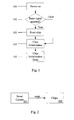
- Fig. 1 illustrates the behavior of the chip after power-on.
- step 101 the chip detects the reset signal, step 102. If the reset signal is keeping on, the chip will always be in a reset state, step 103. After the reset signal is off, the chip will start chip initialization, step 104, and get into service when initialization is done, in step 105.
- the power-on reset event should occur only once after power-on.
- Fig. 2 illustrates a traditional wire connection between a reset circuit 201 and chips 202.
- the reset circuit 201 After the power is on, the reset circuit 201 will detect the condition, and generate a reset cycle to all chips 202.
- the quality of a reset signal is very important.
- the reset signal has to be most nearly a square wave. Any instability may cause the system to become locked up. Such instabilities, such as a glitch, will improperly reset the chip.
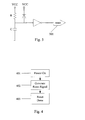
- Fig. 3 illustrates a simple power-on reset circuit. It is an analog circuit and relies on a capacitor C to detect the power-on condition. After the power is on, the capacitor C is not charged, and its voltage is zero. The power VCC will charge the capacitor C through resistor R. Before the capacitor C is fully charged, the circuit has enough time to reset other components 301. A length of the reset time is based on a value of resistor R and capacitor C, i.e. the RC pair. And after capacitor C is fully charged, the reset cycle is also finish. This makes sure the power-on reset event only occur once.
- the circuit or similar ones are widely used to perform the power-on function, and such a circuit is not costly. Since the output of RC pair is not a perfect square wave, a filter, like a Schmitt trigger, is also integrated into the circuit.
- step 401 the power-on event occurs and a reset signal is generated, in step 402. Thereafter, the reset is complete, in step 403, and the process ends.
- Fig. 1 illustrates a process of resetting and initializing a chip
- Fig. 2 illustrates a connection between a reset circuit and chips that receive a reset signal
- Fig. 3 illustrates a schematic of a power-on reset circuit
- Fig. 4 illustrates a process of powering on and generating the reset signal
- Fig. 5 illustrates a reset circuit within a chip, according to one embodiment of the present invention
- Fig. 6 illustrates a process of performing a power-on reset, according to one embodiment of the present invention.
- Fig. 7 illustrates a process of performing a power-on reset, according to an alternate embodiment of the present invention.
- the present invention proposes an alternative solution to the prior art external power-on reset circuits.
- a digital circuit namely a digital power on reset controller 501
- the reset circuit 501 can be built in a digital chip 502 easily. It can detect if the chip has been reset or not after power-on. If the chip 502 has not been reset after power on, the reset circuit 501 then generates the reset signal internally to reset the chip 502. Only digital components are used to construct the reset circuit 501. Since only digital components are required, the reset circuit 501 can be integrated into digital chips, and, thus, no external reset pin is need in this embodiment.
- the approach uses a set of registers called reset registers.
- the reset registers do not have any reset input. After power is on, the value of reset registers is supposed to be unknown.
- the value of the reset registers may be 0, 1, 2, or any random number. If the value of reset registers is compared to a magic number, like 0x55, 0xAA or any unique number, the result should be not equal.
- the reset circuit 501 Since the comparison of the reset register with the magic number is not equal right after power on, the reset circuit 501 will begin to initialize the reset registers with the unique magic number, thereby avoiding the reset circuit 501 from detecting the power-on event again. Then, the circuit generates the reset signal. Using a counter, the length of reset time is easily controlled. Since logic gates and registers can implement the approach, the generated reset signal is pure digital. It is easy to guarantee the quality of the signal.
- step 601 the power-on event commences.
- step 602 the values of the reset registers are compared with a magic number. If the magic number and the register values are the same, then the process ends, since there is no need for the reset signal to be generated.
- the reset registers are initialized, step 603, and the reset signal is generated, in step 604. Thereafter, the reset process is finished, in step 605.
- the value of the reset registers is equal to the magic number now. Thus, the reset signal generation event need not happen again. Only one reset event happens after power-on.
- the present invention has a set of reset registers and a magic number. If the reset registers are composed of n registers, then after power-on, the probability of the reset registers value come out to be the magic number is 1/(2 n ). The greater the number of reset registers, the lower the probability that a false match could occur and result in an increased correctness of the approach.
- the choice of magic number is also important. If all zeros or all ones were chosen as the magic number, then the reset registers with same physical characteristic may come out the value of all zeros or all ones. If the value with zeros and ones mixed is selected, the likelihood of false positive is reduced.
- the safest number is half of the bits being all zeros, and the other half is all ones, like 0x55 or 0xAA. It is rare for the reset registers to come out to such values after power-on.
- bias the storage device with a particular value to ensure that it will not coincidentally match the magic number.
- There are several methodologies that can be used to bias the storage device for the Reset Register during the power-on period i.e. bias the Reset Register as 0xAA if the specified magic number is 0x55, for example.
- Another method can be used when the Reset Register is made of flip-flops or latches cell with a low-active pre-set or pre-reset pins.
- the pre-set/pre-reset Reset Register is set to 0xAA during the power-on period. In the chip, 2ns is enough to do the pre-set or pre-reset for a flip-flop or latch cell. Additionally, the 100k-ohm resistor and 0.5p-farad capacitor are very tiny.
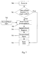
- step 703 is added, to filter the reset and do a synchronization to perform the desired function.
- the process flow is the same and the power-on reset task is processed as usual. However, in step 703, it is determined whether a signal from an external reset input, 702, to decide whether to manually reset the system or not.
- the power-on reset circuit During power-on, no matter whether the input from the external reset input 702 is zero or one, the power-on reset circuit will perform its function. After reset, once the external reset input is asserted, the reset circuit will be activated again.
- the reset filter and synchronization step 703 also performs a reset filtering function to filter the glitch input from external reset input 702, and synchronize the phase to system clock domain. This is important to avoid the issues associated with the analog systems discussed above.
- the digital power-on reset controller of the present invention provides a low cost way of generating the power-on reset signal. It is easy to implement and can be an embedded circuit for most chips that need the function. In addition, the input reset pin can be removed when there is no need for an external reset. Moreover, the signal quality of the rest signal is fully digital and less prone to glitches.
- the above-discussed configuration of the invention is, in a preferred embodiment, embodied on a semiconductor substrate, such as silicon, with appropriate semiconductor manufacturing techniques and based upon a circuit layout which would, based upon the embodiments discussed above, be apparent to those skilled in the art.
- a person of skill in the art with respect to semiconductor design and manufacturing would be able to implement the various modules, interfaces, and tables, buffers, etc. of the present invention onto a single semiconductor substrate, based upon the architectural description discussed above. It would also be within the scope of the invention to implement the disclosed elements of the invention in discrete electronic components, thereby taking advantage of the functional aspects of the invention without maximizing the advantages through the use of a single semiconductor substrate.
- the devices discussed herein may be any electronic device that utilizes a power-on reset. These devices may also include network devices and can include switches, routers, bridges, gateways or servers. These devices may also include power management devices that utilize a power-on reset.
Landscapes
- Electronic Switches (AREA)
Applications Claiming Priority (1)
| Application Number | Priority Date | Filing Date | Title |
|---|---|---|---|
| US11/132,280 US8395426B2 (en) | 2005-05-19 | 2005-05-19 | Digital power-on reset controller |
Publications (2)
| Publication Number | Publication Date |
|---|---|
| EP1724924A1 true EP1724924A1 (de) | 2006-11-22 |
| EP1724924B1 EP1724924B1 (de) | 2016-03-16 |
Family
ID=36940650
Family Applications (1)
| Application Number | Title | Priority Date | Filing Date |
|---|---|---|---|
| EP05026382.1A Expired - Lifetime EP1724924B1 (de) | 2005-05-19 | 2005-12-02 | Digitale Betriebs-Resetsteuerung |
Country Status (4)
| Country | Link |
|---|---|
| US (2) | US8395426B2 (de) |
| EP (1) | EP1724924B1 (de) |
| CN (1) | CN1866160B (de) |
| TW (1) | TWI425769B (de) |
Cited By (1)
| Publication number | Priority date | Publication date | Assignee | Title |
|---|---|---|---|---|
| GB2455567A (en) * | 2007-12-14 | 2009-06-17 | Icera Inc | A circuit for securing against non-reset of a device in power-up reset procedures |
Families Citing this family (8)
| Publication number | Priority date | Publication date | Assignee | Title |
|---|---|---|---|---|
| US7348815B2 (en) * | 2006-05-01 | 2008-03-25 | Taiwan Semiconductor Manufacturing Co., Ltd. | All-digital power-on reset device |
| US8493109B2 (en) * | 2010-03-31 | 2013-07-23 | Qualcomm Incorporated | System and method to control a power on reset signal |
| CN106324483B (zh) * | 2016-08-30 | 2019-07-30 | 歌尔科技有限公司 | 一种复位电路检测系统和检测方法 |
| CN108256356B (zh) * | 2016-12-29 | 2021-05-25 | 北京中电华大电子设计有限责任公司 | 一种抵抗芯片寄存器故障注入的方法 |
| CN108256319B (zh) * | 2016-12-29 | 2024-02-06 | 北京中电华大电子设计有限责任公司 | 一种延时锁止芯片的方法 |
| JP7135497B2 (ja) * | 2018-06-27 | 2022-09-13 | サンケン電気株式会社 | データ処理装置 |
| US10671763B2 (en) | 2018-11-01 | 2020-06-02 | Nvidia Corporation | Protecting circuits from hacking using a digital reset detector |
| CN116825006A (zh) * | 2023-06-25 | 2023-09-29 | 深圳同兴达科技股份有限公司 | 一种检测lcm模组复位管脚是否正常的方法 |
Citations (2)
| Publication number | Priority date | Publication date | Assignee | Title |
|---|---|---|---|---|
| US6278302B1 (en) * | 1999-06-03 | 2001-08-21 | Agere Systems Guardian Corp. | Digital power-up reset circuit |
| DE10204081A1 (de) * | 2002-02-01 | 2003-08-14 | Siemens Ag | Digitales Resetfilter für asynchrone Logikbausteine |
Family Cites Families (14)
| Publication number | Priority date | Publication date | Assignee | Title |
|---|---|---|---|---|
| US5377248A (en) * | 1988-11-29 | 1994-12-27 | Brooks; David R. | Successive-approximation register |
| US5376834A (en) * | 1993-03-05 | 1994-12-27 | Sgs-Thomson Microelectronics, Inc. | Initialization circuit for automatically establishing an output to zero or desired reference potential |
| JPH0850465A (ja) * | 1994-05-30 | 1996-02-20 | Sanyo Electric Co Ltd | シフトレジスタ及び表示装置の駆動回路 |
| US5553070A (en) * | 1994-09-13 | 1996-09-03 | Riley; Robert E. | Data link module for time division multiplexing control systems |
| US5559458A (en) * | 1995-05-11 | 1996-09-24 | Lucent Technologies Inc. | Reset circuit for a pipelined signal processor |
| US6854067B1 (en) * | 2000-10-30 | 2005-02-08 | Cypress Semiconductor Corporation | Method and system for interaction between a processor and a power on reset circuit to dynamically control power states in a microcontroller |
| US7243117B2 (en) * | 2001-02-07 | 2007-07-10 | Fdk Corporation | Random number generator and probability generator |
| JP3904859B2 (ja) * | 2001-07-30 | 2007-04-11 | シャープ株式会社 | パワーオンリセット回路およびこれを備えたicカード |
| TW587366B (en) * | 2003-03-25 | 2004-05-11 | Realtek Semiconductor Corp | Internal power-on reset circuit and method for low-voltage chip |
| JP4044020B2 (ja) * | 2003-06-10 | 2008-02-06 | シャープ株式会社 | 双方向シフトレジスタ、および、それを備えた表示装置 |
| US6956414B2 (en) * | 2004-02-17 | 2005-10-18 | Broadcom Corporation | System and method for creating a limited duration clock divider reset |
| US7242218B2 (en) * | 2004-12-02 | 2007-07-10 | Altera Corporation | Techniques for combining volatile and non-volatile programmable logic on an integrated circuit |
| US20060153453A1 (en) * | 2005-01-11 | 2006-07-13 | Thurgood Robin G | System and method for article detection |
| US7403051B1 (en) * | 2006-01-26 | 2008-07-22 | Xilinx, Inc. | Determining voltage level validity for a power-on reset condition |
-
2005
- 2005-05-19 US US11/132,280 patent/US8395426B2/en active Active
- 2005-12-02 EP EP05026382.1A patent/EP1724924B1/de not_active Expired - Lifetime
-
2006
- 2006-05-08 CN CN200610081913.6A patent/CN1866160B/zh not_active Expired - Fee Related
- 2006-05-19 TW TW095117862A patent/TWI425769B/zh not_active IP Right Cessation
-
2013
- 2013-02-06 US US13/760,888 patent/US8618849B2/en not_active Expired - Fee Related
Patent Citations (2)
| Publication number | Priority date | Publication date | Assignee | Title |
|---|---|---|---|---|
| US6278302B1 (en) * | 1999-06-03 | 2001-08-21 | Agere Systems Guardian Corp. | Digital power-up reset circuit |
| DE10204081A1 (de) * | 2002-02-01 | 2003-08-14 | Siemens Ag | Digitales Resetfilter für asynchrone Logikbausteine |
Cited By (3)
| Publication number | Priority date | Publication date | Assignee | Title |
|---|---|---|---|---|
| GB2455567A (en) * | 2007-12-14 | 2009-06-17 | Icera Inc | A circuit for securing against non-reset of a device in power-up reset procedures |
| US8196215B2 (en) | 2007-12-14 | 2012-06-05 | Icera Inc. | Security circuit for power up |
| GB2455567B (en) * | 2007-12-14 | 2012-12-26 | Icera Inc | Security circuit for power up |
Also Published As
| Publication number | Publication date |
|---|---|
| CN1866160A (zh) | 2006-11-22 |
| US20130207697A1 (en) | 2013-08-15 |
| CN1866160B (zh) | 2010-08-11 |
| US20060261868A1 (en) | 2006-11-23 |
| EP1724924B1 (de) | 2016-03-16 |
| US8395426B2 (en) | 2013-03-12 |
| US8618849B2 (en) | 2013-12-31 |
| TW200713814A (en) | 2007-04-01 |
| TWI425769B (zh) | 2014-02-01 |
Similar Documents
| Publication | Publication Date | Title |
|---|---|---|
| US8618849B2 (en) | Digital power on reset controller | |
| US7057427B2 (en) | Power on reset circuit | |
| US4929850A (en) | Metastable resistant flip-flop | |
| US8018256B2 (en) | Method and system for providing a power-on reset pulse | |
| US20040019718A1 (en) | Method for receiving user defined frame information structure (FIS) types in a serial-ATA (SATA) system | |
| US7746131B2 (en) | Reset signal filter | |
| US9685953B1 (en) | Low latency asynchronous interface circuits | |
| US7174473B2 (en) | Start detection circuit, stop detection circuit and circuit for the detection of data transmitted according to the IIC protocol | |
| KR930005838B1 (ko) | 디지탈 신호처리회로와 아나로그 신호처리 회로를 갖는 원칩 반도체 집적회로장치 | |
| JP4007027B2 (ja) | パワーオンリセット回路 | |
| TW293982B (de) | ||
| JPH0863264A (ja) | パワーオンリセット回路 | |
| US6924682B1 (en) | Latch circuit with metastability trap and method therefor | |
| JP2008502232A (ja) | 三値デコーダ回路および方法 | |
| CN114691221B (zh) | 控制电路及操作系统 | |
| US6781429B1 (en) | Latch circuit with metastability trap and method therefor | |
| US6378091B1 (en) | Test mode circuit capable of surely resetting test mode signals | |
| US10972092B2 (en) | Power-on reset circuit | |
| JP3690915B2 (ja) | 乱数発生回路を有する半導体装置 | |
| US20200341058A1 (en) | Time-limited debug mode | |
| US12231116B1 (en) | Digital power on reset circuit and method | |
| JPH05235705A (ja) | Rsフリップフロップ回路 | |
| CN114448203B (zh) | 控制电路以及对应方法 | |
| JPH08171435A (ja) | シリアルデータバス端末装置の電源オン/オフ時のノイズ低減回路 | |
| JPH11214973A (ja) | リセット回路 |
Legal Events
| Date | Code | Title | Description |
|---|---|---|---|
| PUAI | Public reference made under article 153(3) epc to a published international application that has entered the european phase |
Free format text: ORIGINAL CODE: 0009012 |
|
| AK | Designated contracting states |
Kind code of ref document: A1 Designated state(s): AT BE BG CH CY CZ DE DK EE ES FI FR GB GR HU IE IS IT LI LT LU LV MC NL PL PT RO SE SI SK TR |
|
| AX | Request for extension of the european patent |
Extension state: AL BA HR MK YU |
|
| RAP1 | Party data changed (applicant data changed or rights of an application transferred) |
Owner name: BROADCOM CORPORATION |
|
| 17P | Request for examination filed |
Effective date: 20070522 |
|
| 17Q | First examination report despatched |
Effective date: 20070625 |
|
| AKX | Designation fees paid |
Designated state(s): DE FR GB |
|
| GRAP | Despatch of communication of intention to grant a patent |
Free format text: ORIGINAL CODE: EPIDOSNIGR1 |
|
| INTG | Intention to grant announced |
Effective date: 20151002 |
|
| GRAS | Grant fee paid |
Free format text: ORIGINAL CODE: EPIDOSNIGR3 |
|
| GRAA | (expected) grant |
Free format text: ORIGINAL CODE: 0009210 |
|
| AK | Designated contracting states |
Kind code of ref document: B1 Designated state(s): DE FR GB |
|
| REG | Reference to a national code |
Ref country code: GB Ref legal event code: FG4D Ref country code: DE Ref legal event code: R081 Ref document number: 602005048652 Country of ref document: DE Owner name: AVAGO TECHNOLOGIES GENERAL IP (SINGAPORE) PTE., SG Free format text: FORMER OWNER: BROADCOM CORP., IRVINE, CALIF., US Ref country code: DE Ref legal event code: R081 Ref document number: 602005048652 Country of ref document: DE Owner name: AVAGO TECHNOLOGIES INTERNATIONAL SALES PTE. LT, SG Free format text: FORMER OWNER: BROADCOM CORP., IRVINE, CALIF., US |
|
| REG | Reference to a national code |
Ref country code: DE Ref legal event code: R096 Ref document number: 602005048652 Country of ref document: DE |
|
| REG | Reference to a national code |
Ref country code: DE Ref legal event code: R097 Ref document number: 602005048652 Country of ref document: DE |
|
| PLBE | No opposition filed within time limit |
Free format text: ORIGINAL CODE: 0009261 |
|
| STAA | Information on the status of an ep patent application or granted ep patent |
Free format text: STATUS: NO OPPOSITION FILED WITHIN TIME LIMIT |
|
| 26N | No opposition filed |
Effective date: 20161219 |
|
| REG | Reference to a national code |
Ref country code: DE Ref legal event code: R082 Ref document number: 602005048652 Country of ref document: DE Representative=s name: BOSCH JEHLE PATENTANWALTSGESELLSCHAFT MBH, DE Ref country code: DE Ref legal event code: R081 Ref document number: 602005048652 Country of ref document: DE Owner name: AVAGO TECHNOLOGIES GENERAL IP (SINGAPORE) PTE., SG Free format text: FORMER OWNER: BROADCOM CORPORATION, IRVINE, CALIF., US Ref country code: DE Ref legal event code: R081 Ref document number: 602005048652 Country of ref document: DE Owner name: AVAGO TECHNOLOGIES INTERNATIONAL SALES PTE. LT, SG Free format text: FORMER OWNER: BROADCOM CORPORATION, IRVINE, CALIF., US |
|
| GBPC | Gb: european patent ceased through non-payment of renewal fee |
Effective date: 20161202 |
|
| REG | Reference to a national code |
Ref country code: FR Ref legal event code: ST Effective date: 20170831 |
|
| PG25 | Lapsed in a contracting state [announced via postgrant information from national office to epo] |
Ref country code: FR Free format text: LAPSE BECAUSE OF NON-PAYMENT OF DUE FEES Effective date: 20170102 |
|
| PG25 | Lapsed in a contracting state [announced via postgrant information from national office to epo] |
Ref country code: GB Free format text: LAPSE BECAUSE OF NON-PAYMENT OF DUE FEES Effective date: 20161202 |
|
| REG | Reference to a national code |
Ref country code: DE Ref legal event code: R082 Ref document number: 602005048652 Country of ref document: DE Representative=s name: BOSCH JEHLE PATENTANWALTSGESELLSCHAFT MBH, DE Ref country code: DE Ref legal event code: R081 Ref document number: 602005048652 Country of ref document: DE Owner name: AVAGO TECHNOLOGIES INTERNATIONAL SALES PTE. LT, SG Free format text: FORMER OWNER: AVAGO TECHNOLOGIES GENERAL IP (SINGAPORE) PTE. LTD., SINGAPORE, SG |
|
| PGFP | Annual fee paid to national office [announced via postgrant information from national office to epo] |
Ref country code: DE Payment date: 20241210 Year of fee payment: 20 |
|
| REG | Reference to a national code |
Ref country code: DE Ref legal event code: R071 Ref document number: 602005048652 Country of ref document: DE |