EP1717855A1 - Compositions de pâtes conductrices à couche épaisse et leur utilisation dans des céramiques cocuité basse temperature (LTCC) et dispositifs - Google Patents
Compositions de pâtes conductrices à couche épaisse et leur utilisation dans des céramiques cocuité basse temperature (LTCC) et dispositifs Download PDFInfo
- Publication number
- EP1717855A1 EP1717855A1 EP06007769A EP06007769A EP1717855A1 EP 1717855 A1 EP1717855 A1 EP 1717855A1 EP 06007769 A EP06007769 A EP 06007769A EP 06007769 A EP06007769 A EP 06007769A EP 1717855 A1 EP1717855 A1 EP 1717855A1
- Authority
- EP
- European Patent Office
- Prior art keywords
- composition
- thick film
- layers
- green tape
- conductor
- Prior art date
- Legal status (The legal status is an assumption and is not a legal conclusion. Google has not performed a legal analysis and makes no representation as to the accuracy of the status listed.)
- Granted
Links
Images

Classifications
-
- H—ELECTRICITY
- H05—ELECTRIC TECHNIQUES NOT OTHERWISE PROVIDED FOR
- H05K—PRINTED CIRCUITS; CASINGS OR CONSTRUCTIONAL DETAILS OF ELECTRIC APPARATUS; MANUFACTURE OF ASSEMBLAGES OF ELECTRICAL COMPONENTS
- H05K1/00—Printed circuits
- H05K1/02—Details
- H05K1/09—Use of materials for the conductive, e.g. metallic pattern
- H05K1/092—Dispersed materials, e.g. conductive pastes or inks
- H05K1/097—Inks comprising nanoparticles and specially adapted for being sintered at low temperature
-
- H—ELECTRICITY
- H01—ELECTRIC ELEMENTS
- H01B—CABLES; CONDUCTORS; INSULATORS; SELECTION OF MATERIALS FOR THEIR CONDUCTIVE, INSULATING OR DIELECTRIC PROPERTIES
- H01B1/00—Conductors or conductive bodies characterised by the conductive materials; Selection of materials as conductors
- H01B1/20—Conductive material dispersed in non-conductive organic material
- H01B1/22—Conductive material dispersed in non-conductive organic material the conductive material comprising metals or alloys
-
- C—CHEMISTRY; METALLURGY
- C03—GLASS; MINERAL OR SLAG WOOL
- C03C—CHEMICAL COMPOSITION OF GLASSES, GLAZES OR VITREOUS ENAMELS; SURFACE TREATMENT OF GLASS; SURFACE TREATMENT OF FIBRES OR FILAMENTS MADE FROM GLASS, MINERALS OR SLAGS; JOINING GLASS TO GLASS OR OTHER MATERIALS
- C03C3/00—Glass compositions
- C03C3/04—Glass compositions containing silica
- C03C3/062—Glass compositions containing silica with less than 40% silica by weight
- C03C3/07—Glass compositions containing silica with less than 40% silica by weight containing lead
- C03C3/072—Glass compositions containing silica with less than 40% silica by weight containing lead containing boron
- C03C3/074—Glass compositions containing silica with less than 40% silica by weight containing lead containing boron containing zinc
-
- C—CHEMISTRY; METALLURGY
- C03—GLASS; MINERAL OR SLAG WOOL
- C03C—CHEMICAL COMPOSITION OF GLASSES, GLAZES OR VITREOUS ENAMELS; SURFACE TREATMENT OF GLASS; SURFACE TREATMENT OF FIBRES OR FILAMENTS MADE FROM GLASS, MINERALS OR SLAGS; JOINING GLASS TO GLASS OR OTHER MATERIALS
- C03C3/00—Glass compositions
- C03C3/04—Glass compositions containing silica
- C03C3/076—Glass compositions containing silica with 40% to 90% silica, by weight
- C03C3/089—Glass compositions containing silica with 40% to 90% silica, by weight containing boron
- C03C3/091—Glass compositions containing silica with 40% to 90% silica, by weight containing boron containing aluminium
-
- C—CHEMISTRY; METALLURGY
- C03—GLASS; MINERAL OR SLAG WOOL
- C03C—CHEMICAL COMPOSITION OF GLASSES, GLAZES OR VITREOUS ENAMELS; SURFACE TREATMENT OF GLASS; SURFACE TREATMENT OF FIBRES OR FILAMENTS MADE FROM GLASS, MINERALS OR SLAGS; JOINING GLASS TO GLASS OR OTHER MATERIALS
- C03C3/00—Glass compositions
- C03C3/04—Glass compositions containing silica
- C03C3/076—Glass compositions containing silica with 40% to 90% silica, by weight
- C03C3/102—Glass compositions containing silica with 40% to 90% silica, by weight containing lead
- C03C3/108—Glass compositions containing silica with 40% to 90% silica, by weight containing lead containing boron
-
- C—CHEMISTRY; METALLURGY
- C03—GLASS; MINERAL OR SLAG WOOL
- C03C—CHEMICAL COMPOSITION OF GLASSES, GLAZES OR VITREOUS ENAMELS; SURFACE TREATMENT OF GLASS; SURFACE TREATMENT OF FIBRES OR FILAMENTS MADE FROM GLASS, MINERALS OR SLAGS; JOINING GLASS TO GLASS OR OTHER MATERIALS
- C03C8/00—Enamels; Glazes; Fusion seal compositions being frit compositions having non-frit additions
- C03C8/02—Frit compositions, i.e. in a powdered or comminuted form
- C03C8/04—Frit compositions, i.e. in a powdered or comminuted form containing zinc
-
- C—CHEMISTRY; METALLURGY
- C03—GLASS; MINERAL OR SLAG WOOL
- C03C—CHEMICAL COMPOSITION OF GLASSES, GLAZES OR VITREOUS ENAMELS; SURFACE TREATMENT OF GLASS; SURFACE TREATMENT OF FIBRES OR FILAMENTS MADE FROM GLASS, MINERALS OR SLAGS; JOINING GLASS TO GLASS OR OTHER MATERIALS
- C03C8/00—Enamels; Glazes; Fusion seal compositions being frit compositions having non-frit additions
- C03C8/02—Frit compositions, i.e. in a powdered or comminuted form
- C03C8/10—Frit compositions, i.e. in a powdered or comminuted form containing lead
-
- C—CHEMISTRY; METALLURGY
- C03—GLASS; MINERAL OR SLAG WOOL
- C03C—CHEMICAL COMPOSITION OF GLASSES, GLAZES OR VITREOUS ENAMELS; SURFACE TREATMENT OF GLASS; SURFACE TREATMENT OF FIBRES OR FILAMENTS MADE FROM GLASS, MINERALS OR SLAGS; JOINING GLASS TO GLASS OR OTHER MATERIALS
- C03C8/00—Enamels; Glazes; Fusion seal compositions being frit compositions having non-frit additions
- C03C8/14—Glass frit mixtures having non-frit additions, e.g. opacifiers, colorants, mill-additions
- C03C8/18—Glass frit mixtures having non-frit additions, e.g. opacifiers, colorants, mill-additions containing free metals
-
- H—ELECTRICITY
- H01—ELECTRIC ELEMENTS
- H01L—SEMICONDUCTOR DEVICES NOT COVERED BY CLASS H10
- H01L23/00—Details of semiconductor or other solid state devices
- H01L23/48—Arrangements for conducting electric current to or from the solid state body in operation, e.g. leads, terminal arrangements ; Selection of materials therefor
- H01L23/488—Arrangements for conducting electric current to or from the solid state body in operation, e.g. leads, terminal arrangements ; Selection of materials therefor consisting of soldered or bonded constructions
- H01L23/498—Leads, i.e. metallisations or lead-frames on insulating substrates, e.g. chip carriers
- H01L23/49866—Leads, i.e. metallisations or lead-frames on insulating substrates, e.g. chip carriers characterised by the materials
- H01L23/49883—Leads, i.e. metallisations or lead-frames on insulating substrates, e.g. chip carriers characterised by the materials the conductive materials containing organic materials or pastes, e.g. for thick films
-
- H—ELECTRICITY
- H05—ELECTRIC TECHNIQUES NOT OTHERWISE PROVIDED FOR
- H05K—PRINTED CIRCUITS; CASINGS OR CONSTRUCTIONAL DETAILS OF ELECTRIC APPARATUS; MANUFACTURE OF ASSEMBLAGES OF ELECTRICAL COMPONENTS
- H05K3/00—Apparatus or processes for manufacturing printed circuits
- H05K3/46—Manufacturing multilayer circuits
-
- H—ELECTRICITY
- H01—ELECTRIC ELEMENTS
- H01L—SEMICONDUCTOR DEVICES NOT COVERED BY CLASS H10
- H01L2924/00—Indexing scheme for arrangements or methods for connecting or disconnecting semiconductor or solid-state bodies as covered by H01L24/00
- H01L2924/0001—Technical content checked by a classifier
- H01L2924/0002—Not covered by any one of groups H01L24/00, H01L24/00 and H01L2224/00
-
- H—ELECTRICITY
- H01—ELECTRIC ELEMENTS
- H01L—SEMICONDUCTOR DEVICES NOT COVERED BY CLASS H10
- H01L2924/00—Indexing scheme for arrangements or methods for connecting or disconnecting semiconductor or solid-state bodies as covered by H01L24/00
- H01L2924/095—Indexing scheme for arrangements or methods for connecting or disconnecting semiconductor or solid-state bodies as covered by H01L24/00 with a principal constituent of the material being a combination of two or more materials provided in the groups H01L2924/013 - H01L2924/0715
- H01L2924/097—Glass-ceramics, e.g. devitrified glass
- H01L2924/09701—Low temperature co-fired ceramic [LTCC]
-
- H—ELECTRICITY
- H05—ELECTRIC TECHNIQUES NOT OTHERWISE PROVIDED FOR
- H05K—PRINTED CIRCUITS; CASINGS OR CONSTRUCTIONAL DETAILS OF ELECTRIC APPARATUS; MANUFACTURE OF ASSEMBLAGES OF ELECTRICAL COMPONENTS
- H05K2203/00—Indexing scheme relating to apparatus or processes for manufacturing printed circuits covered by H05K3/00
- H05K2203/11—Treatments characterised by their effect, e.g. heating, cooling, roughening
- H05K2203/1131—Sintering, i.e. fusing of metal particles to achieve or improve electrical conductivity
-
- H—ELECTRICITY
- H05—ELECTRIC TECHNIQUES NOT OTHERWISE PROVIDED FOR
- H05K—PRINTED CIRCUITS; CASINGS OR CONSTRUCTIONAL DETAILS OF ELECTRIC APPARATUS; MANUFACTURE OF ASSEMBLAGES OF ELECTRICAL COMPONENTS
- H05K3/00—Apparatus or processes for manufacturing printed circuits
- H05K3/40—Forming printed elements for providing electric connections to or between printed circuits
- H05K3/4038—Through-connections; Vertical interconnect access [VIA] connections
- H05K3/4053—Through-connections; Vertical interconnect access [VIA] connections by thick-film techniques
- H05K3/4061—Through-connections; Vertical interconnect access [VIA] connections by thick-film techniques for via connections in inorganic insulating substrates
-
- H—ELECTRICITY
- H05—ELECTRIC TECHNIQUES NOT OTHERWISE PROVIDED FOR
- H05K—PRINTED CIRCUITS; CASINGS OR CONSTRUCTIONAL DETAILS OF ELECTRIC APPARATUS; MANUFACTURE OF ASSEMBLAGES OF ELECTRICAL COMPONENTS
- H05K3/00—Apparatus or processes for manufacturing printed circuits
- H05K3/46—Manufacturing multilayer circuits
- H05K3/4611—Manufacturing multilayer circuits by laminating two or more circuit boards
- H05K3/4614—Manufacturing multilayer circuits by laminating two or more circuit boards the electrical connections between the circuit boards being made during lamination
-
- H—ELECTRICITY
- H05—ELECTRIC TECHNIQUES NOT OTHERWISE PROVIDED FOR
- H05K—PRINTED CIRCUITS; CASINGS OR CONSTRUCTIONAL DETAILS OF ELECTRIC APPARATUS; MANUFACTURE OF ASSEMBLAGES OF ELECTRICAL COMPONENTS
- H05K3/00—Apparatus or processes for manufacturing printed circuits
- H05K3/46—Manufacturing multilayer circuits
- H05K3/4611—Manufacturing multilayer circuits by laminating two or more circuit boards
- H05K3/4626—Manufacturing multilayer circuits by laminating two or more circuit boards characterised by the insulating layers or materials
- H05K3/4629—Manufacturing multilayer circuits by laminating two or more circuit boards characterised by the insulating layers or materials laminating inorganic sheets comprising printed circuits, e.g. green ceramic sheets
Definitions
- the invention relates to thick film conductor compositions, including via-fill conductor compositions, which are useful in the manufacture of Low Temperature Co-fireable Ceramic (LTCC) multilayer ceramic circuits and devices, as well as the LTCC circuits and devices themselves.
- the invention further relates to the use of the thick film compositions, circuits and devices in microwave and other high frequency applications.
- LTCC Low Temperature Co-fireable Ceramic
- An interconnect circuit board of an LTCC design is a physical realization of electronic circuits or subsystems made from a number of extremely small circuit elements that are electrically and mechanically interconnected. It is frequently desirable to combine these diverse electronic components in an arrangement so that they can be physically isolated and mounted adjacent to one another in a single compact package and electrically connected to each other and/or to common connections extending from the package.
- LTCC complex electronic circuits generally require that the circuit be constructed of several layers of conductors separated by insulating dielectric layers.
- the conductive layers are interconnected between levels by electrically conductive pathways, called vias, through a dielectric layer.
- the conductors useful in LTCC technology are typically thick film conductors.
- LTCC multilayer structures allow a circuit to be more compact than traditional Al 2 O 3 substrates by allowing vertical integration.
- thick film conductors are comprised of an active (conductive) metal and inorganic binders, both of which are in finely divided form and are dispersed in an organic vehicle.
- the conductive phase is ordinarily gold, palladium, silver, platinum or alloy thereof, the choice of which depends upon the particular performance characteristics which are sought, e.g., resistivity, solderability, solder leach resistance, bondability, adhesion, migration resistance and the like.
- additional performance characteristics are sought for internal conductor lines and via conductors which include minimization of conductor line "sinking" into the top and bottom dielectric layers on firing, minimal resistivity variation on repeated firing, optimal interface connectivity of line conductor to that of via-fill conductor, and optimal interface bonding of via-fill conductor to that of surrounding ceramic materials.
- LTCC thick film compositions and tapes have been used in prior art high frequency applications, such as telecommunications, automotive or military applications including radar, for its multilayer, cofiring and flexible design capabilities.
- Many properties are required of the conductors used in the fabrication of multilayer circuits for high frequency including microwave applications, including desired resistivity, solderability, solder leach resistance, wire bondability, adhesion, migration resistance, and long term stability.
- U.S. Patent Number 5,744,232 to Bailey discloses a thick film metallization compatible with LTCC that display very low microwave insertion losses commensurate with those of thin film gold.
- the electrical performance of the metallization is attained by using a spherical metal particle shape and uniform particle size distribution in the thick film paste.
- the present invention overcomes problems associated with prior art thick film conductor compositions for use in LTCC and microwave applications.
- the present invention provides thick film compositions and LTCC structures, which provide superior refire stability.
- the present invention is directed to a thick film composition for use in low temperature co-fired ceramic circuits comprising, based on weight percent total thick film composition:
- the present invention is further directed to methods of forming multilayer circuits utilizing the above composition and the use of the composition in high frequency applications (including microwave applications).
- the invention is directed to a novel noble metallization for use in the manufacture of printed conductors for LTCC ceramics which have outstanding electrical properties on repeated firing of the devices, and other desired conductor properties in the application of both conventional and "green" electronic components and complex electronic devices.
- the invention is directed to a series of metal metallizations suitable for the manufacture of pure silver, gold and mixed metal electronic devices, which is admixture of: (a) 30-98% by weight finely divided conductive particles selected from noble metal, alloys of noble metals, and mixtures thereof, (b) 0.2-20% by weight finely divided particles selected from the group consisting of one or more refractory glasses wherein said refractory glasses have little/no miscibility to the remnant glasses present after the crystallization of the LTCC tape glasses, (d) 0.1-5% by weight inorganic metal oxides and /or inorganic compounds/or organometallics capable of controlling the densification, sintering and grain growth of the conductor composites.
- the invention is directed to screen-printable and/or stencil-applicable paste comprising the above-described metallization dispersed in organic medium.
- the invention is directed to conductive elements comprising a nonconductive LTCC ceramic substrate having a conductive pattern and connecting or non connecting via-fill conductive pattern affixed thereon, formed by printing a pattern of above-described screen-printable and/or stencil-applying paste and firing the printed and/or laminated LTCCs to effect volatization of the organic medium and liquid phase sintering of the inorganic materials and metallization.
- the invention is directed to a process for making conductors alone and/or in conjunction with via-fills comprising (a) applying patterned thick film of the above-described screen-printable paste to a non conductive ceramic substrate, (b) drying the film at a temperature below 200°C and (c) firing the dried film to effect liquid phase sintering of the inorganic materials and metallization.
- the main components of the thick film conductor composition(s) of the present invention are electrically conductive noble metal powders, alloys of noble metal powders and mixtures thereof; one or more inorganic binders selected from (a) refractory glass compositions with a specific viscosity (log n) in the range of 6-7.6 at the firing temperature of the LTCC circuit, (b) 0.1-5 weight percent of an additional inorganic binder selected from (1) metal oxides of Zn, Mg, Co, Al, Zr, Mn, Ni, Cu, Ta, W.
- inorganic binders selected from (a) refractory glass compositions with a specific viscosity (log n) in the range of 6-7.6 at the firing temperature of the LTCC circuit, (b) 0.1-5 weight percent of an additional inorganic binder selected from (1) metal oxides of Zn, Mg, Co, Al, Zr, Mn, Ni, Cu, Ta, W.
- La and other "glass network-modifying" refractory metal oxides (2) precursors of the metal oxides of (1); (3) non-oxide borides; (4) non-oxide silicides; and (5) mixtures thereof, and (c) mixtures thereof; dispersed in organic medium.
- the components are discussed herein below.
- the finely divided metals used in the invention can be of those selected from noble metal, alloys of noble metals, and mixtures thereof, many of which are commercially available.
- the particle size of the above-described metallic materials is not narrowly critical from the standpoint of their technical effectiveness in the invention. However, they should, of course, be of a size appropriate to the manner in which they are applied, which is usually screen-printing and/or stencil-applying, and to the firing conditions.
- particle size and morphology of the above-mentioned metal powders should be appropriate in screen-printing and /or stencil-applying over non-fired ceramic tape of thickness between 2 mil to 10 mil and to the laminating conditions of the composite and to the firing conditions.
- the metallic material should be no bigger than 10 um and preferably should be below about 5um.
- the available particle size of the metals is as low as 0.1-10 um for palladium, from 0.1 to 10um for silver, 0.2-10 um for platinum and from 0.5-10um for gold.
- the ratio of Pd/Ag metal powders can vary between 0.06 and 1.5 preferably between 0.06 and 0.5.
- the ratio of Pt/Ag metal powders can vary between 0.003 to 0.2 and preferably 0.003 to 0.05. Similar ratios can be used in the case of Pt/Pd/Au.
- the metal powders can have either flake or non-flake morphology.
- the non-flake powders can be irregularly shaped or spherical.
- flake morphology is meant a metal powder whose predominant shape is flake as determined by scanning electron microscopy.
- Such flake silvers have an average surface area of approximately 1 m2/g and solid contents of approximately 99-100% by weight.
- Non-flake silver powders typically have an average surface area to weight ratio of 0.1-2.0 m2/g and solid contents of approximately 99-100% by weight.
- Palladium metal powder has an average surface area to weight ratio of 2.0-15.0 m2/g, preferably, 7.0-11.0 m2/g and solid contents of approximately 99-100% by weight.
- Platinum metal powder has a surface area to weight ratio of approximately 10m2/g to 30 m2/g and a solids content of 98-100% by weight.
- gold powders used in embodiments of the present invention include gold metal powders which typically have a particle size distribution (PSD) d50 -0.5 to 5 um, measured using Scanning Electron Microscope (SEM) and a solids content of 99-100% by weight.
- PSD particle size distribution
- SEM Scanning Electron Microscope
- the gold metal powders are mono-sized, comprise few twins, and have a tight PSD.
- spherical metallic powders are utilized. These spherical metallic powders, when packed have a greater particle-to-particle contact versus flake and other shaped powders, which gives rise to a metal-to-metal contact and thus a relatively continuous flow of electrons for conduction when combined with the other components of the present invention.
- metal spherical particles allow for "tetrahedral" and/or “octrahedral” voids, wherein the specific inorganic binders of the present invention, such as metal oxides and/or glasses described below, may settle and upon processing the inorganic binders soften and hold the structure together in a uniform honeycomb-type structure with superior metal-to-metal contact and more continuous electron flow as compared to prior art compositions.
- spherical metallic particles with an average particle size distribution in the range of 1 to 4 microns are preferred.
- an average particle size of 2 to 3 microns is preferred.
- the inorganic binders of the present invention are one or more inorganic binders selected from (1) 0.2-20 weight percent of one or more refractory glass compositions with a specific viscosity (log n) in the range of 6-7.6 at the firing temperature of said circuit, (2) 0.1-5 weight percent of an additional inorganic binder selected from (i) metal oxides, (ii) precursors of metal oxides; (iii) non-oxide borides; (iv) non-oxide silicides; and (v) mixtures thereof, and (3) mixtures thereof.
- an additional inorganic binder selected from (i) metal oxides, (ii) precursors of metal oxides; (iii) non-oxide borides; (iv) non-oxide silicides; and (v) mixtures thereof, and (3) mixtures thereof.
- the glass component of the conductor compositions of this invention is a, high-softening point, high viscosity glass at 0.2-20 parts by weight level and, preferably, at 1-15 parts level.
- high-softening point glass is one having a softening point 600-950°C, preferably, 750-870°C as measured by the parallel plate viscosity measuring techniques (ASTM method).
- the glass utilized in this invention must also be immiscible or have only partial miscibility with the remnant glasses present in the LTCC substrate glasses at the firing conditions.
- Upon firing of an LTCC structure glasses present in the LTCC dielectric "green” tape will partially crystallize and result in the formation of very low melting "remnant glasses” along with the high melting inorganic crystalline materials.
- the chemistry of the "remant” glass will be different than that of the "parent” glass; as a result, the softening point and other properties of "remant” glass will also be different from its “parent” glass.
- the viscosity of the "remant” glass at the LTCC firing temperature will be lower than the "parent” glass.
- cofired conductors can react with these low melting "remnant glasses” resulting in undesirable results such as: (1) increased resistance of the conductors; (2) conductor lines which "sink” within the dielectric tape on refire; and (3) conductors which completely disperse within the dielectric upon multiple refires.
- these remnant glasses can migrate into the via fill conductor compositions of the prior art and crystallize or leave remnant glasses at the via cavity which results in a very high conductor resistance.
- a glass having a specific viscosity (log n) of ⁇ 6 to ⁇ 7.6 at the firing temperature which is capable of reduced intermixing with glasses present in the LTCC substrate glasses, but at the same time capable of aiding the sintering processes of the metallization is preferred.
- Typical examples of glasses meeting the above criteria are of the "alumino-boro-silicate glass network” type and may contain "glass network modifying" ions, selected from ions of Ca, Ba, Ti, Fe, Mg, Na, K, and mixtures thereof.
- Representative glasses include the following composition comprising, as described based on weight percent total glass composition, 40-60% SiO2, 10-20% Al2O3, 10-15% B2O3, 15-25% CaO, 1-5% selected from the other above-mentioned "network modifying" ions.
- a particularly preferred glass comprises, based on weight percent total glass composition, 55%SiO2, 14% Al2O3, 7.5% B203, 21.5% CaO, and the balance 2% the above-mentioned "networking modifying" ions.
- Another preferred glass comprises, based on weight percent total glass composition, 56.5% SiO2, 9.1 % Al203, 4.5% B2O3, 15.2% BaO, 10.0% CaO and the balance 5% selected from the other above-mentioned "network modifying" ions.
- the glasses are prepared by conventional glass-making techniques, by mixing the desired components in the desired proportions and heating the mixture to form a melt. As is well-known in the art, heating is conducted to a peak temperature and for a time such that the melt becomes entirely liquid and homogenous. In the present work the components are premixed in a polyethylene jar with plastic balls and melted in a platinum crucible at 1350-1400°C. The melt is heated at the peak temperature for 1-1.5 hours. The melt is then poured into cold water. The maximum temperature of the water during quenching is kept as low as possible by increasing the volume of water to melt ratio.
- the crude frit after separation from water, is freed from residual water by drying in air or displacement of water by rinsing with methanol, or other suitable method.
- the crude frit is the ball-milled for 6-7 hours in alumina containers using alumina balls. Alumina picked up by the materials, if any, is not within the observable limits as measured by X-ray diffraction analysis.
- the excess solvent is removed by decantation and the frit powder is hot air-dried.
- the dried powder is then screened through a 325 mesh screen to remove any large particles.
- the major two properties of the frits are: it aids the sintering of the inorganic crystalline particulate matters and minimizes the intermixing of conductor materials with remnant glasses present in the LTCC ceramics.
- the metal oxides and non-oxides, such as borides and silicides, which are suitable for the practice of the invention are those which are capable of reacting with remnant glasses of the tape and increase the viscosity of the remnant glasses when the composition of the invention is cofired with the tape, either on the surface or buried.
- the binders useful in the present invention should act as "sintering inhibitors" for the metal powders during firing of the system. Thus, minimizing the densification of the line conductors and via-fill conductors.
- Suitable inorganic oxides are those based on Zn2+, Mg2+, Co2+, Al3+ Zr4+, Mn2+, Ni2+, Cu2+, Ta3+, W4+, La3+ and other "glass network modifying" refractory oxides and complex oxides such as copper bismuth ruthenate, and organometallic compounds such as organotitanate those disclosed in U.K. Pat. No. 772,675 and U.S. Pat. No 4,381,945 , incorporated herein, that will decompose into finely divided powders of metal oxides during the firing of the system.
- the particle size of the metal oxides or precursors should be the size appropriate to the manner in which the composition of the invention is applied, which usually by screen printing, thus the particle size should be no larger than 15um and preferably should be below 5um.
- the inorganic components are typically dispersed into an organic medium by mechanical mixing to form viscous compositions called "pastes" having suitable consistency and rheology for printing.
- a wide variety of inert liquids can be used as organic medium.
- the rheological properties of the medium must be such that they lend good application properties to the composition, including: stable dispersion of solids, appropriate viscosity and thixotropy for screen printing, acceptable unfired "green” strength, appropriate wettability of the substrate and the paste solids, a good drying rate, and good firing and burn out properties.
- the organic medium is typically a solution of polymer(s) in solvent(s). Additionally, a small amount of additives, such as surfactants, may be a part of the organic medium.
- the most frequently used polymer for this purpose is ethyl cellulose.
- Other examples of polymers include ethylhydroxyethyl cellulose, wood rosin, mixtures of ethyl cellulose and phenolic resins, polymethacrylates of lower alcohols, and monobutyl ether of ethylene glycol monoacetate can also be used.
- the most widely used solvents found in thick film compositions are ester alcohols and terpenes such as alpha- or beta-terpineol or mixtures thereof with other solvents such as kerosene, dibutylphthalate, butyl carbitol, butyl carbitol acetate, hexylene glycol and high boiling alcohols and alcohol esters.
- volatile liquids for promoting rapid hardening after application on the substrate can be included in the vehicle.
- Various combinations of these and other solvents are formulated to obtain the viscosity and volatility requirements desired.
- the inorganic particles are mixed with an inert liquid medium (vehicle or medium) typically by mechanical mixing (e.g. on a roll mill) to form a paste-like composition having suitable consistency and rheology for screen printing and /or stencil applying.
- a paste-like composition having suitable consistency and rheology for screen printing and /or stencil applying.
- the latter is printed as a "thick film" on LTCC green tapes in the conventional manner.
- Any inert liquid may be used as the vehicle.
- Various organic liquids, with or without the thickening and/or stabilizing agents and/or other common additives may be used as the vehicle. The only specific criteria of the vehicle is that it must be chemically compatible to the organics present in the LTCC green tapes.
- organic liquids which can be used are the aliphatic alcohols, esters of such alcohols, for example, acetates and propionates, terpenes such as pine oil, terpinol and the like, texanol and the like, solutions of resins such as ethyl cellulose in solvents as pine oil, and the monobutyl ether of ethylene glycol monoacetate.
- the vehicle may contain volatile liquids to promote fast setting after application to the tape.
- the ratio of vehicle to solids in the dispersions can vary considerably and depends upon the manner in which the dispersion is to be applied and the kind of vehicle used and furthermore the use of the conductors are for the conductor lines and/or via-fill conductor connections. Normally to achieve good coverage the dispersions will comprise 60-98% solids and 40-2% organic medium (vehicle).
- the compositions of the present invention may, of course, be modified by the addition of other materials, which do not affect its beneficial characteristics. Such formulations are well within the skill of the art.
- the conductor composition(s) of the present invention may be used in conjunction with uncured ceramic material, such as Green TapeTM Low Temperature Cofired Ceramic (LTCC), and various other paste components, to form a multilayer electronic circuit.
- Green TapeTM is typically used as a dielectric or insulating material for multilayer electronic circuits.
- a sheet of Green TapeTM is blanked with registration holes in each corner to a size somewhat larger than the actual dimensions of the circuit.
- via holes are formed in the Green TapeTM . This is typically done by mechanical punching, however, any suitable method may be utilized. For example, a sharply focused laser can be used to volatilize and form via holes in the Green TapeTM .
- a thick film conductive composition forms the interconnections between layers.
- the thick film conductive composition disclosed herein may be utilized as a via-fill composition.
- This conductive via-fill composition is usually applied by standard screen printing techniques, however, any suitable application technique may be employed.
- Each layer of circuitry is typically completed by screen printing conductor tracks. These tracks can utilize compositions of the present invention, or other suitable conductor compositions, or a combination thereof.
- resistor inks or high dielectric constant inks can be printed on selected layer(s) to form resistive or capacitive circuit elements. Conductors, resistors, capacitors and any other components are typically formed by conventional screen printing techniques and are deemed as functional layers.
- the conductor composition(s) of the present invention may be printed on the outermost layers of the circuit, either before or after lamination. Additionally, the conductor composition(s) of the present invention may be used on one or more of the inner layers of the circuit, as well. Furthermore, embodiments of the conductor composition(s) of the present invention may be used as a via-fill composition, as well. It is understood by those skilled in the art that the circuit may comprise "blank layers" or layers of dielectric or insulating material on which no functional conductive, resistive, or capacitive layers are deposited.
- the outermost layers of the circuit are used to attach components.
- Components are typically wire-bonded, glued or soldered to the surface of fired parts.
- the individual layers are collated and laminated.
- a confined uniaxial or isostatic pressing die is typically used to ensure precise alignment between layers.
- the assemblies are trimmed to an appropriate size after lamination or after firing. Firing is typically carried out in a conveyor belt furnace or in a box furnace with a programmed heating cycle.
- the tape may be either constrained or free sintered during the firing process.
- the methods disclosed in U.S. 4,654,095 to Steinberg and U.S. 5,254,191 to Mikeska may be utilized, as well as others known to those skilled in the art.
- firing means heating the assembly in an oxidizing atmosphere, such as air to a temperature, and for a time sufficient to volatilize (burn-out) the organic material in the layers of the assemblage and allow reaction and sintering of the inorganic components of both the tape and conductors.
- "Firing” causes the inorganic components in the layers, to react or sinter, and thus density the entire assembly, thus forming a fired article.
- This fired article may be a multilayered circuit used in telecommunications, military or automotive applications (such as automotive position sensors, radar, transmit receive modules, antennas etc).
- a typical Green TapeTM layer may have contain one or more conductive traces, conductive vias, resistors and/or capacitors.
- microwave applications are defined herein as applications which require a frequency in the range of 300 MHz to 300 GHz (3x10 ⁇ 8 to 3x10 ⁇ 11 Hz).
- the present invention is useful in high frequency applications such as transmit/receive modules and radar applications.
- some of the embodiments of the present invention are useful in the formation of microwave circuit components including, but not limited to: antenna, filters, baluns, beam former, I/O's, couplers, feedthroughs (via or EM coupled), wirebond connection, and transmission lines.
- the thick film compositions of the present invention were prepared according to the following general methodology.
- the inorganic solids are mixed with the organic medium and dispersed with suitable equipment, such as a three-roll mill, to form a suspension, resulting in a composition for which the viscosity will be in the range of 100-200 Pascal-seconds at a shear rate of 4 sec-1 for the line conductor compositions and the corresponding value for via-fill conductors is 1000-5000 Pascal-seconds.
- the formulation was carried out in the following manner: The ingredients of the paste, minus about 2-5% of the organic components, were weighed together in a container. The components were then vigorously mixed to form a uniform blend; then the blend was passed through dispersing equipment, such as a three roll mill, to achieve a good dispersion of particles. A Hegman gauge was used to determine the state of dispersion of the particles in the paste. This instrument consists of a channel in a block of steel that is 25um deep (1 mil) on one end and rams up to 0" (i.e., 0-25 um range) depth at the other end. A blade was used to draw down paste along the length of the channel.
- the composition was then applied to a substrate, such as alumina or simliar refractory ceramics, in this particular case, to the "green tape".
- the "green tape” was formed by casting a 1-20 mil, preferably 2-10 mil, thin layer of a slurry dispersion of the glass and ceramic filler fine particulates, polymeric binder(s) and solvent(s) as described in the art of "tape casting” into a flexible substrate, and heating the cast layer to remove the volatile solvent.
- the tape is blanked into sheets or provided in roll form. This green tape is used as an insulating substrate for multilayer electronic circuits/devices, in place of conventional substrates, such as alumina and other refractory ceramic substrates.
- the green tape sheet is blanked with registration holes at the four corners, and via holes to connect the different layers of conductors using mechanical punching.
- the size of via holes varies depending on circuit design and property requirements.
- the interconnections of circuit between conductor track layers of the tape are typically applied by screen printing the conductive inks in the via holes.
- the conductive line compositions of the present invention were applied to a sheet of green tape, by the process of screen printing, to a wet thickness of about 10-30 um and the via holes were filled with respective conductive via compositions.
- each layer of tape is printed with conductor lines and via holes as appropriate to the circuit design, the individual layers are collated, laminated and pressed using uniaxial or isostatic pressing die and techniques as described elsewhere in the art of tape pressing/lamination techniques. It will be recognized by those skilled in the art that in each of the laminating steps the printed tape layers must be accurate in registration so that the vias are properly connected to the appropriate conductive lines of the adjacent functional layer, and in the case of thermal vias, each via will be connected appropriately to the next one.
- Firing to effect sintering of the green tape compositions and of the inorganic binder as well as the finely divided particles of metal is preferably done in a well ventilated belt conveyor furnace or programmed box furnace with a temperature profile that will allow de-polymerization of polymers; and/or burnout of the organic matter at about 300-600°C., a period of maximum temperature of about 800- 950°C., lasting about 5-20 minutes, followed by a controlled cool down cycle to prevent over-sintering and crystal growth, unwanted chemical reactions at intermediate temperatures, or substrate/fired ceramic tape fracture from too rapid cool down.
- the overall firing procedure will preferably extend over a period of between 3.5 to 5 hours, and in certain cases it could take up to 24 hours or more depending on the number of layers of green tapes laminated together and/or the thickness of the green tape layers.
- the fired thickness of the conductor can range from about 5 to about 15 um, depending on the percent of solids, the type of screen the composition is printed with, the printer set up, and degree of sintering of the inorganic solids.
- the thickness of via conductors vary depending on the thickness of the green tape used and degree of sintering of the via composition. In order to avoid two major defects, dimpling and posting of the vias, the selection of viscosity and solid content of the composition is important. In general, increased solid content could result in posting and lower solid content will result in dimpling.
- the conductor compositions of this invention can be printed as film onto the green tapes or ceramic substrates, or onto other thick films either by using an automated printer or a hand printer in the conventional manner.
- automation screen printing techniques are employed, using 200 to 325 mesh screen with 0.5 um emulsion thickness.
- Conventional stencil printing techniques are also can be used, particularly for filling the smaller vias of size 4-8 um.
- a "daisy chain” pattern shown in Figures (1, 3 and 4) of the conductor formulation to be tested was screen printed upon green sheets of tapes, laminated, and fired in a belt furnace using a "tape heating and cooling profile" as described earlier.
- the "daisy chain” pattern consisted of over 5000 squares of conductor lines and over 570 via-fill conductors connected in series. Any break in the line conductors and/or via-fill connections resulted in infinite resistance.
- the test parts were mounted on terminal posts and electrically connected to a digital ohm-meter. The temperature was adjusted to 25°C. The total resistance values in milli-ohms was divided by the total number of conductor squares, excluding the area of the via-fill conductors. The results were recorded as milli-ohms per square.
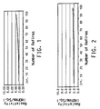
- Figure 2 represents a buried serpentine test of a silver metal system.
- the buried serpentine test pattern consisted of conductive lines of 6 mil in width with a length that gave approximately 5,000 squares printed on dielectric tape and laminated with at least one layer of dielectric tape.
- the structure was fired in a typical LTCC firing profile for approximately 3.5 hours, resistance was measured, and refire was performed at a 30 minute thick film profile. Resistance was measured after each firing.
- Typical dielectric "green" tapes useful in the present invention include those disclosed in U.S. Patent No. 6,147,019 . Additionally, DuPont Product Nos. 943 Green TapeTM and 944 Green TapeTM (available from E. I. du Pont de Nemours and Company) are further examples of those useful in the present invention.
- Glasses A, B, C, and D represent glasses that are useful in the present invention.
- Table 1 GLASS FRIT COMPOSITIONS Glass Composition (in weight percent total glass frit composition) A B C D Silicon Dioxide 30.0 55.0 33.1 56.5 Aluminum Trioxide 10.1 14.0 6.7 9.1 Boron Oxide 8.0 7.5 0.0 4.5 Barium Oxide 26.1 0.0 23.1 0.0 Calcium Oxide 6.0 21.5 4.5 8.6 Magnesium oxide 1.7 1.0 0.0 0.0 Strontium Oxide 0.0 0.0 13.5 0.0 Zirconium Oxide 0.0 0.0 3.5 0.0 Zinc Oxide 10.0 0.0 15.6 0.0 Lead oxide 0.0 0.0 0.0 17.2 Alkali oxides 0.0 0.5 0.0 4.1 Titanium Oxide/iron oxide 8.1 0.5 0.0 0.0
- Non-flake silver powders represented below have an average surface area to weight ratio of 0.1-2.0 m2/g.
- Palladium metal powders represented below have an average surface area to weight ratio of 2.0-15.0 m2/g.
- Platinum metal powders represented below have an average surface area to weight ratio of approximately 10m2/g to 30 m2/g.
- the average particle size distribution of the gold metal powders is in the range of 1-4 microns.
- Example 1 Gold via Fill Conductor -1
- Example 2 Gold via Fill Conductor -2
- Gold Powder 89.8 Aluminum Oxide 2.1
- Other Oxides 3.2 Ethyl cellulose/terpineol-based medium represents the balance Gold powder PSD d50 ⁇ 1-2um
- Example 3 Palladium-Silver Transition via Fill Conductor for mixed metal system
- Example 4 Palladium-Silver-Platinum Transition via Fill Conductor for mixed metal system
- Gold powder 80.7 Frit powder C 0.8 Ethyl cellulose/terpineol- based medium represents the balance Gold powder PSD d50 ⁇ 2-3 um
- Gold powder 78.0 Frit powder C 0.7 Ethyl cellulose/terpineol- based medium represents the balance Gold powder PSD ⁇ d50 4-5 um
- Gold powder 80.7 Frit powder D 0.8 Ethyl cellulose/terpineol- based medium represents the balance Gold powder PSA d50 ⁇ 2-3 um
- Silver Powder 90.9 Frit powder B 1.2 Ethyl cellulose/texanol- based medium represents the balance Silver powder SA 0.1 -1.5m2/gm
- Silver powder 89.5 Frit powder D 1.2 Ethyl cellulose/texanol-based medium represents the balance Silver powder SA ⁇ 0.1 - 1.5 m2/gm
- Example 10 Silver Ground Plane & Inner Conductor
- Organo metallics 1.0 Ethyl cellulose/texanol-based medium represents the balance Silver powder SA 0.1 ⁇ 1.5 m2/gm
- Example 11 Silver ⁇ Palladium Solderable Top Conductor
- Silver powder 53.5 Palladium powder 13.6 Copper bismuth ruthenate 5.1 Copper oxide 0.5 Ethylcellulose/terpineol-based medium represents the balance Flake Silver SA ⁇ 0.60-0.90 m2/gm Tap density 4.0-6.0 g/ml
- Standard commercially available LTCC thick film conductors Product Nos. 6142 and 6145 (available from E. I. du Pont de Nemours and Company) were printed over low loss LTCC green tapes and fired at standard LTCC firing profile. Analysis of the parts showed that most of the parts failed to get a resistivity reading. Scanning Electron Micrographs (SEM) of the failed parts were taken and noted partially “dissolved” conductor lines and growth of elongated crystals consisting of dielectric ingredients within the conductor lines. Some parts showed unacceptable levels of high resistivity. On refiring, the resistivity of these parts further increased.
- Standard LTCC conductor compositions contain glass binders that are miscible with the remnant glass present in the low-loss LTCC dielectric tape.
- dielectric components diffused into the conductor, resulting in increased the resistivity and/or crystals of tape ingredients grew within the conductors which causes the break in the conductor path and/or conductor lines are "sinking" in the low viscosity remnant glass present in the LTCC".
Applications Claiming Priority (2)
| Application Number | Priority Date | Filing Date | Title |
|---|---|---|---|
| US67443305P | 2005-04-25 | 2005-04-25 | |
| US11/398,337 US7611645B2 (en) | 2005-04-25 | 2006-04-05 | Thick film conductor compositions and the use thereof in LTCC circuits and devices |
Publications (2)
| Publication Number | Publication Date |
|---|---|
| EP1717855A1 true EP1717855A1 (fr) | 2006-11-02 |
| EP1717855B1 EP1717855B1 (fr) | 2015-07-01 |
Family
ID=36647809
Family Applications (1)
| Application Number | Title | Priority Date | Filing Date |
|---|---|---|---|
| EP06007769.0A Expired - Fee Related EP1717855B1 (fr) | 2005-04-25 | 2006-04-13 | Compositions de pâtes conductrices à couche épaisse et leur utilisation dans des céramiques cocuité basse temperature (LTCC) et dispositifs |
Country Status (6)
| Country | Link |
|---|---|
| US (1) | US7611645B2 (fr) |
| EP (1) | EP1717855B1 (fr) |
| JP (1) | JP4817951B2 (fr) |
| KR (2) | KR100796892B1 (fr) |
| CN (1) | CN1913044B (fr) |
| TW (1) | TWI348711B (fr) |
Cited By (5)
| Publication number | Priority date | Publication date | Assignee | Title |
|---|---|---|---|---|
| EP1788616A2 (fr) * | 2005-11-22 | 2007-05-23 | E.I. Dupont De Nemours And Company | Compositions de conducteur à couche épaisse et technique de traitement correspondante, pour une utilisation dans ces circuits et dispositifs électroniques multicouches |
| KR100796892B1 (ko) | 2005-04-25 | 2008-01-22 | 이 아이 듀폰 디 네모아 앤드 캄파니 | 후막 전도체 조성물 및 ltcc 회로 및 장치에서의 그의용도 |
| WO2008133612A1 (fr) * | 2007-04-26 | 2008-11-06 | E. I. Du Pont De Nemours And Company | Composition conductrice de l'électricité pour des trous d'interconnexion |
| US7736544B2 (en) | 2007-04-26 | 2010-06-15 | E. I. Du Pont De Nemours And Company | Electrically conductive composition for via-holes |
| WO2018024426A1 (fr) * | 2016-08-02 | 2018-02-08 | Continental Automotive Gmbh | Carte de circuit imprimé et procédé de fabrication d'une carte de circuit imprimé |
Families Citing this family (25)
| Publication number | Priority date | Publication date | Assignee | Title |
|---|---|---|---|---|
| WO2009052266A1 (fr) * | 2007-10-18 | 2009-04-23 | E. I. Du Pont De Nemours And Company | Compositions conductrices et procédés pour les utiliser dans la fabrication de dispositifs à semi-conducteurs : additif contenant du mg |
| EP2193527A1 (fr) * | 2007-10-18 | 2010-06-09 | E. I. du Pont de Nemours and Company | Compositions conductrices sans plomb et procédés pour les utiliser dans la fabrication de dispositifs à semi-conducteurs : additif contenant du mg |
| WO2011082213A1 (fr) | 2009-12-31 | 2011-07-07 | E.I. Du Pont De Nemours And Company | Conducteurs à systèmes de métaux mixtes destinés à être utilisés dans des circuits et des dispositifs à base de céramique cocuits à basse température |
| JP5488282B2 (ja) * | 2010-07-13 | 2014-05-14 | 昭栄化学工業株式会社 | 導電性ペースト |
| US8929054B2 (en) * | 2010-07-21 | 2015-01-06 | Cleanvolt Energy, Inc. | Use of organic and organometallic high dielectric constant material for improved energy storage devices and associated methods |
| CN102030471B (zh) * | 2010-10-18 | 2012-12-19 | 南京工业大学 | 一种低温共烧玻璃和陶瓷多层微电路基片及其制备方法 |
| EP2715788A1 (fr) | 2011-06-01 | 2014-04-09 | E. I. Du Pont de Nemours and Company | Structure céramique cocuite à basse température pour applications haute fréquence et son procédé de fabrication |
| US8841558B2 (en) | 2011-08-02 | 2014-09-23 | Medtronic Inc. | Hermetic feedthrough |
| CN102263327A (zh) * | 2011-08-04 | 2011-11-30 | 瑞声声学科技(深圳)有限公司 | 射频识别天线的制作方法 |
| CN102437414A (zh) * | 2011-08-04 | 2012-05-02 | 瑞声声学科技(深圳)有限公司 | 射频识别天线的制作方法 |
| US8849404B2 (en) * | 2011-09-01 | 2014-09-30 | Medtronic, Inc. | Feedthrough assembly including a lead frame assembly |
| WO2014145559A2 (fr) | 2013-03-15 | 2014-09-18 | Cleanvolt Energy, Inc. | Électrodes et courants améliorés grâce à l'utilisation de matériaux organiques et organométalliques à haute constante diélectrique dans des dispositifs de stockage d'énergie et procédés associés |
| US9648740B2 (en) * | 2013-09-30 | 2017-05-09 | Honeywell Federal Manufacturing & Technologies, Llc | Ceramic substrate including thin film multilayer surface conductor |
| EP2913139B1 (fr) | 2014-02-26 | 2019-04-03 | Heraeus Precious Metals North America Conshohocken LLC | Verre comprenant du molybdène et du plomb dans une pâte de cellule solaire |
| CN103906352A (zh) * | 2014-04-07 | 2014-07-02 | 深圳市力磁电子有限公司 | 厚膜导电合成材料及制备多层电路的方法 |
| CN104157327B (zh) * | 2014-08-05 | 2017-09-05 | 上海蓝沛新材料科技股份有限公司 | 一种应用于低温共烧陶瓷的灌孔导电金浆及其制备方法 |
| CN104200865B (zh) * | 2014-08-05 | 2017-09-05 | 上海蓝沛新材料科技股份有限公司 | 一种应用于低温共烧陶瓷的表面导电金浆及其制备方法 |
| US10056508B2 (en) | 2015-03-27 | 2018-08-21 | Heraeus Deutschland GmbH & Co. KG | Electro-conductive pastes comprising a metal compound |
| US10636540B2 (en) | 2015-03-27 | 2020-04-28 | Heraeus Deutschland GmbH & Co. KG | Electro-conductive pastes comprising an oxide additive |
| WO2020251746A1 (fr) * | 2019-06-10 | 2020-12-17 | Ferro Corporation | Composition résistive à forte adhérence |
| CN110752050A (zh) * | 2019-10-28 | 2020-02-04 | 中国兵器工业集团第二一四研究所苏州研发中心 | 一种高温共烧陶瓷用可焊接的导电铂浆配方及制备方法 |
| CN111328192A (zh) * | 2020-02-18 | 2020-06-23 | 深圳市百柔新材料技术有限公司 | 加法制造玻璃基板pcb板及led显示器的方法 |
| CN113035406B (zh) * | 2021-03-10 | 2022-08-26 | 安徽华封电子科技有限公司 | 一种用于低温共烧陶瓷基板的过渡导体浆料及其制备方法 |
| CN114122664B (zh) * | 2021-11-19 | 2022-10-11 | 中国兵器工业集团第二一四研究所苏州研发中心 | 一种基于LTCC的耦合3dB电桥的制作方法 |
| CN115036056B (zh) * | 2022-08-11 | 2022-11-01 | 西安拓库米电子科技有限公司 | 一种高可焊性厚膜导体浆料 |
Citations (11)
| Publication number | Priority date | Publication date | Assignee | Title |
|---|---|---|---|---|
| GB772675A (en) | 1953-09-02 | 1957-04-17 | Du Pont | Adhesion promoters |
| US4381945A (en) | 1981-08-03 | 1983-05-03 | E. I. Du Pont De Nemours And Company | Thick film conductor compositions |
| US4654095A (en) * | 1985-03-25 | 1987-03-31 | E. I. Du Pont De Nemours And Company | Dielectric composition |
| EP0451771A1 (fr) * | 1990-04-12 | 1991-10-16 | E.I. Du Pont De Nemours And Company | Composition conductrice contenant de l'or |
| US5175130A (en) * | 1988-02-10 | 1992-12-29 | Ngk Spark Plug Co., Ltd. | Low-temperature baked substrate |
| US5298330A (en) * | 1987-08-31 | 1994-03-29 | Ferro Corporation | Thick film paste compositions for use with an aluminum nitride substrate |
| US5378408A (en) * | 1993-07-29 | 1995-01-03 | E. I. Du Pont De Nemours And Company | Lead-free thick film paste composition |
| US5518663A (en) | 1994-12-06 | 1996-05-21 | E. I. Du Pont De Nemours And Company | Thick film conductor compositions with improved adhesion |
| US5744232A (en) * | 1996-07-11 | 1998-04-28 | Northrop Grumman Corporation | Low loss, thick film metallizations for multilayer microwave packaging |
| US6147019A (en) | 1998-01-23 | 2000-11-14 | E. I. Du Pont De Nemours And Company | Borate glass based ceramic tape |
| EP1534053A2 (fr) | 2003-11-19 | 2005-05-25 | E.I. du Pont de Nemours and Company | Compositions de pâtes conductrices à couche épaisse pour bande LTCC |
Family Cites Families (28)
| Publication number | Priority date | Publication date | Assignee | Title |
|---|---|---|---|---|
| US3654095A (en) * | 1970-08-06 | 1972-04-04 | Bell Telephone Labor Inc | Electrolytic production of multicolored prints |
| JPH0231446B2 (ja) * | 1981-08-03 | 1990-07-13 | Ii Ai Deyuhon De Nimoasu Ando Co | Atsumakudotaisoseibutsu |
| EP0132810A1 (fr) * | 1983-07-25 | 1985-02-13 | E.I. Du Pont De Nemours And Company | Composition de verre de borosilicate |
| US4532075A (en) | 1984-08-10 | 1985-07-30 | E. I. Du Pont De Nemours And Company | Thick film conductor composition |
| JPS63292504A (ja) * | 1987-05-26 | 1988-11-29 | Matsushita Electric Works Ltd | 導体ペ−スト |
| US4880567A (en) * | 1987-08-20 | 1989-11-14 | General Electric Company | Thick film copper conductor inks |
| US4906404A (en) * | 1988-11-07 | 1990-03-06 | Dai-Ichi Kogyo Seiyaku Co., Ltd. | Copper conductor composition |
| JP3121822B2 (ja) * | 1989-09-21 | 2001-01-09 | ティーディーケイ株式会社 | 導体ペーストおよび配線基板 |
| US5254191A (en) * | 1990-10-04 | 1993-10-19 | E. I. Du Pont De Nemours And Company | Method for reducing shrinkage during firing of ceramic bodies |
| JPH06223618A (ja) * | 1993-01-27 | 1994-08-12 | Sumitomo Metal Mining Co Ltd | 厚膜導体ペースト |
| JP3684430B2 (ja) * | 1994-12-28 | 2005-08-17 | イー・アイ・デュポン・ドウ・ヌムール・アンド・カンパニー | 厚膜抵抗体組成物 |
| JP3209089B2 (ja) * | 1996-05-09 | 2001-09-17 | 昭栄化学工業株式会社 | 導電性ペースト |
| US5948536A (en) * | 1996-05-10 | 1999-09-07 | Tdk Corporation | Glass composition for substrates with a built-in lead base dielectric material, and multilayer substrate with a built-in capacitor |
| JP3595152B2 (ja) * | 1998-02-27 | 2004-12-02 | 京セラ株式会社 | 配線基板およびその製造方法 |
| US6124224A (en) * | 1998-09-02 | 2000-09-26 | Ferro Corporation | High temperature sealing glass |
| JP3460657B2 (ja) * | 2000-01-31 | 2003-10-27 | 株式会社村田製作所 | 多層配線回路板用感光性ガラスペースト及び多層配線回路板の製造方法 |
| JP2002226259A (ja) * | 2000-11-29 | 2002-08-14 | Murata Mfg Co Ltd | セラミック電子部品の基体用組成物、セラミック電子部品および積層型セラミック電子部品の製造方法 |
| GB0108886D0 (en) * | 2001-04-09 | 2001-05-30 | Du Pont | Conductor composition II |
| JP4646468B2 (ja) * | 2001-09-25 | 2011-03-09 | 京セラ株式会社 | 貫通導体用組成物 |
| CN1307124C (zh) * | 2001-10-09 | 2007-03-28 | E·I·内穆尔杜邦公司 | 用于氮化铝基片上的厚膜导体组合物 |
| US6835682B2 (en) * | 2002-06-04 | 2004-12-28 | E. I. Du Pont De Nemours And Company | High thermal expansion glass and tape composition |
| JP2004039355A (ja) * | 2002-07-02 | 2004-02-05 | Sumitomo Metal Mining Co Ltd | 導電性組成物 |
| US7339780B2 (en) * | 2004-06-09 | 2008-03-04 | Ferro Corporation | Copper termination inks containing lead free and cadmium free glasses for capacitors |
| US7176152B2 (en) * | 2004-06-09 | 2007-02-13 | Ferro Corporation | Lead-free and cadmium-free conductive copper thick film pastes |
| US6982864B1 (en) * | 2004-06-09 | 2006-01-03 | Ferro Corporation | Copper termination inks containing lead free and cadmium free glasses for capacitors |
| US20060009036A1 (en) * | 2004-07-12 | 2006-01-12 | Bacher Rudolph J | High thermal cycle conductor system |
| US20060163768A1 (en) * | 2005-01-26 | 2006-07-27 | Needes Christopher R | Multi-component LTCC substrate with a core of high dielectric constant ceramic material and processes for the development thereof |
| US7611645B2 (en) | 2005-04-25 | 2009-11-03 | E. I. Du Pont De Nemours And Company | Thick film conductor compositions and the use thereof in LTCC circuits and devices |
-
2006
- 2006-04-05 US US11/398,337 patent/US7611645B2/en active Active
- 2006-04-13 EP EP06007769.0A patent/EP1717855B1/fr not_active Expired - Fee Related
- 2006-04-24 KR KR1020060036565A patent/KR100796892B1/ko not_active IP Right Cessation
- 2006-04-25 CN CN2006100776662A patent/CN1913044B/zh active Active
- 2006-04-25 TW TW095114635A patent/TWI348711B/zh not_active IP Right Cessation
- 2006-04-25 JP JP2006120784A patent/JP4817951B2/ja not_active Expired - Fee Related
-
2007
- 2007-10-19 KR KR1020070105658A patent/KR100842468B1/ko not_active IP Right Cessation
Patent Citations (11)
| Publication number | Priority date | Publication date | Assignee | Title |
|---|---|---|---|---|
| GB772675A (en) | 1953-09-02 | 1957-04-17 | Du Pont | Adhesion promoters |
| US4381945A (en) | 1981-08-03 | 1983-05-03 | E. I. Du Pont De Nemours And Company | Thick film conductor compositions |
| US4654095A (en) * | 1985-03-25 | 1987-03-31 | E. I. Du Pont De Nemours And Company | Dielectric composition |
| US5298330A (en) * | 1987-08-31 | 1994-03-29 | Ferro Corporation | Thick film paste compositions for use with an aluminum nitride substrate |
| US5175130A (en) * | 1988-02-10 | 1992-12-29 | Ngk Spark Plug Co., Ltd. | Low-temperature baked substrate |
| EP0451771A1 (fr) * | 1990-04-12 | 1991-10-16 | E.I. Du Pont De Nemours And Company | Composition conductrice contenant de l'or |
| US5378408A (en) * | 1993-07-29 | 1995-01-03 | E. I. Du Pont De Nemours And Company | Lead-free thick film paste composition |
| US5518663A (en) | 1994-12-06 | 1996-05-21 | E. I. Du Pont De Nemours And Company | Thick film conductor compositions with improved adhesion |
| US5744232A (en) * | 1996-07-11 | 1998-04-28 | Northrop Grumman Corporation | Low loss, thick film metallizations for multilayer microwave packaging |
| US6147019A (en) | 1998-01-23 | 2000-11-14 | E. I. Du Pont De Nemours And Company | Borate glass based ceramic tape |
| EP1534053A2 (fr) | 2003-11-19 | 2005-05-25 | E.I. du Pont de Nemours and Company | Compositions de pâtes conductrices à couche épaisse pour bande LTCC |
Cited By (8)
| Publication number | Priority date | Publication date | Assignee | Title |
|---|---|---|---|---|
| KR100796892B1 (ko) | 2005-04-25 | 2008-01-22 | 이 아이 듀폰 디 네모아 앤드 캄파니 | 후막 전도체 조성물 및 ltcc 회로 및 장치에서의 그의용도 |
| KR100842468B1 (ko) | 2005-04-25 | 2008-07-01 | 이 아이 듀폰 디 네모아 앤드 캄파니 | 후막 전도체 조성물 및 ltcc 회로 및 장치에서의 그의용도 |
| EP1788616A2 (fr) * | 2005-11-22 | 2007-05-23 | E.I. Dupont De Nemours And Company | Compositions de conducteur à couche épaisse et technique de traitement correspondante, pour une utilisation dans ces circuits et dispositifs électroniques multicouches |
| EP1788616A3 (fr) * | 2005-11-22 | 2008-01-23 | E.I. Dupont De Nemours And Company | Compositions de conducteur à couche épaisse et technique de traitement correspondante, pour une utilisation dans ces circuits et dispositifs électroniques multicouches |
| KR100840107B1 (ko) * | 2005-11-22 | 2008-06-19 | 이 아이 듀폰 디 네모아 앤드 캄파니 | 다층 전자 회로 및 장치에 사용하기 위한 후막 전도체조성물(들) 및 그의 가공 기술 |
| WO2008133612A1 (fr) * | 2007-04-26 | 2008-11-06 | E. I. Du Pont De Nemours And Company | Composition conductrice de l'électricité pour des trous d'interconnexion |
| US7736544B2 (en) | 2007-04-26 | 2010-06-15 | E. I. Du Pont De Nemours And Company | Electrically conductive composition for via-holes |
| WO2018024426A1 (fr) * | 2016-08-02 | 2018-02-08 | Continental Automotive Gmbh | Carte de circuit imprimé et procédé de fabrication d'une carte de circuit imprimé |
Also Published As
| Publication number | Publication date |
|---|---|
| JP2006344938A (ja) | 2006-12-21 |
| TWI348711B (en) | 2011-09-11 |
| KR20070108117A (ko) | 2007-11-08 |
| TW200707465A (en) | 2007-02-16 |
| US20070235694A1 (en) | 2007-10-11 |
| KR20060112617A (ko) | 2006-11-01 |
| KR100842468B1 (ko) | 2008-07-01 |
| EP1717855B1 (fr) | 2015-07-01 |
| CN1913044B (zh) | 2011-10-12 |
| KR100796892B1 (ko) | 2008-01-22 |
| CN1913044A (zh) | 2007-02-14 |
| JP4817951B2 (ja) | 2011-11-16 |
| US7611645B2 (en) | 2009-11-03 |
Similar Documents
| Publication | Publication Date | Title |
|---|---|---|
| US7611645B2 (en) | Thick film conductor compositions and the use thereof in LTCC circuits and devices | |
| JP5180443B2 (ja) | マイクロ波用途におけるltccテープ用厚膜導体ペースト組成物 | |
| KR101154928B1 (ko) | 무연 및 무카드뮴 도전성 구리 후막 페이스트 | |
| EP1505040B1 (fr) | Compositions diélectriques pour couches épaisses pour l'utilisation sur des substrats en nitrure d'aluminium | |
| US7261841B2 (en) | Thick film conductor case compositions for LTCC tape | |
| US20060009036A1 (en) | High thermal cycle conductor system | |
| US7731812B2 (en) | Thick film conductor case compositions for LTCC tape | |
| US20140224530A1 (en) | Mixed-metal system conductors for use in low-temperature co-fired ceramic circuits and devices | |
| EP3824481B1 (fr) | Pâte conductrice en couche épaisse destinée à des substrats de nitrure de silicium et autres | |
| US7740725B2 (en) | Thick film conductor paste composition for LTCC tape in microwave applications | |
| EP1509479B1 (fr) | Composition de bande ltcc | |
| JPH06136298A (ja) | 銅系内部導体を有する低温焼成多層回路基板外部導体用ペースト |
Legal Events
| Date | Code | Title | Description |
|---|---|---|---|
| PUAI | Public reference made under article 153(3) epc to a published international application that has entered the european phase |
Free format text: ORIGINAL CODE: 0009012 |
|
| AK | Designated contracting states |
Kind code of ref document: A1 Designated state(s): AT BE BG CH CY CZ DE DK EE ES FI FR GB GR HU IE IS IT LI LT LU LV MC NL PL PT RO SE SI SK TR |
|
| AX | Request for extension of the european patent |
Extension state: AL BA HR MK YU |
|
| 17P | Request for examination filed |
Effective date: 20070416 |
|
| AKX | Designation fees paid |
Designated state(s): DE FR GB |
|
| 17Q | First examination report despatched |
Effective date: 20070615 |
|
| GRAP | Despatch of communication of intention to grant a patent |
Free format text: ORIGINAL CODE: EPIDOSNIGR1 |
|
| INTG | Intention to grant announced |
Effective date: 20150219 |
|
| RIC1 | Information provided on ipc code assigned before grant |
Ipc: H01L 23/482 20060101AFI20150210BHEP Ipc: C03C 3/074 20060101ALI20150210BHEP Ipc: C03C 3/091 20060101ALI20150210BHEP Ipc: C03C 8/18 20060101ALI20150210BHEP Ipc: C03C 8/04 20060101ALI20150210BHEP Ipc: H01L 23/66 20060101ALI20150210BHEP Ipc: C03C 8/10 20060101ALI20150210BHEP Ipc: C03C 3/062 20060101ALI20150210BHEP Ipc: H01B 1/22 20060101ALI20150210BHEP Ipc: H01L 23/498 20060101ALI20150210BHEP Ipc: C03C 3/108 20060101ALI20150210BHEP |
|
| GRAS | Grant fee paid |
Free format text: ORIGINAL CODE: EPIDOSNIGR3 |
|
| GRAA | (expected) grant |
Free format text: ORIGINAL CODE: 0009210 |
|
| AK | Designated contracting states |
Kind code of ref document: B1 Designated state(s): DE FR GB |
|
| REG | Reference to a national code |
Ref country code: GB Ref legal event code: FG4D |
|
| REG | Reference to a national code |
Ref country code: DE Ref legal event code: R096 Ref document number: 602006045808 Country of ref document: DE |
|
| REG | Reference to a national code |
Ref country code: DE Ref legal event code: R097 Ref document number: 602006045808 Country of ref document: DE |
|
| PLBE | No opposition filed within time limit |
Free format text: ORIGINAL CODE: 0009261 |
|
| STAA | Information on the status of an ep patent application or granted ep patent |
Free format text: STATUS: NO OPPOSITION FILED WITHIN TIME LIMIT |
|
| 26N | No opposition filed |
Effective date: 20160404 |
|
| REG | Reference to a national code |
Ref country code: DE Ref legal event code: R119 Ref document number: 602006045808 Country of ref document: DE |
|
| GBPC | Gb: european patent ceased through non-payment of renewal fee |
Effective date: 20160413 |
|
| REG | Reference to a national code |
Ref country code: FR Ref legal event code: ST Effective date: 20161230 |
|
| PG25 | Lapsed in a contracting state [announced via postgrant information from national office to epo] |
Ref country code: FR Free format text: LAPSE BECAUSE OF NON-PAYMENT OF DUE FEES Effective date: 20160502 Ref country code: DE Free format text: LAPSE BECAUSE OF NON-PAYMENT OF DUE FEES Effective date: 20161101 Ref country code: GB Free format text: LAPSE BECAUSE OF NON-PAYMENT OF DUE FEES Effective date: 20160413 |