EP1711040A1 - Circuit device and manufacturing method thereof - Google Patents
Circuit device and manufacturing method thereof Download PDFInfo
- Publication number
- EP1711040A1 EP1711040A1 EP20060004265 EP06004265A EP1711040A1 EP 1711040 A1 EP1711040 A1 EP 1711040A1 EP 20060004265 EP20060004265 EP 20060004265 EP 06004265 A EP06004265 A EP 06004265A EP 1711040 A1 EP1711040 A1 EP 1711040A1
- Authority
- EP
- European Patent Office
- Prior art keywords
- wiring layer
- layer
- bonded
- circuit device
- region
- Prior art date
- Legal status (The legal status is an assumption and is not a legal conclusion. Google has not performed a legal analysis and makes no representation as to the accuracy of the status listed.)
- Granted
Links
Images


Classifications
-
- H—ELECTRICITY
- H05—ELECTRIC TECHNIQUES NOT OTHERWISE PROVIDED FOR
- H05K—PRINTED CIRCUITS; CASINGS OR CONSTRUCTIONAL DETAILS OF ELECTRIC APPARATUS; MANUFACTURE OF ASSEMBLAGES OF ELECTRICAL COMPONENTS
- H05K3/00—Apparatus or processes for manufacturing printed circuits
- H05K3/30—Assembling printed circuits with electric components, e.g. with resistors
- H05K3/32—Assembling printed circuits with electric components, e.g. with resistors electrically connecting electric components or wires to printed circuits
- H05K3/328—Assembling printed circuits with electric components, e.g. with resistors electrically connecting electric components or wires to printed circuits by welding
-
- H—ELECTRICITY
- H05—ELECTRIC TECHNIQUES NOT OTHERWISE PROVIDED FOR
- H05K—PRINTED CIRCUITS; CASINGS OR CONSTRUCTIONAL DETAILS OF ELECTRIC APPARATUS; MANUFACTURE OF ASSEMBLAGES OF ELECTRICAL COMPONENTS
- H05K1/00—Printed circuits
- H05K1/02—Details
- H05K1/0213—Electrical arrangements not otherwise provided for
- H05K1/0263—High current adaptations, e.g. printed high current conductors or using auxiliary non-printed means; Fine and coarse circuit patterns on one circuit board
-
- H—ELECTRICITY
- H10—SEMICONDUCTOR DEVICES; ELECTRIC SOLID-STATE DEVICES NOT OTHERWISE PROVIDED FOR
- H10W—GENERIC PACKAGES, INTERCONNECTIONS, CONNECTORS OR OTHER CONSTRUCTIONAL DETAILS OF DEVICES COVERED BY CLASS H10
- H10W70/00—Package substrates; Interposers; Redistribution layers [RDL]
- H10W70/60—Insulating or insulated package substrates; Interposers; Redistribution layers
- H10W70/611—Insulating or insulated package substrates; Interposers; Redistribution layers for connecting multiple chips together
-
- H—ELECTRICITY
- H10—SEMICONDUCTOR DEVICES; ELECTRIC SOLID-STATE DEVICES NOT OTHERWISE PROVIDED FOR
- H10W—GENERIC PACKAGES, INTERCONNECTIONS, CONNECTORS OR OTHER CONSTRUCTIONAL DETAILS OF DEVICES COVERED BY CLASS H10
- H10W90/00—Package configurations
-
- H—ELECTRICITY
- H10—SEMICONDUCTOR DEVICES; ELECTRIC SOLID-STATE DEVICES NOT OTHERWISE PROVIDED FOR
- H10W—GENERIC PACKAGES, INTERCONNECTIONS, CONNECTORS OR OTHER CONSTRUCTIONAL DETAILS OF DEVICES COVERED BY CLASS H10
- H10W90/00—Package configurations
- H10W90/401—Package configurations characterised by multiple insulating or insulated package substrates, interposers or RDLs
-
- H—ELECTRICITY
- H05—ELECTRIC TECHNIQUES NOT OTHERWISE PROVIDED FOR
- H05K—PRINTED CIRCUITS; CASINGS OR CONSTRUCTIONAL DETAILS OF ELECTRIC APPARATUS; MANUFACTURE OF ASSEMBLAGES OF ELECTRICAL COMPONENTS
- H05K1/00—Printed circuits
- H05K1/02—Details
- H05K1/03—Use of materials for the substrate
- H05K1/0306—Inorganic insulating substrates, e.g. ceramic, glass
-
- H—ELECTRICITY
- H05—ELECTRIC TECHNIQUES NOT OTHERWISE PROVIDED FOR
- H05K—PRINTED CIRCUITS; CASINGS OR CONSTRUCTIONAL DETAILS OF ELECTRIC APPARATUS; MANUFACTURE OF ASSEMBLAGES OF ELECTRICAL COMPONENTS
- H05K1/00—Printed circuits
- H05K1/02—Details
- H05K1/09—Use of materials for the conductive, e.g. metallic pattern
-
- H—ELECTRICITY
- H05—ELECTRIC TECHNIQUES NOT OTHERWISE PROVIDED FOR
- H05K—PRINTED CIRCUITS; CASINGS OR CONSTRUCTIONAL DETAILS OF ELECTRIC APPARATUS; MANUFACTURE OF ASSEMBLAGES OF ELECTRICAL COMPONENTS
- H05K2201/00—Indexing scheme relating to printed circuits covered by H05K1/00
- H05K2201/10—Details of components or other objects attached to or integrated in a printed circuit board
- H05K2201/10227—Other objects, e.g. metallic pieces
- H05K2201/10272—Busbars, i.e. thick metal bars mounted on the printed circuit board [PCB] as high-current conductors
-
- H—ELECTRICITY
- H05—ELECTRIC TECHNIQUES NOT OTHERWISE PROVIDED FOR
- H05K—PRINTED CIRCUITS; CASINGS OR CONSTRUCTIONAL DETAILS OF ELECTRIC APPARATUS; MANUFACTURE OF ASSEMBLAGES OF ELECTRICAL COMPONENTS
- H05K2203/00—Indexing scheme relating to apparatus or processes for manufacturing printed circuits covered by H05K3/00
- H05K2203/02—Details related to mechanical or acoustic processing, e.g. drilling, punching, cutting, using ultrasound
- H05K2203/0285—Using ultrasound, e.g. for cleaning, soldering or wet treatment
-
- H—ELECTRICITY
- H05—ELECTRIC TECHNIQUES NOT OTHERWISE PROVIDED FOR
- H05K—PRINTED CIRCUITS; CASINGS OR CONSTRUCTIONAL DETAILS OF ELECTRIC APPARATUS; MANUFACTURE OF ASSEMBLAGES OF ELECTRICAL COMPONENTS
- H05K3/00—Apparatus or processes for manufacturing printed circuits
- H05K3/0058—Laminating printed circuit boards onto other substrates, e.g. metallic substrates
- H05K3/0061—Laminating printed circuit boards onto other substrates, e.g. metallic substrates onto a metallic substrate, e.g. a heat sink
-
- H—ELECTRICITY
- H05—ELECTRIC TECHNIQUES NOT OTHERWISE PROVIDED FOR
- H05K—PRINTED CIRCUITS; CASINGS OR CONSTRUCTIONAL DETAILS OF ELECTRIC APPARATUS; MANUFACTURE OF ASSEMBLAGES OF ELECTRICAL COMPONENTS
- H05K3/00—Apparatus or processes for manufacturing printed circuits
- H05K3/22—Secondary treatment of printed circuits
- H05K3/24—Reinforcing of the conductive pattern
- H05K3/243—Reinforcing of the conductive pattern characterised by selective plating, e.g. for finish plating of pads
-
- H—ELECTRICITY
- H10—SEMICONDUCTOR DEVICES; ELECTRIC SOLID-STATE DEVICES NOT OTHERWISE PROVIDED FOR
- H10W—GENERIC PACKAGES, INTERCONNECTIONS, CONNECTORS OR OTHER CONSTRUCTIONAL DETAILS OF DEVICES COVERED BY CLASS H10
- H10W72/00—Interconnections or connectors in packages
- H10W72/50—Bond wires
- H10W72/541—Dispositions of bond wires
- H10W72/5445—Dispositions of bond wires being orthogonal to a side surface of the chip, e.g. parallel arrangements
-
- H—ELECTRICITY
- H10—SEMICONDUCTOR DEVICES; ELECTRIC SOLID-STATE DEVICES NOT OTHERWISE PROVIDED FOR
- H10W—GENERIC PACKAGES, INTERCONNECTIONS, CONNECTORS OR OTHER CONSTRUCTIONAL DETAILS OF DEVICES COVERED BY CLASS H10
- H10W72/00—Interconnections or connectors in packages
- H10W72/50—Bond wires
- H10W72/541—Dispositions of bond wires
- H10W72/547—Dispositions of multiple bond wires
- H10W72/5473—Dispositions of multiple bond wires multiple bond wires connected to a common bond pad
-
- H—ELECTRICITY
- H10—SEMICONDUCTOR DEVICES; ELECTRIC SOLID-STATE DEVICES NOT OTHERWISE PROVIDED FOR
- H10W—GENERIC PACKAGES, INTERCONNECTIONS, CONNECTORS OR OTHER CONSTRUCTIONAL DETAILS OF DEVICES COVERED BY CLASS H10
- H10W72/00—Interconnections or connectors in packages
- H10W72/50—Bond wires
- H10W72/541—Dispositions of bond wires
- H10W72/547—Dispositions of multiple bond wires
- H10W72/5475—Dispositions of multiple bond wires multiple bond wires connected to common bond pads at both ends of the wires
-
- H—ELECTRICITY
- H10—SEMICONDUCTOR DEVICES; ELECTRIC SOLID-STATE DEVICES NOT OTHERWISE PROVIDED FOR
- H10W—GENERIC PACKAGES, INTERCONNECTIONS, CONNECTORS OR OTHER CONSTRUCTIONAL DETAILS OF DEVICES COVERED BY CLASS H10
- H10W72/00—Interconnections or connectors in packages
- H10W72/50—Bond wires
- H10W72/551—Materials of bond wires
- H10W72/552—Materials of bond wires comprising metals or metalloids, e.g. silver
-
- H—ELECTRICITY
- H10—SEMICONDUCTOR DEVICES; ELECTRIC SOLID-STATE DEVICES NOT OTHERWISE PROVIDED FOR
- H10W—GENERIC PACKAGES, INTERCONNECTIONS, CONNECTORS OR OTHER CONSTRUCTIONAL DETAILS OF DEVICES COVERED BY CLASS H10
- H10W72/00—Interconnections or connectors in packages
- H10W72/851—Dispositions of multiple connectors or interconnections
- H10W72/874—On different surfaces
- H10W72/884—Die-attach connectors and bond wires
-
- H—ELECTRICITY
- H10—SEMICONDUCTOR DEVICES; ELECTRIC SOLID-STATE DEVICES NOT OTHERWISE PROVIDED FOR
- H10W—GENERIC PACKAGES, INTERCONNECTIONS, CONNECTORS OR OTHER CONSTRUCTIONAL DETAILS OF DEVICES COVERED BY CLASS H10
- H10W90/00—Package configurations
- H10W90/701—Package configurations characterised by the relative positions of pads or connectors relative to package parts
- H10W90/731—Package configurations characterised by the relative positions of pads or connectors relative to package parts of die-attach connectors
- H10W90/734—Package configurations characterised by the relative positions of pads or connectors relative to package parts of die-attach connectors between a chip and a stacked insulating package substrate, interposer or RDL
-
- H—ELECTRICITY
- H10—SEMICONDUCTOR DEVICES; ELECTRIC SOLID-STATE DEVICES NOT OTHERWISE PROVIDED FOR
- H10W—GENERIC PACKAGES, INTERCONNECTIONS, CONNECTORS OR OTHER CONSTRUCTIONAL DETAILS OF DEVICES COVERED BY CLASS H10
- H10W90/00—Package configurations
- H10W90/701—Package configurations characterised by the relative positions of pads or connectors relative to package parts
- H10W90/751—Package configurations characterised by the relative positions of pads or connectors relative to package parts of bond wires
- H10W90/753—Package configurations characterised by the relative positions of pads or connectors relative to package parts of bond wires between laterally-adjacent chips
-
- Y—GENERAL TAGGING OF NEW TECHNOLOGICAL DEVELOPMENTS; GENERAL TAGGING OF CROSS-SECTIONAL TECHNOLOGIES SPANNING OVER SEVERAL SECTIONS OF THE IPC; TECHNICAL SUBJECTS COVERED BY FORMER USPC CROSS-REFERENCE ART COLLECTIONS [XRACs] AND DIGESTS
- Y10—TECHNICAL SUBJECTS COVERED BY FORMER USPC
- Y10T—TECHNICAL SUBJECTS COVERED BY FORMER US CLASSIFICATION
- Y10T29/00—Metal working
- Y10T29/49—Method of mechanical manufacture
- Y10T29/49002—Electrical device making
- Y10T29/49117—Conductor or circuit manufacturing
- Y10T29/49124—On flat or curved insulated base, e.g., printed circuit, etc.
- Y10T29/49126—Assembling bases
Definitions
- the present invention relates to a circuit device in which a semiconductor device and a bus bar are bonded to a ceramic based board, and a manufacturing method thereof, and more particularly to a circuit device including a ceramic substrate, on a surface of which a wiring layer made of aluminium as a major component is formed, and a manufacturing method thereof.
- a circuit device in which a plurality of semiconductor devices and bus bars are mounted on a board.
- An example of such board may include a ceramic substrate having ceramic material as a base body.
- a board called "DBA (Direct Bonded Aluminum) board", in which an aluminium (Al) wiring layer is formed on both surfaces of an aluminium nitride (A1N) substrate is used in many cases.
- DBA Direct Bonded Aluminum
- Al aluminium
- A1N aluminium nitride
- the surface of the Al layer is typically coated with nickel (Ni) plating or other material plating.
- thermal shock attributable to heat generation of a semiconductor chip may be added to a solder layer during use. Accordingly, the solder layer may be cracked and the board is likely to be warped or broken due to a difference in coefficient of thermal expansion.
- Japanese unexamined patent application publication No. 11-346037(1999 ) it has been proposed to bond a ceramic board to a bus bar part. This publication shows that such configuration can reduce stress resulting from a difference in coefficient of thermal expansion between the bus bar part and the ceramic substrate.
- the technique of the '190 publication can adequately avoid such problem that the bonded part is broken by heat, as compared with the case using the thermal bonding technique.
- the inventors of the present invention have tried to ultrasonically bond a copper bus bar to a typical DBA board coated with Ni plating. However, it can be hardly said that sufficient bonding property could be obtained.
- the inventors examined the bonded part by peeling the bus bar from the substrate. As a result thereof, it was found that the bus bar and the substrate were not appropriately bonded to each other at a central portion of the bonded part. The reason thereof will be explained below.
- a board 100 of a conventional circuit device subjected to the above inspection has a structure, as shown in Fig. 6, that a wiring layer 12 made of aluminium (A1) is formed on the surface of a ceramic substrate 11 made of A1N and others as main components, and further a Ni layer 13 is plated on the wiring layer 12.
- a semiconductor device 20 is bonded to the board 100 with solder 21.
- Fig. 6 shows a state of the board 100 on which the bus bar 30 is yet to be bonded.
- an ultrasonic horn 40 is set in contact with the bus bar 30 placed on the board 100 to perform ultrasonic bonding.
- the bus bar 30 is vibrated by the ultrasonic horn 40.
- the Al layer forming the wiring layer 12 of the board 100 is very soft as compared with the Ni layer 13. It was accordingly found that vibration for ultrasonic bonding caused so large deformation of the A1 layer that the Ni layer 13 got stuck into the wiring layer 12. Specifically, energy of vibration could not appropriately be transmitted to a contact surface, i.e., the Ni layer 13.
- the bus bar 30 and the board 100 were not appropriately bonded each other within most part of the bonded area as shown in Fig. 7.
- the bus bar 30 merely overlapped the Ni layer 13 without being bonded thereto.
- the Ni layer 13 was broken and pushed away, so that the bus bar 30 was bonded to the Al wiring layer 12.
- the actual area of the bonded part was small, which could not provide sufficient bonding strength.
- the present invention has been made in view of the above circumstances and has an object to provide a circuit device in which a semiconductor device and a bus bar bonded to a ceramic board with sufficient bonding strength, and a manufacturing method thereof. Additional objects and advantages of the invention will be set forth in part in the description which follows and in part will be obvious from the description, or may be learned by practice of the invention. The objects and advantages of the invention may be realized and attained by means of the instrumentalities and combinations particularly pointed out in the appended claims.
- a circuit device in which a functional device and an externally leading conductor are mounted, comprising: a substrate; a wiring layer provided on the substrate and electrically connected to the functional device and to the externally leading conductor; and a coating metal layer formed on a part of the wiring layer to provide a coated region in which the wiring layer is coated and an exposing region in which the wiring layer is exposed; wherein the functional device is connected onto the coating metal layer within the coated region, and the externally leading conductor is bonded to a part of the wiring layer within the exposing region.
- a method of manufacturing a circuit device in which a functional device and an externally leading conductor are mounted comprising the steps of: partially forming a coating metal layer onto a wiring layer formed on a substrate, thereby providing a coated region in which the wiring layer is coated and an exposing region in which the wiring layer is exposed; connecting the functional device onto the coating metal layer within the coated region; and bonding the externally leading conductor to a portion of the wiring layer within the exposing region.
- the functional device and the externally leading conductor are electrically connected to the board including a substrate made of ceramics or the like provided with a wiring layer formed thereon.
- the functional device is connected to the coated region in which the wiring layer is coated with the coating metal layer.
- the externally leading conductor is directly connected to the wiring layer within the exposing region in which the wiring layer is uncoated with the coating metal layer and thus exposed. Accordingly, an appropriate bonding technique can be selected for each bonding part.
- the externally leading conductor is bonded to the wiring layer by ultrasonic bonding, so that they can be bonded with sufficient bonding strength.
- the coating metal layer made of nickel (Ni), copper (Cu), or other material having solder wetability superior to Al
- the functional device is bonded to the coating metal layer by soldering, so that they can be bonded with sufficient bonding strength.
- the semiconductor device and the bus bar can be bonded to the ceramic board with sufficient bonding strength.
- the present invention is applied to a circuit device in which a semiconductor device and a bus bar are bonded to a ceramic board.
- a circuit device 1 in the present embodiment is structured such that semiconductor devices 20 (IGBT or the like) and bus bars 30 which are bonded to a board 10.
- This board 10 includes a ceramic substrate 11 made of A1N or the like as a major component, a wiring layer 12 made of Al formed on both surfaces of the ceramic substrate 11, and an Ni layer 13 corresponding to a coating metal layer plated on a surface of the wiring layer 12. As an alternative to the Ni layer 13, a Cu-plated layer may be adopted.
- the semiconductor device 20 is bonded by solder 21.
- the bus bar 30 corresponds to an externally leading conductor, which is formed of a copper plate in bent shape. Only an end portion 30a thereof is bonded to the board 10. A base portion 30b is supported by a housing 31 in spaced relation to the board 10. This arrangement can achieve a smaller area of the board 10 in plan view than conventional one.
- the housing 31 is fixed to a heat radiation board 23 to maintain its entire strength and shape.
- Fig. 1 shows about a half part of the entire circuit device 1 in a right-and-left direction in the figure.
- the circuit device 1 actually includes the other half part (on the right side of the illustrated half part) provided with components substantially symmetrical to those shown in Fig. 1.
- Fig. 2 shows only a little part of the circuit device 1 in plan view. Practically, a plurality of the boards 10 each including a substantially identical structure or symmetrical structure are arranged continuously lengthwise and breadthwise, which are bonded to a single heat radiation board 23 (omitted from Fig. 2).
- Fig. 3 is an enlarged view of a part of the circuit device 1 shown in Fig. 1.
- the Ni layer 13 is not plated on and around a portion of the board 10 bonded with the end portion 30a of the bus bar 30.
- an exposing region 32 in which Al of the wiring layer 12 is exposed is provided around the end portion 30a.
- the end portion 30a is directly bonded to the A1 of the wiring layer 12 within the exposing region 32.
- the wiring layer 12 other than the exposing region 32 is coated with the Ni layer 13.
- the board 10 in the present embodiment is provided with the exposing region 32 in which A1 of the wiring layer 12 is exposed and a coated region 33 in which A1 of the wiring layer 12 is coated with the Ni layer 13.
- the circuit device 1 in the present embodiment is arranged such that a portion of the wiring layer 12 to which the semiconductor device 20 is bonded by the solder 21 is coated with the Ni layer 13, whereas remaining portion to which the bus bar 30 is bonded by the ultrasonic bonding is uncoated with the Ni layer 13.
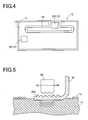
- Fig. 4 shows an example of the board 10 used in the present embodiment.
- the Al wiring layer 12 On the surface of the ceramic substrate 11 is formed the Al wiring layer 12, whose shape is determined according to each configuration of the components to be bonded thereto.
- the Ni layer 13 is partially formed on the wiring layer 12, excepting the exposing region 32 corresponding to the place where the end portion 30a of the bus bar 30 is bonded.
- This exposing region 32 covers a range in which at least the end portion 30a contacts with the A1 wiring layer 12 and a range which does not interfere with a place where the semiconductor device 20 is bonded by solder 21.
- This exposing region 32 is preferably determined to have an appropriate margin in consideration of variations or tolerances of the contact area of the end portion 30a. In this exposing region 32, the Al wiring layer 12 constructing an under layer thereof is visible.
- This manufacturing method includes a wiring layer forming process, a partially plating process, a device bonding process, and an ultrasonic bonding process, which are executed in this order.
- the wiring layer forming process is a process for forming the wiring layer 12 of A1 onto the ceramic substrate 11. This process is the same as a conventional process.
- the partially plating process is a process for applying partial Ni plating onto the wiring layer 12.
- Ni plating is applied after providing a mask on only the area corresponding to the exposing region 32, that is, the contact area of the end portion 30a and the surrounding region around it. In this manner, the exposing region 32 remains uncoated with Ni.
- another way may be adopted, in which Ni plating is applied to all over the wiring layer 12, a mask is added to an area excepting the exposing region 32, that is, to the coating region 33, and then the plated layer of an unmasked area is removed by etching or the like. In this manner, the Ni layer plated to the exposing region 32 is removed by etching. In either case, the mask is removed after all operations of this process stage. Thus, the board 10 shown in Fig. 4 is completely formed.
- the subsequent device bonding process is a process for soldering each semiconductor device 20 onto the board 10 at each predetermined place.
- the Ni layer 13 has been formed as above. Since Ni is a metal having good solder wetability, the semiconductor device 20 can easily be soldered onto the Ni layer 13 with sufficient bonding strength. This process is the same as a conventional process.
- the ultrasonic bonding process is a process for ultrasonically bonding the bus bar 30 to the wiring layer 12.
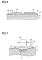
- the end portion 30a of the bus bar 30 is placed on the substrate 10 at a predetermined place, and an ultrasonic horn 40 is set in contact with the end portion 30a from above. At this time, the lower surface in the figure of the end portion 30a is held in direct contact with the Al layer forming the wiring layer 12.
- the ultrasonic horn 40 is actuated to vibrate, its vibrational energy is appropriately transmitted to the end portion 30a and, through this end portion 30a, to the wiring layer 12.
- the end portion 30a can adequately be bonded to the wiring layer 12 with strong bonding strength because an oxide film resulting from oxidation of aluminium will cause no trouble in the ultrasonic bonding method.
- the ultrasonic bonding method needs no heating.
- vibration of the housing or stress thereto will be transmitted to the externally leading conductor.
- Such vibration or stress is likely to be transmitted directly to the bonded place without mitigation because the bus bar 30 generally has high rigidity.
- the ultrasonic bonding provides higher bonding strength than the solder bonding. According to the present embodiment, therefore, the bus bar 30 can be bonded so securely as to stand against the vibration or stress transmitted thereto.
- the circuit device 1 in which both of the semiconductor devices 20 and bus bars 30 are appropriately bonded can be fabricated.
- the semiconductor devices 20 and the bus bars 30 are bonded in the order that the device bonding process is performed before the ultrasonic bonding process. Alternatively, these processes may be performed in reverse order from above.
- results for evaluation test executed by the inventors of the present invention are shown below.
- the test was made to bond the bus bar 30 having the end portion 30a whose contact area with the A1 layer was about 11 mm 2 .
- the bonding conditions of the ultrasonic bonding were a frequency of 21 kHz, an amplitude of 44 ⁇ m, a pressing force of 160N, and a time of 1.2 seconds.
- the bonded part of the end portion 30a bonded in this bonding test was peeled away from the A1 layer and the area of the actually bonded part was checked. It was found that almost all the contact area of the end portion 30a was bonded to the A1 layer and hence that the area of the bonded part was enough to provide sufficient bonding strength. In a multipoint test, even a lowest result was superior to a best result obtained in a test using the above mentioned conventional technique. Further, the required level of bonding quality was fully achieved.
- the Ni layer 13 is plated on the surface of the board 10 having the A1 wiring layer 12, excepting the exposing region 32 to which the bus bar is to be bonded. Accordingly, each semiconductor device 20 can easily be bonded, with solder 21, to the coated region 33 in which the Ni layer 13 is formed. On the other hand, it is easy to ultrasonically bond the bus bar 30 to the exposing region 32 exposing the Al wiring layer 12. It is further possible to obtain a sufficient bonded area and bonding strength. Consequently, the circuit device 1 can be arranged so that the semiconductor devices 20 and the bus bars 30 are bonded respectively with sufficient bonding strength to the board 10 made of ceramics as a major component.
- each shape of the board 10, wiring layer 12, bus bar 30, and others shown in the present embodiment is merely one example and not limited thereto.
- Al, Ni, and Cu may not be pure. While the presently preferred embodiment of the present invention has been shown and described, it is to be understood that this disclosure is for the purpose of illustration and that various changes and modifications may be made without departing from the scope of the invention as set forth in the appended claims.
Landscapes
- Engineering & Computer Science (AREA)
- Microelectronics & Electronic Packaging (AREA)
- Manufacturing & Machinery (AREA)
- Manufacturing Of Printed Wiring (AREA)
- Electric Connection Of Electric Components To Printed Circuits (AREA)
- Pressure Welding/Diffusion-Bonding (AREA)
Abstract
Description
- The present invention relates to a circuit device in which a semiconductor device and a bus bar are bonded to a ceramic based board, and a manufacturing method thereof, and more particularly to a circuit device including a ceramic substrate, on a surface of which a wiring layer made of aluminium as a major component is formed, and a manufacturing method thereof.
- Heretofore, there is a circuit device in which a plurality of semiconductor devices and bus bars are mounted on a board. An example of such board may include a ceramic substrate having ceramic material as a base body. For example, a board, called "DBA (Direct Bonded Aluminum) board", in which an aluminium (Al) wiring layer is formed on both surfaces of an aluminium nitride (A1N) substrate is used in many cases. In order to bond the semiconductor device and others to the board by soldering, for example, the surface of the Al layer is typically coated with nickel (Ni) plating or other material plating.
- In a power module using the above board, however, thermal shock attributable to heat generation of a semiconductor chip may be added to a solder layer during use. Accordingly, the solder layer may be cracked and the board is likely to be warped or broken due to a difference in coefficient of thermal expansion. In
Japanese unexamined patent application publication No. 11-346037(1999 - In
Japanese unexamined patent application publication No. 2002-9190 - However, the above mentioned conventional techniques have the following problems. The technique of the '037 publication needs the ceramic board bonded to the bus bar, thus leading to an increase in the number of parts and a complicated manufacturing process. In addition, a bonded part between the bus bar and the ceramic board may cause a thermal problem as in the above case.
- The technique of the '190 publication can adequately avoid such problem that the bonded part is broken by heat, as compared with the case using the thermal bonding technique. Hence, the inventors of the present invention have tried to ultrasonically bond a copper bus bar to a typical DBA board coated with Ni plating. However, it can be hardly said that sufficient bonding property could be obtained. To find a cause thereof, the inventors examined the bonded part by peeling the bus bar from the substrate. As a result thereof, it was found that the bus bar and the substrate were not appropriately bonded to each other at a central portion of the bonded part. The reason thereof will be explained below.
- A
board 100 of a conventional circuit device subjected to the above inspection has a structure, as shown in Fig. 6, that awiring layer 12 made of aluminium (A1) is formed on the surface of aceramic substrate 11 made of A1N and others as main components, and further aNi layer 13 is plated on thewiring layer 12. Asemiconductor device 20 is bonded to theboard 100 withsolder 21. Fig. 6 shows a state of theboard 100 on which thebus bar 30 is yet to be bonded. - Then, an
ultrasonic horn 40 is set in contact with thebus bar 30 placed on theboard 100 to perform ultrasonic bonding. At this stage, as shown in Fig. 7, thebus bar 30 is vibrated by theultrasonic horn 40. The Al layer forming thewiring layer 12 of theboard 100 is very soft as compared with theNi layer 13. It was accordingly found that vibration for ultrasonic bonding caused so large deformation of the A1 layer that theNi layer 13 got stuck into thewiring layer 12. Specifically, energy of vibration could not appropriately be transmitted to a contact surface, i.e., theNi layer 13. - Actually, the
bus bar 30 and theboard 100 were not appropriately bonded each other within most part of the bonded area as shown in Fig. 7. In the central portion of the bonded area, specifically, thebus bar 30 merely overlapped theNi layer 13 without being bonded thereto. At an end portion of the bonded area, on the other hand, theNi layer 13 was broken and pushed away, so that thebus bar 30 was bonded to the Alwiring layer 12. Thus, the actual area of the bonded part was small, which could not provide sufficient bonding strength. - The present invention has been made in view of the above circumstances and has an object to provide a circuit device in which a semiconductor device and a bus bar bonded to a ceramic board with sufficient bonding strength, and a manufacturing method thereof. Additional objects and advantages of the invention will be set forth in part in the description which follows and in part will be obvious from the description, or may be learned by practice of the invention. The objects and advantages of the invention may be realized and attained by means of the instrumentalities and combinations particularly pointed out in the appended claims.
- To achieve the purpose of the invention, there is provided a circuit device in which a functional device and an externally leading conductor are mounted, comprising: a substrate; a wiring layer provided on the substrate and electrically connected to the functional device and to the externally leading conductor; and a coating metal layer formed on a part of the wiring layer to provide a coated region in which the wiring layer is coated and an exposing region in which the wiring layer is exposed; wherein the functional device is connected onto the coating metal layer within the coated region, and the externally leading conductor is bonded to a part of the wiring layer within the exposing region.
- According to another aspect of the present invention, there is provided A method of manufacturing a circuit device in which a functional device and an externally leading conductor are mounted, the method comprising the steps of: partially forming a coating metal layer onto a wiring layer formed on a substrate, thereby providing a coated region in which the wiring layer is coated and an exposing region in which the wiring layer is exposed; connecting the functional device onto the coating metal layer within the coated region; and bonding the externally leading conductor to a portion of the wiring layer within the exposing region.
- According to the present invention, the functional device and the externally leading conductor are electrically connected to the board including a substrate made of ceramics or the like provided with a wiring layer formed thereon. The functional device is connected to the coated region in which the wiring layer is coated with the coating metal layer. On the other hand, the externally leading conductor is directly connected to the wiring layer within the exposing region in which the wiring layer is uncoated with the coating metal layer and thus exposed. Accordingly, an appropriate bonding technique can be selected for each bonding part. For example, as for an Al wiring layer, the externally leading conductor is bonded to the wiring layer by ultrasonic bonding, so that they can be bonded with sufficient bonding strength. Further, as for the coating metal layer made of nickel (Ni), copper (Cu), or other material having solder wetability superior to Al, the functional device is bonded to the coating metal layer by soldering, so that they can be bonded with sufficient bonding strength.
- According to the circuit device and its manufacturing method of the present invention, the semiconductor device and the bus bar can be bonded to the ceramic board with sufficient bonding strength.
- The accompanying drawings, which are incorporated in and constitute a part of this specification illustrate an embodiment of the invention and, together with the description, serve to explain the objects, advantages and principles of the invention.
In the drawings, - Fig. 1 is a sectional view of part of a circuit device in the present embodiment;
- Fig. 2 is a plan view of part of the circuit device;
- Fig. 3 is an enlarged sectional view of part of the circuit device;
- Fig. 4 is an explanatory view showing a ceramic board used in the circuit device;
- Fig. 5 is an explanatory view showing a bonding method in the present embodiment;
- Fig. 6 is an explanatory view showing a conventional bonding method; and
- Fig. 7 is an explanatory view showing a bonded state by the conventional bonding method.
- A detailed description of a preferred embodiment of the present invention will now be given referring to the accompanying drawings. In the present embodiment, the present invention is applied to a circuit device in which a semiconductor device and a bus bar are bonded to a ceramic board.
- A circuit device 1 in the present embodiment, as shown in Fig. 1 (a sectional view) and Fig. 2 (a plan view), is structured such that semiconductor devices 20 (IGBT or the like) and
bus bars 30 which are bonded to aboard 10. Thisboard 10 includes aceramic substrate 11 made of A1N or the like as a major component, awiring layer 12 made of Al formed on both surfaces of theceramic substrate 11, and anNi layer 13 corresponding to a coating metal layer plated on a surface of thewiring layer 12. As an alternative to theNi layer 13, a Cu-plated layer may be adopted. On an upper surface (in the figure) of theboard 10, thesemiconductor device 20 is bonded bysolder 21. - The
bus bar 30 corresponds to an externally leading conductor, which is formed of a copper plate in bent shape. Only anend portion 30a thereof is bonded to theboard 10. Abase portion 30b is supported by ahousing 31 in spaced relation to theboard 10. This arrangement can achieve a smaller area of theboard 10 in plan view than conventional one. Thehousing 31 is fixed to aheat radiation board 23 to maintain its entire strength and shape. Herein, Fig. 1 shows about a half part of the entire circuit device 1 in a right-and-left direction in the figure. The circuit device 1 actually includes the other half part (on the right side of the illustrated half part) provided with components substantially symmetrical to those shown in Fig. 1. Fig. 2 shows only a little part of the circuit device 1 in plan view. Practically, a plurality of theboards 10 each including a substantially identical structure or symmetrical structure are arranged continuously lengthwise and breadthwise, which are bonded to a single heat radiation board 23 (omitted from Fig. 2). - Fig. 3 is an enlarged view of a part of the circuit device 1 shown in Fig. 1. As shown in Figs. 2 and 3, the
Ni layer 13 is not plated on and around a portion of theboard 10 bonded with theend portion 30a of thebus bar 30. Specifically, an exposingregion 32 in which Al of thewiring layer 12 is exposed is provided around theend portion 30a. Theend portion 30a is directly bonded to the A1 of thewiring layer 12 within the exposingregion 32. Thewiring layer 12 other than the exposingregion 32 is coated with theNi layer 13. In other words, theboard 10 in the present embodiment is provided with the exposingregion 32 in which A1 of thewiring layer 12 is exposed and acoated region 33 in which A1 of thewiring layer 12 is coated with theNi layer 13. - Aluminum is apt to be oxidized when exposed, forming an oxide film, so that the bonding by
solder 21 is rather difficult. On the other hand, the ultrasonic bonding of thebus bar 30 to thewiring layer 12 with theNi layer 13 has a problem with the bonding property as mentioned above. To avoid such problems, the circuit device 1 in the present embodiment is arranged such that a portion of thewiring layer 12 to which thesemiconductor device 20 is bonded by thesolder 21 is coated with theNi layer 13, whereas remaining portion to which thebus bar 30 is bonded by the ultrasonic bonding is uncoated with theNi layer 13. - Fig. 4 shows an example of the
board 10 used in the present embodiment. On the surface of theceramic substrate 11 is formed theAl wiring layer 12, whose shape is determined according to each configuration of the components to be bonded thereto. TheNi layer 13 is partially formed on thewiring layer 12, excepting the exposingregion 32 corresponding to the place where theend portion 30a of thebus bar 30 is bonded. This exposingregion 32 covers a range in which at least theend portion 30a contacts with theA1 wiring layer 12 and a range which does not interfere with a place where thesemiconductor device 20 is bonded bysolder 21. This exposingregion 32 is preferably determined to have an appropriate margin in consideration of variations or tolerances of the contact area of theend portion 30a. In this exposingregion 32, theAl wiring layer 12 constructing an under layer thereof is visible. - Next, the manufacturing method of the circuit device 1 in the present embodiment will be explained below. This manufacturing method includes a wiring layer forming process, a partially plating process, a device bonding process, and an ultrasonic bonding process, which are executed in this order. Firstly, the wiring layer forming process is a process for forming the
wiring layer 12 of A1 onto theceramic substrate 11. This process is the same as a conventional process. - The partially plating process is a process for applying partial Ni plating onto the
wiring layer 12. In this partially plating method, for example, Ni plating is applied after providing a mask on only the area corresponding to the exposingregion 32, that is, the contact area of theend portion 30a and the surrounding region around it. In this manner, the exposingregion 32 remains uncoated with Ni. Alternatively, another way may be adopted, in which Ni plating is applied to all over thewiring layer 12, a mask is added to an area excepting the exposingregion 32, that is, to thecoating region 33, and then the plated layer of an unmasked area is removed by etching or the like. In this manner, the Ni layer plated to the exposingregion 32 is removed by etching. In either case, the mask is removed after all operations of this process stage. Thus, theboard 10 shown in Fig. 4 is completely formed. - The subsequent device bonding process is a process for soldering each
semiconductor device 20 onto theboard 10 at each predetermined place. In the place where eachsemiconductor device 20 is to be soldered, theNi layer 13 has been formed as above. Since Ni is a metal having good solder wetability, thesemiconductor device 20 can easily be soldered onto theNi layer 13 with sufficient bonding strength. This process is the same as a conventional process. - The ultrasonic bonding process is a process for ultrasonically bonding the
bus bar 30 to thewiring layer 12. Theend portion 30a of thebus bar 30 is placed on thesubstrate 10 at a predetermined place, and anultrasonic horn 40 is set in contact with theend portion 30a from above. At this time, the lower surface in the figure of theend portion 30a is held in direct contact with the Al layer forming thewiring layer 12. When theultrasonic horn 40 is actuated to vibrate, its vibrational energy is appropriately transmitted to theend portion 30a and, through thisend portion 30a, to thewiring layer 12. As shown in Fig. 5, theend portion 30a can adequately be bonded to thewiring layer 12 with strong bonding strength because an oxide film resulting from oxidation of aluminium will cause no trouble in the ultrasonic bonding method. - Furthermore, there is no possibility of affecting the
solder 21, 22 and thewiring layer 12, since the ultrasonic bonding method needs no heating. The other end of thebus bar 30, i.e., the end other than the bonded end portion with thewiring layer 12, is often connected directly to a housing containing the circuit device 1. Thus, vibration of the housing or stress thereto will be transmitted to the externally leading conductor. Such vibration or stress is likely to be transmitted directly to the bonded place without mitigation because thebus bar 30 generally has high rigidity. In general, the ultrasonic bonding provides higher bonding strength than the solder bonding. According to the present embodiment, therefore, thebus bar 30 can be bonded so securely as to stand against the vibration or stress transmitted thereto. - According to the manufacturing method in the present embodiment, as described above, the circuit device 1 in which both of the
semiconductor devices 20 andbus bars 30 are appropriately bonded can be fabricated. In the explanation of the present embodiment, thesemiconductor devices 20 and the bus bars 30 are bonded in the order that the device bonding process is performed before the ultrasonic bonding process. Alternatively, these processes may be performed in reverse order from above. - Results for evaluation test executed by the inventors of the present invention are shown below. Herein, the test was made to bond the
bus bar 30 having theend portion 30a whose contact area with the A1 layer was about 11 mm2. The bonding conditions of the ultrasonic bonding were a frequency of 21 kHz, an amplitude of 44 µm, a pressing force of 160N, and a time of 1.2 seconds. The bonded part of theend portion 30a bonded in this bonding test was peeled away from the A1 layer and the area of the actually bonded part was checked. It was found that almost all the contact area of theend portion 30a was bonded to the A1 layer and hence that the area of the bonded part was enough to provide sufficient bonding strength. In a multipoint test, even a lowest result was superior to a best result obtained in a test using the above mentioned conventional technique. Further, the required level of bonding quality was fully achieved. - According to the circuit device 1 of the present invention, as explained above in detail, the
Ni layer 13 is plated on the surface of theboard 10 having theA1 wiring layer 12, excepting the exposingregion 32 to which the bus bar is to be bonded. Accordingly, eachsemiconductor device 20 can easily be bonded, withsolder 21, to thecoated region 33 in which theNi layer 13 is formed. On the other hand, it is easy to ultrasonically bond thebus bar 30 to the exposingregion 32 exposing theAl wiring layer 12. It is further possible to obtain a sufficient bonded area and bonding strength. Consequently, the circuit device 1 can be arranged so that thesemiconductor devices 20 and the bus bars 30 are bonded respectively with sufficient bonding strength to theboard 10 made of ceramics as a major component. - The present invention may be embodied in other specific forms without departing from the spirit or essential characteristics thereof. For instance, each shape of the
board 10,wiring layer 12,bus bar 30, and others shown in the present embodiment is merely one example and not limited thereto. Al, Ni, and Cu may not be pure. While the presently preferred embodiment of the present invention has been shown and described, it is to be understood that this disclosure is for the purpose of illustration and that various changes and modifications may be made without departing from the scope of the invention as set forth in the appended claims.
Claims (12)
- A circuit device (1) in which a functional device and an externally leading conductor (30) are mounted, comprising:a substrate (11);a wiring layer (12) provided on the substrate (11) and electrically connected to the functional device and to the externally leading conductor (30); anda coating metal layer (13) formed on a part of the wiring layer (12) to provide a coated region in which the wiring layer (12) is coated and an exposing region in which the wiring layer (12) is exposed;wherein the functional device is connected onto the coating metal layer (13) within the coated region, andthe externally leading conductor (30) is bonded to a part of the wiring layer (12) within the exposing region.
- The circuit device according to claim 1, wherein the wiring layer (12) is made of aluminium.
- The circuit device according to claim 2, wherein the coating metal layer (13) is made of metal having solder wetability superior to aluminium.
- The circuit device according to claim 3, wherein the functional device is connected onto the coating metal layer (13) within the coated region through solder.
- The circuit device according to claim 3, wherein the coating metal layer (13) is made of nickel or copper.
- The circuit device according to claim 1, wherein the externally leading conductor (30) is bonded to the wiring layer (12) within the exposing region by ultrasonic bonding.
- A method of manufacturing a circuit device in which a functional device and an externally leading conductor (30) are mounted, the method comprising the steps of:partially forming a coating metal layer (13) onto a wiring layer (12) formed on a substrate, thereby providing a coated region in which the wiring layer (12) is coated and an exposing region in which the wiring layer (12) is exposed;connecting the functional device onto the coating metal layer (13) within the coated region; andbonding the externally leading conductor (30) to a portion of the wiring layer (12) within the exposing region.
- The manufacturing method of the circuit device, according to claim 7, wherein the wiring layer (12) is made of aluminium.
- The manufacturing method of the circuit device, according to claim 8, wherein the coating metal layer (13) is made of metal having solder wetability superior to aluminium.
- The manufacturing method of the circuit device, according to claim 9, wherein the functional device is connected onto the coating metal layer (13) within the coated region through solder.
- The manufacturing method of the circuit device, according to claim 9, the coating metal layer (13) is made of nickel or copper.
- The manufacturing method of the circuit device, according to claim 7, wherein the externally leading conductor (30) is bonded onto the wiring layer (12) within the exposing region by ultrasonic bonding.
Applications Claiming Priority (1)
| Application Number | Priority Date | Filing Date | Title |
|---|---|---|---|
| JP2005098648A JP2006278913A (en) | 2005-03-30 | 2005-03-30 | Circuit device and manufacturing method thereof |
Publications (2)
| Publication Number | Publication Date |
|---|---|
| EP1711040A1 true EP1711040A1 (en) | 2006-10-11 |
| EP1711040B1 EP1711040B1 (en) | 2007-09-12 |
Family
ID=36617605
Family Applications (1)
| Application Number | Title | Priority Date | Filing Date |
|---|---|---|---|
| EP20060004265 Expired - Lifetime EP1711040B1 (en) | 2005-03-30 | 2006-03-02 | Circuit device and manufacturing method thereof |
Country Status (6)
| Country | Link |
|---|---|
| US (1) | US7446406B2 (en) |
| EP (1) | EP1711040B1 (en) |
| JP (1) | JP2006278913A (en) |
| KR (1) | KR100729249B1 (en) |
| CN (1) | CN100390989C (en) |
| DE (1) | DE602006000104T2 (en) |
Cited By (4)
| Publication number | Priority date | Publication date | Assignee | Title |
|---|---|---|---|---|
| WO2009127179A1 (en) * | 2008-04-15 | 2009-10-22 | Conti Temic Microelectonic Gmbh | Method for producing and assembly of a power module |
| WO2012049087A2 (en) | 2010-10-13 | 2012-04-19 | Abb Research Ltd | Semiconductor module and method of manufacturing a semiconductor module |
| WO2014035314A1 (en) * | 2012-08-29 | 2014-03-06 | Inco Innovation | Power chain on a circuit board |
| EP2613352A3 (en) * | 2012-01-05 | 2015-12-23 | Ixys Corporation | Discrete power transistor package having solderless dbc to leadframe attach |
Families Citing this family (23)
| Publication number | Priority date | Publication date | Assignee | Title |
|---|---|---|---|---|
| US7799273B2 (en) | 2004-05-06 | 2010-09-21 | Smp Logic Systems Llc | Manufacturing execution system for validation, quality and risk assessment and monitoring of pharmaceutical manufacturing processes |
| US7444197B2 (en) | 2004-05-06 | 2008-10-28 | Smp Logic Systems Llc | Methods, systems, and software program for validation and monitoring of pharmaceutical manufacturing processes |
| AU2006212875B2 (en) * | 2005-02-08 | 2011-06-02 | Dyno Nobel Inc. | Delay units and methods of making the same |
| JP4965242B2 (en) * | 2006-12-27 | 2012-07-04 | 株式会社ティラド | Manufacturing method of aluminum heat sink |
| JP5102497B2 (en) * | 2007-01-19 | 2012-12-19 | Dowaメタルテック株式会社 | Method for manufacturing metal-ceramic bonded circuit board |
| JP2008277438A (en) * | 2007-04-26 | 2008-11-13 | Ricoh Microelectronics Co Ltd | Electronic component, substrate, and electronic component and substrate manufacturing method |
| JP4935735B2 (en) * | 2008-03-26 | 2012-05-23 | トヨタ自動車株式会社 | Bus bar and manufacturing method thereof |
| JP2010239033A (en) * | 2009-03-31 | 2010-10-21 | Honda Motor Co Ltd | Semiconductor device and manufacturing method thereof |
| WO2011036307A1 (en) | 2009-09-28 | 2011-03-31 | Abb Technology Ag | Circuit arrangement and manufacturing method thereof |
| WO2011112647A1 (en) | 2010-03-09 | 2011-09-15 | Dyno Nobel Inc. | Sealer elements, detonators containing the same, and methods of making |
| JP2013235882A (en) | 2012-05-07 | 2013-11-21 | Mitsubishi Electric Corp | Semiconductor device |
| US8716864B2 (en) * | 2012-06-07 | 2014-05-06 | Ixys Corporation | Solderless die attach to a direct bonded aluminum substrate |
| WO2014049740A1 (en) * | 2012-09-26 | 2014-04-03 | トヨタ自動車株式会社 | Electric component |
| US8987911B2 (en) * | 2012-12-31 | 2015-03-24 | Ixys Corporation | Silver-to-silver bonded IC package having two ceramic substrates exposed on the outside of the package |
| DE102013221090A1 (en) * | 2013-10-17 | 2015-04-23 | Continental Teves Ag & Co. Ohg | Electronic control device and method for the arrangement and electrical connection of electronic components on a circuit carrier |
| US9312231B2 (en) * | 2013-10-31 | 2016-04-12 | Freescale Semiconductor, Inc. | Method and apparatus for high temperature semiconductor device packages and structures using a low temperature process |
| JP2015201505A (en) * | 2014-04-07 | 2015-11-12 | 三菱電機株式会社 | semiconductor device |
| JP6468984B2 (en) * | 2015-10-22 | 2019-02-13 | 三菱電機株式会社 | Semiconductor device |
| JP6665664B2 (en) * | 2016-04-27 | 2020-03-13 | 富士電機株式会社 | Semiconductor device and manufacturing method thereof |
| KR102239209B1 (en) * | 2018-10-24 | 2021-04-12 | 대산전자(주) | Plating method and plated metal |
| JP7528481B2 (en) * | 2020-03-18 | 2024-08-06 | 富士電機株式会社 | Semiconductor module and manufacturing method thereof |
| CN111751272B (en) | 2020-07-03 | 2021-09-07 | 北京理工大学 | A method of ultrasonic testing and tensile calibration test for bond strength grades |
| CN112583210A (en) * | 2020-12-28 | 2021-03-30 | 上海大郡动力控制技术有限公司 | Low stray inductance busbar structure for power module |
Citations (6)
| Publication number | Priority date | Publication date | Assignee | Title |
|---|---|---|---|---|
| JPH11346037A (en) * | 1998-05-29 | 1999-12-14 | Kyocera Corp | Heat dissipation board |
| US6166937A (en) * | 1998-06-02 | 2000-12-26 | Hitachi Ltd. | Inverter device with cooling arrangement therefor |
| JP2002009190A (en) * | 2000-06-16 | 2002-01-11 | Ngk Spark Plug Co Ltd | Ceramic substrate and method of manufacturing the same |
| EP1187198A2 (en) * | 2000-09-04 | 2002-03-13 | Dowa Mining Co., Ltd. | Metal-ceramic circuit board and manufacturing method thereof |
| JP2003060129A (en) * | 2001-08-09 | 2003-02-28 | Denki Kagaku Kogyo Kk | Circuit board and partial plating method for circuit board |
| EP1416533A2 (en) * | 2002-10-29 | 2004-05-06 | Ixys Corporation | Power device and direct aluminium bonded substrate thereof |
Family Cites Families (11)
| Publication number | Priority date | Publication date | Assignee | Title |
|---|---|---|---|---|
| JPS5386576A (en) * | 1977-01-10 | 1978-07-31 | Nec Corp | Package for semiconductor element |
| JPH0620998B2 (en) * | 1988-01-20 | 1994-03-23 | 株式会社豊田自動織機製作所 | Spreader alignment device |
| JP2963289B2 (en) * | 1992-11-30 | 1999-10-18 | ユニ・チャーム株式会社 | Surface sheet for body fluid absorbent articles |
| JP3524360B2 (en) | 1997-12-26 | 2004-05-10 | 株式会社東芝 | Semiconductor device and manufacturing method thereof |
| JP2000232189A (en) | 1999-02-10 | 2000-08-22 | Toshiba Corp | Semiconductor device |
| JP2002164461A (en) | 2000-11-24 | 2002-06-07 | Kyocera Corp | Ceramic circuit board |
| JP2002231882A (en) * | 2001-02-06 | 2002-08-16 | Mitsubishi Electric Corp | Semiconductor device |
| US6787706B2 (en) * | 2001-02-21 | 2004-09-07 | Kyocera Corporation | Ceramic circuit board |
| DE10157362B4 (en) * | 2001-11-23 | 2006-11-16 | Infineon Technologies Ag | Power module and method for its production |
| JP2003188310A (en) | 2001-12-18 | 2003-07-04 | Denki Kagaku Kogyo Kk | Method of manufacturing circuit board with electrode terminals |
| JP3891838B2 (en) * | 2001-12-26 | 2007-03-14 | 株式会社ルネサステクノロジ | Semiconductor device and manufacturing method thereof |
-
2005
- 2005-03-30 JP JP2005098648A patent/JP2006278913A/en active Pending
-
2006
- 2006-03-02 DE DE200660000104 patent/DE602006000104T2/en not_active Expired - Fee Related
- 2006-03-02 EP EP20060004265 patent/EP1711040B1/en not_active Expired - Lifetime
- 2006-03-27 US US11/388,987 patent/US7446406B2/en not_active Expired - Fee Related
- 2006-03-28 CN CNB2006100585006A patent/CN100390989C/en not_active Expired - Fee Related
- 2006-03-29 KR KR20060028324A patent/KR100729249B1/en not_active Expired - Fee Related
Patent Citations (6)
| Publication number | Priority date | Publication date | Assignee | Title |
|---|---|---|---|---|
| JPH11346037A (en) * | 1998-05-29 | 1999-12-14 | Kyocera Corp | Heat dissipation board |
| US6166937A (en) * | 1998-06-02 | 2000-12-26 | Hitachi Ltd. | Inverter device with cooling arrangement therefor |
| JP2002009190A (en) * | 2000-06-16 | 2002-01-11 | Ngk Spark Plug Co Ltd | Ceramic substrate and method of manufacturing the same |
| EP1187198A2 (en) * | 2000-09-04 | 2002-03-13 | Dowa Mining Co., Ltd. | Metal-ceramic circuit board and manufacturing method thereof |
| JP2003060129A (en) * | 2001-08-09 | 2003-02-28 | Denki Kagaku Kogyo Kk | Circuit board and partial plating method for circuit board |
| EP1416533A2 (en) * | 2002-10-29 | 2004-05-06 | Ixys Corporation | Power device and direct aluminium bonded substrate thereof |
Non-Patent Citations (3)
| Title |
|---|
| PATENT ABSTRACTS OF JAPAN vol. 2000, no. 03 30 March 2000 (2000-03-30) * |
| PATENT ABSTRACTS OF JAPAN vol. 2002, no. 05 3 May 2002 (2002-05-03) * |
| PATENT ABSTRACTS OF JAPAN vol. 2003, no. 06 3 June 2003 (2003-06-03) * |
Cited By (13)
| Publication number | Priority date | Publication date | Assignee | Title |
|---|---|---|---|---|
| WO2009127179A1 (en) * | 2008-04-15 | 2009-10-22 | Conti Temic Microelectonic Gmbh | Method for producing and assembly of a power module |
| WO2012049087A2 (en) | 2010-10-13 | 2012-04-19 | Abb Research Ltd | Semiconductor module and method of manufacturing a semiconductor module |
| WO2012049087A3 (en) * | 2010-10-13 | 2012-06-21 | Abb Research Ltd | Semiconductor module and method of manufacturing a semiconductor module |
| CN103155131A (en) * | 2010-10-13 | 2013-06-12 | Abb研究有限公司 | Semiconductor module and method of manufacturing a semiconductor module |
| EP3544053A1 (en) * | 2012-01-05 | 2019-09-25 | Ixys Corporation | Discrete power transistor package having solderless dbc to leadframe attach |
| EP2613352A3 (en) * | 2012-01-05 | 2015-12-23 | Ixys Corporation | Discrete power transistor package having solderless dbc to leadframe attach |
| US10720376B2 (en) | 2012-01-05 | 2020-07-21 | Littelfuse, Inc. | Discrete power transistor package having solderless DBC to leadframe attach |
| EP3940770A1 (en) * | 2012-01-05 | 2022-01-19 | Littelfuse, Inc. | Discrete power transistor package having solderless dbc to leadframe attach |
| US11387162B2 (en) | 2012-01-05 | 2022-07-12 | Littelfuse, Inc. | Discrete power transistor package having solderless DBC to leadframe attach |
| GB2509002A (en) * | 2012-08-29 | 2014-06-18 | Inco Innovation | Power chain on a circuit board |
| GB2509002B (en) * | 2012-08-29 | 2014-09-10 | Inco Innovation | Power chain on a circuit board |
| US9545007B2 (en) | 2012-08-29 | 2017-01-10 | One Inventor Sweden AB | Power chain on a circuit board |
| WO2014035314A1 (en) * | 2012-08-29 | 2014-03-06 | Inco Innovation | Power chain on a circuit board |
Also Published As
| Publication number | Publication date |
|---|---|
| JP2006278913A (en) | 2006-10-12 |
| US7446406B2 (en) | 2008-11-04 |
| KR100729249B1 (en) | 2007-06-15 |
| DE602006000104T2 (en) | 2008-06-12 |
| DE602006000104D1 (en) | 2007-10-25 |
| US20060220216A1 (en) | 2006-10-05 |
| EP1711040B1 (en) | 2007-09-12 |
| CN1841726A (en) | 2006-10-04 |
| KR20060106743A (en) | 2006-10-12 |
| CN100390989C (en) | 2008-05-28 |
Similar Documents
| Publication | Publication Date | Title |
|---|---|---|
| EP1711040B1 (en) | Circuit device and manufacturing method thereof | |
| US5757071A (en) | C4 substrate contact pad which has a layer of Ni-B plating | |
| US5029386A (en) | Hierarchical tape automated bonding method | |
| KR100531393B1 (en) | Semiconductor device and manufacturing method of the same | |
| US5876859A (en) | Direct metal bonding | |
| EP1868244B1 (en) | Semiconductor device | |
| JP4283514B2 (en) | Electronic circuit equipment | |
| JPH01235170A (en) | Micro i/o pin and its manufacture | |
| JPH0636852A (en) | Method for connecting terminal to printed wiring board | |
| JPH09232499A (en) | Semiconductor device | |
| JP4244235B2 (en) | Electronic circuit equipment | |
| JP2968051B2 (en) | Chip interconnect carrier and method for mounting a spring contact on a semiconductor device | |
| JPH04212277A (en) | Method of connecting terminal to printed wiring board | |
| JP3297959B2 (en) | Semiconductor device | |
| JPH0233960A (en) | Semiconductor device | |
| JPH08255851A (en) | Semiconductor package | |
| JPH08264910A (en) | Manufacture of printed wiring board with heat sink and method for mounting high-power component on the board | |
| JPS63285960A (en) | Conductor pin for semiconductor mounting substrate and manufacture thereof | |
| JP3061017B2 (en) | Mounting structure of integrated circuit device and mounting method thereof | |
| JP2000164757A (en) | Package for housing semiconductor element and its mounting structure | |
| JP3563846B2 (en) | Method of manufacturing lead frame member for BGA type resin-sealed semiconductor device | |
| JPH05326814A (en) | Lead frame for mounting electronic circuit device | |
| JPS6317547A (en) | Semiconductor device | |
| JP2001127104A (en) | Semiconductor element mounting method | |
| JPH0964092A (en) | Device mounting structure |
Legal Events
| Date | Code | Title | Description |
|---|---|---|---|
| PUAI | Public reference made under article 153(3) epc to a published international application that has entered the european phase |
Free format text: ORIGINAL CODE: 0009012 |
|
| 17P | Request for examination filed |
Effective date: 20060302 |
|
| AK | Designated contracting states |
Kind code of ref document: A1 Designated state(s): AT BE BG CH CY CZ DE DK EE ES FI FR GB GR HU IE IS IT LI LT LU LV MC NL PL PT RO SE SI SK TR |
|
| AX | Request for extension of the european patent |
Extension state: AL BA HR MK YU |
|
| GRAP | Despatch of communication of intention to grant a patent |
Free format text: ORIGINAL CODE: EPIDOSNIGR1 |
|
| RIN1 | Information on inventor provided before grant (corrected) |
Inventor name: WAKITA, SHIGERUC/O JECO CO., LTD. Inventor name: YAMAMOTO, RENC/O TOYOTA JIDOSHA K.KAISHA Inventor name: MIZUNO, TAKAHITOC/O TOYOTA JIDOSHA K.KAISHA |
|
| AKX | Designation fees paid |
Designated state(s): DE FR GB |
|
| GRAS | Grant fee paid |
Free format text: ORIGINAL CODE: EPIDOSNIGR3 |
|
| GRAA | (expected) grant |
Free format text: ORIGINAL CODE: 0009210 |
|
| AK | Designated contracting states |
Kind code of ref document: B1 Designated state(s): DE FR GB |
|
| REG | Reference to a national code |
Ref country code: GB Ref legal event code: FG4D |
|
| REF | Corresponds to: |
Ref document number: 602006000104 Country of ref document: DE Date of ref document: 20071025 Kind code of ref document: P |
|
| ET | Fr: translation filed | ||
| PLBE | No opposition filed within time limit |
Free format text: ORIGINAL CODE: 0009261 |
|
| STAA | Information on the status of an ep patent application or granted ep patent |
Free format text: STATUS: NO OPPOSITION FILED WITHIN TIME LIMIT |
|
| PGFP | Annual fee paid to national office [announced via postgrant information from national office to epo] |
Ref country code: FR Payment date: 20080311 Year of fee payment: 3 Ref country code: DE Payment date: 20080228 Year of fee payment: 3 |
|
| 26N | No opposition filed |
Effective date: 20080613 |
|
| REG | Reference to a national code |
Ref country code: FR Ref legal event code: ST Effective date: 20091130 |
|
| PG25 | Lapsed in a contracting state [announced via postgrant information from national office to epo] |
Ref country code: DE Free format text: LAPSE BECAUSE OF NON-PAYMENT OF DUE FEES Effective date: 20091001 |
|
| PG25 | Lapsed in a contracting state [announced via postgrant information from national office to epo] |
Ref country code: FR Free format text: LAPSE BECAUSE OF NON-PAYMENT OF DUE FEES Effective date: 20091123 |
|
| GBPC | Gb: european patent ceased through non-payment of renewal fee |
Effective date: 20100302 |
|
| PG25 | Lapsed in a contracting state [announced via postgrant information from national office to epo] |
Ref country code: GB Free format text: LAPSE BECAUSE OF NON-PAYMENT OF DUE FEES Effective date: 20100302 |