EP1710641B1 - Kompensierungsvorrichtung für empfangene Daten - Google Patents
Kompensierungsvorrichtung für empfangene Daten Download PDFInfo
- Publication number
- EP1710641B1 EP1710641B1 EP06005218A EP06005218A EP1710641B1 EP 1710641 B1 EP1710641 B1 EP 1710641B1 EP 06005218 A EP06005218 A EP 06005218A EP 06005218 A EP06005218 A EP 06005218A EP 1710641 B1 EP1710641 B1 EP 1710641B1
- Authority
- EP
- European Patent Office
- Prior art keywords
- data
- check
- unit
- received data
- units
- Prior art date
- Legal status (The legal status is an assumption and is not a legal conclusion. Google has not performed a legal analysis and makes no representation as to the accuracy of the status listed.)
- Ceased
Links
Images


Classifications
-
- H—ELECTRICITY
- H04—ELECTRIC COMMUNICATION TECHNIQUE
- H04L—TRANSMISSION OF DIGITAL INFORMATION, e.g. TELEGRAPHIC COMMUNICATION
- H04L1/00—Arrangements for detecting or preventing errors in the information received
- H04L1/22—Arrangements for detecting or preventing errors in the information received using redundant apparatus to increase reliability
-
- H—ELECTRICITY
- H04—ELECTRIC COMMUNICATION TECHNIQUE
- H04L—TRANSMISSION OF DIGITAL INFORMATION, e.g. TELEGRAPHIC COMMUNICATION
- H04L25/00—Baseband systems
- H04L25/02—Details ; arrangements for supplying electrical power along data transmission lines
- H04L25/03—Shaping networks in transmitter or receiver, e.g. adaptive shaping networks
- H04L25/03878—Line equalisers; line build-out devices
Definitions
- the present invention relates to a received data compensating device provided between a receiving circuit constituting a physical layer and a processing device utilizing received data and having the function of recovering the received data.
- FIG. 8 shows a diagram showing a structure of a conventional received data compensating circuit.
- a received data compensating device 100A is provided in a rear stage of a receiving IC constituting a physical layer and comprises a preprocessing unit 1 and a check unit 2 in this example.
- a received IC 200 is mounted on a printed wiring board (PWB) and the received data compensating device 100A can be properly constituted by an ASIC, an FPGA or a microcomputer.
- PWB printed wiring board
- AD485 to be an analog device can be used for the receiving IC 200.
- FIG. 8 a digital signal acquired through the receiving IC from a communicating transmission line is transferred to the received data compensating device 100.
- the preprocessing unit 1 has a filtering function and a sampling function.
- An example of the sampling circuit to be used herein is shown in FIG. 9 . This circuit has already been disclosed by the applicant based on Japanese Patent Application Laid-Open No. JP 5-130 151 A .
- the sampling circuit comprises three D-type flip-flops DFF1 to DFF3 which are cascade connected to each other, a first selector SEL1 disposed in a rear stage, a D-type flip-flop DFF4 disposed in a rear stage, a second selector SEL2 disposed in a rear stage, a D-type flip-flop DFF5 disposed in a rear stage, and serves to monitor the Q outputs of the D-type flip-flops DFF1 to DFF5 and to give switching signals S1 and S2 to the first and second selectors SEL1 and SEL2 based on the Q outputs, thereby restoring a digital signal including various noise components as shown in FIG. 10 .
- the check unit 2 serves to check a reliability of data in a frame format of a protocol such as a CRC, a parity, a stop or a coding rule or to detect an error. Furthermore, the check unit 2 also carries out decoding in the case in which a transmission line is coded. Compensated and received data (CD) passing through the check unit 2 are transmitted to the data processing device together with a check result signal S1 and are thus utilized JP.
- a protocol such as a CRC, a parity, a stop or a coding rule
- a filtering circuit included in the preprocessing circuit 1 is fixed to have one characteristic.
- a PLC system as to connect a master unit to a slave unit through a communication, therefore, there is a problem in that it is not easy to use.
- various wiring configurations such as a digichain, a multidrop, a branch and a start are mixed on a communicating path thereof.
- various transmission media electrical cables and connectors having different characteristics
- a reflecting and damping state of a signal in a transmission line is varied.
- a communication wiring specification such as a wiring length and the number of connections is more reduced than that in the case in which the wiring configuration and the transfer medium are specified into one by the same portrait.
- the present invention has been made by taking note of the conventional problems and has an object to provide a received data compensating device capable of carrying out a wide application through a single device for a transmission line including various wiring configurations and transmission media.
- a compensating device for a received data provided between a receiver circuit in a physical layer and a processing device utilizing the received data is as defined in claim 1.
- the received data obtained from the receiving circuit constituting the physical layer are processed at the same time by the preprocessing units having the filtering function and the sampling function which have different characteristics from each other. Also in the case in which the quality of the transmission line is varied variously, therefore, any of the preprocessing portions which are provided corresponds thereto so that an application to various transmission lines can be carried out by an apparatus having the same specification.
- the data selector may select and output one of the data in accordance with a preset priority when a plurality of data of the buffer units are decided to be OK based on the check result in the check unit.
- a frequency of OK is particularly increased in an optimum one of processing systems which are present through a warm-up period for a while. In consideration of the information, therefore, it is also possible to automatically search for a more proper processing system.
- the check unit may carry out the decode processing when the data are subjected to transmission line coding.
- the received data compensating device can be widely applied to a PLC system. More specifically, the present invention can enhance the degree of a line adaptation by a disposition in the rear stage of the receiving circuit constituting the physical layer for each of a master unit, a slave unit, a repeater and the like which constitute the PLC system.
- the received data obtained from the receiving circuit constituting the physical layer are processed at the same time by the preprocessing units provided in parallel with each other on an output - side thereof and having the filtering function and the sampling function which have different characteristics from each other. Irrespective of the quality and wiring configuration of the transmission line, therefore, it is possible to adapt transmission media and wiring configurations of various qualities by one receiving processing device through an adaptation of any of the processing systems to the characteristics. Thus, the usability of the receiving device of this type can be enhanced.
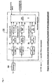
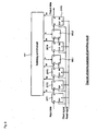
- FIG. 1 shows a diagram showing a structure of a device according to the present invention (a first embodiment);
- FIG. 1 is a diagram showing a structure of the device according to the present invention (a first embodiment).
- a received data compensating device 100 is provided in a rear stage of a receiving IC 200 constituting a physical layer. It is possible to utilize the RS485 specification for the receiving IC 200, for example. More specifically, AD485 of analog devices and the like are suitable. In this example, the receiving IC 200 is mounted on a printed wiring board.
- the received data compensating device 100 has the following structure. More specifically, the received data compensating device 100 according to the present invention comprises a plurality of preprocessing units 11, 12, ... 1N provided in parallel with each other on the output side of the receiving IC 200 and having filtering functions having different characteristics from each other and sampling functions having different characteristics from each other, a plurality of check units 21, 22, ... 2N provided in the respective rear stages of the preprocessing units 11, 12, ... 1N and serving to execute at least a reliability check of data in accordance with a frame format of a protocol, a plurality of buffer units 31, 32, ... 3N provided in the rear stages of the check units 21, 22, ... 2N and serving to store data processed in the check units, and a data - selector 4 for monitoring a check result in each of the check units 31, 32, ... 3N and selecting and outputting the data of the buffer unit having a check result of OK.
- the received data compensating device 100 comprises a plurality of preprocessing units 11, 12, ... 1N provided in parallel with each other
- a digital signal acquired from a communicating transmission line through the receiving IC 200 is then transferred to the N preprocessing units 11, 12, ... 1N provided in parallel with each other in the rear stage.
- a filter circuit for implementing the filtering function included in the preprocessing units 11, 12, ... 1N is almost identical to that described with reference to FIGs. 9 and 10 .
- Data processed by the first preprocessing unit 11, the second preprocessing unit 12, ... the Nth preprocessing unit 1N are transmitted to the first check unit 21, the second check unit 22, ... the Nth check unit 2N which are disposed in the respective rear stages. In these check units 21, 22, ...
- a start detection a reliability check of data in accordance with a frame format of a protocol, for example, a CRC, a parity, a stop, a code rule or the like, or a detection of an error of data is carried out.
- decoding is also carried out when the transmission line coding is performed.
- the data processed in each of the first check unit 21, the second check unit 22, ... the Nth check unit 2N are then transferred to the first buffer 31, the second buffer 32, ... the Nth buffer 3N disposed in the respective rear stages and are once stored therein.
- any of data stored in the respective first buffer 31, the second buffer 32, ... the Nth buffer 3N which are to be used are selected by means of the data selector, and are transmitted to a processing circuit (not shown) using the data.
- the data selector 4 monitors the check results (check result signals S11, S12, ... S1N) obtained after the filtering operations having different characteristics from each other and selects to transfer, to the rear stage, any of the buffers by which data are buffered. Any of the buffers to transfer (use) the data is selected based on the check results. Data having one check result of OK may be selected and any data having a plurality of check results of OK may be used.
- a plurality of check results is OK, it is also possible to give a priority to data of the filters 1 to N, thereby selecting and using data having a higher order. It is also possible to select any of the data stored in the buffer.
- the data selector 4 can also start to use data by only a start check.
- a coding rule check in accordance with the transmission line coding may be performed in the check units 21, 22, ... 2N and the number of times at which the check is to be carried out to start the use of the data may be predetermined, thereby starting the use of the data.
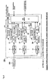
- FIG. 2 shows a diagram showing a structure of the device according to the present invention (a second embodiment).
- FIGs. 2 and 1 are different from each other in that receiving state counters 51, 52, ... 5N for counting receiving state signals (abnormal or normal) generated from the first check unit 21, the second check unit 22, ... the Nth check unit 2N respectively are provided, count signals S31, S32, ... S3N obtained from their counters are sent to a monitor setting unit for setting a priority to the data selector, and the priority in the data selector is reset based on the their count results.
- receiving state counters 51, 52, ... 5N for counting receiving state signals (abnormal or normal) generated from the first check unit 21, the second check unit 22, ... the Nth check unit 2N respectively are provided
- count signals S31, S32, ... S3N obtained from their counters are sent to a monitor setting unit for setting a priority to the data selector, and the priority in the data selector is reset based on the their count results.
- the received data compensating device 100 can be incorporated into various receiving apparatuses constituting the PLC system.
- FIG. 3 shows a diagram showing a structure of a master unit (or a slave unit) in which the device according to the present invention is incorporated.
- the received data compensating device 100 according to the present invention is incorporated in a master unit 6 or a slave unit 7.
- the master unit 6 or the slave unit 7 includes a receiving IC 200 constituting a physical layer, an IC 300 for a master unit or a slave unit which processes the received data obtained from the receiving IC 200, and a device 400 for controlling the IC 300.
- the device 400 has the function of selecting or setting a filter circuit such as an MPU, and the IC 300 for implementing the function of the master or the slave is controlled by the device 400.
- the received data compensating device 100 according to the present invention is incorporated in the input stage of the IC 300.
- the specific structure of the received data compensating device 100 which has been described with reference to FIGs. 1 and 2 can be used.
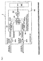
- FIG. 4 shows a diagram showing a structure of a repeater in which the device according to the present invention is incorporated.
- a repeater 8 has a high order side transmitting and receiving IC 201A and a low order side transmitting and receiving IC 201 B which function as physical layers, respectively.
- the ICs are connected to a high order side communication line and a low order side communication line.
- a device 500 can be constituted by an IC on which the technique according to the present invention such as ASIC is mounted, and the device 100 according to the present invention is incorporated in the device 500 corresponding to the input stage of the received data, respectively. More specifically, the device 100 according to the present invention is provided in the input stage of the received data acquired from the high order side transmitting/receiving IC, and furthermore, is provided in the input stage of the received data acquired from the low order side transmitting/receiving IC 201 B in the same manner. These two devices 100 according to the present invention are controlled by a transmitting and receiving control circuit 501, and the transmitting and receiving control circuit 501 is controlled by the MPU 100 through an MPU interface circuit 502. By employing such a structure, it is possible to enhance a redundancy for the received data to carry out an application to various communicating media or wiring configurations while implementing the function of the repeater
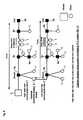
- FIG. 5 shows a diagram showing a wiring system constituting a PLC system (No. 1).
- reference numeral 6 denotes a master unit
- reference numeral 7 denotes a slave unit
- reference numeral 9a denotes a branch
- reference numeral 9b denotes a terminal resistor. Also in such a transmission line as to mix the various wiring configurations and transmitting media, it is possible to carry out an application without changing any specification irrespective of the transmitting media or the wiring configuration if the device 100 according to the present invention is incorporated in the master unit 6 and the slave unit 7, respectively.
- FIG. 6 shows a diagram showing a wiring system constituting the PLC system (No. 2).
- reference numeral 6 denotes a master unit
- reference numeral 7 denotes a slave unit
- reference numeral 8 denotes a repeater
- reference numeral 9a denotes a branch
- reference numeral 9b denotes a terminal resistor.
- a communicating system including various transmitting media and wiring configurations, it is possible to enhance a system adaptability by incorporating the device 100 according to the present invention in the repeater 8 in addition to the master unit 6 and the slave unit 7.
- FIG. 7 shows a view showing a more specific structure of a PLC system including a master unit and a slave unit.
- reference numeral 70 denotes a personal computer
- reference numeral 60 denotes a PLC
- reference numeral 6 denotes a master unit
- reference numeral 61 denotes a CPU unit
- reference numeral 7 denotes a slave unit
- reference numeral 8 denotes a repeater
- reference numeral 9b denotes a terminal resistor.
- the received data which are obtained from the receiving circuit constituting the physical layer are processed at the same time by a plurality of preprocessing units provided in parallel with each other on the output side and having the filtering function and the sampling function which have different characteristics from each other. Also in any quality of the transmission path and any wiring configuration, therefore, any processing system is adapted to the same characteristic. By one receiving processing device, therefore, it is possible to adapt transmission media and wiring configurations of various qualities. Thus, it is possible to enhance usability of the receiving device of this type.
Landscapes
- Engineering & Computer Science (AREA)
- Computer Networks & Wireless Communication (AREA)
- Signal Processing (AREA)
- Power Engineering (AREA)
- Communication Control (AREA)
- Dc Digital Transmission (AREA)
- Programmable Controllers (AREA)
Claims (7)
- Kompensiervorrichtung (100) für empfangene Daten, welche zwischen einer Empfängerschaltung (200) in einer Bitübertragungsschicht und einer Verarbeitungsvorrichtung, die die empfangenen Daten verwendet, vorgesehen ist, gekennzeichnet durch
eine Anzahl von Vorverarbeitungseinheiten (11, 12, ..., 1N), die parallel zueinander auf einer Ausgangsseite der Empfängerschaltung vorgesehen sind und jeweils eine Filterfunktion und eine Abtastfunktion mit für unterschiedliche Vorverarbeitungseinheiten unterschiedlicher Charakteristik aufweisen;
eine Anzahl von Prüfeinheiten (21, 22, ..., 2N), die jeweils in einer nächsten Stufe der Vorverarbeitungseinheit vorgesehen sind und dazu dienen, eine Zuverlässigkeitsprüfung der Daten gemäß einem Datenübertragungsblockformat eines Protokolls auszuführen;
eine Anzahl von Puffer-Einheiten (31, 32, ..., 3N), die jeweils im, einer nächsten Stufe der Prüfeinheit vorgesehen sind und dazu dienen, die von der Prüfeinheit verarbeiteten Daten zu speichern; und
einen Datenselektor (4) zur Überwachung einer Anzahl von Prüfergebnissen in den Prüfeinheiten und Auswählen und Ausgeben der Daten aus den Puffereinheiten, die ein OK-Prüfergebnis haben. - Kompensiervorrichtung nach Anspruch 1, wobei der Datenselektor (4) eines der Daten gemäß einer voreingestellten Priorität auswählt und ausgibt, wenn eine Anzahl von Daten der Puffereinheiten beruhend auf dem Prüfergebnis in der Prüfeinheit als OK festgestellt werden.
- Kompensiervorrichtung nach Anspruch 2, welche ferner eine Anzahl von Empfangsbedingungszahfern (51, 52, ..., 5N), jeder zur Zählung von OK und/oder NG des von den einzelnen Prüfeinheiten erhaltenen Prüfergebnisses, aufweist,
wobei der Datenselektor (4) die Priorität beruhend auf einer Tanzahl von Zählwerten der Empfangsbedingungszähler einstellt. - Kommunikationsmaster-Einheit einer programmierbaren Steuerung mit einer Kompensiervorrichtung (100) nach einem der vornstehenden Ansprüche für empfangene Daten in einer nächsten Stufe einer Empfängerschaltung (200) in einer Bitübertragungsschicht.
- Slave-Einheit einer programmierbaren Steuerung mit einer Kompensiervorrichtung (100) nach einem der Ansprüche 1 bis 3 für empfangene Daten in einer nächsten Stufe einer Empfängerschaltung in einer Bitübertragungsschicht.
- Repeater zur Verbindung mit einer oberseitigen Kommunikationsleitung und/oder einer unterseitigen Kommunikationsleitung mit einer Kompensiervorrichtung (100) nach einem der Ansprüche 1 bis 3 für empfangene Daten in einer nächsten Stufe einer Empfängerschaltung in einer Bitübertragungsschicht für jede Leitung.
- Repeater nach Anspruch 6, wobei der Repeater zwischen einer Kommunikationsmaster-Einheit und einer Slave-Einheit einer programmierbaren Steuerung vorgesehen ist.
Applications Claiming Priority (1)
| Application Number | Priority Date | Filing Date | Title |
|---|---|---|---|
| JP2005105543A JP4544420B2 (ja) | 2005-03-31 | 2005-03-31 | 受信データ補償装置 |
Publications (2)
| Publication Number | Publication Date |
|---|---|
| EP1710641A1 EP1710641A1 (de) | 2006-10-11 |
| EP1710641B1 true EP1710641B1 (de) | 2009-10-21 |
Family
ID=36602380
Family Applications (1)
| Application Number | Title | Priority Date | Filing Date |
|---|---|---|---|
| EP06005218A Ceased EP1710641B1 (de) | 2005-03-31 | 2006-03-14 | Kompensierungsvorrichtung für empfangene Daten |
Country Status (5)
| Country | Link |
|---|---|
| US (1) | US7546518B2 (de) |
| EP (1) | EP1710641B1 (de) |
| JP (1) | JP4544420B2 (de) |
| CN (1) | CN100539558C (de) |
| DE (1) | DE602006009865D1 (de) |
Families Citing this family (5)
| Publication number | Priority date | Publication date | Assignee | Title |
|---|---|---|---|---|
| JP2009049642A (ja) * | 2007-08-17 | 2009-03-05 | Omron Corp | 伝送システム |
| US20130219233A1 (en) * | 2012-02-21 | 2013-08-22 | Lsi Corporation | Systems and Methods for Quality Based Priority Data Processing |
| CN106982199B (zh) * | 2016-05-06 | 2020-04-14 | 深圳市永联科技股份有限公司 | 一种基于fpga和cpld的曼彻斯特码通讯协议自适应方法 |
| JP2018174369A (ja) * | 2017-03-31 | 2018-11-08 | 株式会社日立製作所 | 信号伝送方法及び通信システム |
| CN111448615B (zh) * | 2017-12-21 | 2024-07-30 | 雷迪奥米特医学公司 | 用于处理患者相关的医疗数据的系统和方法 |
Family Cites Families (13)
| Publication number | Priority date | Publication date | Assignee | Title |
|---|---|---|---|---|
| US3956589A (en) * | 1973-11-26 | 1976-05-11 | Paradyne Corporation | Data telecommunication system |
| JPH03155228A (ja) | 1989-11-14 | 1991-07-03 | Toshiba Corp | ダイバーシティ受信装置 |
| JP3211034B2 (ja) * | 1991-10-31 | 2001-09-25 | オムロン株式会社 | ディジタル信号のノイズ成分除去装置 |
| JPH07327255A (ja) * | 1994-06-01 | 1995-12-12 | Matsushita Graphic Commun Syst Inc | 通信装置 |
| JPH0823281A (ja) * | 1994-07-07 | 1996-01-23 | Oki Electric Ind Co Ltd | 誤り検出訂正装置 |
| JPH10173723A (ja) * | 1996-12-12 | 1998-06-26 | Fujitsu Ltd | データ転送方法及びデータ転送装置 |
| US5961658A (en) * | 1997-05-23 | 1999-10-05 | Cirrus Logic, Inc. | PR4 equalization and an EPR4 remod/demod sequence detector in a sampled amplitude read channel |
| US6519715B1 (en) * | 1998-05-22 | 2003-02-11 | Hitachi, Ltd. | Signal processing apparatus and a data recording and reproducing apparatus including local memory processor |
| JP2000236357A (ja) * | 1999-02-16 | 2000-08-29 | Canon Inc | 情報処理装置およびその処理方法 |
| JP4198904B2 (ja) * | 2001-06-11 | 2008-12-17 | 富士通株式会社 | 記録再生装置、信号復号回路、エラー訂正方法、及び反復型復号器 |
| US6889154B2 (en) * | 2002-04-18 | 2005-05-03 | Infineon Technologies Ag | Method and apparatus for calibrating data-dependent noise prediction |
| JP4125109B2 (ja) * | 2002-12-12 | 2008-07-30 | 富士通株式会社 | インターフェース装置,sonet多重分離装置,伝送システムおよびフレーム伝送方法 |
| JP4019946B2 (ja) * | 2003-01-14 | 2007-12-12 | オムロン株式会社 | ネットワークシステムのモニタ方法及びモニタリングシステム並びにリピータ及びモニタ装置 |
-
2005
- 2005-03-31 JP JP2005105543A patent/JP4544420B2/ja not_active Expired - Lifetime
-
2006
- 2006-03-13 CN CNB2006100678570A patent/CN100539558C/zh not_active Expired - Fee Related
- 2006-03-14 US US11/374,432 patent/US7546518B2/en active Active
- 2006-03-14 DE DE602006009865T patent/DE602006009865D1/de not_active Expired - Lifetime
- 2006-03-14 EP EP06005218A patent/EP1710641B1/de not_active Ceased
Also Published As
| Publication number | Publication date |
|---|---|
| DE602006009865D1 (de) | 2009-12-03 |
| JP2006287665A (ja) | 2006-10-19 |
| EP1710641A1 (de) | 2006-10-11 |
| US20060242472A1 (en) | 2006-10-26 |
| CN1842069A (zh) | 2006-10-04 |
| JP4544420B2 (ja) | 2010-09-15 |
| US7546518B2 (en) | 2009-06-09 |
| CN100539558C (zh) | 2009-09-09 |
Similar Documents
| Publication | Publication Date | Title |
|---|---|---|
| EP1533708A2 (de) | Signalübertragungsvorrichtung und -verfahren | |
| EP1529373B1 (de) | Netzwerküberwachungsgerät und -verfahren | |
| KR102518285B1 (ko) | PCIe 인터페이스 및 인터페이스 시스템 | |
| US20090323547A1 (en) | System and method for packet based communications and arrangement therefor | |
| JPH0783382B2 (ja) | 高速の直列デ−タパタ−ン入力信号を並列デ−タパタ−ン出力に変換するための方法 | |
| EP1710641B1 (de) | Kompensierungsvorrichtung für empfangene Daten | |
| EP0923035A2 (de) | Kodierschaltung und Verfahren zum Erkennen von Blokcodegrenzen und Herstellen der Synchronization zwischen Verwürfler und Entwürfler | |
| CN112291128B (zh) | 基于总线的通信系统、片上系统和用于其的方法 | |
| US6356584B1 (en) | Method for the clocked serial data transmission of data blocks of identical block length | |
| CN115694740B (zh) | Uvm验证平台系统和验证方法 | |
| US7184395B2 (en) | Providing reconditioned signals at a plurality of ports | |
| JP3997106B2 (ja) | データ伝送速度調停方法および光通信装置 | |
| US7840624B2 (en) | Digital low pass filter | |
| US6769039B2 (en) | Data processing apparatus with circuit for confirming normality of serial transmission data | |
| US7290163B2 (en) | Method and circuit for deciding data transfer rate | |
| EP1785886A1 (de) | Elektronisches Gerät und Datenübertragungssteuerungsverfahren | |
| US7266624B1 (en) | Programmable layered sub-system interface | |
| JP3778976B2 (ja) | デジタルミキシング装置のインサーション回路 | |
| JP3581112B2 (ja) | データ送信方法および送信回路並びに通信機器 | |
| CN102545948B (zh) | 建立网络连接的方法与相关的通信装置 | |
| KR0160502B1 (ko) | 통신 포트의 구조 검출 장치 | |
| WO2006088566A2 (en) | Hdsl optical fiber transmission system and method | |
| JP2616695B2 (ja) | 回線切替装置 | |
| JP3708105B2 (ja) | データ伝送装置およびデータ伝送システム | |
| CN117595892A (zh) | 收发装置及双向通信系统 |
Legal Events
| Date | Code | Title | Description |
|---|---|---|---|
| PUAI | Public reference made under article 153(3) epc to a published international application that has entered the european phase |
Free format text: ORIGINAL CODE: 0009012 |
|
| AK | Designated contracting states |
Kind code of ref document: A1 Designated state(s): AT BE BG CH CY CZ DE DK EE ES FI FR GB GR HU IE IS IT LI LT LU LV MC NL PL PT RO SE SI SK TR |
|
| AX | Request for extension of the european patent |
Extension state: AL BA HR MK YU |
|
| 17P | Request for examination filed |
Effective date: 20070411 |
|
| 17Q | First examination report despatched |
Effective date: 20070521 |
|
| AKX | Designation fees paid |
Designated state(s): DE FR GB IT |
|
| GRAP | Despatch of communication of intention to grant a patent |
Free format text: ORIGINAL CODE: EPIDOSNIGR1 |
|
| GRAS | Grant fee paid |
Free format text: ORIGINAL CODE: EPIDOSNIGR3 |
|
| GRAA | (expected) grant |
Free format text: ORIGINAL CODE: 0009210 |
|
| AK | Designated contracting states |
Kind code of ref document: B1 Designated state(s): DE FR GB IT |
|
| REG | Reference to a national code |
Ref country code: GB Ref legal event code: FG4D |
|
| REF | Corresponds to: |
Ref document number: 602006009865 Country of ref document: DE Date of ref document: 20091203 Kind code of ref document: P |
|
| PLBE | No opposition filed within time limit |
Free format text: ORIGINAL CODE: 0009261 |
|
| STAA | Information on the status of an ep patent application or granted ep patent |
Free format text: STATUS: NO OPPOSITION FILED WITHIN TIME LIMIT |
|
| 26N | No opposition filed |
Effective date: 20100722 |
|
| REG | Reference to a national code |
Ref country code: DE Ref legal event code: R082 Ref document number: 602006009865 Country of ref document: DE Representative=s name: KILIAN KILIAN & PARTNER, DE Ref country code: DE Ref legal event code: R082 Ref document number: 602006009865 Country of ref document: DE Representative=s name: KILIAN KILIAN & PARTNER MBB PATENTANWAELTE, DE |
|
| REG | Reference to a national code |
Ref country code: FR Ref legal event code: PLFP Year of fee payment: 11 |
|
| REG | Reference to a national code |
Ref country code: FR Ref legal event code: PLFP Year of fee payment: 12 |
|
| REG | Reference to a national code |
Ref country code: FR Ref legal event code: PLFP Year of fee payment: 13 |
|
| PGFP | Annual fee paid to national office [announced via postgrant information from national office to epo] |
Ref country code: IT Payment date: 20190326 Year of fee payment: 14 |
|
| GBPC | Gb: european patent ceased through non-payment of renewal fee |
Effective date: 20200314 |
|
| PG25 | Lapsed in a contracting state [announced via postgrant information from national office to epo] |
Ref country code: GB Free format text: LAPSE BECAUSE OF NON-PAYMENT OF DUE FEES Effective date: 20200314 |
|
| PG25 | Lapsed in a contracting state [announced via postgrant information from national office to epo] |
Ref country code: IT Free format text: LAPSE BECAUSE OF NON-PAYMENT OF DUE FEES Effective date: 20200314 |
|
| PGFP | Annual fee paid to national office [announced via postgrant information from national office to epo] |
Ref country code: FR Payment date: 20230208 Year of fee payment: 18 |
|
| PGFP | Annual fee paid to national office [announced via postgrant information from national office to epo] |
Ref country code: DE Payment date: 20230131 Year of fee payment: 18 |
|
| REG | Reference to a national code |
Ref country code: DE Ref legal event code: R119 Ref document number: 602006009865 Country of ref document: DE |
|
| PG25 | Lapsed in a contracting state [announced via postgrant information from national office to epo] |
Ref country code: DE Free format text: LAPSE BECAUSE OF NON-PAYMENT OF DUE FEES Effective date: 20241001 |
|
| PG25 | Lapsed in a contracting state [announced via postgrant information from national office to epo] |
Ref country code: FR Free format text: LAPSE BECAUSE OF NON-PAYMENT OF DUE FEES Effective date: 20240331 |
|
| PG25 | Lapsed in a contracting state [announced via postgrant information from national office to epo] |
Ref country code: FR Free format text: LAPSE BECAUSE OF NON-PAYMENT OF DUE FEES Effective date: 20240331 Ref country code: DE Free format text: LAPSE BECAUSE OF NON-PAYMENT OF DUE FEES Effective date: 20241001 |