EP1702352B1 - Base de fabrication de nanotube - Google Patents
Base de fabrication de nanotube Download PDFInfo
- Publication number
- EP1702352B1 EP1702352B1 EP04821227A EP04821227A EP1702352B1 EP 1702352 B1 EP1702352 B1 EP 1702352B1 EP 04821227 A EP04821227 A EP 04821227A EP 04821227 A EP04821227 A EP 04821227A EP 1702352 B1 EP1702352 B1 EP 1702352B1
- Authority
- EP
- European Patent Office
- Prior art keywords
- layer
- hfn
- catalyst
- substrate
- island
- Prior art date
- Legal status (The legal status is an assumption and is not a legal conclusion. Google has not performed a legal analysis and makes no representation as to the accuracy of the status listed.)
- Expired - Lifetime
Links
- 239000002071 nanotube Substances 0.000 title claims abstract description 24
- 238000004519 manufacturing process Methods 0.000 title claims description 6
- 239000003054 catalyst Substances 0.000 claims abstract description 27
- 239000000758 substrate Substances 0.000 claims abstract description 18
- OKTJSMMVPCPJKN-UHFFFAOYSA-N Carbon Chemical compound [C] OKTJSMMVPCPJKN-UHFFFAOYSA-N 0.000 claims abstract description 11
- XEEYBQQBJWHFJM-UHFFFAOYSA-N Iron Chemical compound [Fe] XEEYBQQBJWHFJM-UHFFFAOYSA-N 0.000 claims abstract description 10
- 238000000034 method Methods 0.000 claims abstract description 10
- PXHVJJICTQNCMI-UHFFFAOYSA-N Nickel Chemical compound [Ni] PXHVJJICTQNCMI-UHFFFAOYSA-N 0.000 claims abstract description 9
- 230000005684 electric field Effects 0.000 claims abstract description 5
- 229910052759 nickel Inorganic materials 0.000 claims abstract description 5
- 229910052742 iron Inorganic materials 0.000 claims abstract description 4
- 229910052799 carbon Inorganic materials 0.000 claims abstract description 3
- 239000000463 material Substances 0.000 claims description 25
- 238000000137 annealing Methods 0.000 claims description 12
- 238000002161 passivation Methods 0.000 claims description 10
- XUIMIQQOPSSXEZ-UHFFFAOYSA-N Silicon Chemical compound [Si] XUIMIQQOPSSXEZ-UHFFFAOYSA-N 0.000 claims description 7
- 238000000151 deposition Methods 0.000 claims description 7
- 229910052710 silicon Inorganic materials 0.000 claims description 7
- 239000010703 silicon Substances 0.000 claims description 7
- 238000000059 patterning Methods 0.000 claims description 3
- ZOKXTWBITQBERF-UHFFFAOYSA-N Molybdenum Chemical compound [Mo] ZOKXTWBITQBERF-UHFFFAOYSA-N 0.000 claims description 2
- KJTLSVCANCCWHF-UHFFFAOYSA-N Ruthenium Chemical compound [Ru] KJTLSVCANCCWHF-UHFFFAOYSA-N 0.000 claims description 2
- HCHKCACWOHOZIP-UHFFFAOYSA-N Zinc Chemical compound [Zn] HCHKCACWOHOZIP-UHFFFAOYSA-N 0.000 claims description 2
- 229910017052 cobalt Inorganic materials 0.000 claims description 2
- 239000010941 cobalt Substances 0.000 claims description 2
- GUTLYIVDDKVIGB-UHFFFAOYSA-N cobalt atom Chemical compound [Co] GUTLYIVDDKVIGB-UHFFFAOYSA-N 0.000 claims description 2
- 229910052750 molybdenum Inorganic materials 0.000 claims description 2
- 239000011733 molybdenum Substances 0.000 claims description 2
- 229910052707 ruthenium Inorganic materials 0.000 claims description 2
- 229910052725 zinc Inorganic materials 0.000 claims description 2
- 239000011701 zinc Substances 0.000 claims description 2
- 239000010410 layer Substances 0.000 claims 26
- 238000005520 cutting process Methods 0.000 claims 1
- 239000011241 protective layer Substances 0.000 claims 1
- 229910052751 metal Inorganic materials 0.000 abstract description 34
- 239000002184 metal Substances 0.000 abstract description 34
- 239000007789 gas Substances 0.000 abstract description 9
- IJGRMHOSHXDMSA-UHFFFAOYSA-N Atomic nitrogen Chemical compound N#N IJGRMHOSHXDMSA-UHFFFAOYSA-N 0.000 abstract description 5
- 229910052735 hafnium Inorganic materials 0.000 abstract description 2
- VBJZVLUMGGDVMO-UHFFFAOYSA-N hafnium atom Chemical compound [Hf] VBJZVLUMGGDVMO-UHFFFAOYSA-N 0.000 abstract description 2
- 229910052757 nitrogen Inorganic materials 0.000 abstract description 2
- 239000004020 conductor Substances 0.000 description 9
- 150000002739 metals Chemical class 0.000 description 9
- 239000002041 carbon nanotube Substances 0.000 description 8
- VYPSYNLAJGMNEJ-UHFFFAOYSA-N Silicium dioxide Chemical compound O=[Si]=O VYPSYNLAJGMNEJ-UHFFFAOYSA-N 0.000 description 7
- 229910021393 carbon nanotube Inorganic materials 0.000 description 7
- 230000003197 catalytic effect Effects 0.000 description 6
- VNWKTOKETHGBQD-UHFFFAOYSA-N methane Chemical compound C VNWKTOKETHGBQD-UHFFFAOYSA-N 0.000 description 6
- 230000015572 biosynthetic process Effects 0.000 description 5
- -1 aluminum (Al) Chemical class 0.000 description 4
- 230000008021 deposition Effects 0.000 description 4
- 239000002109 single walled nanotube Substances 0.000 description 4
- 239000000956 alloy Substances 0.000 description 3
- 229910045601 alloy Inorganic materials 0.000 description 3
- 238000011161 development Methods 0.000 description 3
- 239000000377 silicon dioxide Substances 0.000 description 3
- 229910052581 Si3N4 Inorganic materials 0.000 description 2
- 229910052681 coesite Inorganic materials 0.000 description 2
- 229910052906 cristobalite Inorganic materials 0.000 description 2
- 239000000203 mixture Substances 0.000 description 2
- HQVNEWCFYHHQES-UHFFFAOYSA-N silicon nitride Chemical compound N12[Si]34N5[Si]62N3[Si]51N64 HQVNEWCFYHHQES-UHFFFAOYSA-N 0.000 description 2
- 229910052682 stishovite Inorganic materials 0.000 description 2
- 229910052905 tridymite Inorganic materials 0.000 description 2
- UFHFLCQGNIYNRP-UHFFFAOYSA-N Hydrogen Chemical compound [H][H] UFHFLCQGNIYNRP-UHFFFAOYSA-N 0.000 description 1
- 229910005883 NiSi Inorganic materials 0.000 description 1
- ATJFFYVFTNAWJD-UHFFFAOYSA-N Tin Chemical compound [Sn] ATJFFYVFTNAWJD-UHFFFAOYSA-N 0.000 description 1
- 229910052782 aluminium Inorganic materials 0.000 description 1
- XAGFODPZIPBFFR-UHFFFAOYSA-N aluminium Chemical compound [Al] XAGFODPZIPBFFR-UHFFFAOYSA-N 0.000 description 1
- PNEYBMLMFCGWSK-UHFFFAOYSA-N aluminium oxide Inorganic materials [O-2].[O-2].[O-2].[Al+3].[Al+3] PNEYBMLMFCGWSK-UHFFFAOYSA-N 0.000 description 1
- QVGXLLKOCUKJST-UHFFFAOYSA-N atomic oxygen Chemical compound [O] QVGXLLKOCUKJST-UHFFFAOYSA-N 0.000 description 1
- 230000004888 barrier function Effects 0.000 description 1
- 238000009792 diffusion process Methods 0.000 description 1
- 229910002804 graphite Inorganic materials 0.000 description 1
- 239000010439 graphite Substances 0.000 description 1
- 239000001257 hydrogen Substances 0.000 description 1
- 229910052739 hydrogen Inorganic materials 0.000 description 1
- 238000005259 measurement Methods 0.000 description 1
- 239000002923 metal particle Substances 0.000 description 1
- 238000003801 milling Methods 0.000 description 1
- 238000012986 modification Methods 0.000 description 1
- 230000004048 modification Effects 0.000 description 1
- 239000002048 multi walled nanotube Substances 0.000 description 1
- 239000002105 nanoparticle Substances 0.000 description 1
- 239000001301 oxygen Substances 0.000 description 1
- 229910052760 oxygen Inorganic materials 0.000 description 1
- 238000012545 processing Methods 0.000 description 1
- 239000010453 quartz Substances 0.000 description 1
- 229910052594 sapphire Inorganic materials 0.000 description 1
- 239000010980 sapphire Substances 0.000 description 1
- 238000004544 sputter deposition Methods 0.000 description 1
- 230000002194 synthesizing effect Effects 0.000 description 1
- 238000002230 thermal chemical vapour deposition Methods 0.000 description 1
- 229910052723 transition metal Inorganic materials 0.000 description 1
- 210000005239 tubule Anatomy 0.000 description 1
Images


Classifications
-
- C—CHEMISTRY; METALLURGY
- C30—CRYSTAL GROWTH
- C30B—SINGLE-CRYSTAL GROWTH; UNIDIRECTIONAL SOLIDIFICATION OF EUTECTIC MATERIAL OR UNIDIRECTIONAL DEMIXING OF EUTECTOID MATERIAL; REFINING BY ZONE-MELTING OF MATERIAL; PRODUCTION OF A HOMOGENEOUS POLYCRYSTALLINE MATERIAL WITH DEFINED STRUCTURE; SINGLE CRYSTALS OR HOMOGENEOUS POLYCRYSTALLINE MATERIAL WITH DEFINED STRUCTURE; AFTER-TREATMENT OF SINGLE CRYSTALS OR A HOMOGENEOUS POLYCRYSTALLINE MATERIAL WITH DEFINED STRUCTURE; APPARATUS THEREFOR
- C30B29/00—Single crystals or homogeneous polycrystalline material with defined structure characterised by the material or by their shape
- C30B29/60—Single crystals or homogeneous polycrystalline material with defined structure characterised by the material or by their shape characterised by shape
- C30B29/605—Products containing multiple oriented crystallites, e.g. columnar crystallites
-
- B—PERFORMING OPERATIONS; TRANSPORTING
- B82—NANOTECHNOLOGY
- B82Y—SPECIFIC USES OR APPLICATIONS OF NANOSTRUCTURES; MEASUREMENT OR ANALYSIS OF NANOSTRUCTURES; MANUFACTURE OR TREATMENT OF NANOSTRUCTURES
- B82Y30/00—Nanotechnology for materials or surface science, e.g. nanocomposites
-
- B—PERFORMING OPERATIONS; TRANSPORTING
- B82—NANOTECHNOLOGY
- B82Y—SPECIFIC USES OR APPLICATIONS OF NANOSTRUCTURES; MEASUREMENT OR ANALYSIS OF NANOSTRUCTURES; MANUFACTURE OR TREATMENT OF NANOSTRUCTURES
- B82Y40/00—Manufacture or treatment of nanostructures
-
- C—CHEMISTRY; METALLURGY
- C01—INORGANIC CHEMISTRY
- C01B—NON-METALLIC ELEMENTS; COMPOUNDS THEREOF; METALLOIDS OR COMPOUNDS THEREOF NOT COVERED BY SUBCLASS C01C
- C01B32/00—Carbon; Compounds thereof
- C01B32/15—Nano-sized carbon materials
- C01B32/158—Carbon nanotubes
- C01B32/16—Preparation
- C01B32/162—Preparation characterised by catalysts
-
- Y—GENERAL TAGGING OF NEW TECHNOLOGICAL DEVELOPMENTS; GENERAL TAGGING OF CROSS-SECTIONAL TECHNOLOGIES SPANNING OVER SEVERAL SECTIONS OF THE IPC; TECHNICAL SUBJECTS COVERED BY FORMER USPC CROSS-REFERENCE ART COLLECTIONS [XRACs] AND DIGESTS
- Y10—TECHNICAL SUBJECTS COVERED BY FORMER USPC
- Y10S—TECHNICAL SUBJECTS COVERED BY FORMER USPC CROSS-REFERENCE ART COLLECTIONS [XRACs] AND DIGESTS
- Y10S977/00—Nanotechnology
- Y10S977/70—Nanostructure
- Y10S977/734—Fullerenes, i.e. graphene-based structures, such as nanohorns, nanococoons, nanoscrolls or fullerene-like structures, e.g. WS2 or MoS2 chalcogenide nanotubes, planar C3N4, etc.
- Y10S977/742—Carbon nanotubes, CNTs
-
- Y—GENERAL TAGGING OF NEW TECHNOLOGICAL DEVELOPMENTS; GENERAL TAGGING OF CROSS-SECTIONAL TECHNOLOGIES SPANNING OVER SEVERAL SECTIONS OF THE IPC; TECHNICAL SUBJECTS COVERED BY FORMER USPC CROSS-REFERENCE ART COLLECTIONS [XRACs] AND DIGESTS
- Y10—TECHNICAL SUBJECTS COVERED BY FORMER USPC
- Y10T—TECHNICAL SUBJECTS COVERED BY FORMER US CLASSIFICATION
- Y10T428/00—Stock material or miscellaneous articles
- Y10T428/30—Self-sustaining carbon mass or layer with impregnant or other layer
Definitions
- the present invention relates to a deposition of material and particularly to high temperature deposition of metal on a wafer. More preferably it relates to such deposition for the fabrication of nanotubes.
- Carbon nanotubes are a recent technological development. They may be hollow graphite tubules. In an isolated form, individual nanotubes may be useful to making microscopic electrical, mechanical and electromechanical devices. Single-walled nanotubes (SWNTs) are desirable. However, obtaining high quality, single-walled nanotubes has been generally a difficult task. Existing methods for the production of nanotubes often yield bundled forms of tangled and often multi-walled nanotubes. Such tangled nanotubes are very difficult to isolate into discrete elements for use in the fabrication of various electronic and/or devices.
- SWNTs Single-walled nanotubes
- EP 1,061,043 discloses a low temperature method of synthesizing carbon nanotubes in which a metal catalyst layer is formed over a substrate.
- the metal catalyst layer is etched to form isolated nano-sized catalytic metal particles from which are grown vertically aligned carbon nanotubes through thermal chemical vapour deposition.
- FR 2832995 describes a method for the catalytic growth of nanotubes on a substrate which comprises forming a diffusion barrier film of an NiSi alloy at the surface of a growth substrate.
- US 2002/0024099 describes a method of making a nanotube transistor on a silicon substrate.
- Nano islands are typically formed by annealing a thin catalytic metal to a high temperature (i.e., 900 to 1000 degrees C). Typically the formation of nanotubes by a high temperature anneal, leaves conductive islands but no macroscopic conductive path to permit external electrical contact to the nanotube.
- a metal typically forms an alloy with the catalytic metal preventing the formation of islands.
- a metal can be applied to the nanotubes after growth but this process involves both pre- and post- CNT growth processing.
- the present invention solves these problems by the method according to claim 1 and meets those objectives.
- Metal islands having a particular material formed with an appropriate conducting metal have been developed to support the successful growth of nanotubes on a resulting structure as set forth in claims 5, 8, and 9 for a reliable electrical connection to the nanotubes.
- a metal capable of withstanding deposition temperatures around 900 degrees Centigrade (C) that may be incorporated in metal islands for the growth of carbon nanotubes is one aspect of the present invention.
- C degrees Centigrade
- the islands may be formed by exposing a thin metal such an iron (Fe) to high temperatures in an inert environment. At these high temperatures, the thin metal may ball up to form islands of a diameter on the order of the thickness. Small islands may yield single wall small diameter nanotubes. To make contact to these islands may require a patternable conducting metal.
- a solution may be taking hafnium (Hf) metal, depositing it, and annealing it in nitrogen (N 2 ).
- the result may be HfN.
- This material may be conductive and support the formation of Fe and nickel (Ni) islands with a 900 degree C inert anneal.
- Other catalyst metals may include, but are not limited to, molybdenum, cobalt, ruthenium, zinc and oxides of the metals.
- the catalyst materials may also include various alloys or mixtures of these metals including Fe and Ni, such as Mo-Fe. Carbon nanotubes may be formed on these structures. Briefly in sum, the Hf metal may be deposited and annealed in N 2 after patterning.
- HfN metal conductor lead material may be Hf x N 1-x metal having a resistance between 10ohms/sq and 10Kohm/ square.
- the present HfN is not a typical stoichiometric HfN. However, the HfN may be stoichiometric or non-stoichiometric.
- Other lead material may include, but are not limited to, Hf, transition metal nitrides, including ZrN, TaN, TiN, HfN, other conductive metals, Hf, conductive metals and oxides of the metals.
- the material may be ITO or some other conductive oxide.
- Si wafer 11 For an illustrative embodiment, one may start with silicon (Si) wafer 11, as in Figure 1 .
- Other wafer or other substrate materials that may be selected include, but are not limited to, silica, quartz, silicon nitride, sapphire and alumina.
- a thermal oxide (SiO 2 ) 12 may be grown on wafer 11, as indicated in Figure 2 .
- Substrate 11 may be substituted for layer 12.
- Oxide 12 may have a thickness of about or greater than 1000 angstroms.
- another insulative or semi-insulative material may be used as a layer 12.
- a layer of Hf material 13 may be deposited on SiO 2 layer 12.
- the thickness of the layer of Hf material 13 may be between 500 and 1000 angstroms. Then the Hf material 13 may be annealed in an N 2 environment for about two hours at a temperature of 400 to 450 degrees C. However, the time duration may be longer or shorter and the temperature may be as low as 300 degrees C or it may be greater than 450 degrees C. Also, another gas may be used for annealing. This should result in a layer 14 of HfN, as in Figure 4 . HfN layer 14 may be patterned as conductor strips 15 for external connections. Cross-sectional and plan views are shown in Figures 5a and 5b , respectively.
- the resultant exposed materials may be passivated with a layer 16, for example, silicon nitride or the like, such as other passivation materials.
- Passivation layer 16 is shown in the cross-sectional and plan views of Figures 6a and 6b .
- vias 17 may be etched or cut through passivation layer 16 to HfN strips 15, for external conductor 25 connections.
- vias 18 may be etched or cut through passivation layer 16 to HfN conducting strips 15 for connection to catalyst islands 21 of Figure 9 .
- Vias 17 and 18, shown in figures 7a and 7b may be made with for example a plasma etch.
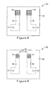
- a thin catalyst layer 19, such as Ni or Fe may be deposited on and in vias 18 to an exposed portion of HfN strip 15 at room temperature, such as with sputtering. Other appropriate materials may instead be deposited. That layer 19 of catalyst material may be between 50 and 100 angstroms thick. Then, the catalyst may be patterned with liftoff or by milling to result in catalyst portions 19, as indicated in Figure 8 . Afterwards, the patterned catalyst deposited layer 19 may be annealed in a forming gas composed of about 15 percent of hydrogen and 85 percent of nitrogen, for about 30 minutes at about 900 degrees C. However, various gases and mixtures at a temperature with a range between 500 and 1200 degrees for a period ranging between 15 minutes and two hours may suffice for annealing. This annealing may form an island 21 of each catalyst material portion 19, as illustrated in Figure 9 . Also, during the annealing, structure 20 may be purged of gases such as oxygen.
- the gas may be switched to methane (at a rate of 1700 or 850 sccm) and H 2 (at a rate of 1700 or 850 sccm) for a growing of a carbon nanotube.
- methane at a rate of 1700 or 850 sccm
- H 2 at a rate of 1700 or 850 sccm
- Other carbon-containing gases may be used in lieu of methane.
- sccm means standard cubic centimeters per minute.
- Standard means that the measurement is referenced to zero degrees C at 760 Torr, i.e., 1 atm pressure.
- Methane may be also mixed in with the forming gas at a ratio of one to one at about 1000 sccm. The flow rates may be other than stated here for satisfactory annealing and growing nanotubes.
- An electric field of about one volt per micron of gap 22 may be applied during the growing of the nanotubes. For instance, a bridging of a 10 micron gap with a growing nanotube would use a 10 volt electric field. Other electric field intensities may be incorporated.
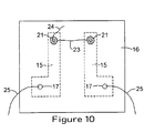
- a nanotube 23 may be grown connecting two islands 21, as illustrated in Figure 10 .
- an unconnected nanotube 24 may be grown for one purpose or another.
- Conductors 25 may be bonded, soldered, or attached in some fashion to HFN conducting strips 15, respectively.
Landscapes
- Chemical & Material Sciences (AREA)
- Engineering & Computer Science (AREA)
- Nanotechnology (AREA)
- Materials Engineering (AREA)
- Crystallography & Structural Chemistry (AREA)
- Organic Chemistry (AREA)
- General Physics & Mathematics (AREA)
- Physics & Mathematics (AREA)
- Condensed Matter Physics & Semiconductors (AREA)
- Metallurgy (AREA)
- Composite Materials (AREA)
- Manufacturing & Machinery (AREA)
- Chemical Kinetics & Catalysis (AREA)
- Inorganic Chemistry (AREA)
- Carbon And Carbon Compounds (AREA)
- Catalysts (AREA)
Abstract
Claims (10)
- Procédé de fabrication d'une structure pour la croissance de nanotubes, comprenant :la croissance d'un oxyde thermique (12) sur une surface d'une tranche de silicium (11) ;le dépôt d'une couche de Hf (13) sur l'oxyde thermique ;le recuit de la couche de Hf dans du N2 pour obtenir une couche de HfN (14) ;la gravure (15) de la couche de HfN ;la formation d'une couche de passivation (16) sur la couche de HfN ;la découpe de trous d'interconnexion (18) à travers la couche de passivation jusqu'à la couche de HfN ;le dépôt d'un matériau catalyseur (19) dans les trous d'interconnexion ;la gravure du matériau catalyseur ; etle recuit du matériau catalyseur pour former des îlots catalyseurs (21).
- Procédé selon la revendication 1, dans lequel :la couche de Hf (13) est recuite dans du N2 pendant plus d'une heure à une température supérieure à 300 degrés Celsius ; etle matériau catalyseur (19) est recuit dans un gaz de formation.
- Procédé selon la revendication 2, dans lequel le matériau catalyseur (19) est recuit à une température supérieure à 700 degrés Celsius pendant un temps supérieur à quinze minutes.
- Procédé selon la revendication 3, dans lequel le gaz de formation comprend du H2 et du N2.
- Structure comprenant :un substrat (11) ;une couche d'oxyde (12) sur le substrat ;une couche de HfN (15) sur la couche d'oxyde ;une couche de passivation (16) sur la couche de HfN, comportant au moins un trou d'interconnexion (18) à travers la couche de passivation jusqu'au HfN ; etun îlot catalyseur (21) formé sur le(s) trou(s) d'interconnexion relié à la couche de HfN ; etdans laquelle le substrat (11) est une tranche de silicium.
- Structure selon la revendication 5, dans laquelle l'îlot catalyseur (21) est placé dans un environnement comportant un gaz contenant du carbone, une température supérieure à 500 degrés Celsius et un champ électrique.
- Structure selon la revendication 6, dans laquelle l'environnement est maintenu jusqu'à la croissance d'un nanotube souhaité (23, 24).
- Structure comprenant :un substrat (11) ;une couche isolante (12) sur le substrat ;une couche de HfN (15) sur la couche isolante ;une couche protectrice (16) sur la couche de HfN ; etau moins un îlot catalyseur (21) en contact avec la couche de HfN.
- Structure pour la croissance d'un nanotube, comprenant :un substrat de silicium (11) ;une couche au moins partiellement isolante (12) sur une surface du substrat de silicium ;une couche (15) de HfN sur la surface du substrat de silicium ;une couche de passivation (16) sur une surface de la couche (15) de HfN ; etun moyen pour former au moins un îlot catalyseur (21) faisant contact avec la couche de HfN.
- Structure selon la revendication 9, dans laquelle cet/ces îlot(s) catalyseur(s) (21) comprend/comprennent un matériau choisi dans un groupe constitué par le fer, le nickel, le zinc, le molybdène, le cobalt, le ruthénium et les oxydes de ceux-ci.
Applications Claiming Priority (2)
| Application Number | Priority Date | Filing Date | Title |
|---|---|---|---|
| US10/749,637 US7276285B2 (en) | 2003-12-31 | 2003-12-31 | Nanotube fabrication basis |
| PCT/US2004/042270 WO2005071715A2 (fr) | 2003-12-31 | 2004-12-15 | Base de fabrication de nanotube |
Publications (2)
| Publication Number | Publication Date |
|---|---|
| EP1702352A2 EP1702352A2 (fr) | 2006-09-20 |
| EP1702352B1 true EP1702352B1 (fr) | 2009-07-08 |
Family
ID=34711107
Family Applications (1)
| Application Number | Title | Priority Date | Filing Date |
|---|---|---|---|
| EP04821227A Expired - Lifetime EP1702352B1 (fr) | 2003-12-31 | 2004-12-15 | Base de fabrication de nanotube |
Country Status (4)
| Country | Link |
|---|---|
| US (1) | US7276285B2 (fr) |
| EP (1) | EP1702352B1 (fr) |
| DE (1) | DE602004021962D1 (fr) |
| WO (1) | WO2005071715A2 (fr) |
Families Citing this family (4)
| Publication number | Priority date | Publication date | Assignee | Title |
|---|---|---|---|---|
| KR100667652B1 (ko) * | 2005-09-06 | 2007-01-12 | 삼성전자주식회사 | 탄소나노튜브를 이용한 배선 형성 방법 |
| WO2010031052A2 (fr) * | 2008-09-15 | 2010-03-18 | Bp Corporation North America Inc. | Procédé de détermination de conditions dans un trou de sonde à partir de données de mesures réparties |
| US20100127459A1 (en) * | 2008-11-25 | 2010-05-27 | Honeywell International Inc. | Metal-to-metal seal utilizing a flanged pinch-off tube and related apparatus and method |
| TWI479547B (zh) * | 2011-05-04 | 2015-04-01 | Univ Nat Cheng Kung | 薄膜電晶體之製備方法及頂閘極式薄膜電晶體 |
Family Cites Families (16)
| Publication number | Priority date | Publication date | Assignee | Title |
|---|---|---|---|---|
| JPH03157965A (ja) * | 1989-11-15 | 1991-07-05 | Nec Corp | 半導体装置 |
| JPH07118270B2 (ja) * | 1993-10-25 | 1995-12-18 | 日本電気株式会社 | カーボンナノチューブトランジスタ |
| US5710656A (en) * | 1996-07-30 | 1998-01-20 | Lucent Technologies Inc. | Micromechanical optical modulator having a reduced-mass composite membrane |
| US6143474A (en) * | 1998-05-07 | 2000-11-07 | Taiwan Semiconductor Manufacturing Company | Method of fabricating polysilicon structures with different resistance values for gate electrodes, resistors, and capacitor plates |
| US6346189B1 (en) | 1998-08-14 | 2002-02-12 | The Board Of Trustees Of The Leland Stanford Junior University | Carbon nanotube structures made using catalyst islands |
| KR100376197B1 (ko) | 1999-06-15 | 2003-03-15 | 일진나노텍 주식회사 | 탄소 소오스 가스 분해용 촉매금속막을 이용한탄소나노튜브의 저온 합성 방법 |
| TW414930B (en) * | 1999-06-21 | 2000-12-11 | Liu Chee Wee | The photo detector |
| US6401526B1 (en) | 1999-12-10 | 2002-06-11 | The Board Of Trustees Of The Leland Stanford Junior University | Carbon nanotubes and methods of fabrication thereof using a liquid phase catalyst precursor |
| US6590322B2 (en) * | 2000-01-07 | 2003-07-08 | The United States Of America As Represented By The Secretary Of The Navy | Low gate current field emitter cell and array with vertical thin-film-edge emitter |
| KR100480773B1 (ko) * | 2000-01-07 | 2005-04-06 | 삼성에스디아이 주식회사 | 카본 나노 튜브를 이용한 3극 전계방출소자의 제작방법 |
| JP4140180B2 (ja) | 2000-08-31 | 2008-08-27 | 富士ゼロックス株式会社 | トランジスタ |
| JP2003081622A (ja) * | 2001-09-10 | 2003-03-19 | Sanyo Electric Co Ltd | カーボンナノチューブ集合体ならびにそれを用いた電子素子および電子回路 |
| FR2832995B1 (fr) | 2001-12-04 | 2004-02-27 | Thales Sa | Procede de croissance catalytique de nanotubes ou nanofibres comprenant une barriere de diffusion de type alliage nisi |
| US6919730B2 (en) | 2002-03-18 | 2005-07-19 | Honeywell International, Inc. | Carbon nanotube sensor |
| JP2003308162A (ja) | 2002-04-16 | 2003-10-31 | Pilot Precision Co Ltd | 入力ペン |
| US6984535B2 (en) * | 2002-12-20 | 2006-01-10 | Cdream Corporation | Selective etching of a protective layer to form a catalyst layer for an electron-emitting device |
-
2003
- 2003-12-31 US US10/749,637 patent/US7276285B2/en not_active Expired - Fee Related
-
2004
- 2004-12-15 WO PCT/US2004/042270 patent/WO2005071715A2/fr not_active Ceased
- 2004-12-15 DE DE602004021962T patent/DE602004021962D1/de not_active Expired - Lifetime
- 2004-12-15 EP EP04821227A patent/EP1702352B1/fr not_active Expired - Lifetime
Also Published As
| Publication number | Publication date |
|---|---|
| US20050145601A1 (en) | 2005-07-07 |
| DE602004021962D1 (de) | 2009-08-20 |
| WO2005071715A2 (fr) | 2005-08-04 |
| EP1702352A2 (fr) | 2006-09-20 |
| US7276285B2 (en) | 2007-10-02 |
| WO2005071715A3 (fr) | 2005-09-22 |
Similar Documents
| Publication | Publication Date | Title |
|---|---|---|
| US8207449B2 (en) | Nano-wire electronic device | |
| US6833558B2 (en) | Parallel and selective growth method of carbon nanotube on the substrates for electronic-spintronic device applications | |
| US6764874B1 (en) | Method for chemical vapor deposition of single walled carbon nanotubes | |
| EP2500947B1 (fr) | A méthode de fabrication d'un dispositif semi-conducteur | |
| TWI223834B (en) | Device including an epitaxial nickel silicide on (100) Si or stable nickel silicide on amorphous Si and a method of fabricating the same | |
| JPH06244104A (ja) | 半導体およびその製造方法 | |
| JP2007509831A (ja) | ナノスケール繊維構造の合成方法およびその繊維構造を含む電子機器コンポーネント | |
| US7394103B2 (en) | All diamond self-aligned thin film transistor | |
| EP2602830A1 (fr) | Procédé de fabrication d'un dispositif à semi-conducteur et procédé de culture de graphène | |
| JPWO2014010591A1 (ja) | 薄膜サーミスタ素子およびその製造方法 | |
| KR100718112B1 (ko) | 탄소나노튜브를 이용한 수직 배선구조 및 그 제조방법 | |
| JPS62126627A (ja) | 三次元エピタキシヤル構造体の製造方法 | |
| US20030072885A1 (en) | Fabrication method of metallic nanowires | |
| WO2015060419A1 (fr) | Procédé de production de film de graphène | |
| US7276285B2 (en) | Nanotube fabrication basis | |
| JPH05299635A (ja) | 耐熱性オーミック電極を備えたダイヤモンド薄膜及びその製造方法 | |
| JP4304272B2 (ja) | 熱電変換材料薄膜とセンサ素子及びその製造方法 | |
| KR100422333B1 (ko) | 단결정 거대 입자로 구성된 금속 박막 제조 방법 및 그 금속 박막 | |
| Cronin et al. | Bismuth nanowires for potential applications in nanoscale electronics technology | |
| KR100455663B1 (ko) | 금속/나노소재 이종접합구조체 및 이의 제조방법 | |
| Lin et al. | Chemical vapor deposition of TiSi nanowires on C54 TiSi2 thin film: an amorphous titanium silicide interlayer assisted nanowire growth | |
| US10263081B2 (en) | Method for making an electrical contact on a graphite layer, contact obtained by using such a method and electronic device using such a contact | |
| JPH07183485A (ja) | 量子細線装置及び製造方法 | |
| WO2011078651A2 (fr) | Procédé de fabrication de nanofils | |
| TWI311344B (en) | A self-aligned field-effect transistor structure and manufacturing method thereof |
Legal Events
| Date | Code | Title | Description |
|---|---|---|---|
| PUAI | Public reference made under article 153(3) epc to a published international application that has entered the european phase |
Free format text: ORIGINAL CODE: 0009012 |
|
| 17P | Request for examination filed |
Effective date: 20060630 |
|
| AK | Designated contracting states |
Kind code of ref document: A2 Designated state(s): DE FR GB |
|
| DAX | Request for extension of the european patent (deleted) | ||
| RBV | Designated contracting states (corrected) |
Designated state(s): DE FR GB |
|
| 17Q | First examination report despatched |
Effective date: 20080612 |
|
| GRAP | Despatch of communication of intention to grant a patent |
Free format text: ORIGINAL CODE: EPIDOSNIGR1 |
|
| GRAS | Grant fee paid |
Free format text: ORIGINAL CODE: EPIDOSNIGR3 |
|
| GRAA | (expected) grant |
Free format text: ORIGINAL CODE: 0009210 |
|
| AK | Designated contracting states |
Kind code of ref document: B1 Designated state(s): DE FR GB |
|
| REG | Reference to a national code |
Ref country code: GB Ref legal event code: FG4D |
|
| REF | Corresponds to: |
Ref document number: 602004021962 Country of ref document: DE Date of ref document: 20090820 Kind code of ref document: P |
|
| PLBE | No opposition filed within time limit |
Free format text: ORIGINAL CODE: 0009261 |
|
| STAA | Information on the status of an ep patent application or granted ep patent |
Free format text: STATUS: NO OPPOSITION FILED WITHIN TIME LIMIT |
|
| 26N | No opposition filed |
Effective date: 20100409 |
|
| PGFP | Annual fee paid to national office [announced via postgrant information from national office to epo] |
Ref country code: DE Payment date: 20091230 Year of fee payment: 6 |
|
| GBPC | Gb: european patent ceased through non-payment of renewal fee |
Effective date: 20091215 |
|
| REG | Reference to a national code |
Ref country code: FR Ref legal event code: ST Effective date: 20100831 |
|
| PG25 | Lapsed in a contracting state [announced via postgrant information from national office to epo] |
Ref country code: FR Free format text: LAPSE BECAUSE OF NON-PAYMENT OF DUE FEES Effective date: 20091231 |
|
| PG25 | Lapsed in a contracting state [announced via postgrant information from national office to epo] |
Ref country code: GB Free format text: LAPSE BECAUSE OF NON-PAYMENT OF DUE FEES Effective date: 20091215 |
|
| REG | Reference to a national code |
Ref country code: DE Ref legal event code: R119 Ref document number: 602004021962 Country of ref document: DE Effective date: 20110701 |
|
| PG25 | Lapsed in a contracting state [announced via postgrant information from national office to epo] |
Ref country code: DE Free format text: LAPSE BECAUSE OF NON-PAYMENT OF DUE FEES Effective date: 20110701 |