EP1701580A2 - Wellenlängenselektiver MEMS-Schalter - Google Patents
Wellenlängenselektiver MEMS-Schalter Download PDFInfo
- Publication number
- EP1701580A2 EP1701580A2 EP05013897A EP05013897A EP1701580A2 EP 1701580 A2 EP1701580 A2 EP 1701580A2 EP 05013897 A EP05013897 A EP 05013897A EP 05013897 A EP05013897 A EP 05013897A EP 1701580 A2 EP1701580 A2 EP 1701580A2
- Authority
- EP
- European Patent Office
- Prior art keywords
- output
- section
- wavelength
- input
- optical
- Prior art date
- Legal status (The legal status is an assumption and is not a legal conclusion. Google has not performed a legal analysis and makes no representation as to the accuracy of the status listed.)
- Withdrawn
Links
Images


Classifications
-
- H—ELECTRICITY
- H04—ELECTRIC COMMUNICATION TECHNIQUE
- H04Q—SELECTING
- H04Q11/00—Selecting arrangements for multiplex systems
- H04Q11/0001—Selecting arrangements for multiplex systems using optical switching
- H04Q11/0005—Switch and router aspects
-
- H—ELECTRICITY
- H04—ELECTRIC COMMUNICATION TECHNIQUE
- H04Q—SELECTING
- H04Q11/00—Selecting arrangements for multiplex systems
- H04Q11/0001—Selecting arrangements for multiplex systems using optical switching
- H04Q11/0005—Switch and router aspects
- H04Q2011/0007—Construction
- H04Q2011/0026—Construction using free space propagation (e.g. lenses, mirrors)
- H04Q2011/003—Construction using free space propagation (e.g. lenses, mirrors) using switches based on microelectro-mechanical systems [MEMS]
-
- H—ELECTRICITY
- H04—ELECTRIC COMMUNICATION TECHNIQUE
- H04Q—SELECTING
- H04Q11/00—Selecting arrangements for multiplex systems
- H04Q11/0001—Selecting arrangements for multiplex systems using optical switching
- H04Q11/0005—Switch and router aspects
- H04Q2011/0007—Construction
- H04Q2011/0032—Construction using static wavelength routers (e.g. arrayed waveguide grating router [AWGR] )
Definitions
- the present invention relates to a wavelength selective switch that can select a desired wavelength channel from a wavelength division multiplexed (WDM) light applied to an input port, and output it to a target output port.
- WDM wavelength division multiplexed
- a wavelength selective switch that has a function for monitoring the optical power output from a plurality of output ports.
- WSS wavelength selective switch
- FIG. 15 is a perspective view showing a structural example of a conventional wavelength selective switch.
- a wavelength selective switch 100 comprises a fiber collimator array 110, a diffraction grating 101, a lens 102, a mirror array 103, and a 1/4 wave plate 104.
- the fiber collimator array 110 has N ( ⁇ 3) fiber collimators placed side by side in one direction, and constitutes one input port 110-1 and a plurality of output ports 110-2 to 110-N. After a WDM light coming out from the input port 110-1 is separated by the diffraction grating 101 in directions with different angles depending on their wavelengths, lights of each wavelength (referred to hereunder as wavelength channel) are focused onto different locations by the lens 102.
- a mirror array 103 having a plurality of MEMS mirrors corresponding to the number of channels is placed.
- the MEMS mirrors are micro mirrors formed by using a micromachining (Micro Electro Mechanical System: MEMS) technique, and the angles of each of their reflecting surfaces can be controlled in accordance with a drive signal.
- MEMS Micro Electro Mechanical System
- Each of the wavelength channels that reach the mirror array 103 is reflected by a corresponding MEMS mirror, and returned in a direction according to the angle of the respective reflecting surfaces.
- the wavelength channel returned by each of the MEMS mirrors passes through the lens 102, the 1/4 wavelength plate 104, and the diffraction grating 101 in order, and is guided to a respective target output port.
- FIG. 16 is a perspective view showing another structural example of a conventional wavelength selective switch.
- the wavelength selective switch 100' is different from the structural example shown in FIG. 15 in that a transmission type diffraction grating 101' is used.
- the other structures are the same as in the case of FIG. 15.
- the conventional wavelength selective switches 100 and 100' as described above have a wavelength selective function whereby, with respect to a plurality of wavelength channels contained in an input WDM light, a desired wavelength channel can be selected and guided to a target output port by controlling the angles of the reflecting surfaces of each of the MEMS mirrors on the mirror array 103. Furthermore, by reversing the relationship between input and output, it is also possible to guide a WDM light containing different wavelength channels applied to a plurality of input ports, to one output port.
- an optical branching device such as a prism or the like, is provided on the optical path between the mirror array and each of the output ports in the wavelength selective switch, and light branched by the optical branching device is received by a PD array, and the power of the light guided to each output port is monitored.
- an optical branching device such as a prism or the like
- the present invention takes the above points into consideration, with an object of providing a small size, and low-cost, wavelength selective switch that can monitor the power of each wavelength channel guided to a plurality of output ports, with good accuracy.
- a wavelength selective switch of the present invention is provided with: an optical input/output section, in which at least one input port and a plurality of output ports are arranged in a first direction; a spectroscopic section, that separates a wavelength multiplexed light containing a plurality of wavelength channels, outgoing from the input port, in a second direction different from the first direction according to their wavelengths; a plurality of movable mirrors that reflects each wavelength channel separated by the spectroscopic section by respective reflecting surfaces whose angles are variable; and a movable mirror driving section that sets the angles of the reflecting surfaces of each of the movable mirrors such that each of the wavelength channels reflected by each of the movable mirrors is inserted via the spectroscopic section into an output port set in an output address of an appropriate wavelength channel among the plurality of output ports.
- the wavelength selective switch is provided with: a reflection section, that is provided on the end face of each of the output ports, and reflects part of the wavelength channel injected from each of the movable mirrors via the spectroscopic section; a reflected light extracting section for obtaining light reflected by the reflection section and returned to the input port, from the input port; and a reflected light monitor section for monitoring the power of the reflected light obtained by the reflected light extracting section corresponding to each of the wavelength channels.
- a WDM light outgoing from the input port of the optical input/output section is separated into individual wavelength channels by the spectroscopic section, and each of the wavelength channels traveling in different directions is reflected by a corresponding movable mirror.
- the angles of the reflecting surfaces of each of the movable mirrors are set to correspond to the locations of the output ports set in the output addresses of the wavelength channels to be injected, and the wavelength channels reflected by the reflecting surfaces are guided to the output ports in the output addresses via the spectroscopic section.
- Part of each of the wavelength channels reaching their target output ports is reflected by the reflection section provided on the output port end face, and the reflected light travels in the opposite direction down the previous optical path, and is returned to the input port.
- the reflected light returned to the input port is transmitted to the reflected light monitor section via the reflected light extracting section, and the optical power corresponding to each of the wavelength channels is monitored.
- wavelength selective switch of the present invention for each of the wavelength channels that go from the input port and are guided to target output ports, it is possible to monitor their connection states until they are injected into the output port end faces, with good accuracy, using a simple construction. As a result, it is possible to provide a small size, and low-cost wavelength selective switch with an output monitor function.
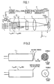
- FIG. 1 is a diagram showing the structure of an embodiment of a wavelength selective switch according to the present invention.
- the wavelength selective switch of the present embodiment comprises for example: a fiber collimator array 10 serving as an optical input/output section; a diffraction grating 1 serving as a spectroscopic section; a condenser lens 2; a mirror array 3 in which a MEMS mirror, which is a plurality of movable mirrors, is arranged; an MEMS mirror drive circuit 4 serving as a movable mirror driving section; an optical circulator 5 serving as a reflected light extracting section; a channel monitor 6 serving as a reflected light monitor section; and a control circuit 7 serving as a control unit.
- the three-dimensional structure of the optical system of the present wavelength selective switch is for example the same as in the conventional case as shown in FIG. 16 described above.
- the fiber collimator array 10 has one input fiber 11 IN , M output fibers 11 OUT (#1) to 11 OUT (#M), and M+1 collimator lenses 12, one corresponding to each of the fibers.
- the input fiber 11 IN and the output fibers 11 OUT (#1) to 11 OUT (#M) are arranged side by side in the same direction (Y axis direction in a rectangular coordinate system as shown at the bottom right of FIG. 1).
- An optical circulator 5 is connected to one end of the input fiber 11 IN , and a WDM light L IN containing wavelength channels Ch1 to ChN (N channels of optical signals with mutually different wavelengths) is input thereto via the optical circulator 5.
- the other end of the input fiber 11 1N has a typical construction in which the ferrule end face is ground diagonally as shown in the top of FIG. 2 for example, and an AR (Anti-Reflection) coating is applied to the end face so that reflection of light at the fiber end face is prevented.
- the angle of inclination of the ferrule end face is 6 to 8 degrees.
- Each of the lights for which the wavelength channels Ch1 to ChN of the WDM light L IN has been selected as desired and separated by the optical system comprising the diffraction grating 1, the condenser lens 2, and the mirror array 3, are injected into each of the output fibers 11 OUT (#1) to 11 OUT (#M) via corresponding collimator lenses 12.
- the construction of the optical injection end of each of the output fibers 11 OUT (#1) to 11 OUT (#M) is such that the ferrule end face is ground vertically as shown for example in the bottom of FIG. 2, and no AR coating is applied to the end face, so that part of the light injected via a collimator lens 12 from the above-described optical system is reflected at the fiber end face, and returned to the original optical path.
- the reflection ratio at the end face of each of the output fibers 11 OUT (#1) to 11 OUT (#M) is approximately 4% (-14dB).
- the lights transmitted through the end faces of each of the output fibers 11 OUT (#1) to 11 OUT (#M) are output lights L OUT (#1) to L OUT (#M), and the reflected lights are reflected lights L R (#1) to L R (#M).
- the symbols #1 to #M in the brackets denote the output port numbers of the present wavelength selective switch.
- the diffraction grating 1 is a transmission type diffraction grating for separating, depending on their wavelengths, wavelength channels Ch1 to ChN contained in the WDM light L IN that is output from the input fiber 11 IN , and made into parallel lights by the collimator lenses 12, in a different direction (X axis direction) from the arrangement direction (Y axis direction) of the fiber collimator array 10.
- a transmission type diffraction grating 1 is used.
- the condenser lens 2 is a typical lens for focusing each of the wavelength channels Ch1 to ChN separated in the X axis direction by transmission through the diffraction grating 1, onto corresponding MEMS mirrors in the mirror array 3.
- the mirror array 3 has N MEMS mirrors 3(Ch1) to 3(ChN) arranged such that each reflecting surface is located at the focal point of each of the wavelength channels Ch1 to ChN which are transmitted through the condenser lens 2 (refer to FIG. 16).
- the MEMS mirrors 3(Ch1) to 3(ChN) are micro mirrors formed by using a micromachining (Micro Electro Mechanical System: MEMS) technique, and have a construction in which the angles of the reflecting surfaces can be controlled freely in accordance with drive voltages V(Ch1) to V(ChN) output from the MEMS mirror drive circuit 4.
- MEMS Micro Electro Mechanical System
- each of the MEMS mirrors 3(Ch1) to 3(ChN) are controlled to predetermined angles corresponding to the location of any one of the output ports #1 to #M, as set in the output addresses of the wavelength channels Ch1 to ChN to be injected.
- the wavelength channels Ch1 to ChN, reflected by the respective MEMS mirrors 3(Ch1) to 3(ChN) pass through the condenser lens 2 and the diffraction grating 1 in order, and are respectively guided to the target output ports #1 to #M.
- FIG. 1 shows a wavelength channel path guided to output port #3, as an example of a wavelength channel path guided to an output port.
- the wavelength channels Ch1 to ChN guided to the respective target output ports #1 to #M are output from each of the output fibers 11 OUT (#1) to 11 OUT (#M) as the output lights L OUT (#1) to L OUT (#M) of the wavelength selection switch, except for reflected lights L R (#1) to L R (#M) that are reflected by the vertical end faces (refer to the bottom of FIG. 2) of the output fibers 11 OUT (#1) to 11 OUT (#M).
- the reflected lights L R (#1) to L R (#M) travel along the optical paths through which they were transmitted, in the reverse direction, and are thus combined, and reflected light L R containing components corresponding to each of the wavelength channels Ch1 to ChN is returned to the input port (input fiber 11 IN ).
- the optical circulator 5 here has three ports, and transmits a WDM light L IN input to a first port to a second port to which the input fiber 11 IN is connected, in one direction, and transmits the reflected light L R returned to the second port from the input fiber 11 IN to a third port to which the channel monitor 6 is con nected, in one direction.
- the channel monitor 6 measures powers P(Ch1) to P(ChN) of the components corresponding to each of the wavelength channels Ch1 to ChN, which are contained in the reflected light L R output from the third port of the optical circulator 5, and outputs a signal indicating the measurement results to the control circuit 7.
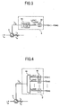
- FIG. 3 and FIG. 4 are block diagrams showing specific structural examples of the channel monitor 6. However, this does not mean that the channel monitor used for the present invention is limited to these structural examples.
- the reflected light L R from the optical circulator 5 is input to a tunable filter 6A, whose transmission band is variable, and any one of the lights L R (Ch1) to L R (ChN) corresponding to each of the wavelength channels contained in the reflected light L R is extracted, and its optical power is measured by a photo detector (PD) 6B.
- a photo detector PD
- the transmission wavelength of the tunable filter 6A by switching the transmission wavelength of the tunable filter 6A by time sharing corresponding to each of the wavelength channels, the powers of the lights corresponding to all of the wavelength channels contained in the reflected light L R are detected by the photo detector 6B.
- the reflected light L R from the optical circulator 5 is input to a demultiplexer 6C, and separated according to its wavelengths.
- Lights L R (Ch1) to L R (ChN) corresponding to each of the wavelength channels, which are output from respective output ports of the demultiplexer 6C, are received by photo detectors (PD) 6D1 to 6DN, provided corresponding to each, and the respective powers are detected.
- the control circuit 7 generates a signal CONT for feedback control of the angles of the reflecting surfaces of the MEMS mirrors 3(Ch1) to 3(ChN) corresponding to each of the wavelength channels on the mirror array 3, based on the optical powers P(Ch1) to P(ChN) monitored by the channel monitor 6, such that each of the powers is at a maximum, and outputs it to a MEMS mirror drive circuit 4.
- the MEMS mirror drive circuit 4 optimizes the drive voltages V(Ch1) to V(ChN) applied to each of the MEMS mirrors 3(Ch1) to 3(ChN), in accordance with the control signal CONT from the control circuit 7.
- the light L R that returns to the input port is separated by the optical circulator 5 located in the input section, the powers P(Ch1) to P(ChN) of the lights corresponding to each of the wavelength channels Ch1 to ChN are monitored by the channel monitor 6, and feedback control of each of the MEMS mirrors 3(Ch1) to 3(ChN) is performed based on the monitored result.
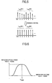
- the control circuit 7 determines that the angles of the reflecting surfaces of each of the MEMS mirrors corresponding to the wavelength channels Ch2 to Ch4, and Ch6 to Ch8 are shifted from their optimum values, and feedback control of the corresponding MEMS mirrors is performed such that the monitored value of each of the reflected light powers is at its maximum as shown at the bottom of FIG. 5.
- the feedback control aims to optimize the drive voltage using the voltage V TARGET , at which the reflected light power is at its maximum, as a control target, in the case where the drive voltages V(Ch1) to V(ChN) of the MEMS mirrors, and each of the reflected light powers P(Ch1) to P(ChN), change according to the relationship as shown for example in FIG 6.
- VOA variable optical attenuator
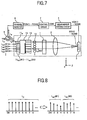
- FIG. 7 is a diagram showing the structure of a wavelength selective switch according to this other embodiment.
- the wavelength selective switch of the present embodiment is provided with a block 13 for securing the ferrules of each of the input fiber 11 IN and the output fibers 11 OUT (#1) to 11 OUT (#M) in a predetermined location, in the structure shown in FIG. 1, and an array waveguide 14, in which optical guided wave paths are formed corresponding to the input fiber 11 IN and each of the output fibers 11 OUT (#1) to 11 OUT (#M), is provided between the block 13 and the collimator lens 12.
- the structures other than those described above are the same as in the case shown in FIG. 1, and hence their descriptions are omitted here.
- the block 13 forms an input/output fiber array arranged in a single direction (Y axis direction), by forming for example parallel V slots at a predetermined spacing in advance, and laying the ferrules of the input fiber 11 IN , and each of the output fibers 11 OUT (#1) to 11 OUT (#M), in the V slots.
- the vertically ground ferrule end faces (refer to the bottom of FIG. 2) of each of the output fibers 11 OUT (#1) to 11 OUT (#M) are placed side by side on one side face (right side face in FIG. 7) of the block 13, and the array waveguide 14 is placed such that it makes contact with that side face of the block 13.
- the crosshatched parts of the block 13 as shown in FIG. 7 are the ferrule end faces of each of the output fibers 11 OUT (#1) to 11 OUT (#M), that is, they illustrate schematically the locations corresponding to reflection devices.
- each of the optical guided wave paths corresponding to the input fiber 11 IN and each of the output fibers 11 OUT (#1) to 11 OUT (#M) is connected to a corresponding end face of one of the input/output fibers located on one side face of the block 13.
- the collimator lenses 12 are located close to the other end faces of each of the optical guided wave paths, and lights input and output between the input fiber 11 IN , the output fibers 11 OUT (#1) to 11 OUT (#M), and each of the collimator lenses 12 are transmitted via corresponding optical guided wave paths in the array waveguide 14.
- a WDM light L IN having a flat wavelength characteristic, in which the powers of each of the wavelength channels Ch1, Ch2, etc. are identical, is input to the wavelength selective switch
- the light L OUT (#1) output from the output port #1 of the wavelength selective switch has wavelength characteristics in which the powers of the wavelength channels Ch1 to ChN are reduced gradually according to their wavelengths
- the light L OUT (#2) output from the output port #2 has wavelength characteristics in which the powers are different between odd and even numbered wavelength channels.
- the angles of the reflecting surfaces of respectively corresponding MEMS mirrors 3(Ch1), 3(Ch5), 3(Ch7) are optimized such that the optical powers reflected by the mirror array 3, and coupled to the cores of the target output fibers 11(#1) and 11(#2), are at the maximum.
- the wavelength selective switch functions as a variable optical attenuator for each of the wavelength channels of the WDM light L IN .
- a wavelength selective switch used as a variable optical attenuator in the case where the structure of the present invention shown in FIG. 1 is applied, that is, a structure in which parts of the lights guided to each of the output fibers 11 OUT (#1) to 11 OUT (#M) passing through the collimator lenses 12 are reflected by each of the output fiber end faces, and the reflected and returned lights are monitored on the input side, by shifting the angles of the reflecting surfaces of the MEMS mirrors from their optimum values, since the lights (loss components that are not coupled inside the cores) that reach the cladding outside the cores on the output fiber end faces are also reflected by the respective fiber end faces, and returned to the input side, it is difficult to accurately monitor the powers of the lights L OUT (#1) to L OUT (#M) output from each of the output ports, on the input side.
- a wavelength selective switch used as a variable optical attenuator associated with a WDM light similarly to the case of the aforementioned embodiment shown in FIG. 1, it is possible to accurately monitor the power of the lights L OUT (#1) to L OUT (#M) output from each of the output ports #1 to #M, using a simple structure. That is, by applying the monitor structure of the present invention to the case where the wavelength selective switch is used as a variable optical attenuator, it is possible to accurately monitor the optical attenuation amount associated with each wavelength channel. Furthermore, by feedback control of the angles of the reflecting surfaces of each of the MEMS mirrors 3(Ch1) to 3(ChN) based on the monitored result, it is possible to reliably guide the wavelength channels whose powers are adjusted to preset levels, to the target output ports.
- the structure of the present invention is effective also in the case where, when the wavelength characteristics of the WDM light L IN input to the wavelength selective switch are not flat, for example as shown at the left side of FIG.
- FIG. 10 is a diagram showing a modified example of a wavelength selective switch corresponding to the above-described case.
- an optical circulator 5' having four ports is connected to an input fiber 11 IN such that the wavelength characteristics of an input WDM light L IN can also be monitored, and the angles of the reflecting surfaces of each of the MEMS mirrors 3(Ch1) to 3(ChN) are feedback controlled according to the relationship between the input powers of each of the wavelength channels Ch1 to ChN and their relative output powers.
- the WDM light L IN input to a first port of the optical circulator 5' is output from a second port, part of it is branched as an input monitor light and transmitted to a channel monitor 8 serving as an input monitor section, and the remainder of the WDM light L IN is totally reflected by a reflector 9, and returned to the second port.
- the WDM light L IN returned to the second port is applied to the input fiber 11 IN from a third port, and transmitted to the optical system of the wavelength selective switch similarly to the case of the embodiment shown in FIG. 7.
- a control circuit 7 outputs to a MEMS mirror drive circuit 4, a signal CONT for filter control of the angles of the reflecting surfaces of the MEMS mirrors 3(Ch1) to 3(ChN) corresponding to each of the wavelength channels, such that the WDM lights L OUT (#1) to L OUT (#M) output from each of the output ports have desired wavelength characteristics, based on the input powers P IN (Ch1) to P IN (ChN) of each of the wavelength channels Ch1 to ChN monitored by the channel monitor 8 on the input side, and the optical powers P OUT (Ch1) to P OUT (ChN) corresponding to each of the wavelength channels Ch1 to ChN monitored by the channel monitor 6 on the output side.
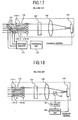
- FIG. 11 is a diagram showing the structure of a wavelength selective switch according to this other embodiment. Furthermore, FIG. 12 is a perspective view showing the arrangement of the optical system of the wavelength selective switch of FIG. 11.
- each of the input fibers 11 IN (#1) to 11 IN (#4) of the fiber collimator array 10' four optical circulators 5(#1) to 5(#4), and four channel monitors 6(#1) to 6(#4) are provided.
- the structures other than the above-described fiber collimator array 10', input side mirror array 3 IN , output side mirror array 3 OUT , optical circulators 5(#1) to 5(#4), and channel monitors 6(#1) to 6(#4) are the same as the aforementioned structures shown in FIG. 1. Therefore, their descriptions are omitted here.
- one example of a 4 x 4 (four inputs, four outputs) wavelength selective switch is described.
- the present invention is not limited to this, and it is possible to set the number of input and output ports as desired.
- Each of the input fibers 11 IN (#1) to 11 IN (#4) of the fiber collimator array 10' has a typical structure in which the ferrule end faces are ground diagonally similarly to the aforementioned structural example shown at the top of FIG. 2, and an AR coating is applied to the end faces, so that reflection of light at the fiber end faces is prevented.
- each of the output fibers 11 OUT (#1) to 11 OUT (#4) has a structure in which the ferrule end faces are ground vertically similarly to the aforementioned structural example shown at the bottom of FIG. 2, and no AR coating is applied to the end faces, so that part of the light guided via the collimator lenses 12 is reflected at the fiber end faces, and returned to the original optical path.
- the WDM lights L IN (#1) to L IN (#4) output from each of the input fibers 11 IN (#1) to 11 IN (#4) are transmitted to a diffraction grating 1 via the collimator lenses 12, and separated into wavelength channels Ch1(#1) to ChN(#1), Ch1(#2) to ChN(#2), Ch1(#3) to ChN(#3), and Ch1(#4) to ChN(#4) contained in each, and then each of the wavelength channels Ch1(#1) to ChN(#4) is focused by a condenser lens 2, and transmitted to the input side mirror array 3 IN .
- the input side mirror array 3 IN has 4 x N MEMS mirrors 3 IN (#1, Ch1) to 3 IN (#1, ChN), 3 IN (#2, Ch1) to 3 IN (#2, ChN), 3 IN (#3, Ch1) to 3 IN (#3, ChN), and 3 IN (#4, Ch1) to 3 IN (#4, ChN), which are arranged such that the reflecting surfaces are positioned at the focal locations of each of the wavelength channels Ch1(#1) to ChN(#4) passing through the condenser lens 2 (refer to FIG 12).
- the input side mirror array 3 IN is here positioned such that it is at an angle of 45° with respect to the Z axis direction.
- Each of the MEMS mirrors 3 IN (#1, Ch1) to 3 IN (#4, ChN) has a structure in which the angles of the reflecting surfaces can be controlled freely in accordance with the drive voltages V IN (#1, Ch1) to V IN (#4, ChN) output from the MEMS mirror drive circuit 4.
- the angles of the reflecting surfaces of each of the MEMS mirrors 3 IN (#1, Ch1) to 3 IN (#4, ChN) are controlled in agreement with the locations of the MEMS mirrors of the output side mirror array 3 OUT , corresponding to any one of the output ports set in the output addresses of the wavelength channels Ch1(#1) to ChN(#4) to be injected.
- the output side mirror array 3 IN is arranged such that it is at an angle of - 45° with respect to the Z axis direction, and has 4xN MEMS mirrors 3 OUT (#1, Ch1) to 3 OUT (#1, ChN), 3 OUT (#2, Ch1) to 3 OUT (#2, ChN), 3 OUT (#3, Ch1) to 3 OUT (#3, ChN), and 3 OUT (#4, Ch1) to 3 OUT (#4, ChN) for reversing the direction of travel of each of the wavelength channels Ch1(#1) to ChN(#4) reflected by the input side mirror array 3 IN , toward the target output ports (refer to FIG. 12).
- each of the MEMS mirrors 3 OUT (#1, Ch1) to 3 OUT (#4, ChN) are controlled in accordance with the drive voltages V OUT (#1, Ch1) to V OUT (#4, ChN) output from the MEMS mirror drive circuit 4.
- Each of the optical circulators 5(#1) to 5(#4) has three ports similarly to the aforementioned optical circulator 5 shown in FIG. 1, and transmits in one direction WDM lights L IN (#1) to L IN (#4) input to the first port, to the second port to which each of the input fibers 11 IN (#1) to 11 IN (#4) are connected, and transmits in one direction the reflected light L R returned to the second port from each of the input fibers 11 IN (#1) to 11 IN (#4), to the third port to which each of the channel monitors 6(#1) to 6(#4) are connected.
- the channel monitors 6(#1) to 6(#4) measure powers P #1 (Ch1) to P #1 (ChN), P #2 (Ch1) to P #2 (ChN), P #3 (Ch1) to P #3 (ChN), and P #4 (Ch1) to P #4 (ChN) of the optical components corresponding to each of the wavelength channels Ch1 to ChN, which are contained in the reflected light L R output from the third port of each of the optical circulators 5, and outputs a signal indicating the measurement results to the control circuit 7.
- P #1 (Ch1) to P #1 (ChN) P #2 (Ch1) to P #2 (ChN)
- P #3 (Ch1) to P #3 (ChN) P #4 (Ch1) to P #4 (ChN) of the optical components corresponding to each of the wavelength channels Ch1 to ChN, which are contained in the reflected light L R output from the third port of each of the optical circulators 5, and outputs a signal indicating the measurement results to the control circuit 7.
- P #1 (Ch1) to P #1 (ChN) P #2 (Ch1) to P #2 (Ch
- the control circuit 7 generates a signal CONT for feedback controlling the angles of the reflecting surfaces of the MEMS mirrors 3 IN (#1, Ch1) to 3 IN (#4,ChN) corresponding to the input side mirror array 3 IN , and the angles of the reflecting surfaces of the MEMS mirrors 3 OUT (#1, Ch1) to 3 OUT (#4,ChN) corresponding to the output side mirror array 3 OUT , based on the powers P #1 (Ch1) to P #4 (ChN) of the reflected lights monitored by each of the channel monitors 6(#1) to 6(#4), such that each of the powers is at the maximum.
- the MEMS mirror drive circuit 4 optimizes the drive voltages V IN (#1, Ch1) to V IN (#4, ChN) applied to the input side MEMS mirrors 3 IN (#1, Ch1) to 3 IN (#4, ChN), and drive voltages V OUT (#1, Ch1) to V OUT (#4, ChN) applied to the output side MEMS mirrors 3 OUT (#1, Ch1) to 3 OUT (#4, ChN), in accordance with the control signal CONT from the control circuit 7.
- the wavelength channel ChN(#2) of the WDM light L IN (#2) is guided to the target output fiber 11 OUT (#3) by being reflected in order by the input side MEMS mirror 3 IN (#2, ChN) and the output side MEMS mirror 3 OUT (#3, ChN), the angles of whose reflecting surfaces are set to predetermined initial values according to the setting of the output addresses. Furthermore, similarly to this, the wavelength channel ChN(#4) of the WDM light L IN (#4) is reflected by the input side MEMS mirror 3 IN (#4, ChN) and the output side MEMS mirror 3 OUT (#1, ChN) in order, and guided to the target output fiber 11 OUT (#1)
- Part of the wavelength channel ChN(#2) reaching the output fiber 11 OUT (#3) is reflected by the output fiber end face, and the reflected light L R (#3, ChN) is returned to the input side.
- the reflected light L R (#3, ChN) is transmitted from the optical circulator 5(#2) to the channel monitor 6(#2), and its power P #2 (ChN) is monitored.
- part of the wavelength channel ChN(#4) reaching the output fiber 11 OUT (#1) is similarly reflected by the output fiber end face, and the reflected light L R (#1, ChN) is returned to the input side.
- the reflected light L R (#1, ChN) is transmitted from the optical circulator 5(#4) to the channel monitor 6(#4), and its power P #4 (ChN) is monitored.
- control circuit 7 In the control circuit 7 receiving the monitored result from each of the channel monitors 6(#2), and 6(#4), by reference to the setting information of the output address of the wavelength channel ChN(#2), corresponding MEMS mirrors 3 IN (#2, ChN), and 3 OUT (#3, ChN) are specified on the input side and output side, and the angles of each of the reflecting surfaces are feedback controlled such that the monitored value P #2 (ChN) from the channel monitor 6(#2) is at the maximum.
- corresponding MEMS mirrors 3 IN (#4, ChN) and 3 OUT (#1, ChN) are specified on the input side and output side, and the angles of each of the reflecting surfaces are feedback controlled such that the monitored value P #4 (ChN) from the channel monitor 6(#4) is at the maximum.
- an example of an optical system is shown in which the input side mirror array 3 IN and the output side mirror array 3 OUT are arranged symmetrically by tilting them by ⁇ 45° with respect to the Z axis direction.
- the structure of the optical system of a wavelength selective switch having a plurality of input/output ports is not limited to the above-described example.
- a wavelength selective switch since the construction is such that parts of the lights injected to a plurality of output fibers are reflected by respective fiber end faces, and returned to the input side, the reflection attenuation characteristics seen from the output port side of the wavelength selective switch are deteriorated due to reflection at the output fiber end face, which is sometimes a problem. In such a case, for example by applying the structure as shown in FIG. 13, it is possible to prevent deterioration of the reflection attenuation characteristics.
- the wavelength selective switch of FIG. 13 is provided with output fibers 15 OUT (#1) to 15 OUT (#M) having end faces ground diagonally, and to which an AR coating is applied similarly to the input fiber 11 IN , and an isolator array 21 in which small size isolators are placed side by side is inserted between the output fibers 15 OUT (#1) to 15 OUT (#M) and collimator lenses 12, corresponding to each of the output fibers 15 OUT (#1) to 15 OUT (#M).
- a reflection section 21A for reflecting part of the light injected is formed on the end face of the isolator array 21 on the collimator lenses 12 side.
- a reflection section 21A for reflecting part of the light injected is formed on the end face of the isolator array 21 on the collimator lenses 12 side.
- a small size isolator used for this type of isolator array 21 it is possible to use a "miniature surface mount type optical isolator" manufactured by Sumitomo Metal Mining Co., Ltd.
- the isolator array 21 is arranged between the output fibers 15 OUT (#1) to 15 OUT (#M) and the collimator lenses 12.
- the isolator array 21 may be provided between the collimator lenses 12 and the diffraction grating 1.
- Lenses 22 arranged close to the end face of the isolator array 21 focus light transmitted through the diffraction grating 1 onto the input end faces of each of the isolators.
- optical powers P(Ch1) to P(ChN) corresponding to each of the wavelength channels, monitored by the channel monitor 6, are used for feedback control of the MEMS mirrors 3(Ch1) to 3(ChN).
- the present invention is not limited to this.
Landscapes
- Engineering & Computer Science (AREA)
- Computer Networks & Wireless Communication (AREA)
- Mechanical Light Control Or Optical Switches (AREA)
- Optical Communication System (AREA)
Applications Claiming Priority (1)
| Application Number | Priority Date | Filing Date | Title |
|---|---|---|---|
| JP2005061865A JP4476140B2 (ja) | 2005-03-07 | 2005-03-07 | 波長選択スイッチ |
Publications (1)
| Publication Number | Publication Date |
|---|---|
| EP1701580A2 true EP1701580A2 (de) | 2006-09-13 |
Family
ID=36570483
Family Applications (1)
| Application Number | Title | Priority Date | Filing Date |
|---|---|---|---|
| EP05013897A Withdrawn EP1701580A2 (de) | 2005-03-07 | 2005-06-28 | Wellenlängenselektiver MEMS-Schalter |
Country Status (4)
| Country | Link |
|---|---|
| US (1) | US7440648B2 (de) |
| EP (1) | EP1701580A2 (de) |
| JP (1) | JP4476140B2 (de) |
| CN (1) | CN100439957C (de) |
Cited By (8)
| Publication number | Priority date | Publication date | Assignee | Title |
|---|---|---|---|---|
| EP2083308A1 (de) * | 2008-01-28 | 2009-07-29 | Fujitsu Limited | Optische Vorrichtung, optische Kommunikationsvorrichtung und Steuerverfahren für die optische Vorrichtung |
| EP2151703A3 (de) * | 2008-08-08 | 2010-03-24 | Fujitsu Limited | Optisches Modul, optisches Steuerungsverfahren durch das optische Modul, optischer Schalter und optisches Schaltverfahren |
| US8179581B1 (en) | 2007-03-28 | 2012-05-15 | University Of South Florida | Electrostatically-addressed MEMS array system and method of use |
| US20140348464A1 (en) * | 2012-03-19 | 2014-11-27 | Fujitsu Limited | Wavelength selective switch, variable dispersion compensator, optical transmission apparatus, and optical transmission system |
| CN111327975A (zh) * | 2019-10-23 | 2020-06-23 | 华为技术有限公司 | 一种端口检测的方法、光网络设备以及无源光网络系统 |
| EP3988975A1 (de) * | 2020-10-20 | 2022-04-27 | Intel Corporation | Integrierte optische sender-empfänger-schaltung |
| EP3978988A4 (de) * | 2019-10-14 | 2022-08-24 | Huawei Technologies Co., Ltd. | Leistungsentzerrer und anpassungsverfahren dafür |
| US12356127B2 (en) | 2020-05-11 | 2025-07-08 | Huawei Technologies Co., Ltd. | Port detection method and apparatus |
Families Citing this family (72)
| Publication number | Priority date | Publication date | Assignee | Title |
|---|---|---|---|---|
| US7292786B1 (en) * | 2002-09-24 | 2007-11-06 | Avanex Corporation | Method and system for a re-configurable optical multiplexer, de-multiplexer and optical add-drop multiplexer |
| JP4776498B2 (ja) * | 2006-07-14 | 2011-09-21 | 富士通株式会社 | レンズアレイを用いた光学装置 |
| US7702194B2 (en) * | 2006-11-07 | 2010-04-20 | Olympus Corporation | Beam steering element and associated methods for manifold fiberoptic switches |
| US7769255B2 (en) * | 2006-11-07 | 2010-08-03 | Olympus Corporation | High port count instantiated wavelength selective switch |
| US7873246B2 (en) * | 2006-11-07 | 2011-01-18 | Olympus Corporation | Beam steering element and associated methods for manifold fiberoptic switches and monitoring |
| US7720329B2 (en) * | 2006-11-07 | 2010-05-18 | Olympus Corporation | Segmented prism element and associated methods for manifold fiberoptic switches |
| US8131123B2 (en) * | 2006-11-07 | 2012-03-06 | Olympus Corporation | Beam steering element and associated methods for manifold fiberoptic switches and monitoring |
| US8000568B2 (en) * | 2006-11-07 | 2011-08-16 | Olympus Corporation | Beam steering element and associated methods for mixed manifold fiberoptic switches |
| IL181135A (en) * | 2007-02-01 | 2012-04-30 | Eci Telecom Ltd | Method, device and system for managing optical communication networks |
| JP4852491B2 (ja) * | 2007-07-27 | 2012-01-11 | 日本電信電話株式会社 | 光クロスコネクトスイッチ機能部及び光クロスコネクト装置 |
| US8045854B2 (en) * | 2008-02-07 | 2011-10-25 | Jds Uniphase Corporation | M×N wavelength selective optical switch |
| JP5593587B2 (ja) * | 2008-03-05 | 2014-09-24 | 日本電気株式会社 | 波長多重分離方式及び波長多重分離方法 |
| US8625994B2 (en) * | 2008-03-11 | 2014-01-07 | Ciena Corporation | Directionless reconfigurable optical add-drop multiplexer systems and methods |
| US8849115B2 (en) | 2008-03-11 | 2014-09-30 | Ciena Corporation | Directionless optical architecture and highly available network and photonic resilience methods |
| JP5056664B2 (ja) * | 2008-08-08 | 2012-10-24 | 富士通株式会社 | 波長選択光スイッチ |
| JP2010139854A (ja) | 2008-12-12 | 2010-06-24 | Fujitsu Ltd | 波長多重伝送装置及び波長多重伝送方法 |
| JP5599175B2 (ja) * | 2009-10-06 | 2014-10-01 | ジェイディーエス ユニフェイズ コーポレーション | 分散素子、分光装置、及び波長選択スイッチ |
| US8280206B2 (en) | 2009-12-21 | 2012-10-02 | Accelink Technologies Co., Ltd. | WSS with hitless switching |
| JP5446944B2 (ja) | 2010-01-29 | 2014-03-19 | 富士通株式会社 | 光ネットワークおよびその制御方法 |
| US8923667B2 (en) * | 2010-02-12 | 2014-12-30 | Finisar Corporation | Wavelength selective switch with multiple input/output ports |
| JP5563855B2 (ja) * | 2010-03-19 | 2014-07-30 | ジェイディーエス ユニフェイズ コーポレーション | 波長選択スイッチ |
| US8300995B2 (en) | 2010-06-30 | 2012-10-30 | Jds Uniphase Corporation | M X N WSS with reduced optics size |
| US8755651B2 (en) * | 2010-07-26 | 2014-06-17 | Oclaro (North America Inc.) | Tunable optical filters with multiple ports |
| US8755652B2 (en) * | 2010-07-26 | 2014-06-17 | Oclaro Technology Limited | Multi-channel optical signal monitoring device and method |
| US8577192B2 (en) | 2010-07-26 | 2013-11-05 | Oclaro (North America Inc.) | Tunable optical filters with multiple ports |
| US9097580B2 (en) | 2010-07-26 | 2015-08-04 | Ii-Vi Incorporated | Multiport tunable optical filters |
| US8873905B2 (en) | 2010-07-26 | 2014-10-28 | Ii-Vi Incorporated | Reconfigurable optical add-drop multiplexer |
| CN102375180A (zh) * | 2010-08-23 | 2012-03-14 | 深圳新飞通光电子技术有限公司 | 一种基于awg的可调光波长输出装置 |
| TWI514000B (zh) * | 2010-08-31 | 2015-12-21 | Corning Inc | Mems為主監視系統及使用方法 |
| CN101995657A (zh) * | 2010-09-15 | 2011-03-30 | 华为技术有限公司 | 一种光开关的方法及一种光开关 |
| JP5672011B2 (ja) * | 2011-01-04 | 2015-02-18 | 富士通株式会社 | 波長選択スイッチおよび波長ずれ補正方法 |
| CN102135647A (zh) * | 2011-02-21 | 2011-07-27 | 华为技术有限公司 | 光开关系统和信号光的反馈控制方法 |
| JP5651904B2 (ja) * | 2011-04-14 | 2015-01-14 | 独立行政法人産業技術総合研究所 | N×n波長選択スイッチ |
| US8867917B2 (en) * | 2011-06-27 | 2014-10-21 | Finisar Corporation | Optical wavelength selective switch calibration system |
| JP5838639B2 (ja) | 2011-08-02 | 2016-01-06 | 富士通株式会社 | 光伝送装置及び光伝送方法 |
| US8699024B2 (en) | 2011-08-23 | 2014-04-15 | Jds Uniphase Corporation | Tunable optical filter and spectrometer |
| CN102369679B (zh) * | 2011-08-24 | 2014-07-30 | 华为技术有限公司 | 一种多通道光学组件以及测试系统 |
| CA2787565A1 (en) * | 2011-08-24 | 2013-02-24 | Nistica, Inc. | Asymmetric lenslet array |
| CN102483494B (zh) * | 2011-09-09 | 2013-01-23 | 华为技术有限公司 | 光器件、光器件集成方法及光网络系统 |
| JP5750163B2 (ja) * | 2011-09-16 | 2015-07-15 | 日本電信電話株式会社 | 光スイッチ |
| JP5909365B2 (ja) * | 2012-01-05 | 2016-04-26 | 株式会社ミツトヨ | 接触プローブ |
| US8731403B2 (en) * | 2012-02-07 | 2014-05-20 | Ii-Vi Incorporated | Multicast optical switch |
| JP5825162B2 (ja) * | 2012-03-16 | 2015-12-02 | 富士通株式会社 | フロントエンド装置 |
| CN102707387B (zh) * | 2012-06-08 | 2014-05-07 | 武汉邮电科学研究院 | 波长选择开关及切换方法 |
| EP2860571A4 (de) * | 2012-06-11 | 2015-07-08 | Fujitsu Ltd | Optische übertragungsvorrichtung |
| WO2014034144A1 (ja) | 2012-08-30 | 2014-03-06 | 日本電信電話株式会社 | 光信号処理装置 |
| JP5840176B2 (ja) * | 2012-09-07 | 2016-01-06 | 古河電気工業株式会社 | 光スイッチ |
| JP2014074900A (ja) * | 2012-09-13 | 2014-04-24 | Sumitomo Electric Ind Ltd | 波長選択スイッチ |
| CN103969748A (zh) * | 2013-01-30 | 2014-08-06 | 福州高意通讯有限公司 | 一种基于dlp的波长选择开关 |
| CN105229945B (zh) * | 2013-03-20 | 2019-03-19 | 尼斯迪卡有限公司 | 具有集成的信道监测器的波长选择开关 |
| US9755738B2 (en) * | 2013-03-20 | 2017-09-05 | Nistica, Inc. | Crosstalk suppression in a multi-photodetector optical channel monitor |
| CN103281153B (zh) * | 2013-06-20 | 2016-01-20 | 中央民族大学 | 一种基于硅基液晶的m×n端口的可重构光分插复用器 |
| CN104238025B (zh) * | 2013-06-21 | 2017-12-29 | 华为技术有限公司 | 光路处理方法和装置 |
| JP2016527545A (ja) * | 2013-06-27 | 2016-09-08 | オプリンク コミュニケーションズ エルエルシー | Memsファイバ光スイッチ |
| US9338528B2 (en) * | 2013-07-18 | 2016-05-10 | Globalfoundries Inc. | Optimal positioning of reflecting optical devices |
| EP3043495B1 (de) * | 2013-09-27 | 2017-11-22 | Huawei Technologies Co., Ltd. | Wellenlängenselektiver schalter und verfahren zur steuerung eines räumlichen phasenmodulators in diesem wellenlängenselektiven schalter |
| CN103558667B (zh) * | 2013-11-19 | 2016-04-13 | 武汉光迅科技股份有限公司 | 一种基于自由空间传输的多播交换光开关 |
| CN103558668B (zh) * | 2013-11-19 | 2016-02-10 | 武汉邮电科学研究院 | 波长选择开关和波长选择方法 |
| CN105223657B (zh) | 2014-05-27 | 2018-07-03 | 华为技术有限公司 | 光开关和波分复用光系统 |
| JP2017152749A (ja) * | 2014-06-30 | 2017-08-31 | 国立大学法人名古屋大学 | 光クロスコネクト装置 |
| JP2016036091A (ja) * | 2014-08-04 | 2016-03-17 | 富士通株式会社 | 伝送装置および光ネットワークシステム |
| WO2019176834A1 (ja) * | 2018-03-13 | 2019-09-19 | 日本電気株式会社 | 光伝送装置及び光伝送方法 |
| CN110730034B (zh) * | 2018-07-16 | 2022-02-25 | 华为技术有限公司 | 频偏处理方法、装置、设备及存储介质 |
| EP3857293B1 (de) * | 2018-09-28 | 2024-04-17 | Magic Leap, Inc. | Projektionssystem mit kollimierendem abtastendem spiegel |
| CN111313130B (zh) * | 2019-11-04 | 2021-03-26 | 华中科技大学 | 一种用于切换大功率电子回旋波传输方向的波导开关 |
| JP7544124B2 (ja) * | 2020-07-06 | 2024-09-03 | 日本電信電話株式会社 | 波長クロスコネクト装置及び波長クロスコネクト方法 |
| CN114063215B (zh) * | 2020-07-30 | 2023-08-22 | 华为技术有限公司 | 一种波长选择开关和光交换设备、系统 |
| US11910134B2 (en) * | 2020-11-06 | 2024-02-20 | Google Llc | Optical link diagnostic system |
| CN112596167A (zh) * | 2020-12-15 | 2021-04-02 | 上海钜成锐讯科技有限公司 | 一种具有波长漂移检测功能的高隔离度波长选择开关 |
| CN116847228B (zh) * | 2023-07-06 | 2025-10-21 | 中国电信股份有限公司技术创新中心 | 数据传输方法、装置、网络系统、计算机设备和存储介质 |
| US20250254449A1 (en) * | 2024-02-01 | 2025-08-07 | Huawei Technologies Co., Ltd. | In-band operations and management for optical switch |
| CN120722506A (zh) * | 2024-03-29 | 2025-09-30 | 华为技术有限公司 | 光交叉连接设备 |
Citations (3)
| Publication number | Priority date | Publication date | Assignee | Title |
|---|---|---|---|---|
| JP2000347065A (ja) | 1999-05-13 | 2000-12-15 | Lucent Technol Inc | 光装置 |
| JP2001330865A (ja) | 2000-05-19 | 2001-11-30 | Nec Corp | 波長可変型の光フィルタ |
| US6549699B2 (en) | 2001-03-19 | 2003-04-15 | Capella Photonics, Inc. | Reconfigurable all-optical multiplexers with simultaneous add-drop capability |
Family Cites Families (16)
| Publication number | Priority date | Publication date | Assignee | Title |
|---|---|---|---|---|
| JPH0588216A (ja) | 1991-09-26 | 1993-04-09 | Asahi Glass Co Ltd | 音響光学光スイツチ及び分布型光フアイバセンサ |
| JP2755147B2 (ja) | 1993-12-27 | 1998-05-20 | 日本電気株式会社 | 光増幅器の光出力自動低下回路 |
| JPH07307764A (ja) * | 1994-03-18 | 1995-11-21 | Fujitsu Ltd | 光並列受信装置に用いられるデータ識別回路、光並列受信装置、光並列伝送装置及び光伝送ファイバの端末構造 |
| US6263123B1 (en) * | 1999-03-12 | 2001-07-17 | Lucent Technologies | Pixellated WDM optical components |
| US6449406B1 (en) * | 1999-05-28 | 2002-09-10 | Omm, Inc. | Micromachined optomechanical switching devices |
| US6404251B1 (en) * | 2000-03-27 | 2002-06-11 | Linear Technology Corporation | Systems and methods for linearly varying a pulse-width modulation signal with a control signal |
| US6487336B1 (en) * | 2000-10-11 | 2002-11-26 | General Photonics Corporation | WDM channel equalization and control |
| JP3937403B2 (ja) * | 2001-03-19 | 2007-06-27 | カペラ フォトニクス インコーポレイテッド | 再構成可能型光アドドロップ多重化装置 |
| US20030090756A1 (en) * | 2001-09-25 | 2003-05-15 | Cidra Corporation | Optical channel monitor having an array of micro-mirrors |
| US6522118B1 (en) * | 2001-04-18 | 2003-02-18 | Linear Technology Corporation | Constant-current/constant-voltage current supply |
| US6614954B2 (en) * | 2001-10-24 | 2003-09-02 | Transparent Networks, Inc. | Feedback control system for a MEMS based optical switching fabric |
| US6922500B2 (en) * | 2001-10-24 | 2005-07-26 | Intel Corporation | Optical configuration for optical fiber switch |
| JP4232781B2 (ja) * | 2003-04-25 | 2009-03-04 | 株式会社ニコン | アッテネータ装置および光スイッチング装置 |
| US20050074204A1 (en) * | 2003-10-02 | 2005-04-07 | Gordon Wilson | Spectral plane method and apparatus for wavelength-selective optical switching |
| US7521660B2 (en) * | 2004-04-15 | 2009-04-21 | Sumitomo Electric Industries, Ltd. | Optical signal processor and optical signal processing method for processing optical signals in optical communications systems |
| JP4500720B2 (ja) * | 2005-03-29 | 2010-07-14 | 富士通株式会社 | 光スイッチ |
-
2005
- 2005-03-07 JP JP2005061865A patent/JP4476140B2/ja not_active Expired - Lifetime
- 2005-06-22 US US11/157,985 patent/US7440648B2/en not_active Expired - Fee Related
- 2005-06-28 EP EP05013897A patent/EP1701580A2/de not_active Withdrawn
- 2005-07-15 CN CNB200510084410XA patent/CN100439957C/zh not_active Expired - Fee Related
Patent Citations (3)
| Publication number | Priority date | Publication date | Assignee | Title |
|---|---|---|---|---|
| JP2000347065A (ja) | 1999-05-13 | 2000-12-15 | Lucent Technol Inc | 光装置 |
| JP2001330865A (ja) | 2000-05-19 | 2001-11-30 | Nec Corp | 波長可変型の光フィルタ |
| US6549699B2 (en) | 2001-03-19 | 2003-04-15 | Capella Photonics, Inc. | Reconfigurable all-optical multiplexers with simultaneous add-drop capability |
Cited By (14)
| Publication number | Priority date | Publication date | Assignee | Title |
|---|---|---|---|---|
| US8179581B1 (en) | 2007-03-28 | 2012-05-15 | University Of South Florida | Electrostatically-addressed MEMS array system and method of use |
| EP2083308A1 (de) * | 2008-01-28 | 2009-07-29 | Fujitsu Limited | Optische Vorrichtung, optische Kommunikationsvorrichtung und Steuerverfahren für die optische Vorrichtung |
| EP2151703A3 (de) * | 2008-08-08 | 2010-03-24 | Fujitsu Limited | Optisches Modul, optisches Steuerungsverfahren durch das optische Modul, optischer Schalter und optisches Schaltverfahren |
| US8441706B2 (en) | 2008-08-08 | 2013-05-14 | Fujitsu Limited | Optical module, optical control method by optical module, optical switch, and optical switching method |
| US9588297B2 (en) | 2012-03-19 | 2017-03-07 | Fujitsu Limited | Wavelength selective switch, variable dispersion compensator, optical transmission apparatus, and optical transmission system |
| EP2830238A4 (de) * | 2012-03-19 | 2015-11-11 | Fujitsu Ltd | Wellenlängenselektiver schalter, variabler dispersionskompensator, überwachungsvorrichtung, überwachungsverfahren, optische übertragungsvorrichtung und optisches übertragungssystem |
| US20140348464A1 (en) * | 2012-03-19 | 2014-11-27 | Fujitsu Limited | Wavelength selective switch, variable dispersion compensator, optical transmission apparatus, and optical transmission system |
| EP3978988A4 (de) * | 2019-10-14 | 2022-08-24 | Huawei Technologies Co., Ltd. | Leistungsentzerrer und anpassungsverfahren dafür |
| US12085760B2 (en) | 2019-10-14 | 2024-09-10 | Huawei Technologies Co., Ltd. | Power equalizer and adjustment method therefor |
| CN111327975A (zh) * | 2019-10-23 | 2020-06-23 | 华为技术有限公司 | 一种端口检测的方法、光网络设备以及无源光网络系统 |
| CN111327975B (zh) * | 2019-10-23 | 2021-06-15 | 华为技术有限公司 | 一种端口检测的方法、光网络设备以及无源光网络系统 |
| US12107666B2 (en) | 2019-10-23 | 2024-10-01 | Huawei Technologies Co., Ltd. | Port detection method, optical network device, and passive optical network system |
| US12356127B2 (en) | 2020-05-11 | 2025-07-08 | Huawei Technologies Co., Ltd. | Port detection method and apparatus |
| EP3988975A1 (de) * | 2020-10-20 | 2022-04-27 | Intel Corporation | Integrierte optische sender-empfänger-schaltung |
Also Published As
| Publication number | Publication date |
|---|---|
| CN1831574A (zh) | 2006-09-13 |
| US20060198583A1 (en) | 2006-09-07 |
| CN100439957C (zh) | 2008-12-03 |
| JP2006243571A (ja) | 2006-09-14 |
| JP4476140B2 (ja) | 2010-06-09 |
| US7440648B2 (en) | 2008-10-21 |
Similar Documents
| Publication | Publication Date | Title |
|---|---|---|
| US7440648B2 (en) | Wavelength selective switch | |
| CA2392704C (en) | System and method of optical switching | |
| USRE39411E1 (en) | Reconfigurable all-optical multiplexers with simultaneous add-drop capability | |
| US6898348B2 (en) | Spectral power equalizer for wavelength-multiplexed optical fiber communication links | |
| AU2014235949B2 (en) | Wavelength selective switch having integrated channel monitor | |
| US6631222B1 (en) | Reconfigurable optical switch | |
| US20090220233A1 (en) | Wavelength selective switch having distinct planes of operation | |
| US8693819B2 (en) | Method and system for switching optical channels | |
| WO2000039626A1 (en) | Wavelength selective optical switch | |
| EP0571379A1 (de) | Durchstimmbare optische filter | |
| US7340126B2 (en) | Wavelength selective optical switch | |
| US7574078B2 (en) | Reconfigurable optical switch | |
| US6792210B1 (en) | Hybrid optical add/drop multiplexing devices | |
| WO2004005993A1 (en) | Dynamic multifunction, multichannel optical device | |
| US20030202741A1 (en) | Dynamically reconfigurable optical add/drop multiplexer | |
| US7062174B2 (en) | Wavelength division multiplexing add-drop multiplexer using an optical tapped delay line | |
| EP1841277A2 (de) | Multiportschalter für einen optischen Leistungsmonitor | |
| US6636657B1 (en) | Channelized wavelength division multiplex equalizer using reflective attenuators | |
| EP1393107A2 (de) | Rekonfigurierbares optisches add/drop-modul | |
| US20040131309A1 (en) | Tunable optical filter, optical switch, and optical add/drop multiplexer employing linearly variable thin film optical filters | |
| WO2001046731A2 (en) | Reconfigurable add/drop multiplexer for fiber optic networks | |
| US20130114957A1 (en) | Dual path wavelength selective switch | |
| CN118946837A (zh) | 光开关 | |
| WO2005116707A1 (en) | Improved variable optical attenuator | |
| CA2364299A1 (en) | Spectral power equalizer for wavelength-multiplexed optical fiber communication links |
Legal Events
| Date | Code | Title | Description |
|---|---|---|---|
| PUAI | Public reference made under article 153(3) epc to a published international application that has entered the european phase |
Free format text: ORIGINAL CODE: 0009012 |
|
| AK | Designated contracting states |
Kind code of ref document: A2 Designated state(s): AT BE BG CH CY CZ DE DK EE ES FI FR GB GR HU IE IS IT LI LT LU MC NL PL PT RO SE SI SK TR |
|
| AX | Request for extension of the european patent |
Extension state: AL BA HR LV MK YU |
|
| STAA | Information on the status of an ep patent application or granted ep patent |
Free format text: STATUS: THE APPLICATION IS DEEMED TO BE WITHDRAWN |
|
| 18D | Application deemed to be withdrawn |
Effective date: 20091231 |