EP1689054A1 - Support laser à semi-conducteurs - Google Patents
Support laser à semi-conducteurs Download PDFInfo
- Publication number
- EP1689054A1 EP1689054A1 EP06002161A EP06002161A EP1689054A1 EP 1689054 A1 EP1689054 A1 EP 1689054A1 EP 06002161 A EP06002161 A EP 06002161A EP 06002161 A EP06002161 A EP 06002161A EP 1689054 A1 EP1689054 A1 EP 1689054A1
- Authority
- EP
- European Patent Office
- Prior art keywords
- semiconductor laser
- holder
- depressions
- laser
- lower holder
- Prior art date
- Legal status (The legal status is an assumption and is not a legal conclusion. Google has not performed a legal analysis and makes no representation as to the accuracy of the status listed.)
- Withdrawn
Links
Images


Classifications
-
- H—ELECTRICITY
- H01—ELECTRIC ELEMENTS
- H01S—DEVICES USING THE PROCESS OF LIGHT AMPLIFICATION BY STIMULATED EMISSION OF RADIATION [LASER] TO AMPLIFY OR GENERATE LIGHT; DEVICES USING STIMULATED EMISSION OF ELECTROMAGNETIC RADIATION IN WAVE RANGES OTHER THAN OPTICAL
- H01S5/00—Semiconductor lasers
- H01S5/02—Structural details or components not essential to laser action
- H01S5/022—Mountings; Housings
- H01S5/02208—Mountings; Housings characterised by the shape of the housings
- H01S5/02212—Can-type, e.g. TO-CAN housings with emission along or parallel to symmetry axis
-
- H—ELECTRICITY
- H01—ELECTRIC ELEMENTS
- H01S—DEVICES USING THE PROCESS OF LIGHT AMPLIFICATION BY STIMULATED EMISSION OF RADIATION [LASER] TO AMPLIFY OR GENERATE LIGHT; DEVICES USING STIMULATED EMISSION OF ELECTROMAGNETIC RADIATION IN WAVE RANGES OTHER THAN OPTICAL
- H01S5/00—Semiconductor lasers
- H01S5/02—Structural details or components not essential to laser action
- H01S5/022—Mountings; Housings
- H01S5/023—Mount members, e.g. sub-mount members
- H01S5/0232—Lead-frames
-
- H—ELECTRICITY
- H01—ELECTRIC ELEMENTS
- H01S—DEVICES USING THE PROCESS OF LIGHT AMPLIFICATION BY STIMULATED EMISSION OF RADIATION [LASER] TO AMPLIFY OR GENERATE LIGHT; DEVICES USING STIMULATED EMISSION OF ELECTROMAGNETIC RADIATION IN WAVE RANGES OTHER THAN OPTICAL
- H01S5/00—Semiconductor lasers
- H01S5/02—Structural details or components not essential to laser action
- H01S5/024—Arrangements for thermal management
-
- G—PHYSICS
- G11—INFORMATION STORAGE
- G11B—INFORMATION STORAGE BASED ON RELATIVE MOVEMENT BETWEEN RECORD CARRIER AND TRANSDUCER
- G11B7/00—Recording or reproducing by optical means, e.g. recording using a thermal beam of optical radiation by modifying optical properties or the physical structure, reproducing using an optical beam at lower power by sensing optical properties; Record carriers therefor
- G11B7/12—Heads, e.g. forming of the optical beam spot or modulation of the optical beam
- G11B7/22—Apparatus or processes for the manufacture of optical heads, e.g. assembly
-
- H—ELECTRICITY
- H01—ELECTRIC ELEMENTS
- H01S—DEVICES USING THE PROCESS OF LIGHT AMPLIFICATION BY STIMULATED EMISSION OF RADIATION [LASER] TO AMPLIFY OR GENERATE LIGHT; DEVICES USING STIMULATED EMISSION OF ELECTROMAGNETIC RADIATION IN WAVE RANGES OTHER THAN OPTICAL
- H01S5/00—Semiconductor lasers
- H01S5/02—Structural details or components not essential to laser action
- H01S5/022—Mountings; Housings
- H01S5/023—Mount members, e.g. sub-mount members
- H01S5/0231—Stems
Definitions
- the present invention relates to a semiconductor laser holder for holding a semiconductor laser incorporated as a light source in an optical pickup apparatus for reproducing information from and recording information to an optical disc such as a CD or DVD as a recording medium. More particularly, the present invention relates to a semiconductor laser holder for holding a frame-type semiconductor laser.
- the semiconductor laser 20 is roughly composed of: a frame plate 21 that is made of metal and on the top face of which a laser element 23 and a photosensor (unillustrated) are mounted; and a frame package 22 that encloses the laser element 23 from the front, rear, left, and right sides thereof.
- the frame package 22 is widely open upward, and has a light-exit opening 22a formed at the front end thereof to permit the emission of laser light from the laser element 23. From the left and right edges of the frame package 22, heat-sink projections 21a of the frame plate 21 protrude outward. These heat-sink projections 21a permit the heat generated by the laser element 23 and conducted via the frame plate 21 to be dissipated to outside. From the rear end of the frame package 22, a plurality of lead pins 24 protrude outward.
- This semiconductor laser 20 since its laser element 23 is exposed to outside, is usually held in a semiconductor laser holder, and this semiconductor laser holder is fitted to the base member of an optical pickup apparatus. If the semiconductor laser 20 is fitted directly to the base member of an optical pickup apparatus, dust and other foreign matter that managed to enter the optical pickup apparatus may float around or settle on the laser element 23, adversely affecting the accuracy of the laser light. This can be prevented when the semiconductor laser 20 is fitted via a semiconductor laser holder.
- the conventional semiconductor laser holder 101 is composed of a pair of holder members, namely an upper holder member 102 and a lower holder member 103, that are fitted together from above and below.
- These upper and lower holder members 102 and 103 have housing depressions 104 and 105 formed in the faces thereof at which they are fitted together, and the semiconductor laser 20 is housed in those housing depressions 104 and 105.
- the laser light emitted from the laser element 23 through the light-exit opening 22a of the semiconductor laser 20 exits from the housing depressions 104 and 105 through an opening 106 at the front end thereof.
- depressions 107 and 108 are formed to accommodate the heat-sink projections 21a of the frame plate 21 of the semiconductor laser 20.
- the semiconductor laser 20 is held inside the semiconductor laser holder 101. See, for example, JP A 2004-192720.
- the conventional semiconductor laser holder 101 described above suffers from poor heat dissipation, because the heat-sink projections 21a of the frame plate 21 of the semiconductor laser 20 are covered with the upper and lower holder members 102 and 103.
- JP A 2004-192720 mentioned above attempts to improve heat dissipation by holding only part of the heat-sink projections 21a between the upper and lower holder members 102 and 103 while leaving the rest of the heat-sink projections 21a protruding from the upper and lower holder members 102 and 103. This, however, cannot be said to promise much.
- a semiconductor laser holder for holding a frame-type semiconductor laser composed of a frame plate formed of metal and having a laser element mounted on the top face thereof and a frame package formed of resin, formed so as to surround the laser element from the front, rear, left, and right sides thereof, and having a light-exit opening formed at the front end thereof to let laser light from the laser element exit therethrough is provided with an upper holder member and a lower holder member formed of metal, fitted together from above and below, having housing depressions formed in the fitting faces thereof to house the semiconductor laser, and having an opening at the front end thereof to let the laser light exit therethrough.
- the lower holder member has depressions formed in the fitting face thereof to accommodate heat-sink projections of the frame plate protruding from the left and right edges of the frame package of the semiconductor laser
- the upper holder member has elevations formed on the fitting face thereof to fit into the depressions so as to hold the heat-sink projections against the floor faces of the depressions.
- the upper and lower holder members in which elevations and depressions between which to hold the heat-sink projections of the frame plate of the semiconductor laser are formed, are formed of metal having high thermal conductivity.
- the heat generated by the laser element and conducted via the frame plate to the heat-sink projections is conducted further to the upper and lower holder members themselves so as to be then dissipated to outside.
- the elevations and depressions formed in the upper and lower holder members serve to hold, between them, the heat-sink projections, and also serve to position the upper and lower holder members relative to each other.
- the upper and lower holder members be formed of zinc.
- the upper and lower holder members that have been fitted together be fixed together by being bonded together with adhesive applied to the fitting faces thereof.
- the upper and lower holder members that have been fitted together be fixed together by being fastened together with a screw.
- a diffraction grating be housed near the opening.
- the diffraction grating be so housed as to be inclined at a predetermined angle relative to the optical axis of the laser light.
- Fig. 1 is a perspective view of the lower holder member constituting the semiconductor laser holder of a first embodiment of the present invention
- Fig. 1 is a perspective view of the lower holder member constituting the semiconductor laser holder of the first embodiment.
- Fig. 2 is a perspective view of the upper holder member constituting the semiconductor laser holder.
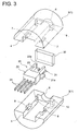
- Fig. 3 is a perspective view showing the exploded state of the semiconductor laser holder.
- Fig. 4 is a perspective view showing the assembled state of the semiconductor laser holder.
- Fig. 5 is a top view showing the assembled state of the semiconductor laser holder, as seen through the upper holder member.
- Fig. 6 is a sectional view along line A-A shown in Fig. 5.
- Fig. 7 is a sectional view along line B-B shown in Fig. 5.
- used as a semiconductor laser is a frame-type semiconductor laser 20 as shown in Figs. 11 and 12 described previously.
- the semiconductor laser holder 1 of this embodiment is composed of a pair of holder members, namely an upper holder member 2 and a lower holder member 3, that are fitted together from above and below.
- the upper and lower holder members 2 and 3 are both formed of metal having high thermal conductivity, and are formed individually by die-casting or machining.
- a preferred material for the upper and lower holder members 2 and 3 is zinc, because it offers satisfactorily high rigidity.
- the upper and lower holder members 2 and 3 have housing depressions 4 and 5 formed in the fitting faces thereof so as to extend from the rear end to the front end thereof, and the semiconductor laser 20 is housed in those housing depressions 4 and 5.
- the laser light emitted from a laser element 23 through a light-exit opening 22a of the semiconductor laser 20 exits from the housing depressions 4 and 5 through an opening 6 at the front end thereof.
- the lead pins 24 of the semiconductor laser 20 protrude.
- depressions 8 are formed to accommodate the heat-sink projections 21a of the frame plate 21 that protrude from the left and right edges of the frame package 22 of the semiconductor laser 20.
- elevations 7 are formed so as to correspond to the depressions 8 of the lower holder member 3.
- the semiconductor laser 20 is housed in the housing depression 5 of the lower holder member 3, with the heat-sink projections 21a of the semiconductor laser 20 accommodated in the depressions 8 of the lower holder member 3.
- the elevations 7 fit into the depressions 8 of the lower holder member 3, and thus the upper and lower holder members 2 and 3 are fitted together.
- the heat-sink projections 21a are held between the roof faces of the elevations 7 of the upper holder member 2 and the floor faces of the depressions 8 of the lower holder member 3, and thus the semiconductor laser 20 is held inside the semiconductor laser holder 1.
- the upper and lower holder members 2 and 3 fitted together are fixed together by being bonded together with adhesive applied to the fitting faces thereof. Alternatively, they may be fixed together by being fastened with a screw.
- grooves 9 and 10 are formed so as to extend perpendicularly to the optical axis of the laser light emitted from the laser element 23 through the light-exit opening 22a of the semiconductor laser 20.
- a diffraction grating 30 is housed.
- the upper and lower holder members 2 and 3 in which the elevations 7 and the depressions 8 between which to hold the heat-sink projections 21a of the frame plate 21 of the semiconductor laser 20 are formed, are formed of metal having high thermal conductivity, the heat generated by the laser element 23 and conducted via the frame plate 21 to the heat-sink projections 21a is conducted further to the upper and lower holder members 2 and 3 themselves so as to be then dissipated to outside. Thus, it is possible to achieve satisfactory heat dissipation without spoiling it.
- the elevations 7 and the depressions 8 formed in the upper and lower holder members 2 and 3 serve to hold, between them, the heat-sink projections 2a, and also serve to position the upper and lower holder members 2 and 3 relative to each other.
- the semiconductor laser 20 is held stably. The same is true when they are fixed together by being fastened together with a screw. Furthermore, since the diffraction grating 30 is housed in the housing depressions 4 and 5 of the upper and lower holder members 2 and 3, near the opening 6, it is possible to prevent undesirable entry of dust and other foreign matter through the opening 6.
- Fig. 8 is a perspective view of the lower holder member constituting the semiconductor laser holder of the second embodiment.
- Fig. 9 is a perspective view of the upper holder member constituting the semiconductor laser holder.
- Fig. 10 is a top view showing the assembled state of the semiconductor laser holder, as seen through the upper holder member.
- such parts as have the same names and serve the same purposes as in Figs. 1 to 7 are identified with common reference numerals, and no overlapping explanations will be repeated.
- the second embodiment is characterized in that it is so structured as to cope with a case where, as the semiconductor laser 20 in the first embodiment, a semiconductor laser is adopted that intrinsically has a large astigmatic difference.
- the grooves 9 and 10 formed in the upper and lower holder members 2 and 3 to house the diffraction grating 30 are inclined at a predetermined angle relative to the optical axis of the laser light emitted from the laser element 23 via the light-exit opening 22a of the semiconductor laser 20. That is, the diffraction grating 30 is so housed as to be inclined at a predetermined angle relative to the optical axis of the laser light.
- the diffraction grating 30 arranged at an angle corrects for the astigmatic difference. Needless to say, it also prevents undesirable entry of dust and other foreign matter through the opening 6.
- the diffraction grating 30 does not necessarily have to be provided inside the housing depressions 4 and 5 of the upper and lower holder members 2 and 3.
- a diffraction grating is separately provided on the base member of the pickup apparatus to which the semiconductor laser holder 1 is fitted. Even in that case, the laser element 23 of the semiconductor laser 20 housed inside the semiconductor laser holder 1 is surrounded by the upper and lower holder members 2 and 3, and is thereby kept dust-free.
Applications Claiming Priority (1)
| Application Number | Priority Date | Filing Date | Title |
|---|---|---|---|
| JP2005000428U JP3110158U (ja) | 2005-02-02 | 2005-02-02 | 半導体レーザー用ホルダ |
Publications (1)
| Publication Number | Publication Date |
|---|---|
| EP1689054A1 true EP1689054A1 (fr) | 2006-08-09 |
Family
ID=36591339
Family Applications (1)
| Application Number | Title | Priority Date | Filing Date |
|---|---|---|---|
| EP06002161A Withdrawn EP1689054A1 (fr) | 2005-02-02 | 2006-02-02 | Support laser à semi-conducteurs |
Country Status (4)
| Country | Link |
|---|---|
| US (1) | US20060171441A1 (fr) |
| EP (1) | EP1689054A1 (fr) |
| JP (1) | JP3110158U (fr) |
| CN (1) | CN1815584A (fr) |
Cited By (2)
| Publication number | Priority date | Publication date | Assignee | Title |
|---|---|---|---|---|
| WO2011063224A3 (fr) * | 2009-11-23 | 2011-09-29 | Seminex Corporation | Système d'assemblage et de mise sous boîtier de lasers à semi-conducteurs |
| US10630038B2 (en) | 2015-08-27 | 2020-04-21 | Trumpf Laser Gmbh | Stress-optimized laser disk mounting systems |
Families Citing this family (4)
| Publication number | Priority date | Publication date | Assignee | Title |
|---|---|---|---|---|
| US8100537B2 (en) * | 2008-01-18 | 2012-01-24 | Bliss Holdings Llc | Laser lighting apparatus with heatsink housing |
| CN101499603B (zh) * | 2008-01-29 | 2011-04-06 | 力山工业股份有限公司 | 激光锯线指示器的散热装置 |
| DE102009050475B3 (de) * | 2009-10-23 | 2011-06-09 | Deutsches Zentrum für Luft- und Raumfahrt e.V. | Verfahren zur Konfliktauflösung im Time-Hopping-oder Frequency-Hopping-Verfahren |
| CN103036134B (zh) * | 2012-12-25 | 2014-12-03 | 温州市增益科技有限公司 | 固体激光器及其激光器件散热装置 |
Citations (7)
| Publication number | Priority date | Publication date | Assignee | Title |
|---|---|---|---|---|
| US4715675A (en) * | 1984-07-16 | 1987-12-29 | Amp Incorporated | Fiber optic ferrule |
| JPH02189733A (ja) * | 1989-01-17 | 1990-07-25 | Omron Tateisi Electron Co | 光ヘッド |
| EP0548440A1 (fr) * | 1991-12-23 | 1993-06-30 | International Business Machines Corporation | Composite bilithique pour intégration opto-électronique |
| US5485479A (en) * | 1990-11-07 | 1996-01-16 | Fuji Electric Co., Ltd. | Semiconductor laser device encapsulated in a transparent resin layer |
| EP0851414A2 (fr) * | 1996-12-26 | 1998-07-01 | Sanyo Electric Co. Ltd | Tête de lecture optique et lecteur de supports d'enregistrement |
| US20040145998A1 (en) * | 2002-12-11 | 2004-07-29 | Sankyo Seiki Mfg. Co., Ltd. | Optical head device |
| US20050063434A1 (en) * | 2003-09-19 | 2005-03-24 | Park Chan Wang | Semiconductor laser diode having a PCB type lead frame |
Family Cites Families (3)
| Publication number | Priority date | Publication date | Assignee | Title |
|---|---|---|---|---|
| CN1215349C (zh) * | 2000-05-31 | 2005-08-17 | 古河电气工业株式会社 | 半导体激光器模块 |
| JP3853263B2 (ja) * | 2002-07-08 | 2006-12-06 | Necエレクトロニクス株式会社 | 半導体装置 |
| US20050286581A1 (en) * | 2004-03-30 | 2005-12-29 | Sharp Kabushiki Kaisha | Optical pickup device, semiconductor laser device and housing usable for the optical pickup device, and method of manufacturing semiconductor laser device |
-
2005
- 2005-02-02 JP JP2005000428U patent/JP3110158U/ja not_active Expired - Fee Related
-
2006
- 2006-01-24 US US11/337,496 patent/US20060171441A1/en not_active Abandoned
- 2006-01-27 CN CNA2006100047164A patent/CN1815584A/zh active Pending
- 2006-02-02 EP EP06002161A patent/EP1689054A1/fr not_active Withdrawn
Patent Citations (7)
| Publication number | Priority date | Publication date | Assignee | Title |
|---|---|---|---|---|
| US4715675A (en) * | 1984-07-16 | 1987-12-29 | Amp Incorporated | Fiber optic ferrule |
| JPH02189733A (ja) * | 1989-01-17 | 1990-07-25 | Omron Tateisi Electron Co | 光ヘッド |
| US5485479A (en) * | 1990-11-07 | 1996-01-16 | Fuji Electric Co., Ltd. | Semiconductor laser device encapsulated in a transparent resin layer |
| EP0548440A1 (fr) * | 1991-12-23 | 1993-06-30 | International Business Machines Corporation | Composite bilithique pour intégration opto-électronique |
| EP0851414A2 (fr) * | 1996-12-26 | 1998-07-01 | Sanyo Electric Co. Ltd | Tête de lecture optique et lecteur de supports d'enregistrement |
| US20040145998A1 (en) * | 2002-12-11 | 2004-07-29 | Sankyo Seiki Mfg. Co., Ltd. | Optical head device |
| US20050063434A1 (en) * | 2003-09-19 | 2005-03-24 | Park Chan Wang | Semiconductor laser diode having a PCB type lead frame |
Non-Patent Citations (1)
| Title |
|---|
| PATENT ABSTRACTS OF JAPAN vol. 014, no. 474 (P - 1117) 16 October 1990 (1990-10-16) * |
Cited By (8)
| Publication number | Priority date | Publication date | Assignee | Title |
|---|---|---|---|---|
| WO2011063224A3 (fr) * | 2009-11-23 | 2011-09-29 | Seminex Corporation | Système d'assemblage et de mise sous boîtier de lasers à semi-conducteurs |
| CN102742098A (zh) * | 2009-11-23 | 2012-10-17 | 赛米尼克斯有限公司 | 半导体激光器组装与包装系统 |
| US8811439B2 (en) | 2009-11-23 | 2014-08-19 | Seminex Corporation | Semiconductor laser assembly and packaging system |
| US20140322840A1 (en) * | 2009-11-23 | 2014-10-30 | Seminex Corporation | Semiconductor laser assembly and packaging system |
| CN102742098B (zh) * | 2009-11-23 | 2016-02-10 | 赛米尼克斯有限公司 | 半导体激光器组装与包装系统 |
| US9537284B2 (en) * | 2009-11-23 | 2017-01-03 | Seminex Corporation | Semiconductor laser assembly and packaging system |
| US10686293B2 (en) | 2009-11-23 | 2020-06-16 | Seminex Corporation | Semiconductor laser assembly and packaging system |
| US10630038B2 (en) | 2015-08-27 | 2020-04-21 | Trumpf Laser Gmbh | Stress-optimized laser disk mounting systems |
Also Published As
| Publication number | Publication date |
|---|---|
| CN1815584A (zh) | 2006-08-09 |
| US20060171441A1 (en) | 2006-08-03 |
| JP3110158U (ja) | 2005-06-16 |
Similar Documents
| Publication | Publication Date | Title |
|---|---|---|
| EP1689054A1 (fr) | Support laser à semi-conducteurs | |
| JP2004342215A (ja) | 光ピックアップ装置 | |
| US7507033B2 (en) | Optical pickup and optical disk apparatus incorporating the same | |
| US8737186B2 (en) | Laser holder and optical pickup provided with same | |
| JP3833872B2 (ja) | 光ピックアップ装置 | |
| JP2007012138A (ja) | 光ヘッド装置 | |
| JP3333819B2 (ja) | 複合光学ユニット | |
| JP3833934B2 (ja) | 光ヘッド装置 | |
| KR100408902B1 (ko) | 복합광학부재 및 그 장착구조 | |
| US20070002718A1 (en) | Optical head device and method of manufacturing optical head device | |
| US20050213456A1 (en) | Optical pickup device | |
| JP3779608B2 (ja) | 光ヘッド装置 | |
| JP3655526B2 (ja) | 複合光学部材の取り付け構造 | |
| JP2008146785A (ja) | フレームタイプレーザのホルダユニットおよびこのホルダユニットを備えた光ディスク装置 | |
| JP2001223424A (ja) | 光源ユニット | |
| JP4770604B2 (ja) | 光ピックアップ装置 | |
| US7711020B2 (en) | Optical pick-up apparatus and optical disk apparatus | |
| JP2005108300A (ja) | 光ピックアップ装置 | |
| JP2001339182A (ja) | 半導体の取り付け構造 | |
| JP2001283456A (ja) | 発光部材の取り付け構造 | |
| JP2007048339A (ja) | フレームレーザホルダ、フレームレーザホルダ付フレームレーザおよび光ピックアップ装置 | |
| JP2009231552A (ja) | 半導体レーザ装置 | |
| WO2013038839A1 (fr) | Dispositif de lecture optique et structure d'installation laser | |
| JP2004206801A (ja) | 光学ピックアップ装置及びその組立方法 | |
| JP2011154766A (ja) | 光ピックアップ装置 |
Legal Events
| Date | Code | Title | Description |
|---|---|---|---|
| PUAI | Public reference made under article 153(3) epc to a published international application that has entered the european phase |
Free format text: ORIGINAL CODE: 0009012 |
|
| AK | Designated contracting states |
Kind code of ref document: A1 Designated state(s): AT BE BG CH CY CZ DE DK EE ES FI FR GB GR HU IE IS IT LI LT LU LV MC NL PL PT RO SE SI SK TR |
|
| AX | Request for extension of the european patent |
Extension state: AL BA HR MK YU |
|
| AKX | Designation fees paid |
Designated state(s): DE FR GB |
|
| 17P | Request for examination filed |
Effective date: 20070209 |
|
| STAA | Information on the status of an ep patent application or granted ep patent |
Free format text: STATUS: THE APPLICATION HAS BEEN WITHDRAWN |
|
| 18W | Application withdrawn |
Effective date: 20081015 |