EP1684355A2 - Halbleiteranordnungen mit Molybdänoxid und Verfahren zur Herstellung - Google Patents
Halbleiteranordnungen mit Molybdänoxid und Verfahren zur Herstellung Download PDFInfo
- Publication number
- EP1684355A2 EP1684355A2 EP06000614A EP06000614A EP1684355A2 EP 1684355 A2 EP1684355 A2 EP 1684355A2 EP 06000614 A EP06000614 A EP 06000614A EP 06000614 A EP06000614 A EP 06000614A EP 1684355 A2 EP1684355 A2 EP 1684355A2
- Authority
- EP
- European Patent Office
- Prior art keywords
- molybdenum oxide
- electronic device
- layer
- substrate
- oxide layer
- Prior art date
- Legal status (The legal status is an assumption and is not a legal conclusion. Google has not performed a legal analysis and makes no representation as to the accuracy of the status listed.)
- Withdrawn
Links
- PQQKPALAQIIWST-UHFFFAOYSA-N oxomolybdenum Chemical compound [Mo]=O PQQKPALAQIIWST-UHFFFAOYSA-N 0.000 title claims abstract description 76
- 229910000476 molybdenum oxide Inorganic materials 0.000 title claims abstract description 75
- 239000004065 semiconductor Substances 0.000 title claims abstract description 46
- 238000000034 method Methods 0.000 title abstract description 19
- 238000004519 manufacturing process Methods 0.000 title description 7
- 239000000758 substrate Substances 0.000 claims abstract description 76
- 229910052710 silicon Inorganic materials 0.000 claims abstract description 22
- 239000010703 silicon Substances 0.000 claims abstract description 22
- 239000000463 material Substances 0.000 claims abstract description 21
- 239000013078 crystal Substances 0.000 claims abstract description 14
- 150000001875 compounds Chemical class 0.000 claims abstract description 8
- 239000011521 glass Substances 0.000 claims abstract description 3
- 229910052751 metal Inorganic materials 0.000 claims abstract description 3
- 239000002184 metal Substances 0.000 claims abstract description 3
- XUIMIQQOPSSXEZ-UHFFFAOYSA-N Silicon Chemical compound [Si] XUIMIQQOPSSXEZ-UHFFFAOYSA-N 0.000 claims description 21
- 230000005669 field effect Effects 0.000 claims description 16
- 230000005355 Hall effect Effects 0.000 claims description 2
- 238000001947 vapour-phase growth Methods 0.000 claims 1
- XLOMVQKBTHCTTD-UHFFFAOYSA-N Zinc monoxide Chemical compound [Zn]=O XLOMVQKBTHCTTD-UHFFFAOYSA-N 0.000 abstract description 12
- 239000011787 zinc oxide Substances 0.000 abstract description 6
- JBRZTFJDHDCESZ-UHFFFAOYSA-N AsGa Chemical compound [As]#[Ga] JBRZTFJDHDCESZ-UHFFFAOYSA-N 0.000 abstract description 2
- 229910005540 GaP Inorganic materials 0.000 abstract description 2
- 229910001218 Gallium arsenide Inorganic materials 0.000 abstract description 2
- HZXMRANICFIONG-UHFFFAOYSA-N gallium phosphide Chemical compound [Ga]#P HZXMRANICFIONG-UHFFFAOYSA-N 0.000 abstract description 2
- 229910052732 germanium Inorganic materials 0.000 abstract description 2
- GNPVGFCGXDBREM-UHFFFAOYSA-N germanium atom Chemical compound [Ge] GNPVGFCGXDBREM-UHFFFAOYSA-N 0.000 abstract description 2
- HBMJWWWQQXIZIP-UHFFFAOYSA-N silicon carbide Chemical compound [Si+]#[C-] HBMJWWWQQXIZIP-UHFFFAOYSA-N 0.000 description 17
- 229910010271 silicon carbide Inorganic materials 0.000 description 14
- JMASRVWKEDWRBT-UHFFFAOYSA-N Gallium nitride Chemical compound [Ga]#N JMASRVWKEDWRBT-UHFFFAOYSA-N 0.000 description 13
- 229910002601 GaN Inorganic materials 0.000 description 10
- 238000004088 simulation Methods 0.000 description 9
- ZOKXTWBITQBERF-UHFFFAOYSA-N Molybdenum Chemical compound [Mo] ZOKXTWBITQBERF-UHFFFAOYSA-N 0.000 description 8
- 229910052750 molybdenum Inorganic materials 0.000 description 8
- 239000011733 molybdenum Substances 0.000 description 8
- PCHJSUWPFVWCPO-UHFFFAOYSA-N gold Chemical compound [Au] PCHJSUWPFVWCPO-UHFFFAOYSA-N 0.000 description 7
- 229910052737 gold Inorganic materials 0.000 description 7
- 239000010931 gold Substances 0.000 description 7
- 229910052594 sapphire Inorganic materials 0.000 description 6
- 239000010980 sapphire Substances 0.000 description 6
- RTAQQCXQSZGOHL-UHFFFAOYSA-N Titanium Chemical compound [Ti] RTAQQCXQSZGOHL-UHFFFAOYSA-N 0.000 description 5
- QVGXLLKOCUKJST-UHFFFAOYSA-N atomic oxygen Chemical compound [O] QVGXLLKOCUKJST-UHFFFAOYSA-N 0.000 description 5
- 230000003647 oxidation Effects 0.000 description 5
- 238000007254 oxidation reaction Methods 0.000 description 5
- 239000001301 oxygen Substances 0.000 description 5
- 229910052760 oxygen Inorganic materials 0.000 description 5
- 239000010936 titanium Substances 0.000 description 5
- 229910052719 titanium Inorganic materials 0.000 description 5
- PXHVJJICTQNCMI-UHFFFAOYSA-N Nickel Chemical compound [Ni] PXHVJJICTQNCMI-UHFFFAOYSA-N 0.000 description 4
- PMHQVHHXPFUNSP-UHFFFAOYSA-M copper(1+);methylsulfanylmethane;bromide Chemical compound Br[Cu].CSC PMHQVHHXPFUNSP-UHFFFAOYSA-M 0.000 description 4
- 239000002019 doping agent Substances 0.000 description 3
- 229910044991 metal oxide Inorganic materials 0.000 description 3
- 239000000203 mixture Substances 0.000 description 3
- 230000002093 peripheral effect Effects 0.000 description 3
- IJGRMHOSHXDMSA-UHFFFAOYSA-N Atomic nitrogen Chemical compound N#N IJGRMHOSHXDMSA-UHFFFAOYSA-N 0.000 description 2
- 229910052782 aluminium Inorganic materials 0.000 description 2
- XAGFODPZIPBFFR-UHFFFAOYSA-N aluminium Chemical compound [Al] XAGFODPZIPBFFR-UHFFFAOYSA-N 0.000 description 2
- 238000011161 development Methods 0.000 description 2
- 150000004706 metal oxides Chemical class 0.000 description 2
- 229910052759 nickel Inorganic materials 0.000 description 2
- 239000012299 nitrogen atmosphere Substances 0.000 description 2
- BASFCYQUMIYNBI-UHFFFAOYSA-N platinum Chemical compound [Pt] BASFCYQUMIYNBI-UHFFFAOYSA-N 0.000 description 2
- 230000003252 repetitive effect Effects 0.000 description 2
- MYMOFIZGZYHOMD-UHFFFAOYSA-N Dioxygen Chemical compound O=O MYMOFIZGZYHOMD-UHFFFAOYSA-N 0.000 description 1
- GYHNNYVSQQEPJS-UHFFFAOYSA-N Gallium Chemical compound [Ga] GYHNNYVSQQEPJS-UHFFFAOYSA-N 0.000 description 1
- HCHKCACWOHOZIP-UHFFFAOYSA-N Zinc Chemical compound [Zn] HCHKCACWOHOZIP-UHFFFAOYSA-N 0.000 description 1
- JJWKPURADFRFRB-UHFFFAOYSA-N carbonyl sulfide Chemical compound O=C=S JJWKPURADFRFRB-UHFFFAOYSA-N 0.000 description 1
- 230000015556 catabolic process Effects 0.000 description 1
- 238000006243 chemical reaction Methods 0.000 description 1
- 238000003776 cleavage reaction Methods 0.000 description 1
- 229910001882 dioxygen Inorganic materials 0.000 description 1
- 238000005516 engineering process Methods 0.000 description 1
- 238000002474 experimental method Methods 0.000 description 1
- 229910052733 gallium Inorganic materials 0.000 description 1
- 238000005286 illumination Methods 0.000 description 1
- 239000012535 impurity Substances 0.000 description 1
- 238000005259 measurement Methods 0.000 description 1
- -1 metal oxide molybdenum oxide Chemical class 0.000 description 1
- 229910052757 nitrogen Inorganic materials 0.000 description 1
- 229910052697 platinum Inorganic materials 0.000 description 1
- 239000000843 powder Substances 0.000 description 1
- 238000011160 research Methods 0.000 description 1
- 230000007017 scission Effects 0.000 description 1
- 229910052725 zinc Inorganic materials 0.000 description 1
- 239000011701 zinc Substances 0.000 description 1
Images


Classifications
-
- H—ELECTRICITY
- H10—SEMICONDUCTOR DEVICES; ELECTRIC SOLID-STATE DEVICES NOT OTHERWISE PROVIDED FOR
- H10D—INORGANIC ELECTRIC SEMICONDUCTOR DEVICES
- H10D30/00—Field-effect transistors [FET]
- H10D30/80—FETs having rectifying junction gate electrodes
-
- H—ELECTRICITY
- H10—SEMICONDUCTOR DEVICES; ELECTRIC SOLID-STATE DEVICES NOT OTHERWISE PROVIDED FOR
- H10D—INORGANIC ELECTRIC SEMICONDUCTOR DEVICES
- H10D62/00—Semiconductor bodies, or regions thereof, of devices having potential barriers
- H10D62/80—Semiconductor bodies, or regions thereof, of devices having potential barriers characterised by the materials
- H10D62/82—Heterojunctions
-
- H—ELECTRICITY
- H10—SEMICONDUCTOR DEVICES; ELECTRIC SOLID-STATE DEVICES NOT OTHERWISE PROVIDED FOR
- H10D—INORGANIC ELECTRIC SEMICONDUCTOR DEVICES
- H10D10/00—Bipolar junction transistors [BJT]
- H10D10/40—Vertical BJTs
-
- H—ELECTRICITY
- H10—SEMICONDUCTOR DEVICES; ELECTRIC SOLID-STATE DEVICES NOT OTHERWISE PROVIDED FOR
- H10D—INORGANIC ELECTRIC SEMICONDUCTOR DEVICES
- H10D18/00—Thyristors
-
- H—ELECTRICITY
- H10—SEMICONDUCTOR DEVICES; ELECTRIC SOLID-STATE DEVICES NOT OTHERWISE PROVIDED FOR
- H10D—INORGANIC ELECTRIC SEMICONDUCTOR DEVICES
- H10D30/00—Field-effect transistors [FET]
- H10D30/80—FETs having rectifying junction gate electrodes
- H10D30/87—FETs having Schottky gate electrodes, e.g. metal-semiconductor FETs [MESFET]
-
- H—ELECTRICITY
- H10—SEMICONDUCTOR DEVICES; ELECTRIC SOLID-STATE DEVICES NOT OTHERWISE PROVIDED FOR
- H10D—INORGANIC ELECTRIC SEMICONDUCTOR DEVICES
- H10D62/00—Semiconductor bodies, or regions thereof, of devices having potential barriers
- H10D62/80—Semiconductor bodies, or regions thereof, of devices having potential barriers characterised by the materials
- H10D62/86—Semiconductor bodies, or regions thereof, of devices having potential barriers characterised by the materials being Group II-VI materials, e.g. ZnO
-
- H—ELECTRICITY
- H10—SEMICONDUCTOR DEVICES; ELECTRIC SOLID-STATE DEVICES NOT OTHERWISE PROVIDED FOR
- H10D—INORGANIC ELECTRIC SEMICONDUCTOR DEVICES
- H10D64/00—Electrodes of devices having potential barriers
- H10D64/60—Electrodes characterised by their materials
- H10D64/62—Electrodes ohmically coupled to a semiconductor
-
- H—ELECTRICITY
- H10—SEMICONDUCTOR DEVICES; ELECTRIC SOLID-STATE DEVICES NOT OTHERWISE PROVIDED FOR
- H10D—INORGANIC ELECTRIC SEMICONDUCTOR DEVICES
- H10D64/00—Electrodes of devices having potential barriers
- H10D64/60—Electrodes characterised by their materials
- H10D64/64—Electrodes comprising a Schottky barrier to a semiconductor
Definitions
- the present invention relates to semiconductor electronic devices including molybdenum oxide formed on substrates which consist of materials which are used in known semiconductor electronic devices.
- the present invention relates to field effect transistors, bipolar transistors, thyristors with a high breakdown voltage and hostile-environment electronic devices made up of new semiconductor which can solve difficult problems accompanying to such devices made up of known semiconductors with a large bandgap such as gallium nitride (GaN) and silicon carbide (SiC).
- GaN gallium nitride
- SiC silicon carbide
- the present invention relates to also a new method to fabricate said electronic devices on substrates made of materials which have been used in usual electronic and photonic devices.
- GaN has not been obtained because an equilibrium vapor pressure of nitrogen is very high relative to that of gallium. Therefore, substrates made up of sapphire or silicon carbide (SiC) are used. GaN can not be formed directly on a sapphire substrate because there is lattice mismatch of 16% between sapphire and GaN. Therefore a buffer layer of aluminum nitride (A1N) is formed on a sapphire substrate before growth of GaN. A1N is resistive because it is difficult to dope impurities into A1N.
- A1N is resistive because it is difficult to dope impurities into A1N.
- Use of sapphire substrate in a device which includes multi-layers of semiconductor such as a bipolar transistor and a thyristor is very disadvantageous to their structures and fabrication process.
- SiC substrate is very expensive because bulk crystal of SiC can be grown at a very high temperature of 2200 ⁇ 2400°C. GaN devices using SiC substrate or SiC devices are very expensive.
- the problem to be solved realize a new device is to obtain a new substrate which replaces expensive substrate such as sapphire or SiC.
- the second serious problem is to realize new devices which can be grown at a lower temperature than that at which GaN or SiC layers are formed. It is necessary to form layers of GaN or SiC at a temperature higher 1000 °C . Large energy is necessary to form semiconductor layers at a high temperature. In addition, there are possibilities that atoms move between layers and a composition is disturbed or dopants move near the interface between layers.
- the molybdenum oxide crystal was formed by oxidation of a part of a metallic molybdenum plate. A part of a metallic molybdenum plate which was left without oxidation. Because the molybdenum plate was not crystal, some fabrication technologies such as cleavage could not used. Furthermore, precise control of a thickness of the molybdenum oxide layer was difficult when it was formed by oxidation of a molybdenum plate.
- a layer of semiconductor crystal having a bandgap larger than 3.2 eV on a new substrate which preferably consists of material which is used in known devices and preferably is crystal.
- molybdenum oxide film can be formed on a substrate consisting of material which has been used in usual electronic and photonic devices.
- the most popular material is silicon.
- One of the most serious problem on a substrate can be solved by the present invention.
- molybdenum oxide film can be formed on a substrate by a new method at a temperature lower than 850°C . Therefore, the second serious problem can be solved by the present invention.
- the present invention is directed to semiconductor electronic devices comprising metal oxide grown on substrates and their fabrication method.
- the present invention uses as the metal oxide molybdenum oxide which has a bandgap larger than 3.2 eV and is very useful to fabricate electronic devices such as a diode, a bipolar transistor, a field effect transistor and a thyristor with a high withstand voltage.
- the present invention is also directed to hostile-environment electronic devices composed of high-purity molybdenum oxide.
- a molybdenum oxide film can be formed on a substrate consisting of material which has been traditionally used in usual photonic and electronic devices.
- the most popular material, which may be used as such substrate material, is silicon.
- a substrate and source material are set in a growth chamber at a first step.
- a molybdenum plate is typically used and a typical substrate is silicon.
- a temperature profile is formed in the growth chamber such that a temperature at the source material is higher than that at the substrate at a second step. After the temperature profile is formed, oxygen gas is flowed for a predetermined period which depends on a thickness of the molybdenum oxide which is required to form a specific device at a third step.
- a molybdenum oxide layer (or layers) in electronic devices can be formed by using any method which includes steps similar to the steps described above. In those cases, the substrate may act as a part of a device.
- Suitable substrates consist of materials selected from IV element semiconductors such as silicon and germanium, III- V compound semiconductors such as gallium arsenide and gallium phosphide, II - IV compound semiconductors such as zinc oxide, IV compound semiconductors, organic semiconductors, metal crystals and their derivatives or glasses.
- the present invention directed to electronic devices at least in a part made up of high-purity molybdenum oxide having a bandgap larger than 3.45 eV.
- the devices include a resistance device, a diode, a transistor, a Hall effect device, a thermistor, a varistor, a thyristor and memory devices.
- Figure 1 is a schematic view of a field effect transistor (100) according to the first embodiment of the present invention.
- a substrate (101) is made up of silicon. However, other materials can be used.
- a layer (102) of molybdenum oxide was formed on the substrate (101).
- the layer (102) was formed by the following steps.
- a molybdenum (Mo) plate was used as source and a silicon (Si) substrate were used in this example. At first, the source and the silicon substrate (101) were rinsed and dried. Then they were set in a growth chamber. At the next step, the growth chamber was heated so that a temperature at the source zone was 630°C and that at the substrate zone was 530°C under nitrogen atmosphere.
- a thickness of the layer (1.02) was 6 ⁇ m.
- the layer (102) was not intentionally doped, it was n type with a carrier concentration of 1.0 X10 16 cm -3 . It is considered that oxygen vacancies act as donors.
- a layer (102) acts as a buffer layer which confines disorder in the layer (102) which originates because the layer (102) has a different composition from the substrate (101). It is not necessary to form the layer (102) when it is not necessary to make the characteristics of the device as good as possible.
- a layer (103) of n type molybdenum oxide with higher quality was formed on the layer (102).
- the layer (103) of molybdenum oxide was formed by the similar method used to form the layer (102) with a growth condition in which a source temperature was 670°C and that of a substrate was 600°C. It was n type with a carrier concentration of 6.0 ⁇ 10 16 cm -3 .
- a thickness of the layer (103) was 0.2 ⁇ m.
- the layer (103) was a channel layer of the field effect transistor (100).
- a Shottky electrode (110) which constitutes of double layers of platinum and gold was formed on the layer (103) as a gate of the field effect transistor (100).
- a source (111) and a drain (112) electrodes were formed also.
- the electrodes constitute of gold/titanium/gold triple layers.
- FIG 3 is a schematic view of a bipolar transistor (200) according to the second embodiment of the present invention.
- a substrate (201) consists of silicon. However other materials can be used as a substrate.
- a layer (202) of molybdenum oxide was formed on the substrate (201) .
- the layer (202) was formed by the following steps.
- a molybdenum (Mo) plate was used as source and silicon (Si) substrate were used in this example. At first, the source and the silicon substrate (201) were rinsed and dried. Then they were set in a growth chamber. At the next step, the growth chamber was heated so that a temperature at the source zone was 630°C and that at the substrate zone was 530°C under nitrogen atmosphere.
- a thickness of the layer (202) was 6 ⁇ m.
- the layer (202) was not intentionally doped, it was n type with a carrier concentration of 1.0 X 10 16 cm- 3 . It is considered that oxygen vacancies act as donors.
- the layer (202) acts as a buffer layer which confine disorder in the layer (202) which originates because the layer (202) has a different composition from the substrate (201). It is not necessary to form the layer (202) when it is not required to make characteristics of the devices as good as possible.
- a layer (203) of n type molybdenum oxide with better quality was formed on the layer (202).
- the layer (203) had a carrier concentration of 6.0 ⁇ 10 16 cm -3 and a thickness of 450nm. It functions as a collector of the bipolar transistor (200).
- the layer (203) was formed by the similar method used to form the layer (202) with a growth condition in which a source temperature was 670°C and that of a substrate was 600 °C. Its carrier concentration was 6.0 ⁇ 10 16 cm -3 and thickness was 450 nm.
- the layer (203) acts as a collector of the bipolar transistor (200).
- a layer (204) of p type molybdenum oxide which was doped with zinc to a carrier concentration of 2.0 ⁇ 10 17 cm -3 was formed on the layer (203).
- the layer (204) was formed by the similar method used to form the layer (202) with a growth condition in which a source temperature was 650°C and that of a substrate was 550°C. Powder of zinc oxide was set as a dopant source between the source and the substrate where a temperature was 640°C.
- a thickness of the layer (204) was 350nm.
- the layer (204) has a function of the base of the bipolar transistor (200).
- a layer (205) of n type molybdenum oxide with a carrier concentration of 3.0 ⁇ 10 17 cm -3 and a thickness of 400 nm was formed on the layer (204).
- the layer (205) has a function as the emitter of the bipolar transistor (200). As shown in Fig. 3, the n type molybdenum oxide layer (205) was formed on the base layer (204) except the peripheral region such that a base electrode (211) was formed on the base layer (204). An emitter electrode (212) was formed on the emitter layer (205).
- the base electrode (210) and the emitter electrode (212) were constituted of nickel/titanium/gold triple layers and aluminum/titanium/double layers, respectively.
- a collector electrode (210) was constituted of gold and formed on the back surface of the silicon substrate (201) because the silicon substrate (201) and the layer (202) were conductive.
- Figure 4 shows current-voltage characteristics at 500°C obtained by simulation for the bipolar transistor whose structure is shown in Fig. 3.
- the characteristics shown in Fig. 4 mean that a bipolar transistor formed of molybdenum oxide functions at a high temperature such as 500°C. It has been reported that a bipolar transistor comprising of GaN functions at 300°C. However a bipolar transistor comprising of molybdenum oxide functions at a higher temperature. Moreover, it does not need an expensive substrate and fabrication process at a temperature higher than 1000°C.
- FIG. 5 is a schematic view of a structure of a thyristor (300) according to the third embodiment of the present invention. Only essential elements to the function are shown in Fig. 5.
- the thyristor (300) includes a substrate of silicon. However other materials can be used as a substrate. On the substrate (301), a buffer layer (302), a p type molybdenum oxide layer (303), a n type molybdenum oxide layer (304), a p type molybdenum oxide layer (305) and a n type molybdenum oxide layer (306) were formed. These layers were formed by the vapor growth used to form layers included in devices according to the first and the second embodiments.
- the buffer layer (302) was formed with a condition that a source temperature was 680 °C and that of a substrate (301) and a dopant source, zinc oxide, was 600°C.
- a thickness of the layer (302) was 6.0 ⁇ m.
- the layer (303) was formed with a condition that a source temperature was 670°C, that of zinc oxide was 650°C and that of a substrate was 600°C. It was p type with a carrier concentration of 7.0 ⁇ 10 17 cm -3 .
- a thickness of the layer (303) was 50 nm.
- a n type layer (304) was formed on the layer (303).
- the layer (304) was formed with a condition that a source temperature was 640°C and that of substrate was 540 °C.
- the layer (304) had a carrier concentration of 2.0 ⁇ 10 16 cm -3 and a thickness of 160nm.
- a p type layer (305) was formed on the layer (304). The layer (305) was formed with a condition that a source temperature was 630°C, that of zinc oxide was 610 °C and that of a substrate was 530 °C . It had a carrier concentration of 7.0 ⁇ 10 16 cm -3 and a thickness of 80nm.
- a n type molybdenum oxide layer (306) was formed on the layer (305) except its peripheral region. The layer (306) was formed with a condition that a source temperature was 700°C and that of a substrate was 630°C.
- the layer (306) had a carrier concentration of 3.0 ⁇ 10 17 cm -3 and a thickness of 60nm.
- a cathode electrode (311) was formed on the layer (306).
- a gate electrode (312) was formed on the peripheral exposed region of the layer (305).
- An anode electrode (313) was formed on the back surface of the silicon substrate.
- the cathode electrode (311) was constituted of aluminum/titanium double layers.
- the gate electrode (312) was constituted of nickel/titanium/gold triple layers and the anode electrode was constituted of gold.
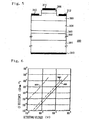
- Figure 6 shows the relation between a withstand voltage and an ON-state resistance obtained by simulation for the thyristor shown in Fig. 5.
- the line (1001) shows the relation for the thyristor formed of molybdenum oxide with a bandgap of 3.75 eV
- the line (1002) shows that for SiC device
- the line (1003) shows that for Si device.
- the results shown in Fig. 6 mean that a thyristor with much superior characteristics relative to those of thyristor formed of Si or SiC can be obtained using molybdenum oxide. That is, a thyristor with much superior characteristics than those of known thyristors without using an expensive substrate and fabrication process at a high temperature.
- a structure in which npnp-type conductive layers are included from the top layer on which the cathode electrode is formed to the bottom in illustrated in Fig. 5, a structure in which pnpn-type conductive layers are included from the top to the bottom is also allowable.
- a diode which includes one pn junction can be formed if a bipolar transistor which includes two pn junctions can be achieved. Therefore, a pn junction diode is also included in the scope of the present invention.
Landscapes
- Bipolar Transistors (AREA)
- Thyristors (AREA)
- Junction Field-Effect Transistors (AREA)
- Liquid Deposition Of Substances Of Which Semiconductor Devices Are Composed (AREA)
- Metal-Oxide And Bipolar Metal-Oxide Semiconductor Integrated Circuits (AREA)
Applications Claiming Priority (1)
| Application Number | Priority Date | Filing Date | Title |
|---|---|---|---|
| JP2005011248A JP5089020B2 (ja) | 2005-01-19 | 2005-01-19 | 基板上に作製された半導体電子デバイス |
Publications (2)
| Publication Number | Publication Date |
|---|---|
| EP1684355A2 true EP1684355A2 (de) | 2006-07-26 |
| EP1684355A3 EP1684355A3 (de) | 2009-03-18 |
Family
ID=36143331
Family Applications (1)
| Application Number | Title | Priority Date | Filing Date |
|---|---|---|---|
| EP06000614A Withdrawn EP1684355A3 (de) | 2005-01-19 | 2006-01-12 | Halbleiteranordnungen mit Molybdänoxid und Verfahren zur Herstellung |
Country Status (7)
| Country | Link |
|---|---|
| US (1) | US7557385B2 (de) |
| EP (1) | EP1684355A3 (de) |
| JP (1) | JP5089020B2 (de) |
| KR (2) | KR101240700B1 (de) |
| CN (1) | CN1828930A (de) |
| DE (1) | DE06000614T1 (de) |
| TW (1) | TWI413250B (de) |
Families Citing this family (11)
| Publication number | Priority date | Publication date | Assignee | Title |
|---|---|---|---|---|
| JP4519423B2 (ja) * | 2003-05-30 | 2010-08-04 | 創世理工株式会社 | 半導体を用いた光デバイス |
| JP4351869B2 (ja) * | 2003-06-10 | 2009-10-28 | 隆 河東田 | 半導体を用いた電子デバイス |
| JP4603370B2 (ja) * | 2005-01-18 | 2010-12-22 | 創世理工株式会社 | 基板上に作製された半導体光デバイスおよびその作製方法 |
| JP5214194B2 (ja) * | 2007-08-10 | 2013-06-19 | 住友化学株式会社 | 金属ドープモリブデン酸化物層を含む有機エレクトロルミネッセンス素子及び製造方法 |
| EP2674992A1 (de) | 2012-06-15 | 2013-12-18 | Imec | LED und Verfahren zur Herstellung einer LED |
| CN107946322A (zh) * | 2017-12-15 | 2018-04-20 | 京东方科技集团股份有限公司 | 阵列基板及其制造方法、显示装置 |
| US11374171B2 (en) | 2019-06-17 | 2022-06-28 | Samsung Electronics Co., Ltd. | Memristor and neuromorphic device comprising the same |
| KR102796867B1 (ko) | 2019-12-27 | 2025-04-17 | 삼성전자주식회사 | 가변 저항 메모리 소자 |
| KR102796866B1 (ko) | 2019-12-27 | 2025-04-17 | 삼성전자주식회사 | 가변 저항 메모리 소자 |
| US12113279B2 (en) | 2020-09-22 | 2024-10-08 | Oti Lumionics Inc. | Device incorporating an IR signal transmissive region |
| WO2022123431A1 (en) | 2020-12-07 | 2022-06-16 | Oti Lumionics Inc. | Patterning a conductive deposited layer using a nucleation inhibiting coating and an underlying metallic coating |
Citations (1)
| Publication number | Priority date | Publication date | Assignee | Title |
|---|---|---|---|---|
| EP1487022A2 (de) | 2003-06-10 | 2004-12-15 | Takashi Katoda | Elektronische Bauelemente aus hochreinem Molybdänoxid |
Family Cites Families (24)
| Publication number | Priority date | Publication date | Assignee | Title |
|---|---|---|---|---|
| FR972330A (fr) * | 1941-02-01 | 1951-01-29 | Redresseurs statiques de courant et leur procédé de fabrication | |
| JPS5128983B1 (de) | 1966-10-28 | 1976-08-23 | ||
| US3728594A (en) | 1971-11-17 | 1973-04-17 | Rca Corp | Electroluminescent device comprising a transition metal oxide doped with a trivalent rare earth element |
| JPS597719B2 (ja) | 1975-10-11 | 1984-02-20 | 田辺製薬株式会社 | シチジン誘導体の製法 |
| US4373145A (en) | 1979-06-18 | 1983-02-08 | Ford Motor Company | Thin film electroluminescent device |
| US4965594A (en) | 1986-02-28 | 1990-10-23 | Canon Kabushiki Kaisha | Liquid jet recording head with laminated heat resistive layers on a support member |
| JPH0663799B2 (ja) | 1987-10-05 | 1994-08-22 | 株式会社村田製作所 | 熱型流量検出装置 |
| US5401587A (en) | 1990-03-27 | 1995-03-28 | Kabushiki Kaisha Toyota Chuo Kenkyusho | Anisotropic nanophase composite material and method of producing same |
| EP0478799B1 (de) * | 1990-04-24 | 1996-12-04 | Ramtron International Corporation | Halbleiteranordnung mit ferroelektrischem material und verfahren zu deren herstellung |
| US5838029A (en) | 1994-08-22 | 1998-11-17 | Rohm Co., Ltd. | GaN-type light emitting device formed on a silicon substrate |
| US6202471B1 (en) | 1997-10-10 | 2001-03-20 | Nanomaterials Research Corporation | Low-cost multilaminate sensors |
| JP4183299B2 (ja) | 1998-03-25 | 2008-11-19 | 株式会社東芝 | 窒化ガリウム系化合物半導体発光素子 |
| EP1094294B1 (de) * | 1999-10-22 | 2002-12-04 | Brown & Sharpe Tesa S.A. | Vorrichtung zur Messung der Linear- oder Winkelverschiebung |
| JP2002055226A (ja) | 2000-08-07 | 2002-02-20 | Nippon Sheet Glass Co Ltd | 偏光素子及びその製造方法 |
| JP2002217425A (ja) | 2001-01-16 | 2002-08-02 | Sanken Electric Co Ltd | 半導体装置用電極、半導体装置及びその製造方法 |
| US6498358B1 (en) * | 2001-07-20 | 2002-12-24 | Motorola, Inc. | Structure and method for fabricating an electro-optic system having an electrochromic diffraction grating |
| SG142163A1 (en) | 2001-12-05 | 2008-05-28 | Semiconductor Energy Lab | Organic semiconductor element |
| US6627959B1 (en) | 2002-04-16 | 2003-09-30 | Boston Microsystems, Inc. | P-n junction sensor |
| JP4519423B2 (ja) * | 2003-05-30 | 2010-08-04 | 創世理工株式会社 | 半導体を用いた光デバイス |
| US7520790B2 (en) * | 2003-09-19 | 2009-04-21 | Semiconductor Energy Laboratory Co., Ltd. | Display device and manufacturing method of display device |
| US20050240501A1 (en) * | 2004-04-23 | 2005-10-27 | Liang-Jung Huang | Global financial commodity bull/bear positioning device |
| US7372070B2 (en) * | 2004-05-12 | 2008-05-13 | Matsushita Electric Industrial Co., Ltd. | Organic field effect transistor and method of manufacturing the same |
| US7378286B2 (en) * | 2004-08-20 | 2008-05-27 | Sharp Laboratories Of America, Inc. | Semiconductive metal oxide thin film ferroelectric memory transistor |
| JP4603370B2 (ja) | 2005-01-18 | 2010-12-22 | 創世理工株式会社 | 基板上に作製された半導体光デバイスおよびその作製方法 |
-
2005
- 2005-01-19 JP JP2005011248A patent/JP5089020B2/ja not_active Expired - Fee Related
-
2006
- 2006-01-12 EP EP06000614A patent/EP1684355A3/de not_active Withdrawn
- 2006-01-12 US US11/330,153 patent/US7557385B2/en not_active Expired - Fee Related
- 2006-01-12 DE DE06000614T patent/DE06000614T1/de active Pending
- 2006-01-13 TW TW095101470A patent/TWI413250B/zh not_active IP Right Cessation
- 2006-01-17 KR KR1020060004788A patent/KR101240700B1/ko not_active Expired - Fee Related
- 2006-01-18 CN CNA2006100049723A patent/CN1828930A/zh active Pending
-
2012
- 2012-12-24 KR KR1020120151998A patent/KR20130006584A/ko not_active Ceased
Patent Citations (1)
| Publication number | Priority date | Publication date | Assignee | Title |
|---|---|---|---|---|
| EP1487022A2 (de) | 2003-06-10 | 2004-12-15 | Takashi Katoda | Elektronische Bauelemente aus hochreinem Molybdänoxid |
Non-Patent Citations (3)
| Title |
|---|
| CROSS J S ET AL.: "Low pressure and inductive plasma enhanced chemical vapor deposition of [alpha]-MoO from Mo(CO)6 and 02 using experimental design", JOURNAL OF CHEMICAL VAPOR DEPOSITION USA, vol. 2, 1 July 1993 (1993-07-01), pages 59 - 78 |
| JULIEN C ET AL.: "JOURNAL OF CRYSTAL GROWTH", vol. 156, 1 November 1995, ELSEVIER, article "Synthesis and characterization of flash-evaporated Mo03 thin films", pages: 235 - 244 |
| JULIEN C ET AL: "Synthesis and characterization of flash-evaporated MoO3 thin films", JOURNAL OF CRYSTAL GROWTH, ELSEVIER, AMSTERDAM, NL, vol. 156, no. 3, 1 November 1995 (1995-11-01), pages 235 - 244, XP004000924, ISSN: 0022-0248, DOI: 10.1016/0022-0248(95)00269-3 * |
Also Published As
| Publication number | Publication date |
|---|---|
| EP1684355A3 (de) | 2009-03-18 |
| KR20130006584A (ko) | 2013-01-17 |
| CN1828930A (zh) | 2006-09-06 |
| US7557385B2 (en) | 2009-07-07 |
| JP2006202872A (ja) | 2006-08-03 |
| TW200701450A (en) | 2007-01-01 |
| US20060157695A1 (en) | 2006-07-20 |
| KR20060084366A (ko) | 2006-07-24 |
| TWI413250B (zh) | 2013-10-21 |
| JP5089020B2 (ja) | 2012-12-05 |
| DE06000614T1 (de) | 2007-01-18 |
| KR101240700B1 (ko) | 2013-03-18 |
Similar Documents
| Publication | Publication Date | Title |
|---|---|---|
| Zolper et al. | Advances in silicon carbide electronics | |
| Wright et al. | Prospects for SiC electronics and sensors | |
| KR20130006584A (ko) | 기판상에 형성된 전자 장치 및 그 제조 방법 | |
| Xiong et al. | Double-barrier β-Ga 2 O 3 Schottky barrier diode with low turn-on voltage and leakage current | |
| Singh | Reliability and performance limitations in SiC power devices | |
| JP5254037B2 (ja) | 高電圧炭化ケイ素半導体デバイスのための環境的に堅固なパッシベーション構造 | |
| JP7054853B2 (ja) | 炭化珪素半導体素子およびその製造方法 | |
| JP7819423B2 (ja) | 分極方向が変更可能な半導体デバイス | |
| EP3022772B1 (de) | Verbessertes gate-dielektrikum für ein feldeffektbauelement mit graben-gate | |
| KR20230131792A (ko) | 니켈-코발트 합금/산화갈륨 기반 전력 반도체 장치 및 그 제조 방법 | |
| US6900477B1 (en) | Processing technique to improve the turn-off gain of a silicon carbide gate turn-off thyristor and an article of manufacture | |
| US20070164312A1 (en) | Electronic devices formed of high-purity molybdenum oxide | |
| Than et al. | Vertical p-GaN/n-Ga 2 O 3 heterojunction diode with high switching performance | |
| Higashiwaki et al. | Depletion-mode Ga 2 O 3 MOSFETs | |
| Binari et al. | III-V nitride electronic devices | |
| Taube et al. | Electrical properties of isotype and anisotype ZnO/4H-SiC heterojunction diodes | |
| JP2013140981A (ja) | 窒化物系半導体素子及びその製造方法 | |
| CN119277804A (zh) | 一种增强型氮化物半导体晶体管结构 | |
| CN120264825A (zh) | 碳化硅场效应晶体管 | |
| Iwasaki et al. | Current enhancement by conductivity modulation in diamond JFETs for next generation low-loss power devices | |
| Igawa | Unleashing the potential of α-Ga2O3 | |
| HK1094738A (en) | Electronic devices formed on substrates and their fabrication methods | |
| Brandt et al. | SiC for applications in high-power electronics | |
| Singh | Silicon Carbide bipolar power devices-potentials and limits | |
| Higashiwaki et al. | Research and development on Ga 2 O 3 transistors and diodes |
Legal Events
| Date | Code | Title | Description |
|---|---|---|---|
| PUAI | Public reference made under article 153(3) epc to a published international application that has entered the european phase |
Free format text: ORIGINAL CODE: 0009012 |
|
| AK | Designated contracting states |
Kind code of ref document: A2 Designated state(s): AT BE BG CH CY CZ DE DK EE ES FI FR GB GR HU IE IS IT LI LT LU LV MC NL PL PT RO SE SI SK TR |
|
| AX | Request for extension of the european patent |
Extension state: AL BA HR MK YU |
|
| REG | Reference to a national code |
Ref country code: SE Ref legal event code: TRCL |
|
| EL | Fr: translation of claims filed | ||
| DET | De: translation of patent claims | ||
| PUAL | Search report despatched |
Free format text: ORIGINAL CODE: 0009013 |
|
| AK | Designated contracting states |
Kind code of ref document: A3 Designated state(s): AT BE BG CH CY CZ DE DK EE ES FI FR GB GR HU IE IS IT LI LT LU LV MC NL PL PT RO SE SI SK TR |
|
| AX | Request for extension of the european patent |
Extension state: AL BA HR MK YU |
|
| 17P | Request for examination filed |
Effective date: 20090618 |
|
| 17Q | First examination report despatched |
Effective date: 20090728 |
|
| AKX | Designation fees paid |
Designated state(s): DE FI FR GB IT SE |
|
| APBK | Appeal reference recorded |
Free format text: ORIGINAL CODE: EPIDOSNREFNE |
|
| APBN | Date of receipt of notice of appeal recorded |
Free format text: ORIGINAL CODE: EPIDOSNNOA2E |
|
| APBR | Date of receipt of statement of grounds of appeal recorded |
Free format text: ORIGINAL CODE: EPIDOSNNOA3E |
|
| APAV | Appeal reference deleted |
Free format text: ORIGINAL CODE: EPIDOSDREFNE |
|
| APBT | Appeal procedure closed |
Free format text: ORIGINAL CODE: EPIDOSNNOA9E |
|
| STAA | Information on the status of an ep patent application or granted ep patent |
Free format text: STATUS: THE APPLICATION IS DEEMED TO BE WITHDRAWN |
|
| 18D | Application deemed to be withdrawn |
Effective date: 20150801 |