EP1684345A2 - Surface mount semiconductor device - Google Patents
Surface mount semiconductor device Download PDFInfo
- Publication number
- EP1684345A2 EP1684345A2 EP06000841A EP06000841A EP1684345A2 EP 1684345 A2 EP1684345 A2 EP 1684345A2 EP 06000841 A EP06000841 A EP 06000841A EP 06000841 A EP06000841 A EP 06000841A EP 1684345 A2 EP1684345 A2 EP 1684345A2
- Authority
- EP
- European Patent Office
- Prior art keywords
- lead
- package
- semiconductor device
- surface mount
- leads
- Prior art date
- Legal status (The legal status is an assumption and is not a legal conclusion. Google has not performed a legal analysis and makes no representation as to the accuracy of the status listed.)
- Granted
Links
Images


Classifications
-
- H—ELECTRICITY
- H10—SEMICONDUCTOR DEVICES; ELECTRIC SOLID-STATE DEVICES NOT OTHERWISE PROVIDED FOR
- H10W—GENERIC PACKAGES, INTERCONNECTIONS, CONNECTORS OR OTHER CONSTRUCTIONAL DETAILS OF DEVICES COVERED BY CLASS H10
- H10W70/00—Package substrates; Interposers; Redistribution layers [RDL]
- H10W70/40—Leadframes
- H10W70/479—Leadframes on or in insulating or insulated package substrates, interposers, or redistribution layers
-
- H—ELECTRICITY
- H10—SEMICONDUCTOR DEVICES; ELECTRIC SOLID-STATE DEVICES NOT OTHERWISE PROVIDED FOR
- H10W—GENERIC PACKAGES, INTERCONNECTIONS, CONNECTORS OR OTHER CONSTRUCTIONAL DETAILS OF DEVICES COVERED BY CLASS H10
- H10W70/00—Package substrates; Interposers; Redistribution layers [RDL]
- H10W70/40—Leadframes
- H10W70/421—Shapes or dispositions
- H10W70/424—Cross-sectional shapes
- H10W70/427—Bent parts
-
- H—ELECTRICITY
- H10—SEMICONDUCTOR DEVICES; ELECTRIC SOLID-STATE DEVICES NOT OTHERWISE PROVIDED FOR
- H10W—GENERIC PACKAGES, INTERCONNECTIONS, CONNECTORS OR OTHER CONSTRUCTIONAL DETAILS OF DEVICES COVERED BY CLASS H10
- H10W74/00—Encapsulations, e.g. protective coatings
-
- H—ELECTRICITY
- H10—SEMICONDUCTOR DEVICES; ELECTRIC SOLID-STATE DEVICES NOT OTHERWISE PROVIDED FOR
- H10W—GENERIC PACKAGES, INTERCONNECTIONS, CONNECTORS OR OTHER CONSTRUCTIONAL DETAILS OF DEVICES COVERED BY CLASS H10
- H10W90/00—Package configurations
- H10W90/701—Package configurations characterised by the relative positions of pads or connectors relative to package parts
- H10W90/751—Package configurations characterised by the relative positions of pads or connectors relative to package parts of bond wires
- H10W90/756—Package configurations characterised by the relative positions of pads or connectors relative to package parts of bond wires between a chip and a stacked lead frame, conducting package substrate or heat sink
Definitions
- the present invention relates to a surface mount semiconductor device. More particularly, the present invention relates to a surface mount semiconductor device using a package formed by insert-molding a lead frame with a resin.
- Japanese Patent Laid-Open Publication No. 2003-007946 describes the following structure as a conventional technique.
- a lead frame for multiple devices is manufactured by pressing and stamping a metal board.
- the lead frame is then insert-molded with a resin so as to form a plurality of packages for surface mount semiconductor devices.
- Each package has a concave portion at its center.
- a semiconductor chip is mounted on the lead frame exposed at a bottom of the concave portion of each package and is sealed with a resin.
- the lead frame projecting laterally from a side face of each package is bent (i.e., a forming process) so as to extend around the package toward a rear surface of the package via the side face.
- Fig. 1 partially shows a part of the lead frame for multiple devices, which is used in the aforementioned surface mount semiconductor device.
- the shown part corresponds to one surface mount semiconductor device.
- the lead frame 100 includes a lead portion 101 on which a semiconductor chip is to be mounted (die-bonded) and a lead portion 102 to which one end of a bonding wire connected to the semiconductor chip at the other end thereof is connected (wire-bonded). Those two lead portions 101 and 102 are separated from each other.
- a package 103 is formed by insert molding with a resin on a die bonding pad 108 and a wire bonding pad 109 that are parts of the lead frame 100 at which die bonding and wire bonding are achieved, respectively.
- the lead portions 101 and 102 projecting laterally from a pair of opposed side faces 104 and 105 of the package 103 are bent along the side faces 104 and 105 and a rear face (not shown) of the package 103.
- Elongate through holes 106 and 107 are provided at centers of the lead portions 101 and 102, respectively.
- Each of the elongate through holes 106 and 107 has an approximately rectangular shape that is approximately perpendicular to a projecting direction of the corresponding lead portion 101 or 102 from the side face of the package 103 when the package 103 is formed.
- the lead portions 101 and 102 projecting from the package 103 can be bent approximately perpendicularly along the side faces 104 and 105 of the package 103 at positions of the elongate through holes 106 and 107, respectively.
- the reason for providing the elongate through holes 106 and 107 is that the elongate through holes 106 and 107 can reduce cross-sectional areas of bending portions of the lead portions 101 and 102, respectively, thereby enabling the forming process to be easily performed with a smaller load, as compared with a case in which the elongate through holes 106 and 107 are not provided.
- the lead portions 101 and 102 can be easily bent with a smaller load.
- the above reduction of the cross-sectional area makes a thermal resistance of each lead portion 101 or 102 larger. Therefore, a property for radiating the heat generated from the semiconductor chip is degraded, thus degrading the properties of the semiconductor chip.
- the lead portions 101 and 102 may be broken by vibration or impact after mounting. In this case, the semiconductor device is inoperative.
- the elongate through holes 106 and 107 are partially located in the package 103. Thus, when the elongate through holes 106 and 107 become larger, moisture absorption into the package 103 may proceed more so as to make the properties of the semiconductor chip poor.
- the present invention was made in view of the aforementioned problems. It is an object of the present invention to provide a surface mount semiconductor device using a lead frame, in which, assuming that a lead portion projecting from a package formed by insert-molding the lead frame with a resin is bent approximately perpendicularly along a side face of the package, the cross-sectional area of the lead at a center of a bending portion of the lead is reduced in advance, and which can prevent disconnection and ensure moisture resistance without impairing a heat radiation property.
- a surface mount semiconductor device In the surface mount semiconductor device, a lead frame is insert-molded to a package that is formed of a resin and has a concave potion. The concave portion is filled with a transparent resin to seal a semiconductor chip mounted at a bottom of the concave portion with the transparent resin. A pair of leads projecting laterally from side faces of the package that are opposed to each other are bent approximately perpendicularly along the side faces of the package at portions at which the leads project from the package.
- the surface mount semiconductor device further includes means for reducing a cross-sectional area of each of the leads that is partially provided at a center of the bending portion of the lead.
- the means for reducing the cross-sectional area of each of the leads may be formed by a concave elongate groove that does not penetrate through that lead in a thickness direction, is formed on at least one surface of the lead, and has an approximately V-shaped or U-shaped cross section when the bending portion of the lead is cut perpendicularly to the side face of the package from which the lead projects.
- the means for reducing the cross-sectional area of each of the leads may be formed by a plurality of concave grooves that do not penetrate through that lead in a thickness direction and are formed on at least one surface of the lead, each of the concave grooves having an approximately V-shaped or U-shaped cross section when the bending portion of the lead is cut parallel to the side face of the package from which that lead projects.
- a surface mount semiconductor device includes: a lead frame; a package that is formed of a resin and has a concave portion, the lead frame as an insert being insert-molded to the package; a semiconductor element mounted at the concave portion and electrically connected with the lead frame; and a resin sealing portion which seals the semiconductor element with a transparent resin.
- the lead frame may have a pair of leads extending laterally from side faces of the package that are opposed to each other, and the leads are bent along the side faces of the package. Furthermore, a portion of the lead which is bent may be reduced in cross-sectional thickness.
- the portion of the lead that is bent may be reduced in cross sectional thickness at its center partially.
- the portion of the lead that is bent may be provided with at least one groove to be reduced in cross-sectional thickness.
- a cross-sectional shape of the groove may be V-shaped or U-shaped.
- the groove may be provided in a direction perpendicular to a direction in which the lead extends.
- the groove may be provided parallel to a direction in which the lead extends.
- the groove may include an elongate groove which is provided in a direction perpendicular to a direction in which the lead extends and which is shorter than a width of the lead.
- the groove may include a plurality of short grooves which are provided parallel to a direction in which the lead extends to reduce a cross-sectional thickness of the lead.
- a package is formed by insert-molding a lead frame with a resin.
- a pair of leads projecting laterally from side faces of the package that are opposed to each other are bent approximately perpendicularly along the side faces of the package at portions at which the leads project from the package.
- the cross-sectional area of each lead is partially reduced at a center of the bending portion of that lead.
- the present invention has the following advantages; It is possible to suppress stress applied to the package near the bending portions of the respective leads when the leads are bent; It is also possible to prevent occurrence of troubles such as degradation of adhesiveness between the package and the leads and breakage of the package, caused by a heat generated in soldering in a mounting process, a heat generated from an operating semiconductor chip, or the like. Therefore, it is possible to prevent electric properties from becoming poor because of poor moisture resistance caused by the above troubles.
- Fig. 2 shows a lead frame 1 for multiple devices, which is used for a surface mount semiconductor device according to the present exemplary embodiment.
- the lead frame 1 can be formed by pressing and stamping or etching a metal plate to remove an unnecessary portion of the metal plate.
- the metal plate can be formed by a Cu alloy plate plated with Ni, Pd, Au, Ag, or the like.
- a plurality of the same lead patterns 2 that are independent of each other can be arranged in one line at predetermined intervals in the lead frame 1 for multiple devices.
- Each of the lead patterns 2 can form an individual surface mount semiconductor device.
- a plurality of feed holes 3 can be provided at both ends of the lead frame 1 along a longitudinal direction of the lead frame 1 so as to be arranged at predetermined intervals on straight lines parallel to each other.
- the lead pattern 2 can include a pair of leads that are separated from each other.
- One lead 5 can have a die bonding pad 4 to which a semiconductor chip is die-bonded.
- the other lead 7 can have a wire bonding pad 6 to which one end of a bonding wire connected to an upper electrode of the die-bonded semiconductor chip at the other end is connected.
- One through hole 8 may be provided in the lead 5 and two through holes 9 may be provided in the lead 7.
- Parts of a package that is formed by insert-molding the lead frame 1 with a resin so as to cover the leads 5 and 7 from both sides are connected to each other via the through holes 8 and 9 in the leads 5 and 7, so that the leads 5 and 7 and the package covering those leads 5 and 7 from both sides are fixed and integrated as one unit.
- a concave portion 10 is provided in each of the leads 5 and 7.
- the concave portion 10 is arranged outside the through hole 8 or the through holes 9 at the center of each lead 5 or 7.
- the position of the concave portion 10 corresponds to a base of the package formed by insert molding with a resin.
- the concave portions 10 correspond to bending portions at which the leads 5 and 7 projecting laterally from side faces of the package are bent approximately perpendicularly along the side faces of the package in a forming process.
- the concave portions 10 are provided in order to reduce cross-sectional areas of the bending portions of the leads 5 and 7, thereby enabling the leads 5 and 7 to be easily bent with a smaller load.
- the concave portion 10 formed in each of the leads 5 and 7 can have various structures. Basically, the concave portions 10 are formed to extend parallel to the side faces of the package from which the leads 5 and 7 project in such a manner that the concave portions 10 do not penetrate through the leads 5 and 7, respectively. Moreover, no concave portion is formed on at least a part of a straight line on which the concave portion 10 is provided, so that the thickness of the lead 5 or 7 can be maintained at that part without change.
- Figs. 3 to 6 show exemplary shapes of the concave portion 10 in Figs. 3 to 6.
- Fig. 3 shows a cross section taken along the line A-A and the line B-B in Fig. 2 and shows a first exemplary shape of the concave portion 10.
- Fig. 4 also shows a cross section taken along the line A-A and line B-B in Fig. 2 and shows a second exemplary shape of the concave portion 10.
- Fig. 5 shows a cross section taken along the line C-C and the line D-D in Fig. 2 and shows a third exemplary shape of the concave portion 10.
- Fig. 5 also shows a cross section taken along the line C-C and the line D-D in Fig. 2 and shows a fourth exemplary shape of the concave portion.
- the first exemplary shape of the concave portion 10 is formed by an elongate groove having an approximately V-shaped cross section when the concave portion 10 is cut along the direction in which the lead extends.
- the second exemplary shape of the concave portion 10 is formed by an elongate groove having an approximately U-shaped cross section when the concave portion 10 is cut along the direction in which the lead extends.
- the third exemplary shape of the concave portion 10 is formed by a plurality of approximately V-shaped independent grooves that are arranged on an approximately straight line, when the concave portion 10 is cut along the direction perpendicular to the direction in which the lead extends (the widthwise direction of the lead).
- the fourth exemplary shape of the concave portion 10 is formed by a plurality of approximately U-shaped independent grooves that are arranged on an approximately straight line, when the concave portion 10 is cut along the direction perpendicular to the direction in which the lead extends.
- a depth of the groove having the approximately V-shaped cross section and that of the groove having the approximately U-shaped cross section be within a range from 1/5 to 2/3 of the thickness of the lead frame.
- the cross-sectional area of the lead at the concave portion is smaller than that at any other portions of the lead where no concave portion is provided. Therefore, when the lead is bent at the concave portion, it is possible to easily bend the lead with a smaller load.
- Figs. 7 and 8 show a state in which a package 11 is formed by insert-molding the aforementioned lead frame 1 with a resin.
- Fig. 7 is a plan view and Fig. 8 shows a cross section taken along the line E-E in Fig. 7.
- a concave portion 12 is formed at a center of the package 11.
- the die bonding pad 4 and the wire bonding pad 6 of the leads 5 and 7 are exposed at a bottom of the concave portion 12.
- the lead portions 5 and 7 laterally project from side faces of the package 11, respectively.
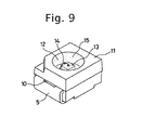
- Fig. 9 shows a surface mount semiconductor device having been completed in the following manner;
- the individual packages 11 are formed on the lead frame 1 for multiple devices;
- the die bonding pad and the wire bonding pad are exposed at the bottom of the concave portion 12 of each package 11 and a semiconductor chip 13 is die-bonded to each die bonding pad and a bonding wire 14 is wire-bonded to each wire bonding pad;
- the concave portion 12 is filled with a transparent resin 15 to seal the semiconductor chip 13 and the bonding wire 14 with the transparent resin 15;
- the lead portions 5 and 7 projecting from the side faces of the package 11 are bent approximately perpendicularly along the side faces of the package 11 at the positions at which the leads 5 and 7 project from the package, and are further bent approximately perpendicularly along the bottom of the package.
- the individual semiconductor devices are separated from each other.
- the cross-sectional area of each of the leads 5 and 7 projecting laterally from the side faces of the package 11 can be reduced by providing the concave portions 10 at the positions at which the leads project from the package 11 and are bent approximately perpendicularly along the side face of the package 11 so as not to penetrate through the leads 5 and 7 in a thickness direction, respectively.
- the leads 5 and 7 can be easily bent with a smaller bending load.
- the concave portion is preferably provided at the center of each lead while the thickness of that lead is maintained at a portion other than the concave portion.
- Reduction of the cross-sectional area of the lead makes a thermal resistance larger and therefore degrades a property for radiating a heat generated from a semiconductor chip. This degrades the properties of the semiconductor chip.
- a reduction rate of the cross-sectional area is smaller and the thermal resistance is relatively smaller, as compared with a conventional method for providing an elongate through hole.
- the degree of degradation of the properties of the semiconductor chip caused by degradation of the heat radiation property is low and is less of an obstacle in use.
- the concave portion 10 is provided on the surface of the lead, that is opposite to the bending direction of the lead.
- the concave portion may be provided on a surface of the lead on the same side as the bending direction of the lead or on both surfaces of the lead.
Landscapes
- Lead Frames For Integrated Circuits (AREA)
- Structures Or Materials For Encapsulating Or Coating Semiconductor Devices Or Solid State Devices (AREA)
- Encapsulation Of And Coatings For Semiconductor Or Solid State Devices (AREA)
- Led Device Packages (AREA)
Abstract
Description
- The present invention relates to a surface mount semiconductor device. More particularly, the present invention relates to a surface mount semiconductor device using a package formed by insert-molding a lead frame with a resin.
- Various structures for a surface mount semiconductor device are known. For example, Japanese Patent Laid-Open Publication No. 2003-007946 describes the following structure as a conventional technique. A lead frame for multiple devices is manufactured by pressing and stamping a metal board. The lead frame is then insert-molded with a resin so as to form a plurality of packages for surface mount semiconductor devices. Each package has a concave portion at its center. Then, a semiconductor chip is mounted on the lead frame exposed at a bottom of the concave portion of each package and is sealed with a resin. Finally, the lead frame projecting laterally from a side face of each package is bent (i.e., a forming process) so as to extend around the package toward a rear surface of the package via the side face.
- Fig. 1 partially shows a part of the lead frame for multiple devices, which is used in the aforementioned surface mount semiconductor device. The shown part corresponds to one surface mount semiconductor device. The
lead frame 100 includes alead portion 101 on which a semiconductor chip is to be mounted (die-bonded) and alead portion 102 to which one end of a bonding wire connected to the semiconductor chip at the other end thereof is connected (wire-bonded). Those twolead portions - A
package 103 is formed by insert molding with a resin on adie bonding pad 108 and awire bonding pad 109 that are parts of thelead frame 100 at which die bonding and wire bonding are achieved, respectively. Thelead portions opposed side faces package 103 are bent along theside faces package 103. - Elongate through
holes lead portions holes corresponding lead portion package 103 when thepackage 103 is formed. Thelead portions package 103 can be bent approximately perpendicularly along theside faces package 103 at positions of the elongate throughholes holes holes lead portions holes - Accordingly, it is possible to suppress stress that is applied to the
package 103 near positions from which thelead portions lead portions package 103 is formed. It is also possible to prevent occurrence of troubles such as degradation of adhesiveness between thepackage 103 and thelead portions package 103, caused by a heat generated in soldering in a mounting process, a heat generated from the semiconductor chip that is operating, or the like. Therefore, it is possible to prevent the electric property from becoming poor because of poor moisture resistance caused by the above troubles. - As the length of the elongate through
holes lead portions package 103 and are bent becomes closer to the width of thelead portions lead portions lead portions - However, the above reduction of the cross-sectional area makes a thermal resistance of each
lead portion lead portions holes package 103. Thus, when the elongate throughholes package 103 may proceed more so as to make the properties of the semiconductor chip poor. - The present invention was made in view of the aforementioned problems. It is an object of the present invention to provide a surface mount semiconductor device using a lead frame, in which, assuming that a lead portion projecting from a package formed by insert-molding the lead frame with a resin is bent approximately perpendicularly along a side face of the package, the cross-sectional area of the lead at a center of a bending portion of the lead is reduced in advance, and which can prevent disconnection and ensure moisture resistance without impairing a heat radiation property.
- One of aspects of the invention is a surface mount semiconductor device. In the surface mount semiconductor device, a lead frame is insert-molded to a package that is formed of a resin and has a concave potion. The concave portion is filled with a transparent resin to seal a semiconductor chip mounted at a bottom of the concave portion with the transparent resin. A pair of leads projecting laterally from side faces of the package that are opposed to each other are bent approximately perpendicularly along the side faces of the package at portions at which the leads project from the package. In this configuration, the surface mount semiconductor device further includes means for reducing a cross-sectional area of each of the leads that is partially provided at a center of the bending portion of the lead.
- In the surface mount semiconductor device of the above configuration, the means for reducing the cross-sectional area of each of the leads may be formed by a concave elongate groove that does not penetrate through that lead in a thickness direction, is formed on at least one surface of the lead, and has an approximately V-shaped or U-shaped cross section when the bending portion of the lead is cut perpendicularly to the side face of the package from which the lead projects.
- In the surface mount semiconductor device of the above configuration, the means for reducing the cross-sectional area of each of the leads may be formed by a plurality of concave grooves that do not penetrate through that lead in a thickness direction and are formed on at least one surface of the lead, each of the concave grooves having an approximately V-shaped or U-shaped cross section when the bending portion of the lead is cut parallel to the side face of the package from which that lead projects.
- Another aspect of the invention is a surface mount semiconductor device includes: a lead frame; a package that is formed of a resin and has a concave portion, the lead frame as an insert being insert-molded to the package; a semiconductor element mounted at the concave portion and electrically connected with the lead frame; and a resin sealing portion which seals the semiconductor element with a transparent resin. In this configuration, the lead frame may have a pair of leads extending laterally from side faces of the package that are opposed to each other, and the leads are bent along the side faces of the package. Furthermore, a portion of the lead which is bent may be reduced in cross-sectional thickness.
- In the surface mount semiconductor device described above, the portion of the lead that is bent may be reduced in cross sectional thickness at its center partially.
- In the surface mount semiconductor device described above, the portion of the lead that is bent may be provided with at least one groove to be reduced in cross-sectional thickness.
- In the surface mount semiconductor device described above, a cross-sectional shape of the groove may be V-shaped or U-shaped.
- In the surface mount semiconductor device described above, the groove may be provided in a direction perpendicular to a direction in which the lead extends.
- In the surface mount semiconductor device described above, the groove may be provided parallel to a direction in which the lead extends.
- In the surface mount semiconductor device described above, the groove may include an elongate groove which is provided in a direction perpendicular to a direction in which the lead extends and which is shorter than a width of the lead.
- In the surface mount semiconductor device described above, the groove may include a plurality of short grooves which are provided parallel to a direction in which the lead extends to reduce a cross-sectional thickness of the lead.
- According to the present invention, a package is formed by insert-molding a lead frame with a resin. A pair of leads projecting laterally from side faces of the package that are opposed to each other are bent approximately perpendicularly along the side faces of the package at portions at which the leads project from the package. The cross-sectional area of each lead is partially reduced at a center of the bending portion of that lead.
- Thus, the present invention has the following advantages; It is possible to suppress stress applied to the package near the bending portions of the respective leads when the leads are bent; It is also possible to prevent occurrence of troubles such as degradation of adhesiveness between the package and the leads and breakage of the package, caused by a heat generated in soldering in a mounting process, a heat generated from an operating semiconductor chip, or the like. Therefore, it is possible to prevent electric properties from becoming poor because of poor moisture resistance caused by the above troubles.
- These and other objects and advantages of the invention will become clear from the following description with reference to the accompanying drawings, wherein:
- Fig. 1 is a plan view of a lead frame used in a conventional surface mount semiconductor device;
- Fig. 2 is a plan view of a lead frame used in an exemplary embodiment of a surface mount semiconductor device according to the present invention;
- Fig. 3 is a cross-section view taken along the line A-A and the line B-B in Fig. 2;
- Fig. 4 is a cross-section view taken along the line A-A and the line B-B in Fig. 2;
- Fig. 5 is a cross-section view taken along the line C-C and the line D-D in Fig. 2;
- Fig. 6 is a cross-section view taken along the line C-C and the line D-D in Fig. 2;
- Fig. 7 is a plan view of the lead frame used in the exemplary embodiment of the surface mount device according to the present invention, after the lead frame is insert-molded with a resin;
- Fig. 8 is a cross-sectional view taken along the line E-E in Fig. 7.
- Fig. 9 is a perspective view showing an exemplary embodiment of the surface mount device according to the present invention.
- A preferred exemplary embodiment of the present invention will now be described in detail, with reference to Figs. 2 to 9 (the same components are labeled with the same reference numerals). The exemplary embodiment described below has various limitations that are technically preferable, because that exemplary embodiment is a preferable specific example of the present invention. However, the scope of the present invention is not limited by that exemplary embodiment, unless the description for limiting the present invention is made.
- Fig. 2 shows a lead frame 1 for multiple devices, which is used for a surface mount semiconductor device according to the present exemplary embodiment. For example, the lead frame 1 can be formed by pressing and stamping or etching a metal plate to remove an unnecessary portion of the metal plate. Here, the metal plate can be formed by a Cu alloy plate plated with Ni, Pd, Au, Ag, or the like.
- A plurality of the
same lead patterns 2 that are independent of each other can be arranged in one line at predetermined intervals in the lead frame 1 for multiple devices. Each of thelead patterns 2 can form an individual surface mount semiconductor device. Alternatively, there may be two lines of thelead patterns 2 in the lead frame 1. A plurality offeed holes 3 can be provided at both ends of the lead frame 1 along a longitudinal direction of the lead frame 1 so as to be arranged at predetermined intervals on straight lines parallel to each other. - The
lead pattern 2 can include a pair of leads that are separated from each other. Onelead 5 can have adie bonding pad 4 to which a semiconductor chip is die-bonded. Theother lead 7 can have awire bonding pad 6 to which one end of a bonding wire connected to an upper electrode of the die-bonded semiconductor chip at the other end is connected. - One through
hole 8 may be provided in thelead 5 and two throughholes 9 may be provided in thelead 7. Parts of a package that is formed by insert-molding the lead frame 1 with a resin so as to cover theleads holes leads leads leads - Moreover, a
concave portion 10 is provided in each of theleads concave portion 10 is arranged outside the throughhole 8 or the throughholes 9 at the center of each lead 5 or 7. The position of theconcave portion 10 corresponds to a base of the package formed by insert molding with a resin. Theconcave portions 10 correspond to bending portions at which theleads concave portions 10 are provided in order to reduce cross-sectional areas of the bending portions of theleads leads - The
concave portion 10 formed in each of theleads concave portions 10 are formed to extend parallel to the side faces of the package from which theleads concave portions 10 do not penetrate through theleads concave portion 10 is provided, so that the thickness of thelead - The exemplary shapes of the
concave portion 10 are shown in Figs. 3 to 6. Fig. 3 shows a cross section taken along the line A-A and the line B-B in Fig. 2 and shows a first exemplary shape of theconcave portion 10. Fig. 4 also shows a cross section taken along the line A-A and line B-B in Fig. 2 and shows a second exemplary shape of theconcave portion 10. Fig. 5 shows a cross section taken along the line C-C and the line D-D in Fig. 2 and shows a third exemplary shape of theconcave portion 10. Fig. 5 also shows a cross section taken along the line C-C and the line D-D in Fig. 2 and shows a fourth exemplary shape of the concave portion. - The first exemplary shape of the
concave portion 10 is formed by an elongate groove having an approximately V-shaped cross section when theconcave portion 10 is cut along the direction in which the lead extends. The second exemplary shape of theconcave portion 10 is formed by an elongate groove having an approximately U-shaped cross section when theconcave portion 10 is cut along the direction in which the lead extends. The third exemplary shape of theconcave portion 10 is formed by a plurality of approximately V-shaped independent grooves that are arranged on an approximately straight line, when theconcave portion 10 is cut along the direction perpendicular to the direction in which the lead extends (the widthwise direction of the lead). The fourth exemplary shape of theconcave portion 10 is formed by a plurality of approximately U-shaped independent grooves that are arranged on an approximately straight line, when theconcave portion 10 is cut along the direction perpendicular to the direction in which the lead extends. - It is desirable that a depth of the groove having the approximately V-shaped cross section and that of the groove having the approximately U-shaped cross section be within a range from 1/5 to 2/3 of the thickness of the lead frame.
- In any of the above four exemplary shapes of the concave portion, the cross-sectional area of the lead at the concave portion is smaller than that at any other portions of the lead where no concave portion is provided. Therefore, when the lead is bent at the concave portion, it is possible to easily bend the lead with a smaller load.
- Figs. 7 and 8 show a state in which a
package 11 is formed by insert-molding the aforementioned lead frame 1 with a resin. Fig. 7 is a plan view and Fig. 8 shows a cross section taken along the line E-E in Fig. 7. Aconcave portion 12 is formed at a center of thepackage 11. Thedie bonding pad 4 and thewire bonding pad 6 of theleads concave portion 12. Thelead portions package 11, respectively. - Fig. 9 shows a surface mount semiconductor device having been completed in the following manner; The
individual packages 11 are formed on the lead frame 1 for multiple devices; The die bonding pad and the wire bonding pad are exposed at the bottom of theconcave portion 12 of eachpackage 11 and asemiconductor chip 13 is die-bonded to each die bonding pad and abonding wire 14 is wire-bonded to each wire bonding pad; Then, theconcave portion 12 is filled with atransparent resin 15 to seal thesemiconductor chip 13 and thebonding wire 14 with thetransparent resin 15; Thelead portions package 11 are bent approximately perpendicularly along the side faces of thepackage 11 at the positions at which theleads - As is apparent from Fig. 9, the cross-sectional area of each of the
leads package 11 can be reduced by providing theconcave portions 10 at the positions at which the leads project from thepackage 11 and are bent approximately perpendicularly along the side face of thepackage 11 so as not to penetrate through theleads leads - As a result, stress applied to the package near the position from which the leads project when the leads are bent can be suppressed. It is also possible to prevent occurrence of troubles such as degradation of adhesion between the package and the leads and breakage of the package, caused by a heat generated in soldering in the mounting process, a heat generated from the semiconductor chip that is operating, or the like. Therefore, it is possible to prevent electric properties from becoming poor because of poor moisture resistance caused by the above troubles.
- Moreover, instead of providing the concave portion across the full width of each lead, according to the present invention the concave portion is preferably provided at the center of each lead while the thickness of that lead is maintained at a portion other than the concave portion. Thus, even if external stress such as vibration or impact is applied to the surface mount semiconductor device of the present invention after the surface mount semiconductor device is mounted, disconnection can be prevented because of protection by the thicker portion of the lead, and a function of the device can be maintained.
- Reduction of the cross-sectional area of the lead makes a thermal resistance larger and therefore degrades a property for radiating a heat generated from a semiconductor chip. This degrades the properties of the semiconductor chip. However, a reduction rate of the cross-sectional area is smaller and the thermal resistance is relatively smaller, as compared with a conventional method for providing an elongate through hole. Thus, the degree of degradation of the properties of the semiconductor chip caused by degradation of the heat radiation property is low and is less of an obstacle in use.
- In the above exemplary embodiment, the
concave portion 10 is provided on the surface of the lead, that is opposite to the bending direction of the lead. Alternatively, the concave portion may be provided on a surface of the lead on the same side as the bending direction of the lead or on both surfaces of the lead.
Claims (11)
- A surface mount semiconductor device in which a lead frame (1) is insert-molded to a package that is formed of a resin and has a concave potion (12), the concave portion (12) is filled with a transparent resin to seal a semiconductor chip (13) mounted at a bottom of the concave portion (12) with the transparent resin, and a pair of leads (5, 7) projecting laterally from side faces of the package that are opposed to each other are bent approximately perpendicularly along the side faces of the package at portions at which the leads (5, 7) project from the package, the surface mount semiconductor device being characterized by including means (10) for reducing a cross-sectional area of each of the leads (5, 7) that is partially provided at a center of the bending portion of the lead (5, 7).
- The surface mount semiconductor device according to claim 1, characterized in that the means (10) for reducing the cross-sectional area of each of the leads (5, 7) is formed by a concave elongate groove (10) that does not penetrate through that lead (5, 7) in a thickness direction, is formed on at least one surface of the lead (5, 7), and has an approximately V-shaped or U-shaped cross section when the bending portion of the lead (5, 7) is cut perpendicularly to the side face of the package from which the lead (5, 7) projects.
- The surface mount semiconductor device according to claim 1, characterized in that the means (10) for reducing the cross-sectional area of each of the leads (5, 7) is formed by a plurality of concave grooves that do not penetrate through that lead (5, 7) in a thickness direction and are formed on at least one surface of the lead (5, 7), each of the concave grooves having an approximately V-shaped or U-shaped cross section when the bending portion of the lead (5, 7) is cut parallel to the side face of the package from which that lead (5, 7) projects.
- A surface mount semiconductor device comprising:a lead frame (1);a package that is formed of a resin and has a concave portion (12), the lead frame (1) as an insert being insert-molded to the package;a semiconductor element (13) mounted at the concave portion (12) and electrically connected with the lead frame (1); anda resin sealing portion which seals the semiconductor element (13) with a transparent resin,the surface mount semiconductor device beingcharacterized in that:the lead frame (1) has a pair of leads (5, 7) extending laterally from side faces of the package that are opposed to each other, the leads (5, 7) being bent along the side faces of the package; anda portion (10) of the lead (5, 7) which is bent is reduced in cross-sectional thickness.
- The surface mount semiconductor device according to claim 4, characterized in that the portion (10) of the lead (5, 7) that is bent is reduced in cross sectional thickness at its center partially.
- The surface mount semiconductor device according to claim 4, characterized in that the portion (10) of the lead (5, 7) that is bent is provided with at least one groove to be reduced in cross-sectional thickness.
- The surface mount semiconductor device according to claim 6, characterized in that a cross-sectional shape of the groove is V-shaped or U-shaped.
- The surface mount semiconductor device according to claim 6, characterized in that the groove is provided in a direction perpendicular to a direction in which the lead (5, 7) extends.
- The surface mount semiconductor device according to claim 6, characterized in that the groove is provided parallel to a direction in which the lead (5, 7) extends.
- The surface mount semiconductor device according to claim 6, characterized in that the groove comprises an elongate groove which is provided in a direction perpendicular to a direction in which the lead (5, 7) extends and which is shorter than a width of the lead (5, 7).
- The surface mount semiconductor device according to claim 6, characterized in that the groove comprises a plurality of short grooves which are provided parallel to a direction in which the lead (5, 7) extends to reduce a cross-sectional thickness of the lead (5, 7).
Applications Claiming Priority (1)
| Application Number | Priority Date | Filing Date | Title |
|---|---|---|---|
| JP2005014204A JP4698234B2 (en) | 2005-01-21 | 2005-01-21 | Surface mount semiconductor device |
Publications (3)
| Publication Number | Publication Date |
|---|---|
| EP1684345A2 true EP1684345A2 (en) | 2006-07-26 |
| EP1684345A3 EP1684345A3 (en) | 2008-04-02 |
| EP1684345B1 EP1684345B1 (en) | 2013-09-25 |
Family
ID=36282703
Family Applications (1)
| Application Number | Title | Priority Date | Filing Date |
|---|---|---|---|
| EP06000841.4A Expired - Lifetime EP1684345B1 (en) | 2005-01-21 | 2006-01-16 | Surface mount semiconductor device |
Country Status (4)
| Country | Link |
|---|---|
| US (1) | US7595549B2 (en) |
| EP (1) | EP1684345B1 (en) |
| JP (1) | JP4698234B2 (en) |
| CN (1) | CN1812085A (en) |
Families Citing this family (21)
| Publication number | Priority date | Publication date | Assignee | Title |
|---|---|---|---|---|
| JP2008198807A (en) * | 2007-02-14 | 2008-08-28 | Nichia Corp | Semiconductor device |
| TW200847478A (en) * | 2007-05-30 | 2008-12-01 | I Chiun Precision Ind Co Ltd | Light-emitting diode lead frame and manufacture method thereof |
| JP5180690B2 (en) * | 2008-06-06 | 2013-04-10 | アピックヤマダ株式会社 | LED chip mounting substrate manufacturing method, LED chip mounting substrate mold, LED chip mounting substrate, and LED |
| US8089075B2 (en) * | 2009-04-17 | 2012-01-03 | Avago Technologies Ecbu Ip (Singapore) Pte. Ltd. | LFCC package with a reflector cup surrounded by a single encapsulant |
| US8101955B2 (en) * | 2009-04-17 | 2012-01-24 | Avago Technologies Ecbu Ip (Singapore) Pte. Ltd. | PLCC package with a reflector cup surrounded by an encapsulant |
| USD624884S1 (en) * | 2009-10-26 | 2010-10-05 | Foxsemicon Integrated Technology, Inc. | Light emitting diode |
| USD622232S1 (en) * | 2009-10-26 | 2010-08-24 | Foxsemicon Integrated Technology, Inc. | Light emitting diode |
| USD627313S1 (en) * | 2010-02-01 | 2010-11-16 | Foxsemicon Integrated Technology, Inc. | Light-emitting diode |
| USD627314S1 (en) * | 2010-02-01 | 2010-11-16 | Foxsemicon Integrated Technology, Inc. | Light-emitting diode |
| USD627312S1 (en) * | 2010-02-01 | 2010-11-16 | Foxsemicon Integrated Technology, Inc. | Light-emitting diode |
| USD627311S1 (en) * | 2010-02-01 | 2010-11-16 | Foxsemicon Integrated Technology, Inc. | Light-emitting diode |
| USD651183S1 (en) * | 2010-02-01 | 2011-12-27 | Foxsemicon Integrated Technology, Inc. | Light-emitting diode |
| KR101141323B1 (en) * | 2010-12-24 | 2012-05-03 | 엘지이노텍 주식회사 | Light emitting element package |
| JP2013069903A (en) * | 2011-09-22 | 2013-04-18 | Fusheng Industrial Co Ltd | Light emission diode support frame construction, and manufacturing method thereof (1) |
| JP5885493B2 (en) * | 2011-12-21 | 2016-03-15 | 住友化学株式会社 | Semiconductor package and semiconductor light emitting device |
| USD759603S1 (en) * | 2013-07-17 | 2016-06-21 | Nuflare Technology, Inc. | Chamber of charged particle beam drawing apparatus |
| CN103855275A (en) * | 2013-12-25 | 2014-06-11 | 深圳市瑞丰光电子股份有限公司 | LED packaging support module, LED packaging support single body and LED packaging structure |
| JP6717079B2 (en) * | 2016-06-29 | 2020-07-01 | 日亜化学工業株式会社 | Light emitting device, manufacturing method thereof, and manufacturing method of package |
| JP6508276B2 (en) * | 2016-09-28 | 2019-05-08 | 日亜化学工業株式会社 | Light emitting device and method of manufacturing the same |
| US10243107B2 (en) * | 2016-09-28 | 2019-03-26 | Nichia Corporation | Light emitting device and method for manufacturing thereof |
| NL2026503B1 (en) * | 2020-09-18 | 2022-05-23 | Ampleon Netherlands Bv | Molded RF power package |
Citations (2)
| Publication number | Priority date | Publication date | Assignee | Title |
|---|---|---|---|---|
| JPS58215061A (en) | 1982-06-09 | 1983-12-14 | Hitachi Ltd | Semiconductor device and manufacture thereof |
| US20020185650A1 (en) | 2001-05-15 | 2002-12-12 | Yasushi Hasegawa | Photocoupler, method for fabricating the same and photocoupler fabrication apparatus |
Family Cites Families (32)
| Publication number | Priority date | Publication date | Assignee | Title |
|---|---|---|---|---|
| JPS60254646A (en) * | 1984-05-30 | 1985-12-16 | Fujitsu Ltd | Semiconductor device |
| JPH0214555A (en) * | 1989-05-19 | 1990-01-18 | Hitachi Ltd | Resin-sealed type semiconductor device |
| DE58909888C5 (en) | 1989-05-31 | 2017-03-02 | Osram Gesellschaft mit beschränkter Haftung | A method of manufacturing a surface mount opto-device and surface mount opto-device |
| JPH05267521A (en) * | 1992-03-19 | 1993-10-15 | Rohm Co Ltd | Structure of lead frame |
| JPH05267520A (en) * | 1992-03-19 | 1993-10-15 | Rohm Co Ltd | Shaping method of lead frame |
| JP3319828B2 (en) * | 1993-09-20 | 2002-09-03 | 株式会社日立製作所 | Bending method of high-rigid structure provided with reinforcing ribs and molding die |
| JPH088375A (en) * | 1994-06-23 | 1996-01-12 | Hitachi Ltd | Semiconductor device and lead frame and mold used for manufacturing the same |
| JP3417079B2 (en) * | 1994-08-31 | 2003-06-16 | ソニー株式会社 | Method for manufacturing semiconductor device |
| JPH08288448A (en) * | 1995-04-13 | 1996-11-01 | Dainippon Printing Co Ltd | Lead frame and resin-sealed semiconductor device |
| JP2842355B2 (en) * | 1996-02-01 | 1999-01-06 | 日本電気株式会社 | package |
| US6277225B1 (en) * | 1996-03-13 | 2001-08-21 | Micron Technology, Inc. | Stress reduction feature for LOC lead frame |
| EP1089335A4 (en) * | 1998-05-20 | 2002-02-06 | Rohm Co Ltd | SEMICONDUCTOR DEVICE |
| JP2000294711A (en) * | 1999-04-06 | 2000-10-20 | Sony Corp | Lead frame |
| JP2001168398A (en) * | 1999-12-13 | 2001-06-22 | Nichia Chem Ind Ltd | Light emitting diode and manufacturing method |
| DE10102119C1 (en) * | 2001-01-18 | 2002-04-04 | Vishay Semiconductor Gmbh | Optoelectronic component has electromagnetic screening provided by conductor strip region projecting from component housing and wrapped around outside of latter |
| US6940704B2 (en) * | 2001-01-24 | 2005-09-06 | Gelcore, Llc | Semiconductor light emitting device |
| JP4066608B2 (en) * | 2001-03-16 | 2008-03-26 | 日亜化学工業株式会社 | Package molded body and manufacturing method thereof |
| DE10117889A1 (en) * | 2001-04-10 | 2002-10-24 | Osram Opto Semiconductors Gmbh | Leadframe used for a light emitting diode component comprises a chip assembly region, a wire connecting region, external electrical connecting strips, and a support part coupled with a thermal connecting part |
| JP2002374007A (en) * | 2001-06-15 | 2002-12-26 | Toyoda Gosei Co Ltd | Light emitting device |
| JP2003007946A (en) * | 2001-06-27 | 2003-01-10 | Enomoto Co Ltd | Lead frame for surface mount type LED and method of manufacturing the same |
| JP4009097B2 (en) * | 2001-12-07 | 2007-11-14 | 日立電線株式会社 | LIGHT EMITTING DEVICE, ITS MANUFACTURING METHOD, AND LEAD FRAME USED FOR MANUFACTURING LIGHT EMITTING DEVICE |
| JP4211359B2 (en) * | 2002-03-06 | 2009-01-21 | 日亜化学工業株式会社 | Manufacturing method of semiconductor device |
| JP4149439B2 (en) * | 2002-07-01 | 2008-09-10 | 株式会社ルネサステクノロジ | Semiconductor device |
| JP2005197329A (en) * | 2004-01-05 | 2005-07-21 | Stanley Electric Co Ltd | Surface mount semiconductor device and lead frame structure thereof |
| JP3996904B2 (en) * | 2004-01-27 | 2007-10-24 | 松下電器産業株式会社 | Surface mount base for electronic devices |
| US7005325B2 (en) * | 2004-02-05 | 2006-02-28 | St Assembly Test Services Ltd. | Semiconductor package with passive device integration |
| JP4572312B2 (en) * | 2004-02-23 | 2010-11-04 | スタンレー電気株式会社 | LED and manufacturing method thereof |
| JP2005317661A (en) * | 2004-04-27 | 2005-11-10 | Sharp Corp | Semiconductor light emitting device and manufacturing method thereof |
| US7230280B2 (en) * | 2004-05-27 | 2007-06-12 | Avago Technologies Ecbu Ip (Singapore) Pte. Ltd. | Collimating light from an LED device |
| TWI245437B (en) * | 2004-11-16 | 2005-12-11 | Lighthouse Technology Co Ltd | Package structure of a surface mount device light emitting diode |
| US7385227B2 (en) * | 2005-04-12 | 2008-06-10 | Avago Technologies Ecbu Ip Pte Ltd | Compact light emitting device package with enhanced heat dissipation and method for making the package |
| KR100665219B1 (en) * | 2005-07-14 | 2007-01-09 | 삼성전기주식회사 | Wavelength Converting LED Package |
-
2005
- 2005-01-21 JP JP2005014204A patent/JP4698234B2/en not_active Expired - Fee Related
-
2006
- 2006-01-09 CN CNA2006100005458A patent/CN1812085A/en active Pending
- 2006-01-16 EP EP06000841.4A patent/EP1684345B1/en not_active Expired - Lifetime
- 2006-01-20 US US11/275,643 patent/US7595549B2/en not_active Expired - Lifetime
Patent Citations (2)
| Publication number | Priority date | Publication date | Assignee | Title |
|---|---|---|---|---|
| JPS58215061A (en) | 1982-06-09 | 1983-12-14 | Hitachi Ltd | Semiconductor device and manufacture thereof |
| US20020185650A1 (en) | 2001-05-15 | 2002-12-12 | Yasushi Hasegawa | Photocoupler, method for fabricating the same and photocoupler fabrication apparatus |
Also Published As
| Publication number | Publication date |
|---|---|
| JP2006203052A (en) | 2006-08-03 |
| JP4698234B2 (en) | 2011-06-08 |
| EP1684345B1 (en) | 2013-09-25 |
| EP1684345A3 (en) | 2008-04-02 |
| US7595549B2 (en) | 2009-09-29 |
| CN1812085A (en) | 2006-08-02 |
| US20060163705A1 (en) | 2006-07-27 |
Similar Documents
| Publication | Publication Date | Title |
|---|---|---|
| US7595549B2 (en) | Surface mount semiconductor device | |
| US9905497B2 (en) | Resin sealing type semiconductor device and method of manufacturing the same, and lead frame | |
| US9013030B2 (en) | Leadframe, semiconductor package including a leadframe and method for producing a leadframe | |
| US7489021B2 (en) | Lead frame with included passive devices | |
| US20010044167A1 (en) | Power semiconductor package and method for making the same | |
| US5202577A (en) | Leadframe having a particular dam bar | |
| KR20080087075A (en) | Lead frame and its semiconductor package | |
| US11502045B2 (en) | Electronic device with step cut lead | |
| US10515880B2 (en) | Lead frame with bendable leads | |
| US20180233438A1 (en) | Leadframe, semiconductor package including a leadframe and method for forming a semiconductor package | |
| US20020017706A1 (en) | Lead frame, semiconductor device and manufacturing method therefor, circuit board and electronic equipment | |
| EP0497744A1 (en) | Metal heat sink baseplate for a resin-encapsulated semiconductor device, having raised portions for welding ground connection wires thereon | |
| KR20140100904A (en) | Semiconductor device | |
| JPH11145364A (en) | Resin-sealed semiconductor device and method of manufacturing the same | |
| JP4703903B2 (en) | Semiconductor device manufacturing method and semiconductor device | |
| JP2018157070A (en) | Semiconductor device | |
| EP1339102B1 (en) | Lead frame for a semiconductor device | |
| JPH03296254A (en) | Lead frame | |
| JP3566109B2 (en) | Resin-sealed semiconductor device | |
| JP4111199B2 (en) | Semiconductor package and method for mounting the same on a circuit board | |
| JP3871587B2 (en) | Resin-sealed semiconductor device | |
| KR20000011229A (en) | Semiconductor device | |
| JP3854208B2 (en) | Leadframe and leadframe manufacturing method | |
| KR20020090328A (en) | Method of production of lead frame, lead frame, and semiconductor device | |
| US12506042B2 (en) | Header for semiconductor package |
Legal Events
| Date | Code | Title | Description |
|---|---|---|---|
| PUAI | Public reference made under article 153(3) epc to a published international application that has entered the european phase |
Free format text: ORIGINAL CODE: 0009012 |
|
| AK | Designated contracting states |
Kind code of ref document: A2 Designated state(s): AT BE BG CH CY CZ DE DK EE ES FI FR GB GR HU IE IS IT LI LT LU LV MC NL PL PT RO SE SI SK TR |
|
| AX | Request for extension of the european patent |
Extension state: AL BA HR MK YU |
|
| PUAL | Search report despatched |
Free format text: ORIGINAL CODE: 0009013 |
|
| AK | Designated contracting states |
Kind code of ref document: A3 Designated state(s): AT BE BG CH CY CZ DE DK EE ES FI FR GB GR HU IE IS IT LI LT LU LV MC NL PL PT RO SE SI SK TR |
|
| AX | Request for extension of the european patent |
Extension state: AL BA HR MK YU |
|
| 17P | Request for examination filed |
Effective date: 20081002 |
|
| 17Q | First examination report despatched |
Effective date: 20081111 |
|
| AKX | Designation fees paid |
Designated state(s): DE FR GB |
|
| RIC1 | Information provided on ipc code assigned before grant |
Ipc: H01L 23/498 20060101ALI20130201BHEP Ipc: H01L 23/495 20060101AFI20130201BHEP |
|
| GRAP | Despatch of communication of intention to grant a patent |
Free format text: ORIGINAL CODE: EPIDOSNIGR1 |
|
| INTG | Intention to grant announced |
Effective date: 20130402 |
|
| RIC1 | Information provided on ipc code assigned before grant |
Ipc: H01L 23/495 20060101AFI20130315BHEP |
|
| GRAS | Grant fee paid |
Free format text: ORIGINAL CODE: EPIDOSNIGR3 |
|
| GRAA | (expected) grant |
Free format text: ORIGINAL CODE: 0009210 |
|
| AK | Designated contracting states |
Kind code of ref document: B1 Designated state(s): DE FR GB |
|
| REG | Reference to a national code |
Ref country code: GB Ref legal event code: FG4D |
|
| REG | Reference to a national code |
Ref country code: DE Ref legal event code: R096 Ref document number: 602006038539 Country of ref document: DE Effective date: 20131121 |
|
| REG | Reference to a national code |
Ref country code: DE Ref legal event code: R097 Ref document number: 602006038539 Country of ref document: DE |
|
| PLBE | No opposition filed within time limit |
Free format text: ORIGINAL CODE: 0009261 |
|
| STAA | Information on the status of an ep patent application or granted ep patent |
Free format text: STATUS: NO OPPOSITION FILED WITHIN TIME LIMIT |
|
| 26N | No opposition filed |
Effective date: 20140626 |
|
| REG | Reference to a national code |
Ref country code: DE Ref legal event code: R097 Ref document number: 602006038539 Country of ref document: DE Effective date: 20140626 |
|
| REG | Reference to a national code |
Ref country code: FR Ref legal event code: ST Effective date: 20140930 |
|
| PG25 | Lapsed in a contracting state [announced via postgrant information from national office to epo] |
Ref country code: FR Free format text: LAPSE BECAUSE OF NON-PAYMENT OF DUE FEES Effective date: 20140131 |
|
| PGFP | Annual fee paid to national office [announced via postgrant information from national office to epo] |
Ref country code: GB Payment date: 20221201 Year of fee payment: 18 |
|
| PGFP | Annual fee paid to national office [announced via postgrant information from national office to epo] |
Ref country code: DE Payment date: 20221130 Year of fee payment: 18 |
|
| REG | Reference to a national code |
Ref country code: DE Ref legal event code: R119 Ref document number: 602006038539 Country of ref document: DE |
|
| GBPC | Gb: european patent ceased through non-payment of renewal fee |
Effective date: 20240116 |
|
| PG25 | Lapsed in a contracting state [announced via postgrant information from national office to epo] |
Ref country code: DE Free format text: LAPSE BECAUSE OF NON-PAYMENT OF DUE FEES Effective date: 20240801 |
|
| PG25 | Lapsed in a contracting state [announced via postgrant information from national office to epo] |
Ref country code: GB Free format text: LAPSE BECAUSE OF NON-PAYMENT OF DUE FEES Effective date: 20240116 |
|
| PG25 | Lapsed in a contracting state [announced via postgrant information from national office to epo] |
Ref country code: GB Free format text: LAPSE BECAUSE OF NON-PAYMENT OF DUE FEES Effective date: 20240116 Ref country code: DE Free format text: LAPSE BECAUSE OF NON-PAYMENT OF DUE FEES Effective date: 20240801 |