EP1679548A1 - Apparatus and method for measuring etch depth of a substrate - Google Patents
Apparatus and method for measuring etch depth of a substrate Download PDFInfo
- Publication number
- EP1679548A1 EP1679548A1 EP06250044A EP06250044A EP1679548A1 EP 1679548 A1 EP1679548 A1 EP 1679548A1 EP 06250044 A EP06250044 A EP 06250044A EP 06250044 A EP06250044 A EP 06250044A EP 1679548 A1 EP1679548 A1 EP 1679548A1
- Authority
- EP
- European Patent Office
- Prior art keywords
- substrate
- etch
- etch depth
- measurement
- measurement cell
- Prior art date
- Legal status (The legal status is an assumption and is not a legal conclusion. Google has not performed a legal analysis and makes no representation as to the accuracy of the status listed.)
- Withdrawn
Links
Images

Classifications
-
- B—PERFORMING OPERATIONS; TRANSPORTING
- B43—WRITING OR DRAWING IMPLEMENTS; BUREAU ACCESSORIES
- B43K—IMPLEMENTS FOR WRITING OR DRAWING
- B43K29/00—Combinations of writing implements with other articles
-
- G—PHYSICS
- G03—PHOTOGRAPHY; CINEMATOGRAPHY; ANALOGOUS TECHNIQUES USING WAVES OTHER THAN OPTICAL WAVES; ELECTROGRAPHY; HOLOGRAPHY
- G03F—PHOTOMECHANICAL PRODUCTION OF TEXTURED OR PATTERNED SURFACES, e.g. FOR PRINTING, FOR PROCESSING OF SEMICONDUCTOR DEVICES; MATERIALS THEREFOR; ORIGINALS THEREFOR; APPARATUS SPECIALLY ADAPTED THEREFOR
- G03F1/00—Originals for photomechanical production of textured or patterned surfaces, e.g., masks, photo-masks, reticles; Mask blanks or pellicles therefor; Containers specially adapted therefor; Preparation thereof
- G03F1/26—Phase shift masks [PSM]; PSM blanks; Preparation thereof
- G03F1/30—Alternating PSM, e.g. Levenson-Shibuya PSM; Preparation thereof
-
- A—HUMAN NECESSITIES
- A63—SPORTS; GAMES; AMUSEMENTS
- A63H—TOYS, e.g. TOPS, DOLLS, HOOPS OR BUILDING BLOCKS
- A63H29/00—Drive mechanisms for toys in general
- A63H29/24—Details or accessories for drive mechanisms, e.g. means for winding-up or starting toy engines
-
- A—HUMAN NECESSITIES
- A63—SPORTS; GAMES; AMUSEMENTS
- A63H—TOYS, e.g. TOPS, DOLLS, HOOPS OR BUILDING BLOCKS
- A63H3/00—Dolls
- A63H3/18—Jumping jacks
-
- H—ELECTRICITY
- H01—ELECTRIC ELEMENTS
- H01L—SEMICONDUCTOR DEVICES NOT COVERED BY CLASS H10
- H01L21/00—Processes or apparatus adapted for the manufacture or treatment of semiconductor or solid state devices or of parts thereof
- H01L21/67—Apparatus specially adapted for handling semiconductor or electric solid state devices during manufacture or treatment thereof; Apparatus specially adapted for handling wafers during manufacture or treatment of semiconductor or electric solid state devices or components ; Apparatus not specifically provided for elsewhere
- H01L21/677—Apparatus specially adapted for handling semiconductor or electric solid state devices during manufacture or treatment thereof; Apparatus specially adapted for handling wafers during manufacture or treatment of semiconductor or electric solid state devices or components ; Apparatus not specifically provided for elsewhere for conveying, e.g. between different workstations
- H01L21/67739—Apparatus specially adapted for handling semiconductor or electric solid state devices during manufacture or treatment thereof; Apparatus specially adapted for handling wafers during manufacture or treatment of semiconductor or electric solid state devices or components ; Apparatus not specifically provided for elsewhere for conveying, e.g. between different workstations into and out of processing chamber
- H01L21/67742—Mechanical parts of transfer devices
-
- H—ELECTRICITY
- H01—ELECTRIC ELEMENTS
- H01L—SEMICONDUCTOR DEVICES NOT COVERED BY CLASS H10
- H01L21/00—Processes or apparatus adapted for the manufacture or treatment of semiconductor or solid state devices or of parts thereof
- H01L21/02—Manufacture or treatment of semiconductor devices or of parts thereof
- H01L21/04—Manufacture or treatment of semiconductor devices or of parts thereof the devices having potential barriers, e.g. a PN junction, depletion layer or carrier concentration layer
- H01L21/18—Manufacture or treatment of semiconductor devices or of parts thereof the devices having potential barriers, e.g. a PN junction, depletion layer or carrier concentration layer the devices having semiconductor bodies comprising elements of Group IV of the Periodic Table or AIIIBV compounds with or without impurities, e.g. doping materials
- H01L21/30—Treatment of semiconductor bodies using processes or apparatus not provided for in groups H01L21/20 - H01L21/26
- H01L21/31—Treatment of semiconductor bodies using processes or apparatus not provided for in groups H01L21/20 - H01L21/26 to form insulating layers thereon, e.g. for masking or by using photolithographic techniques; After treatment of these layers; Selection of materials for these layers
- H01L21/3105—After-treatment
- H01L21/311—Etching the insulating layers by chemical or physical means
- H01L21/31105—Etching inorganic layers
- H01L21/31111—Etching inorganic layers by chemical means
- H01L21/31116—Etching inorganic layers by chemical means by dry-etching
Definitions
- the present invention relates to the fabrication of photomasks useful in the manufacture of integrated circuits.
- Photolithography techniques use light patterns and photoresist materials deposited on a substrate surface to develop precise patterns on the substrate surface prior to the etching process.
- a photoresist is applied on the layer to be etched, and the features to be etched in the layer, such as contacts, vias, or interconnects, are defined by exposing the photoresist to a pattern of light through a photolithographic photomask which corresponds to the desired configuration of features.
- a light source emitting ultraviolet (UV) light may be used to expose the photoresist to alter the composition of the photoresist.
- UV light ultraviolet
- the exposed photoresist material is removed by a chemical process to expose the underlying substrate material.
- the exposed underlying substrate material is then etched to form the features in the substrate surface while the retained photoresist material remains as a protective coating for the unexposed underlying substrate material. Since photomasks are used repeatedly to create device patterns, quality control of photomask manufacturing is very important.
- Photolithographic photomasks, or reticles include binary (or conventional) photomasks and phase shift masks (PSM), which could be used in sub 0.13 ⁇ m technology.
- Binary (or conventional) masks typically include a substrate made of an optically transparent silicon based material, such as quartz (i.e., silicon dioxide, SiO 2 ), having an opaque light-shielding layer of metal, such as chromium, on the surface of the substrate.
- Phase shift masks improve the resolution of the aerial image by phase shifting. The principle of phase shift mask is described in P. 230-234 of Plummer, Deal and Griffin, “Silicon VLSI Technology Fundamentals, Practice and Modeling", 2000 by Prentice Hall, Inc.
- Phase shift masks could be either attenuated phase shift or alternate phase shift mask.
- An attenuated phase shift mask typically includes a substrate made of an optically transparent silicon based material, such as quartz, having a translucent layer of material, such as molybdenum silicide (MoSi) or molybdenum silicon oxynitride (MoSiON), on top.
- MoSi molybdenum silicide
- MoSiON molybdenum silicon oxynitride
- An alternate phase shift mask typically includes a substrate made of an optically transparent silicon based material, such as quartz, which is etched to a certain depth to create a phase shift with the un-etched transparent substrate when the photolithographic light shines through the patterned mask. It also has a chrome layer with the same pattern as the quartz. There is another type of phase shift mask, the Chromeless Phase Lithography (CPL) Mask, which has the chrome layer removed.
- CPL Chromeless Phase Lithography
- Photomasks allow light to pass therethrough in a precise pattern onto the substrate surface.
- the metal layer on the photomask substrate is patterned to correspond to the features to be transferred to the substrate.
- the patterns on the photomask could be 1X, 2X or 4X the size of patterns that will be patterned on the wafer substrate.
- a photolithographic stepper reduces the image of the photomask by 4X and prints the pattern on the photoresist covering the wafer surface.
- Conventional photomasks are fabricated by first depositing one to two thin layers of metal which could either be opaque or translucent depending on the types of masks being formed on a substrate comprising an optically transparent silicon based material, such as quartz, and depositing a photoresist layer on substrate.
- the photomask is then patterned using conventional laser or electron beam patterning equipment to define the critical dimensions in the photoresist.
- the top metal layer typically opaque, is then etched to remove the metal material not protected by the patterned photoresist, thereby exposing the underlying silicon based material.
- the photomask is formed after the metal etching step. While for attenuate and alternate phase shift masks additional photoresist patterning and etching of transparent substrate or translucent metal layer are needed to form the photomask.
- phase shift masks Since photomasks are used repeatedly to create device patterns, the accuracy and tight distribution of the critical dimensions, and the phase shift angle and its uniformity across the substrate are key requirements for binary and phase shift photomasks.
- the phase angle is affected by the depth of the transparent material, such as quartz. Since precise control of the phase shift is very important, the etching of the transparent material, such as quartz, is often accomplished after multiple etching processes and multiple etch depth measurements to ensure phase shift of the mask is within control limit. If the etch depth measurement is performed in a system not integrated with the etching system, process cycle time could be very long and the approach could increase the total defect counts.
- an apparatus for measuring the etch depth of a substrate in an etch processing system comprises a measurement cell coupled to a mainframe of the etch processing system, and an etch depth measurement tool coupled to the bottom of the measurement cell, wherein an opening at the bottom of the measurement cell allows light beams to pass between the etch depth measurement tool and the substrate.
- an apparatus for measuring the etch depth of a substrate in an etch processing system comprises a measurement cell coupled to a mainframe of the etch processing system, an etch depth measurement tool coupled to the bottom of the measurement cell, wherein an opening at the bottom of the measurement cell allows light beams to pass between the etch depth measurement tool and the substrate, and a substrate transfer robot placed in the mainframe to transfer substrate to the measurement cell, wherein the substrate transfer robot having a robot blade to hold a substrate and the robot blade having an opening to allow light beam to be shined on the substrate backside.
- a method of preparing an alternate phase shift mask comprises a) placing a substrate in an etch processing chamber, wherein the substrate is made of an optically transparent material and has a first patterned opaque layer and a second patterned photoresist layer on the optically transparent material, b) etching the quartz to a first etch depth, c) transferring the substrate to a measurement cell coupled to a substrate transfer chamber, d) measuring the etch depth from the substrate backside by a etch depth measurement tool coupled to the bottom of the measurement cell to determine the etch time of next etch, e) placing the substrate back to the etch processing chamber, f) etching for the etch time determined by the etch depth measurement, g) transferring the substrate to the measurement cell, h) measuring the etch depth from the substrate backside by a etch depth measurement tool coupled to the bottom of the measurement cell to determine the etch time of next etch, and i) repeating "e" to "h” until a targeted etch depth has been reached.
- an apparatus for measuring the etch depth of a substrate in an etch processing system comprises a measurement cell coupled to a mainframe of the etch processing system, an etch depth measurement tool coupled to the bottom of the measurement cell, wherein an opening at the bottom of the measurement cell that allows light beams to pass between the etch depth measurement tool and the substrate, a CD measurement tool coupled to the top of the measurement cell, wherein an opening at the top of the measurement cell allows light beams to pass between the CD measurement tool and the substrate, and a substrate transfer robot placed in the mainframe to transfer the substrate to the measurement cell, wherein the substrate transfer robot having a robot blade to hold the substrate and the robot blade having an opening to allow the light beam to shine on the substrate.
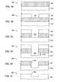
- Figures 1A-1F are cross-sectional views showing an etching sequence for processing an alternate phase shift photomask.
- Figure 2 is a block diagram of key components of an integrated etch system.
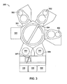
- Figure 3 is a diagram of one embodiment of an integrated etch system.
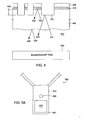
- Figure 4 is a schematic diagram showing a substrate, a measurement tool, and the impeding and reflected light beams between the substrate and the measurement tool.
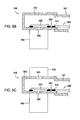
- Figure 5A shows a schematic drawing of the end of the robot arm with a robot blade.
- Figure 5B shows a schematic drawing of a measurement cell and an etch depth metrology tool.
- Figure 5C shows a schematic drawing of a measurement cell with an etch depth measurement tool and a CD measurement tool.
- the present invention is described herein primarily with reference to the etching of alternate phase shift masks.
- the concept of the invention can be used for etching other types of photomasks.
- FIGS 1A-1F illustrate an exemplary process flow of creating an alternate phase shift mask.
- a substrate 100 is introduced into a processing chamber.
- the substrate 100 (or reticle) comprises a base material of an optically transparent material 110, for example, optical quality quartz, calcium fluoride, alumina, sapphire, or combinations thereof, typically made of optical quality quartz material.
- An opaque (or light-shielding) metal layer 120 such as chromium, is deposited on the optically transparent material 110 as shown in Figure 1A.
- the light-shielding metal layer such as chromium layer, may be deposited by conventional methods known in the art, such as by physical vapor deposition (PVD) or chemical vapor deposition (CVD) techniques.
- PVD physical vapor deposition
- CVD chemical vapor deposition
- the light-shielding (or opaque) metal layer 120 is typically deposited to a thickness between about 50 and about 150 nanometers (nm) thick, however, the depth of the layer may change based upon the requirements of the manufacturer and the composition of the materials of the substrate or metal layer.
- the substrate 100 is then transferred to another processing chamber where a layer of resist material 130, such as "RISTON” resist, manufactured by Du Pont de Nemours Chemical Company, is deposited upon the opaque metal layer 120 to a thickness between about 200 and 600 nm thick.
- the resist material 130 is then pattern etched using conventional laser or electron beam patterning equipment to form a first opening 125 which is used to define the dimensions of the second opening 135 to be formed in the opaque metal layer 120.
- the substrate 100 is then transferred to an etch system, such as the Tetra IITM photomask etch chamber in the Tetra IITM photomask etch system described in Figure 3 (described below), manufactured by Applied Materials, Inc., of Santa Clara, California.
- an etch system such as the Tetra IITM photomask etch chamber in the Tetra IITM photomask etch system described in Figure 3 (described below), manufactured by Applied Materials, Inc., of Santa Clara, California.
- an inductively coupled plasma etch chamber that includes the Tetra IITM photomask etch chamber.
- other process chambers may be used to perform the processes of the invention, including, for example, capacitively coupled parallel plate chambers and magnetically enhanced ion etch chambers as well as inductively coupled plasma etch chambers of different designs.
- the light-shielding metal layer 120 is etched using metal etching techniques known in the art or by new metal etching techniques that may be developed to form the second opening 135 which expose the underlying transparent material 110 as shown in Figure 1C.
- the substrate 100 is transferred to a processing chamber, where the remaining resist material 130 is usually removed from the substrate 100.
- the resist removal could be accomplished by an oxygen plasma process or other resist removal technique known in the art.
- the substrate 100 may be further processed by etching the transparent material 110.
- the resist material 130 is removed and a second photoresist 140 is applied and patterned to expose the underlying transparent material 110 within the second opening 135.
- the resist material is deposited to a depth between about 200 nm and 600 nm thick, but may be of any thickness and may also be of the same thickness as the depth of the features to be etched in the transparent material 110 to form the photomask.
- the photoresist 140 is then etched to form a third opening 145 in the resist layer 140 and the metal layer 120.
- the patterned substrate 100 is then transferred to an etch chamber, such as the Tetra IITM photomask etch system described in Figure 3 (described below), for plasma etching the transparent material 310.
- the precise control of the etch depth 175 is very critical. For example, in order to achieve a phase shift angle of 180° for alternate phase shift mask for KrF excimer laser lithography, the quartz etch depth is about 2400 A. To avoid over-etch, the initial etching only etches partially, such as 50%-75%, of the targeted etch depth.
- the etch depth 175 (or phase shift angle) of the etched substrate 100 is measured at an integrated metrology tool. The substrate 100 subsequently undergoes additional etch and etch depth measurement until the targeted etch depth 175 is reached.
- Performing etch depth measurement in an integrated metrology tool has the advantage of avoiding the need of transferring the substrate to an area not under the same vacuum environment. Transferring substrates to an area not under the same vacuum environment repeatedly is time consuming, due to breaking vacuum, and could result in particle generation, which is very undesirable for photomask making.
- the second resist material 140 is then removed to form a patterned substrate surface 155.
- An alternate phase shift mask with a patterned substrate surface 165 is formed after the metal layer 120 is removed.
- dry etching in an etch chamber only etches to reach a percentage of the final etch depth and the final step is a wet etch step, since wet etch could reduce the surface roughness and could reduce the micro-trenching on the photomask substrate.
- Alternate phase shift photomask etching processes for light-shielding layers such as chromium, and optically transparent materials, such as quartz, include dry etching processes. Plasmas of etching gases, such as chlorine-containing gases (e.g. Cl 2 ) or fluorine-containing gases (e.g. SF 6 or CF 4 ), oxidizing gases, such as oxygen, and inert gases, such as helium, could be used to etch the metal layers formed on the substrate or the substrate itself. Details of etching chemistries that are used to etch light-shielding layer for this application have been disclosed in commonly assigned U.S.
- etching gases such as chlorine-containing gases (e.g. Cl 2 ) or fluorine-containing gases (e.g. SF 6 or CF 4 )
- oxidizing gases such as oxygen
- inert gases such as helium
- Etching of the silicon based material of the substrate is described in commonly assigned U.S. Patent Number 6,534,417, titled “Method and Apparatus For Etching Photomasks", issued March 18, 2003 and U.S. Patent Number 6,391,790, also titled “Method and Apparatus For Etching Photomasks", issued May 21, 2002.
- the disclosures of all of these applications are incorporated herein by reference to the extent not inconsistent with aspects of the invention.
- Etch depth metrology techniques as employed by the present invention are advanced process control (APC) enablers.
- Etch depth metrology techniques detect the reflection of a substrate over a broad wavelength range. The detected wavelength spectra are fitted to a theoretical model to enable the characterization of the film. The metrology can be used to measure transparency, etch depth, film thickness and phase shift angle at multiple locations on the substrate.
- An example of the etch depth (or phase shift angle) measuring tool is the n&k Analyzer 1512RT available from n&k Technology, Inc. of Santa Clara, CA.
- An exemplary embodiment of the present invention is implemented using a etch depth measuring tool in a processing system 200, as shown in Fig. 2, comprising a measuring tool 210, e.g., a etch depth (or phase shift angle) measurement tool.
- Processing system 200 further comprises a processor 220, which performs the analysis disclosed herein electronically, and a monitor 230 for displaying results of the analyses of processor 220.
- Processor 220 can be in communication with a memory device 240, such as a semiconductor memory, and a computer software-implemented database system 250 known as a "manufacturing execution system" (MES) conventionally used for storage of process information.
- MES manufacturing execution system
- Processor 220 can also be in communication with the measuring tool 210, and etcher 270.
- etch system that is integrated with an ex-situ metrology tool with the capability of measuring etch depth (or phase shift angle) is shown in Figure 3.
- the system, Tetra IITM comprises a chamber or "mainframe" 301, such as the CenturaTM processing system available from Applied Materials, Inc. of Santa Clara, California, for mounting a plurality of processing chambers, e.g., Tetra IITM photomask reactors (or chambers) 302, and one or more transfer chambers 303, also called "load locks".
- three etch reactors 302 and one metrology tool 306 are mounted to the mainframe 301.
- the metrology tool 306 can be placed under the same vacuum as the mainframe 301, since there is an opening (not shown) between the mainframe 301 and the metrology tool 306 to make them in fluid communication. In one exemplary embodiment, three etchers 302 are used for etching.
- a robot 304 is provided within the mainframe 301 for transferring wafers between the processing reactors 302, the transfer chambers 303, and an integrated metrology tool 306.
- the integrated metrology tool 306 can measure the etch depth (or phase shift angle).
- the transfer chambers 303 are connected to a factory interface 305, also known as a "mini environment", which maintains a controlled environment.
- the metrology (or measurement) tool 306, mounted to the mainframe 301 has high-speed data collection and analysis capabilities.
- Cassette holders 308 are connected to the other end of the factory interface 305.
- a robot 307 is placed inside 305 to transfer substrates between cassette holders (308), and "load locks" (303).
- the etch depth measurement tool 306 is mounted to the mainframe 301 to allow the etched substrate from the etch chamber 302 to be measured and be sent back to etch chamber 302 to be etched again.
- the etch and measurement process sequence could repeat several times until the targeted etch depth (or phase shift angle) is reached. Due to the nature of repeated etch and measurement to target etch depth of transparent material 110, it is desirable to have the etch depth measurement tool (or phase shift angle measurement tool) mounted to the mainframe 301.
- Both mainframe 301 and the metrology tool 306 are under integrated vacuum environment and can avoid the need of transferring the substrate to an area not under vacuum, which could be time consuming due to additional substrate transport and breaking the vacuum. Repeated transferring substrate between processing areas that are under vacuum and not under vacuum is not only time consuming, but also particle generating.
- the metrology tool 306 is placed at the location of one of the transfer chambers 303. Placing the metrology tool 306 at the location of one of the transfer chambers 303 also has the advantage of avoiding the need of transferring the substrate to an area not under vacuum.
- phase shift angle (or etch depth) can be measured by analyzing reflected light from the backside of the substrate, which does not require the removal the opaque film 320 and the photoresist film 340.
- Conventional phase shift angle measurement is performed from the substrate front side and requires the removal of the opaque film 320 and the photoresist film 340 prior to phase shift angle measurement.
- the additional processing steps of removing films can cause particles or other processing defects, which are highly undesirable for photomask preparation.
- the opaque film 320 and photoresist film 340 would need to be re-deposited and re-patterned again to allow further etching of the transparent material 310, which could worsen the particles and other processing defects problems.
- Figure 4 shows a schematic drawing of an etch depth measurement tool (or phase shift angle measurement tool) 460, placed below the backside of a substrate 400.
- the substrate 400 has an etch depth 450 and also has an opaque film 410 and a photoresist film 420 on the front side.
- On the back side of the substrate 400 there are incident light beams 430, 430 and 432, and reflected light beams 430', 431' and 432'.
- the light source of incident light beams could be from the measurement tool 460.
- the light source is preferably a broadband light source. Part of incident light beam 430, reflected light beam 430', is reflected from the interface between the substrate 400 and the environment 470.
- Reflected light beam 431' is reflected from the interface between the substrate etch interface 451 with the environment 470.
- Reflected light beam 432' is reflected from the interface between the opaque layer 410 and the substrate 400.
- the etch depth measurement tool collects reflected light beams over a range of substrate backside surface. By calculating the phase shift between the light beams such as 431' and 432', the etch depth 450 and the phase shift of the transparent substrate can be determined without removing the films on the front side, such as opaque film 410 and photoresist film 420, of the substrate 400.
- a robot arm 500 which is part of robot 304 of the mainframe 301 of Figure 3, is designed to include a substrate holder 501.
- the substrate holder 501 has an opening that allows the incident light beams and reflected light beams on the substrate backside to pass through, as shown in Figure 5A.
- Figure 5A shows a schematic drawing of the end of the robot arm 500 that contains a robot blade 510, which has a substrate holder 501.
- the substrate holder 501 has an aperture 502 that is proportional to the size of the substrate.
- the aperture 502 is about 4 inches by 4 inches for a 6 inches by 6 inches substrate.
- the size of the aperture 502 is smaller than the size of the substrate to allow the edge of the substrate to be supported by the substrate holder.
- the thickness of the robot blade 510 is about 2/5 inch (1.02 cm).
- the size of the aperture 502 should be as large as possible to allow measurement data to be collected across large area on the substrate.
- FIG. 5B shows the substrate 520 is placed inside the metrology tool 306 of Figure 3.
- the metrology tool 306 comprises a measurement cell 550 and an etch depth measurement tool 460.
- the substrate is moved by the robot arm 500 to be over the measurement point.
- Underneath the measurement point 560 is a etch depth measurement tool 460.
- the etch depth measurement tool 460 comprises a broadband light source (not shown), which emits light to the backside of the substrate 520.
- the robot blade 510 is attached to the robot arm 500 and it has roll and tilt function to allow the surface of substrate 520 to be perpendicular to the measurement light beam emitted from the measurement tool 460.
- the etch depth measurement tool 460 collects the reflected light from the substrate backside.
- the data generated from the reflected light are analyzed to calculate the etch depth by the measurement tool 460.
- a calibration pad 580 which contains an etch depth measurement calibration device, such as a piece of bare silicon, on the robot blade 510.
- the size of the calibration pad is about 1/2 inch (1.27 cm) in diameter.
- the calibration pad 580 can be moved to be above the measurement point 560 to calibrate the measurement tool 460.
- a native oxide layer is typically present on the bare silicon surface. The presence of the native oxide layer is important for calibration of some measurement tools.
- the measurement point 560 is a circular opening with a diameter, such as about 1 inch (2.54 cm).
- backside etch depth measurement is that the measurement does not require the removal of the front side films. Therefore the substrate can be partially etched first, then be measured to target the next etch amount. The substrate can then be re-etched and re-measured multiple times with out the need of moving the substrate to another system to perform photoresist layer stripping.
- the precise control of the phase shift angle (or etch depth) is very critical. Since the substrate is transparent and the phase shift angle can be measured from the backside, the processing time can be greatly reduced, since the fine tuning of the substrate etch does not require removal of the substrate from the etching module.
- a CD measurement tool 590 is mounted on top of the measurement cell 306 to collect critical dimension (CD) measurement data through an opening 595 (as shown in Figure 5C).
- the collected CD measurement data can be fed forward and backward to the etcher to adjust the substrate etch recipe. Since CD measurement has more stringent measurement location requirement than etch depth measurement, the robot arm 500, which is part of robot 304 in the mainframe 301, might not have sufficient precision control as required.
- the CD measurement tool 590 could include a moving device (not shown), to allow a measuring device (not shown) in the CD measurement tool to be moved over to a particular measurement location above the substrate 520. The movement of the moving device is controlled by a controller to control its precise movement.
- Figure 5C shows a schematic drawing of metrology cell 306 with a top CD measurement tool 590 and a bottom etch depth measurement tool 460.
- the CD measurement tool 590 can employ OCD (optical critical dimension) metrology techniques.
- OCD metrology techniques are advanced process control (APC) enablers.
- APC advanced process control
- normal incidence spectroscopic OCD metrology systems provide detailed line profiles not possible with in-line non-destructive SEMs.
- the OCD metrology can operate under reflective mode (utilizing reflected light) or transmission mode (utilizing transmitted light).
- the compact size and speed of OCD technology enables the measurement system of the present invention to be fully integrated into a process tool, such as Applied Materials' Tetra IITM or DPS® II etch system. When combined with APC software, this provides a complete, feed-forward solution for wafer-to-wafer closed loop control.
- optical CD measuring tool is the Nano OCD 9000 available from Nanometrics of Milpitas, CA, or an optical imager as disclosed in U.S. Patent 5,963,329.
- the optical CD measuring tool can utilize scatterometry, reflectometry or transmission ellipsometry techniques.
Landscapes
- Engineering & Computer Science (AREA)
- Physics & Mathematics (AREA)
- General Physics & Mathematics (AREA)
- Computer Hardware Design (AREA)
- Condensed Matter Physics & Semiconductors (AREA)
- Manufacturing & Machinery (AREA)
- Robotics (AREA)
- Microelectronics & Electronic Packaging (AREA)
- Power Engineering (AREA)
- Preparing Plates And Mask In Photomechanical Process (AREA)
- Drying Of Semiconductors (AREA)
- Length Measuring Devices By Optical Means (AREA)
- Exposure And Positioning Against Photoresist Photosensitive Materials (AREA)
- Testing Or Measuring Of Semiconductors Or The Like (AREA)
Applications Claiming Priority (1)
| Application Number | Priority Date | Filing Date | Title |
|---|---|---|---|
| US11/031,400 US20060154388A1 (en) | 2005-01-08 | 2005-01-08 | Integrated metrology chamber for transparent substrates |
Publications (1)
| Publication Number | Publication Date |
|---|---|
| EP1679548A1 true EP1679548A1 (en) | 2006-07-12 |
Family
ID=36098810
Family Applications (1)
| Application Number | Title | Priority Date | Filing Date |
|---|---|---|---|
| EP06250044A Withdrawn EP1679548A1 (en) | 2005-01-08 | 2006-01-05 | Apparatus and method for measuring etch depth of a substrate |
Country Status (5)
| Country | Link |
|---|---|
| US (2) | US20060154388A1 (enExample) |
| EP (1) | EP1679548A1 (enExample) |
| JP (1) | JP5392972B2 (enExample) |
| KR (1) | KR101252068B1 (enExample) |
| TW (1) | TWI375288B (enExample) |
Cited By (2)
| Publication number | Priority date | Publication date | Assignee | Title |
|---|---|---|---|---|
| TWI512393B (zh) * | 2012-08-03 | 2015-12-11 | Applied Materials Inc | 光罩製造應用中之用於蝕刻石英基板的裝置及方法 |
| TWI752019B (zh) * | 2016-04-12 | 2022-01-11 | 台灣積體電路製造股份有限公司 | 具有多層遮光層的光罩 |
Families Citing this family (24)
| Publication number | Priority date | Publication date | Assignee | Title |
|---|---|---|---|---|
| US20050197721A1 (en) * | 2004-02-20 | 2005-09-08 | Yung-Cheng Chen | Control of exposure energy on a substrate |
| US7601272B2 (en) * | 2005-01-08 | 2009-10-13 | Applied Materials, Inc. | Method and apparatus for integrating metrology with etch processing |
| US20060154388A1 (en) * | 2005-01-08 | 2006-07-13 | Richard Lewington | Integrated metrology chamber for transparent substrates |
| CN100459087C (zh) * | 2006-07-21 | 2009-02-04 | 中芯国际集成电路制造(上海)有限公司 | 确定半导体特征的方法和用于制造集成电路的方法 |
| US8012857B2 (en) * | 2007-08-07 | 2011-09-06 | Semiconductor Components Industries, Llc | Semiconductor die singulation method |
| US8859396B2 (en) | 2007-08-07 | 2014-10-14 | Semiconductor Components Industries, Llc | Semiconductor die singulation method |
| KR20100061731A (ko) * | 2007-09-14 | 2010-06-08 | 퀄컴 엠이엠스 테크놀로지스, 인크. | Mems 제조에 이용되는 에칭 방법 |
| US7765077B2 (en) * | 2007-09-21 | 2010-07-27 | Tokyo Electron Limited | Method and apparatus for creating a Spacer-Optimization (S-O) library |
| CN101889325B (zh) * | 2007-12-06 | 2014-05-07 | 因特瓦克公司 | 用于衬底的两侧溅射蚀刻的系统和方法 |
| US7935464B2 (en) * | 2008-10-30 | 2011-05-03 | Applied Materials, Inc. | System and method for self-aligned dual patterning |
| US7904273B2 (en) * | 2009-02-16 | 2011-03-08 | International Business Machines Corporation | In-line depth measurement for thru silicon via |
| US8232115B2 (en) | 2009-09-25 | 2012-07-31 | International Business Machines Corporation | Test structure for determination of TSV depth |
| US9136173B2 (en) | 2012-11-07 | 2015-09-15 | Semiconductor Components Industries, Llc | Singulation method for semiconductor die having a layer of material along one major surface |
| US9484260B2 (en) | 2012-11-07 | 2016-11-01 | Semiconductor Components Industries, Llc | Heated carrier substrate semiconductor die singulation method |
| US20150132959A1 (en) * | 2013-11-08 | 2015-05-14 | Leonard TEDESCHI | Pattern formation and transfer directly on silicon based films |
| US10840102B2 (en) * | 2013-11-27 | 2020-11-17 | Taiwan Semiconductor Manufacturing Co., Ltd. | Integrated system, integrated system operation method and film treatment method |
| US9418894B2 (en) | 2014-03-21 | 2016-08-16 | Semiconductor Components Industries, Llc | Electronic die singulation method |
| US9385041B2 (en) | 2014-08-26 | 2016-07-05 | Semiconductor Components Industries, Llc | Method for insulating singulated electronic die |
| US10366923B2 (en) | 2016-06-02 | 2019-07-30 | Semiconductor Components Industries, Llc | Method of separating electronic devices having a back layer and apparatus |
| US10373869B2 (en) | 2017-05-24 | 2019-08-06 | Semiconductor Components Industries, Llc | Method of separating a back layer on a substrate using exposure to reduced temperature and related apparatus |
| US12112959B2 (en) | 2018-09-04 | 2024-10-08 | Tokyo Electron Limited | Processing systems and platforms for roughness reduction of materials using illuminated etch solutions |
| KR102740093B1 (ko) * | 2018-12-14 | 2024-12-06 | 도쿄엘렉트론가부시키가이샤 | 조명된 에칭 용액을 사용하여 재료의 거칠기를 감소시키기 위한 공정 시스템 및 플랫폼 |
| US10818551B2 (en) | 2019-01-09 | 2020-10-27 | Semiconductor Components Industries, Llc | Plasma die singulation systems and related methods |
| JP7365878B2 (ja) * | 2019-12-06 | 2023-10-20 | 東京エレクトロン株式会社 | 計測装置及び計測方法 |
Citations (5)
| Publication number | Priority date | Publication date | Assignee | Title |
|---|---|---|---|---|
| US6129807A (en) * | 1997-10-06 | 2000-10-10 | Applied Materials, Inc. | Apparatus for monitoring processing of a substrate |
| US6411389B1 (en) * | 2000-05-03 | 2002-06-25 | The Regents Of The University Of Claifornia | Optical monitor for real time thickness change measurements via lateral-translation induced phase-stepping interferometry |
| US6413147B1 (en) * | 1993-09-16 | 2002-07-02 | Herbert E. Litvak | Optical techniques of measuring endpoint during the processing of material layers in an optically hostile environment |
| WO2004030050A2 (en) * | 2002-09-25 | 2004-04-08 | Lam Research Corporation | Apparatus and method for controlling etch depth |
| US20040203177A1 (en) * | 2003-04-11 | 2004-10-14 | Applied Materials, Inc. | Method and system for monitoring an etch process |
Family Cites Families (75)
| Publication number | Priority date | Publication date | Assignee | Title |
|---|---|---|---|---|
| JPS5795056A (en) * | 1980-12-05 | 1982-06-12 | Hitachi Ltd | Appearance inspecting process |
| JPS61290312A (ja) | 1985-06-19 | 1986-12-20 | Hitachi Ltd | 断面形状測定装置 |
| US5109430A (en) * | 1986-07-22 | 1992-04-28 | Schlumberger Technologies, Inc. | Mask alignment and measurement of critical dimensions in integrated circuits |
| US4767496A (en) * | 1986-12-11 | 1988-08-30 | Siemens Aktiengesellschaft | Method for controlling and supervising etching processes |
| US4911103A (en) * | 1987-07-17 | 1990-03-27 | Texas Instruments Incorporated | Processing apparatus and method |
| JPH0492444A (ja) * | 1990-08-08 | 1992-03-25 | Hitachi Ltd | 処理方法および装置 |
| US5171393A (en) * | 1991-07-29 | 1992-12-15 | Moffat William A | Wafer processing apparatus |
| US5499733A (en) * | 1992-09-17 | 1996-03-19 | Luxtron Corporation | Optical techniques of measuring endpoint during the processing of material layers in an optically hostile environment |
| US5653894A (en) * | 1992-12-14 | 1997-08-05 | Lucent Technologies Inc. | Active neural network determination of endpoint in a plasma etch process |
| US5452521A (en) * | 1994-03-09 | 1995-09-26 | Niewmierzycki; Leszek | Workpiece alignment structure and method |
| US5607800A (en) | 1995-02-15 | 1997-03-04 | Lucent Technologies Inc. | Method and arrangement for characterizing micro-size patterns |
| US5711849A (en) * | 1995-05-03 | 1998-01-27 | Daniel L. Flamm | Process optimization in gas phase dry etching |
| US6001699A (en) * | 1996-01-23 | 1999-12-14 | Intel Corporation | Highly selective etch process for submicron contacts |
| US5798529A (en) * | 1996-05-28 | 1998-08-25 | International Business Machines Corporation | Focused ion beam metrology |
| US6060022A (en) * | 1996-07-05 | 2000-05-09 | Beckman Coulter, Inc. | Automated sample processing system including automatic centrifuge device |
| US5944940A (en) * | 1996-07-09 | 1999-08-31 | Gamma Precision Technology, Inc. | Wafer transfer system and method of using the same |
| US6143081A (en) * | 1996-07-12 | 2000-11-07 | Tokyo Electron Limited | Film forming apparatus and method, and film modifying apparatus and method |
| US5948203A (en) * | 1996-07-29 | 1999-09-07 | Taiwan Semiconductor Manufacturing Company, Ltd. | Optical dielectric thickness monitor for chemical-mechanical polishing process monitoring |
| US5913102A (en) * | 1997-03-20 | 1999-06-15 | Taiwan Semiconductor Manufacturing Company, Ltd. | Method for forming patterned photoresist layers with enhanced critical dimension uniformity |
| US5926690A (en) * | 1997-05-28 | 1999-07-20 | Advanced Micro Devices, Inc. | Run-to-run control process for controlling critical dimensions |
| US5976740A (en) * | 1997-08-28 | 1999-11-02 | International Business Machines Corporation | Process for controlling exposure dose or focus parameters using tone reversing pattern |
| US5965309A (en) * | 1997-08-28 | 1999-10-12 | International Business Machines Corporation | Focus or exposure dose parameter control system using tone reversing patterns |
| US6161054A (en) * | 1997-09-22 | 2000-12-12 | On-Line Technologies, Inc. | Cell control method and apparatus |
| US6124212A (en) * | 1997-10-08 | 2000-09-26 | Taiwan Semiconductor Manufacturing Co. | High density plasma (HDP) etch method for suppressing micro-loading effects when etching polysilicon layers |
| US5963329A (en) * | 1997-10-31 | 1999-10-05 | International Business Machines Corporation | Method and apparatus for measuring the profile of small repeating lines |
| US6148239A (en) * | 1997-12-12 | 2000-11-14 | Advanced Micro Devices, Inc. | Process control system using feed forward control threads based on material groups |
| US6054710A (en) * | 1997-12-18 | 2000-04-25 | Cypress Semiconductor Corp. | Method and apparatus for obtaining two- or three-dimensional information from scanning electron microscopy |
| US6452677B1 (en) * | 1998-02-13 | 2002-09-17 | Micron Technology Inc. | Method and apparatus for detecting defects in the manufacture of an electronic device |
| US6033814A (en) * | 1998-02-26 | 2000-03-07 | Micron Technology, Inc. | Method for multiple process parameter matching |
| US6067357A (en) * | 1998-03-04 | 2000-05-23 | Genesys Telecommunications Laboratories Inc. | Telephony call-center scripting by Petri Net principles and techniques |
| IL125338A0 (en) * | 1998-07-14 | 1999-03-12 | Nova Measuring Instr Ltd | Method and apparatus for monitoring and control of photolithography exposure and processing tools |
| JP4601744B2 (ja) * | 1998-07-14 | 2010-12-22 | ノバ メジャリング インスツルメンツ リミテッド | フォトリソグラフィープロセスを制御するための方法およびシステム |
| US6424733B2 (en) * | 1998-07-20 | 2002-07-23 | Micron Technology, Inc. | Method and apparatus for inspecting wafers |
| US6183594B1 (en) * | 1998-09-25 | 2001-02-06 | International Business Machines Corporation | Method and system for detecting the end-point in etching processes |
| JP3090139B1 (ja) * | 1999-03-05 | 2000-09-18 | ミノルタ株式会社 | プロジェクタ用光学系 |
| WO2000058188A1 (en) * | 1999-03-25 | 2000-10-05 | N & K Technology, Inc. | Wafer handling robot having x-y stage for wafer handling and positioning |
| US6455437B1 (en) * | 1999-04-07 | 2002-09-24 | Applied Materials Inc. | Method and apparatus for monitoring the process state of a semiconductor device fabrication process |
| EP1065567A3 (en) * | 1999-06-29 | 2001-05-16 | Applied Materials, Inc. | Integrated critical dimension control |
| US6166509A (en) * | 1999-07-07 | 2000-12-26 | Applied Materials, Inc. | Detection system for substrate clamp |
| US6368975B1 (en) * | 1999-07-07 | 2002-04-09 | Applied Materials, Inc. | Method and apparatus for monitoring a process by employing principal component analysis |
| US6583065B1 (en) | 1999-08-03 | 2003-06-24 | Applied Materials Inc. | Sidewall polymer forming gas additives for etching processes |
| EP1079426A1 (en) | 1999-08-16 | 2001-02-28 | Applied Materials, Inc. | Integration scheme using selfplanarized dielectric layer for shallow trench isolation (STI) |
| US6225639B1 (en) | 1999-08-27 | 2001-05-01 | Agere Systems Guardian Corp. | Method of monitoring a patterned transfer process using line width metrology |
| US6707544B1 (en) | 1999-09-07 | 2004-03-16 | Applied Materials, Inc. | Particle detection and embedded vision system to enhance substrate yield and throughput |
| US6721045B1 (en) * | 1999-09-07 | 2004-04-13 | Applied Materials, Inc. | Method and apparatus to provide embedded substrate process monitoring through consolidation of multiple process inspection techniques |
| US6413867B1 (en) * | 1999-12-23 | 2002-07-02 | Applied Materials, Inc. | Film thickness control using spectral interferometry |
| JP3974319B2 (ja) * | 2000-03-30 | 2007-09-12 | 株式会社東芝 | エッチング方法 |
| EP1269521A1 (en) * | 2000-04-07 | 2003-01-02 | Varian Semiconductor Equipment Associates Inc. | WAFER ORIENTATION SENSOR FOR GaAs WAFERS |
| US6245581B1 (en) * | 2000-04-19 | 2001-06-12 | Advanced Micro Devices, Inc. | Method and apparatus for control of critical dimension using feedback etch control |
| WO2001084382A1 (en) | 2000-05-04 | 2001-11-08 | Kla-Tencor, Inc. | Methods and systems for lithography process control |
| US6625512B1 (en) | 2000-07-25 | 2003-09-23 | Advanced Micro Devices, Inc. | Method and apparatus for performing final critical dimension control |
| IL139368A (en) | 2000-10-30 | 2006-12-10 | Nova Measuring Instr Ltd | Process control for microlithography |
| US6625497B2 (en) * | 2000-11-20 | 2003-09-23 | Applied Materials Inc. | Semiconductor processing module with integrated feedback/feed forward metrology |
| US20020147960A1 (en) * | 2001-01-26 | 2002-10-10 | Applied Materials, Inc. | Method and apparatus for determining scheduling for wafer processing in cluster tools with integrated metrology and defect control |
| US6653231B2 (en) * | 2001-03-28 | 2003-11-25 | Advanced Micro Devices, Inc. | Process for reducing the critical dimensions of integrated circuit device features |
| US6525829B1 (en) * | 2001-05-25 | 2003-02-25 | Novellus Systems, Inc. | Method and apparatus for in-situ measurement of thickness of copper oxide film using optical reflectivity |
| US6479309B1 (en) * | 2001-05-25 | 2002-11-12 | Advanced Micro Devices, Inc. | Method and apparatus for determining process layer conformality |
| US20030000922A1 (en) * | 2001-06-27 | 2003-01-02 | Ramkumar Subramanian | Using scatterometry to develop real time etch image |
| US6649426B2 (en) | 2001-06-28 | 2003-11-18 | Advanced Micro Devices, Inc. | System and method for active control of spacer deposition |
| US20030045098A1 (en) * | 2001-08-31 | 2003-03-06 | Applied Materials, Inc. | Method and apparatus for processing a wafer |
| US20030052084A1 (en) * | 2001-09-18 | 2003-03-20 | Tabery Cyrus E. | In-situ or ex-situ profile monitoring of phase openings on alternating phase shifting masks by scatterometry |
| US20030092281A1 (en) * | 2001-11-13 | 2003-05-15 | Chartered Semiconductors Manufactured Limited | Method for organic barc and photoresist trimming process |
| US6960416B2 (en) * | 2002-03-01 | 2005-11-01 | Applied Materials, Inc. | Method and apparatus for controlling etch processes during fabrication of semiconductor devices |
| JP4197103B2 (ja) | 2002-04-15 | 2008-12-17 | 株式会社荏原製作所 | ポリッシング装置 |
| US6762130B2 (en) * | 2002-05-31 | 2004-07-13 | Texas Instruments Incorporated | Method of photolithographically forming extremely narrow transistor gate elements |
| US6825487B2 (en) * | 2002-07-30 | 2004-11-30 | Seh America, Inc. | Method for isolation of wafer support-related crystal defects |
| JP4584531B2 (ja) * | 2002-08-02 | 2010-11-24 | 株式会社日立製作所 | 異物モニタリングシステム |
| US20040200574A1 (en) * | 2003-04-11 | 2004-10-14 | Applied Materials, Inc. | Method for controlling a process for fabricating integrated devices |
| US7094613B2 (en) * | 2003-10-21 | 2006-08-22 | Applied Materials, Inc. | Method for controlling accuracy and repeatability of an etch process |
| US7250309B2 (en) * | 2004-01-09 | 2007-07-31 | Applied Materials, Inc. | Integrated phase angle and optical critical dimension measurement metrology for feed forward and feedback process control |
| KR100568867B1 (ko) * | 2004-03-18 | 2006-04-10 | 삼성전자주식회사 | 웨이퍼 좌표감지장치 및 그 웨이퍼 좌표감지 기능을 갖는반도체 제조설비 |
| US7076320B1 (en) * | 2004-05-04 | 2006-07-11 | Advanced Micro Devices, Inc. | Scatterometry monitor in cluster process tool environment for advanced process control (APC) |
| US6961626B1 (en) * | 2004-05-28 | 2005-11-01 | Applied Materials, Inc | Dynamic offset and feedback threshold |
| US20060154388A1 (en) * | 2005-01-08 | 2006-07-13 | Richard Lewington | Integrated metrology chamber for transparent substrates |
| US7601272B2 (en) * | 2005-01-08 | 2009-10-13 | Applied Materials, Inc. | Method and apparatus for integrating metrology with etch processing |
-
2005
- 2005-01-08 US US11/031,400 patent/US20060154388A1/en not_active Abandoned
-
2006
- 2006-01-02 TW TW095100110A patent/TWI375288B/zh not_active IP Right Cessation
- 2006-01-05 EP EP06250044A patent/EP1679548A1/en not_active Withdrawn
- 2006-01-06 KR KR1020060001698A patent/KR101252068B1/ko not_active Expired - Fee Related
- 2006-01-10 JP JP2006002870A patent/JP5392972B2/ja not_active Expired - Fee Related
- 2006-09-15 US US11/532,195 patent/US7846848B2/en active Active
Patent Citations (5)
| Publication number | Priority date | Publication date | Assignee | Title |
|---|---|---|---|---|
| US6413147B1 (en) * | 1993-09-16 | 2002-07-02 | Herbert E. Litvak | Optical techniques of measuring endpoint during the processing of material layers in an optically hostile environment |
| US6129807A (en) * | 1997-10-06 | 2000-10-10 | Applied Materials, Inc. | Apparatus for monitoring processing of a substrate |
| US6411389B1 (en) * | 2000-05-03 | 2002-06-25 | The Regents Of The University Of Claifornia | Optical monitor for real time thickness change measurements via lateral-translation induced phase-stepping interferometry |
| WO2004030050A2 (en) * | 2002-09-25 | 2004-04-08 | Lam Research Corporation | Apparatus and method for controlling etch depth |
| US20040203177A1 (en) * | 2003-04-11 | 2004-10-14 | Applied Materials, Inc. | Method and system for monitoring an etch process |
Non-Patent Citations (1)
| Title |
|---|
| COLLARD ET AL: "Integrated phase shift measurements for advanced mask etch process control", PROCEEDINGS OF THE SPIE - THE INTERNATIONAL SOCIETY FOR OPTICAL ENGINEERING SPIE-INT. SOC. OPT. ENG USA, vol. 5256, 2003, pages 76 - 84, XP002376855 * |
Cited By (2)
| Publication number | Priority date | Publication date | Assignee | Title |
|---|---|---|---|---|
| TWI512393B (zh) * | 2012-08-03 | 2015-12-11 | Applied Materials Inc | 光罩製造應用中之用於蝕刻石英基板的裝置及方法 |
| TWI752019B (zh) * | 2016-04-12 | 2022-01-11 | 台灣積體電路製造股份有限公司 | 具有多層遮光層的光罩 |
Also Published As
| Publication number | Publication date |
|---|---|
| US20060154388A1 (en) | 2006-07-13 |
| TW200633107A (en) | 2006-09-16 |
| JP5392972B2 (ja) | 2014-01-22 |
| JP2006194878A (ja) | 2006-07-27 |
| US20070012660A1 (en) | 2007-01-18 |
| US7846848B2 (en) | 2010-12-07 |
| KR101252068B1 (ko) | 2013-04-15 |
| KR20060081365A (ko) | 2006-07-12 |
| TWI375288B (en) | 2012-10-21 |
Similar Documents
| Publication | Publication Date | Title |
|---|---|---|
| US7846848B2 (en) | Cluster tool with integrated metrology chamber for transparent substrates | |
| US7250309B2 (en) | Integrated phase angle and optical critical dimension measurement metrology for feed forward and feedback process control | |
| TWI387039B (zh) | 整合測量法與蝕刻製程的方法及設備 | |
| US7085676B2 (en) | Feed forward critical dimension control | |
| JP2019507375A (ja) | パターン形成プロセスを制御する方法、リソグラフィ装置、メトロロジ装置リソグラフィックセル、および関連するコンピュータプログラム | |
| US10453696B2 (en) | Dual endpoint detection for advanced phase shift and binary photomasks | |
| US7733502B2 (en) | Roughness evaluation method and system | |
| CN101055422B (zh) | 用于透明基材的整合式测量室 | |
| US6447962B2 (en) | Method for repairing MoSi attenuated phase shift masks | |
| US7759136B2 (en) | Critical dimension (CD) control by spectrum metrology | |
| JPH0682727B2 (ja) | 検査用基板とその製造方法 | |
| US6872497B1 (en) | Reflective mask for short wavelength lithography | |
| HK1114426A (en) | Integrated metrology chamber for transparent substrates | |
| JP2731914B2 (ja) | 検査用基板およびその製造方法 | |
| US20060065626A1 (en) | Detection and feed forward of exposed area to improve plasma etching | |
| TW201719277A (zh) | 修復光罩的方法 | |
| Cummings et al. | Back to square 9: a demonstration of 9-in. reticle capablilty | |
| Moreau | Process Controls | |
| Smith | Dimensional metrology for partially etched photomasks in iterative-etch fabrication processes | |
| Dieu et al. | Advanced 193 tri-tone EAPSM (9% to 18%) for 65-nm node |
Legal Events
| Date | Code | Title | Description |
|---|---|---|---|
| PUAI | Public reference made under article 153(3) epc to a published international application that has entered the european phase |
Free format text: ORIGINAL CODE: 0009012 |
|
| AK | Designated contracting states |
Kind code of ref document: A1 Designated state(s): AT BE BG CH CY CZ DE DK EE ES FI FR GB GR HU IE IS IT LI LT LU LV MC NL PL PT RO SE SI SK TR |
|
| AX | Request for extension of the european patent |
Extension state: AL BA HR MK YU |
|
| 17P | Request for examination filed |
Effective date: 20070112 |
|
| 17Q | First examination report despatched |
Effective date: 20070220 |
|
| AKX | Designation fees paid |
Designated state(s): AT BE BG CH CY CZ DE DK EE ES FI FR GB GR HU IE IS IT LI LT LU LV MC NL PL PT RO SE SI SK TR |
|
| STAA | Information on the status of an ep patent application or granted ep patent |
Free format text: STATUS: THE APPLICATION HAS BEEN WITHDRAWN |
|
| 18W | Application withdrawn |
Effective date: 20100325 |