EP1669987B1 - Optischer Kopf mit Strahleneingangs-/ausgangskoppler auf einem planaren Wellenleiter - Google Patents
Optischer Kopf mit Strahleneingangs-/ausgangskoppler auf einem planaren Wellenleiter Download PDFInfo
- Publication number
- EP1669987B1 EP1669987B1 EP05257138A EP05257138A EP1669987B1 EP 1669987 B1 EP1669987 B1 EP 1669987B1 EP 05257138 A EP05257138 A EP 05257138A EP 05257138 A EP05257138 A EP 05257138A EP 1669987 B1 EP1669987 B1 EP 1669987B1
- Authority
- EP
- European Patent Office
- Prior art keywords
- planar waveguide
- optical head
- coupler
- leaky
- disc
- Prior art date
- Legal status (The legal status is an assumption and is not a legal conclusion. Google has not performed a legal analysis and makes no representation as to the accuracy of the status listed.)
- Expired - Lifetime
Links
Images




Classifications
-
- G—PHYSICS
- G11—INFORMATION STORAGE
- G11B—INFORMATION STORAGE BASED ON RELATIVE MOVEMENT BETWEEN RECORD CARRIER AND TRANSDUCER
- G11B7/00—Recording or reproducing by optical means, e.g. recording using a thermal beam of optical radiation by modifying optical properties or the physical structure, reproducing using an optical beam at lower power by sensing optical properties; Record carriers therefor
- G11B7/12—Heads, e.g. forming of the optical beam spot or modulation of the optical beam
- G11B7/123—Integrated head arrangements, e.g. with source and detectors mounted on the same substrate
- G11B7/124—Integrated head arrangements, e.g. with source and detectors mounted on the same substrate the integrated head arrangements including waveguides
Definitions
- the present invention relates generally to an optical head recording and/or reproducing information on or from an optical or magneto-optical disc (disk) using optical or magneto-optical characteristics, and more particularly, to an optical head having an innovatively reduced thickness.
- optical heads are used to record and/or reproduce information on or from compact discs (CDs), digital versatile discs (DVDs), blue-ray discs (BDs), or MP3 players using optical discs.
- An optical head includes many individual optical parts such as the light transmitting/receiving elements (i.e., the light emitting/receiving elements including a laser diode (LD) and a photo diode (PD)), a mirror, a prism, a beam splitter (BS), a polarization beam splitter (PBS), and a hologram optical element (HOE).
- the light transmitting/receiving elements i.e., the light emitting/receiving elements including a laser diode (LD) and a photo diode (PD)
- a mirror i.e., the light emitting/receiving elements including a laser diode (LD) and a photo diode (PD)
- BS beam splitter
- PBS polarization beam splitter
- An optical head is made by assembling these individual optical parts each of which has thickness and volume in the 3-dimensional space, and this is an obstacle to reducing the overall thickness of the optical head.
- reduction of the optical head thickness is an important design requirement of the modern mobile optical disc devices, which are no longer stationary but are portable devices, i.e., easily carryable and movable. To achieve this, the thickness of the optical head must be innovatively reduced.
- FIG. 1 is a cross-sectional view of an example of an optical head used in an MP3 player according to prior art.
- the optical head shown in FIG. 1 is published in PCT International Application No. PCT/US02/00875 and PCT International Publication No. WO 02/058059 A2 , entitled "Beamshaper for Optical Head” by Dataplay, INC.
- an LD 4, a PD 6, an objective lens 8, a prism 10, a mirror 12, and a PBS 14 are disposed 3-dimensionally on a substrate 2.
- the beam 20 emitted from the LD 4 is incident on a disc 16 through the prism 10, the mirror 12, the PBS 14, and the objective lens 8.
- the beam 20 is reflected from the disc 16 and then incident on the PD 6 through the PBS 14.
- each of the optical parts in the optical head as shown in FIG. 1 has a predetermined volume and disposed in the 3-dimensional space, the overall thickness of the optical head, even if the objective lens 8 is excluded, ends up being undesirably large for mobility. This also means that the overall thickness of an optical head such as that shown in FIG. 1 may not be readily reduced as long as many individual parts as shown in FIG. 1 are assembled into an optical head, mainly because the thickness of each of the individual parts will add up.
- FIG. 2 is a cross-sectional view of another prior art example of an optical head for a BD using a blue laser beam manufactured by Sony Corporation.
- the optical head shown in FIG. 2 is published in February 2003, entitled " Small Integrated Optical Head Device Using a Blue-violet Laser Diode for Blue-ray Disc System," Jpn. J. Appl. Phys. Vol. 42(2003), pp. 880-884, Part 1. No. 2B .
- the optical head shown in FIG. 2 includes optical parts such as a blue beam LD 30, a 45 degree mirror 32, a half wave plate (HWP) 34, a grating 36, a PBS 38, a mirror 40, a HOE 42, a cylinder lens 44, a prism 46, a molded optical element, a PD IC 50, and a package 54 molded by a lead frame 52.
- optical parts such as a blue beam LD 30, a 45 degree mirror 32, a half wave plate (HWP) 34, a grating 36, a PBS 38, a mirror 40, a HOE 42, a cylinder lens 44, a prism 46, a molded optical element, a PD IC 50, and a package 54 molded by a lead frame 52.
- HWP half wave plate
- the beam 56 emitted from the blue beam LD 30 is incident on a disc through the 45 degree mirror 32, the HWP 34, the grating 36, and the PBS 38.
- the beam 56 is reflected from the disc and then incident on the PD IC 50 through the PBS 38, the mirror 40, the HOE 42, and the cylinder lens 44.
- optical parts in the optical head shown in FIG. 2 are also disposed in a 3-dimensional space.
- the HOE 42 is used; however, the overall thickness of the optical head still cannot be sufficiently and greatly reduced because the individual parts each occupying a predetermined volume in the 3-dimensional space are still used to assemble the optical head shown in FIG. 2 .
- the optical parts in a conventional optical head are disposed in a 3-dimensional space. This limits effective reduction of the overall thickness of a conventional optical head. As a result, the undesirable thickness of the conventional optical heads presents a fundamental obstacle to putting them together in an easily carryable, mobile optical disc for its intended practical portable use.
- An optical head is disclosed in US-A-5,701,289 , which is used for the two-part form delimitation, which includes a beam-generator, a slab type waveguide, an output hologram coupler, a focal lens, an input hologram coupler and a photoelectric transducer.
- DE-A-39 21 406 discloses an optical integrated circuit and an optical apparatus used in optical communication or an opto-electronics apparatus such as an optical disk recording apparatus, in which various kinds of aberration arise, caused by wavelength variation of a light source when a semiconductor laser is used as the light source.
- a leaky-mode directional coupler, for a blue laser waveguide lens, consisting of two slab waveguides is disclosed in Y. Park and D. Suh, "A Leaky-Mode Directional Coupler for a Blue Laser Waveguide Lens," in Diffractive Optics and Micro-Optics, OSA Technical Digest (Optical Society of America, 2004), paper DSuB3 .
- the present invention provides an optical head including optical parts that are not disposed on a 3-dimensional space.
- the present invention also provides an optical head considerably reducing a thickness thereof by positioning optical parts on a planar waveguide having a single mode.
- an optical head including: a light transmitting element emitting a beam; a planar waveguide formed on a substrate and receiving the beam oscillated from the light transmitting element; a beam input/output coupler integrated as a thin film on a portion of the planar waveguide and receiving the beam through the planar waveguide to transmit the beam vertically toward a disc positioned above the planar waveguide or transmitting the beam reflected from the disc through the planar waveguide; and light receiving elements receiving the beam propagated to the planar waveguide through the beam input/output coupler.
- an optical head including: a light transmitting element emitting a beam; a planar waveguide formed on a substrate and receiving the beam oscillated from the light transmitting element; beam shaping mirrors positioned on a side of the substrate and changing a path of the beam oscillated from the light transmitting element and transmitted to the planar waveguide; a beam input/output coupler integrated as a thin film on a portion of the planar waveguide, receiving the beam having the changed path to transmit the beam vertically toward a disc positioned above the planar waveguide so as to record information and/or reproduce (read) information from the disc, and transmitting the beam reflected from the disc through the planar waveguide; a signal mirror positioned on a side of the substrate and changing a path of the beam transmitted to the planar waveguide through the beam input/output coupler; light receiving elements receiving the beam having the changed path through the planar waveguide; and a signal processing circuit unit signal-processing the beam transmitted from the light receiving elements.
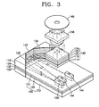
- FIG. 3 is an enlarged perspective view of an optical head for recording and/or reproducing information on an optical or magneto-optical disc according to an embodiment of the present invention.
- the optical head includes a beam input/output coupler 136 formed in an area of a planar waveguide (slab waveguide) 106 having a single mode.
- the beam input/output coupler 136 is shown enlarged for clarity of detail. It is noted that some individual parts such as the beam/output coupler 136 shown in FIG. 3 or other figures of the present disclosure may not be drawn to scale.
- the planar waveguide 106 includes a planar core layer 102 and a lower clad layer 104 that are formed on a portion of a substrate 100, which may be a silica substrate.
- a clad layer 118 is formed on the lower clad layer 104 of the planar waveguide 106. In FIG. 3 , portions of the clad layer 118 are not shown to expose the planar waveguide 106, particularly the lower clad layer 104.
- the clad layer 118, the lower clad layer 104, the planar core layer 102, and the substrate 100 are etched to form beam-shaping mirrors (BSMs) 132 and 134 near the corners of the substrate 100 as shown in FIG. 3 .
- a signal mirror (SM) 142 is formed at a sidewall of the substrate 100.
- the clad layer 118, the lower clad layer 104, the planar core layer 102, and the substrate 100 are etched so that the planar core layer 102 of the planar waveguide 106 is exposed by etching, and then a metal thin film having a high reflectance such as aluminum or gold is filled inside the etched portions.
- the beam input/output coupler 136 is positioned on a portion of the lower clad layer 104 of the planar wave guide layer 106 near the BSMs 132, 134.
- the beam input/output coupler 136 includes a leaky mode directional coupler (LMDC) 114, a hologram beam coupler 116, a PBS 120, a quarter wave plate 122, and an aberration correction (AC) layer 124.
- An objective lens 138 and a disc 140 are positioned on or above the beam input/output coupler 136.
- An LD 130 i.e., a light transmitting element
- PDs 144 i.e., light receiving elements
- the LD 130 transmits a beam in the planar core layer 102 of the planar waveguide 106, and the height of light emitting portion in the LD 130 is preferably equal to the height of the planar core layer 102.
- the LD 130 may be installed in any position for satisfactory transmission of the beam in the planar core layer 102. In other words, a predetermined portion of the planar waveguide 106 may be etched to form the LD 130 in the etched portion, or the LD 130 may be separately installed outside the planar waveguide 106.
- the PDs 144 receive beams guided by the planar core layer 102 of the planar waveguide 106, and the height of light receiving portion in each PD 144 is preferably equal to the height of the planar core layer 102. Similar to the LD 130 installation technique, the PDs 144 may be installed through an etched area of the planar waveguide 106, or alternatively the PDs 144 may be separately installed outside the planar waveguide 106.
- the beam emitted from the LD 130 propagates in the planar core layer 102 of the planar waveguide 106.
- the path of the beam is then corrected by the BSMs 132, 134 positioned as a reflective sidewall as shown in FIG. 3 .
- the beam emitted from the LD 130 and reflected by the BSMs 132, 134 is then "leaked" into the beam input/output coupler 136.
- the beam input/output coupler 136 redirects the propagating beam inside the planar core layer 102 to vertically come out of the planar waveguide 106 through the beam input/output coupler 136 and then to pass through the objective lens 138.
- the beam that has passed through the objective lens 138 is incident on the disc 140 formed parallel to the planar waveguide 106 so as to record (i.e., write) and/or reproduce (i.e., read) information on or from the disc 140.
- the beam reflected off the disc 140 enters the beam input/output coupler 136 and then propagates along the planar core layer 102 of the planar waveguide 106 but now corrected by the SM 142 (instead of the SMs 132, 134) to be received by the PDs 144.
- the beam input/output coupler 136 is formed as an optical thin film compising a plurality of layers that are installed on an area of the planar waveguide 106.
- the thickness of the beam input/output coupler 136 is preferably equal to or less than the total combined thickness of the substrate 100, the planar waveguide 106, and the clad layer 118.
- the thickness of the optical head can be innovatively reduced.
- the characteristics of the planar waveguide or the beam input/output coupler can be controlled so that a light transmitting element is compatible with a blue ray disc (BD) using a blue laser beam having a short wavelength as well as infrared rays or a red laser beam used for a CD or a DVD.
- BD blue ray disc
- an optical head compatible with various types of optical discs can be embodied, and a thickness of the optical head can be remarkably reduced.
- disc devices can be made to be compact.
- FIG. 4 is a plan view illustrating an exemplary path of the propagating beam in the planar waveguide 106 of the optical head
- FIG. 5 is a cross-sectional view illustrating the structure of the beam input/output coupler 136 of the optical head
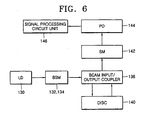
- FIG. 6 is a functional block diagram of the optical head.
- the optical head shown in FIGS. 4-5 includes the planar waveguide 106 comprising the lower clad layer 104, the planar core layer 102, and the substrate 100 (all of which are shown in FIG. 3 ) and has a single mode.
- the LD 130 is a light transmitting element emitting (radiating or transmitting) a beam into the planar waveguide layer 106.
- the PDs 144 are light detecting elements detecting the beams propagating in the planar waveguide layer 106.
- the beam input/output coupler 136 directs the path of the beam leaked into the beam input/output coupler 136 from the planar waveguide layer 106 such that the beam exiting the input/output coupler 136 is substantially perpendicular the planar waveguide layer 106.
- the beam input/output coupler 136 allows the beam reflected off the disc 140 to propagate in the planar waveguide layer 106.
- the beam entering and exiting the input/output coupler 136 is described to be substantially perpendicular to the planar waveguide layer 106; however, non-perpendicular angles of beam path entering and exiting the input/output coupler 136 with respect to the planar waveguide layer 106 is also possible and within the scope of the present disclosure.
- the structure and function of the beam input/output coupler 136 inputting and/or outputting the beam vertically from the ground is described in more detail below.
- the beam emitted by the LD 130 propagates in the planar core layer 102 of the planar waveguide 106 and its path is corrected by the BSMs 132, 134.
- the optical parts such as the BSMs 132 and 134 also provide beam extension function.
- the beam comes out of the planar waveguide 106 through the beam input/output coupler 136 in a direction perpendicular to the direction of the propagating beam in the planar waveguide 106 and then passes it to the objective lens 138.
- the beam passing through the objective lens 138 is incident on the disc 140 (which is parallel to the planar waveguide 106) to write or read information on the disc 140.
- the reflected beam off the disc 140 enters the planar waveguide 106 through the beam input/output coupler 136, as already explained above, for reception by the PDs 144 via the SM 142.
- the beam received by the PDs 144 is then inputted to a signal processing circuit unit 146 (shown in FIG. 6 ).
- the beam input/output coupler 136 as shown in FIG. 4-6 is formed as an optical thin film comprising many layers, and details about the layers, which innovatively contributes to reducing the thickness of the optical head, are described in more detail below.
- the thickness of the beam input/output coupler 136 may be in the range of 100 ⁇ m to 200 ⁇ m.
- the layers of the optical thin film of the beam input/output coupler 136 according to an embodiment of the present invention include the LMDC 114, the hologram beam coupler 116 positioned on the LMDC 114, the PBS 120 positioned on the hologram beam coupler 116, the quarter wave plate 122, and the AC layer 124.
- the LMDC 114 emits a beam proceeding toward the planar waveguide 106 upward at a predetermined angle with the planar waveguide 108 or allows a beam reflected from the disc 140 to be incident on the planar waveguide 106.
- the hologram beam coupler 116 emits the beam having passed through the LMDC 114 vertically from the ground or allows the beam reflected from the disc 140 to be incident on the LMDC 114 at a predetermined angle with the LMDC 114.
- the PBS 120 and the quarter wave plate 122 polarize and pass the beam having passed through the LMDC 114 and the hologram beam coupler 116 and refract the polarized beam that is reflected from the disc 140 and incident on the beam input/output coupler 136 to change a traveling direction of the beam.
- the traveling direction of the beam is changed, the beam is incident on the PDs 144 through the SM 142.
- the AC layer 124 corrects the aberration of the beam input/output coupler 136 formed of multi-layer thin films.
- FIG. 7A is a cross-sectional view of the LMDC 114 and the hologram beam coupler 116 of the beam input/output coupler 136 on the planar waveguide layer 106 of the optical head of an embodiment of the present invention.
- FIG. 7B shows the waveguide refractive index of the LMDC 114.
- FIG. 8 is a table of thicknesses and refractive index differences of layers of the LMDC 114.
- the LMDC 114 includes a leaky core layer 108, an inner clad layer 110, and the upper clad layer 112.
- the present invention as described and shown uses a waveguide mode in which a beam propagates along inside the planar core layer 102 of the planar waveguide 106 and a leaky mode in which a beam propagates through the leaky core layer 108 of the LMDC 114, thereby "leaking" the beam from the planar waveguide layer 106 toward the hologram beam coupler 116 through the LMDC 114, and in the reverse order.
- FIG. 1 the waveguide mode in which a beam propagates along inside the planar core layer 102 of the planar waveguide 106 and a leaky mode in which a beam propagates through the leaky core layer 108 of the LMDC 114, thereby "leaking" the beam from the planar waveguide layer 106 toward the hologram beam coupler 116 through the LMDC 114, and in the reverse order.
- the left part of the cross-sectional view denotes the characteristics of the beam only when the waveguide mode is in operation
- the right part of the cross-section indicates that the characteristics of the beam when the waveguide mode is coupled to the leaky mode.
- the reference numerals 126a through 126d denote the distribution of the beam strength in each layer of the cross-section from the waveguide mode (as in 126a) to the couple wave guide mode and leaky mode (as in 126d).
- the leaky core layer 108 of the LMDC 114 is formed on the planar waveguide 106.
- the planar waveguide 106 includes the substrate 100, the planar core layer 102 that is formed on the substrate 100 and has a refractive index n 2 , and a portion of the lower clad layer 104 having a refractive index n 1 lower than the refractive index n 2 .
- the thicknesses of the planar core layer 102 and the lower clad layer 104 are preferably 2.0 ⁇ m and 1.2 ⁇ m, respectively.
- FIG. 7B shows refractive indexes of the layers constituting the planar waveguide 106 and the layers constituting the LMDC 114.
- n 1 denotes the refractive index of the lower clad layer 104
- n 2 denotes the refractive index of the planar core layer 102
- n 3 denotes the refractive index of the leaky core layer 108
- n 4 denotes the refractive index of an inner clad layer 110
- n 5 denotes the refractive index of the upper clad layer 112.
- the LMDC 114 contacting a portion of the lower clad layer 104 includes:
- ⁇ n denotes the difference between the refractive index of a layer and the refractive index of the substrate 100 having the lowest refractive index.
- ⁇ n of the planar core layer 102 i.e., the refractive index difference between the planar core layer 102 and the substrate 100
- ⁇ n of the leaky core layer 108 i.e., the refractive index difference between the leaky core layer 108 and the substrate 100
- ⁇ n of the lower clad layer is zero meaning that the refractive index of the lower clad layer 104 equals the refractive index of the substrate 100.
- the refractive index of a particular optical material is affected also by the wavelength of the light; therefore, the same material subjected to different light wavelengths may exhibit slightly different refractive indexes.
- the above-mentioned refractive indexes are one set of exemplary values of the shown layers subjected to a blue light having a wavelength of 405 nm.
- the refractive index of the substrate 100 is 1.4702. Nevertheless, it should be noted that the scope of the present invention is not limited to those refractive indexes as shown in FIG. 8 . Other wavelengths of light besides the blue light can be used to produce the same intended results as described and claimed herein without deviating the scope of the present invention.
- a beam emitted by the LD 130 and being propagated in the planar waveguide 106 will leak to the upper clad layer 112 due to the leaky mode formed by the different refractive indexes and the gap existing between the core layers, i.e., between the planar core layer 102 and the leaky core layer 108, as shown in FIGS. 7 and 8 .
- the leaky mode is formed. Under this leaky mode condition, the beams propagating in the planar core layer 102 of the planar waveguide 106 will leak to the LMCD 114.
- the beams propagating in the planar core layer 102 will pass through the lower clad layer 104 and will be incident on the LMDC 114, because the refractive index of the lower clad layer 104 is lower than the refractive index of the core layer 102.
- the beams are able to propagate through the leaky core layer 108. Since the refractive index of the inner clad layer 110 is low, the beams coupled and proceeding toward the leaky core layer 108 are leaked toward the upper clad layer 112 at a predetermined angle.
- the LMDC 114 controls the refractive index of the upper clad layer 112 to control an amount and an angle of the beam propagated to the upper clad layer 112 and controls the thickness of the inner clad layer 110 to control coupling efficiency and a coupling length.
- the LMDC 114 has a leaky beam having a maximum leaky effect and a Gaussian distribution within a range of (b-L/2) ⁇ Y ⁇ (b+L/2), where b denotes a distance from a beam input to the LMDC 114 to the center of the LMDC 114, L denotes a diameter of the LMDC 114, and Y denotes both ends of the LMDC 114.
- the beam incident on the planar core layer 102 of the planar waveguide 106 by the LD 130 proceeds from the left toward the right and then is incident on a starting point b-L/2 of the LMDC 114.
- the thickness of the lower clad layer 104 is controlled to sufficiently transmit a power from the waveguide mode toward the leaky mode so that a power of the waveguide mode is vanished at an ending side "b+L/2" of the planar waveguide 106.
- the power transmitted from the waveguide mode toward the leaky mode generates a leaky beam, maintaining a predetermined angle.
- the leaky beam is refracted by the hologram beam coupler 116 to proceed in a vertical direction so as to be transmitted toward the disc 140.
- FIG. 9 is a graph illustrating the power-transmitting characteristics of the LMDC 114.
- the distribution of an input beam propagated toward a hologram beam coupler may be formed in the form of Gaussian function.
- Beam loss of a leaky mode is reduced in index number along a direction toward which a beam proceeds as marked with reference numeral 203.
- Beam coupling toward the leaky mode is accumulated and increased along the direction toward which the beam proceeds as marked with reference numeral 201.
- a power distribution of a leaky beam that is a product of the beam loss and the beam coupling may be formed in the form of the Gaussian function as marked with reference numeral 205.
- Reference numeral 203 denotes a power of the leaky mode reduced along the direction toward which the beam proceeds
- reference numeral 201 denotes the power of the leaky mode accumulated along the direction
- reference numeral 205 denotes a power distribution of the leaky beam propagated to a hologram beam coupler.
- the optical parts necessary for forming the beams can be made of thin films on the planar waveguide.
- the thicknesses of the optical parts are limited to a thickness of a waveguide.
- a thickness of the optical head can be innovatively reduced.
- individual optical parts necessary for the optical head are integrated on the planar waveguide having a single mode so as to be formed as individual bodies.
- the thickness of the optical head can be reduced.
- the characteristics of the planar waveguide or the beam input/output coupler can be controlled so that a light transmitting element is compatible with a BD using a blue laser beam having a short wavelength as well as infrared rays or a red laser beam used for a CD or a DVD.
- the optical head can be compatible with various types of discs.
- the thickness of the optical head can be remarkably reduced. As a result, disc devices can be made compact.
Landscapes
- Physics & Mathematics (AREA)
- Optics & Photonics (AREA)
- Optical Head (AREA)
- Optical Integrated Circuits (AREA)
- Optical Couplings Of Light Guides (AREA)
Claims (19)
- Optischer Kopf, umfassend:ein Licht emittierendes Element (130), das einen Lichtstrahl emittiert;einen planaren Wellenleiter (106), der auf einem Substrat gebildet ist und den Strahl empfängt, der von dem Licht emittierenden Element (130) emittiert wird;einen Strahleingangs-/Strahlausgangskoppler (136), der eine Vielzahl von Dünnschichten aufweist, die auf einem Abschnitt des planaren Wellenleiters (106) gebildet sind;eine optische Platte (140), die über dem Strahleingangs-/Strahlausgangskoppler (136) gebildet ist;
wobei der Strahleingangs-/Strahlausgangskoppler (136) den Strahl von dem planaren Wellenleiter (106) empfängt und den Strahl in einem Winkel auf die Platte (140) überträgt; und
wobei der Strahleingangs-/Strahlausgangskoppler (136) den von der Platte (140) reflektierten Strahl empfängt und den reflektierten Strahl in den planaren Wellenleiter (106) überträgt; undein Licht empfangendes Element (144), das den reflektierten Strahl empfängt, der durch den Strahleingangs-/Strahlausgangskoppler (136) hindurch in den planaren Wellenleiter (106) übertragen wird,
dadurch gekennzeichnet, dass der Strahleingangs-/Strahlausgangskoppler (136) folgendes umfasst:einen Leckwellen-Richtungskoppler (114);einen Hologramm-Strahlkoppler (116), der auf dem Leckwellen-Richtungskoppler (114) gebildet ist;einen polarisierten Strahlteiler (120), der auf dem Hologramm-Strahlkoppler (116) gebildet ist; undeine Viertelwellenplatte (122), die auf dem polarisierten Strahlteiler (120) gebildet ist. - Optischer Kopf nach Anspruch 1, ferner umfassend einen Strahlformungsspiegel (132, 134), der in einem Abschnitt des planaren Wellenleiters (106) als reflektierende Seitenwand gebildet ist, um den Weg des Strahls zu ändern, der von dem Licht emittierenden Element (130) emittiert wird und sich in dem planaren Wellenleiter (106) ausbreitet.
- Optischer Kopf nach Anspruch 1, ferner umfassend einen Signalspiegel (142), der in einem Abschnitt des planaren Wellenleiters (106) als reflektierende Seitenwand gebildet wird, um den Weg des reflektierten Strahls in dem planaren Wellenleiter (106) zu ändern, wobei der reflektierte Strahl der Strahl ist, der von der Platte (140) reflektiert wird und in den planaren Wellenleiter (106) durch den Strahleingangs-/Strahlausgangskoppler (136) hindurch übertragen wird.
- Optischer Kopf nach Anspruch 1, wobei der Strahleingangs-/Strahlausgangskoppler (136) ferner eine Aberrationskorrekturschicht (124) umfasst, die auf der viertelwellenplatte (122) gebildet ist.
- Optischer Kopf nach Anspruch 1, wobei der Leckwellen-Richtungskoppler (114) eine Leckwellen-Kernschicht (108) umfasst, die auf dem planaren Wellenleiter (106) gebildet ist.
- Optischer Kopf nach Anspruch 1, wobei der planare Wellenleiter (106) folgendes umfasst:eine planare Kernschicht (102), die eine Brechungszahl n2 aufweist und auf dem Substrat gebildet ist; undeine untere Mantelschicht (104), die eine Brechungszahl n1 aufweist und auf der planaren Kernschicht (102) gebildet ist, wobei n2 > n1.
- Optischer Kopf nach Anspruch 6, wobei der Leckwellen-Richtungskoppler (114) folgendes umfasst:eine Leckwellen-Kernschicht (108), die eine Brechungszahl n3 aufweist und auf der unteren Mantelschicht (104) gebildet ist;eine innere Mantelschicht (110), die eine Brechungszahl n4 aufweist und auf der Leckwellen-Kernschicht (108) gebildet ist; undeine obere Mantelschicht (112), die eine Brechungszahl n5 aufweist und auf der inneren Mantelschicht (110) gebildet ist;wobei n5 > n4 > n3 > n2 > n1, um eine Leckwelle in dem Leckwellen-Richtungskoppler (114) zu bilden, so dass der Strahl, der sich in dem planaren Wellenleiter (106) ausbreitet, in den Leckwellen-Richtungskoppler (114) durchgelassen wird.
- Optischer Kopf nach Anspruch 1, wobei die Richtung des Strahls, der von dem Eingangs-/Ausgangskoppler (136) auf die optische Platte (140) übertragen wird, zu dem planaren Wellenleiter (106) ungefähr rechtwinklig ist, und
wobei die Richtung des Strahls, der von der Platte (140) reflektiert und in den planaren Wellenleiter (106) übertragen wird, zu dem planaren Wellenleiter (106) ungefähr rechtwinklig ist. - Optischer Kopf nach Anspruch 1, wobei der Hologramm-Strahlkoppler (116) den Strahl, der in den Leckwellen-Richtungskoppler (114) durchgelassen wird, in einer senkrechten Richtung überträgt; und
wobei der Hologramm-Strahlkoppler (116) den Strahl, der von der Platte (140) aus reflektiert wird, auf den Leckwellen-Richtungskoppler (114) in einem vorherbestimmten Winkel auffallen lässt. - Optischer Kopf nach Anspruch 1, wobei der polarisierte Strahlteiler (120) und die Viertelwellenplatte (122) den Strahl, der durch den Leckwellen-Richtungskoppler (114) und den Hologramm-Strahlkoppler (116) hindurch gegangen ist, polarisieren und durchlassen; und
wobei der polarisierte Strahlteiler (120) und die Viertelwellenplatte (122) den Strahl polarisieren, der von der Platte (140) reflektiert wird, um eine Richtung des Strahls zu ändern, um den Strahl an das Licht empfangende Element (144) zu übertragen. - Optischer Kopf nach Anspruch 4, wobei die Aberrationskorrekturschicht (124), die auf der Viertelwellenplatte (122) installiert ist, die Aberration des Strahleingangs-/Strahlausgangskoppler (136) korrigiert, der mehrlagige Dünnschichten umfasst.
- Optischer Kopf, umfassend:ein Licht emittierendes Element (130), das einen Lichtstrahl emittiert;einen planaren Wellenleiter (106), der auf einem Substrat gebildet ist und den Strahl empfängt, der von dem Licht emittierenden Element (130) emittiert wird;einen Strahlformungsspiegel (132, 134), der in einem Abschnitt des planaren Wellenleiters (106) als reflektierende Seitenwand gebildet ist, um den Weg des Strahls zu ändern, der von dem Licht emittierenden Element (130) emittiert wird und sich in dem planaren Wellenleiter (106) ausbreitet;einen Strahleingangs-/Strahlausgangskoppler (136), der eine Vielzahl von Dünnschichten aufweist, die in einem Abschnitt des planaren Wellenleiters (106) gebildet sind;
wobei der Strahleingangs-/Strahlausgangskoppler (136) den Strahl aus dem Strahlformungsspiegel (132, 134) empfängt und den Strahl in einer Richtung überträgt, die zu dem planaren Wellenleiter (106) im Wesentlichen senkrecht ist, in Richtung auf eine Platte (140), die über dem planaren Wellenleiter (106) positioniert ist, um Informationen auf der Platte (140) aufzuzeichnen und/oder davon wiederzugeben (abzulesen); und
wobei der Strahleingangs-/Strahlausgangskoppler (136) den von der Platte (140) aus reflektierten Strahl in den planaren Wellenleiter (106) überträgt;einen Signalspiegel (142), der in einem Abschnitt des planaren Wellenleiters (106) als reflektierende Seitenwand gebildet ist, um den Weg des Strahls zu ändern, der von der Platte (140) reflektiert wird und in den planaren Wellenleiter (106) übertragen wird;ein Licht empfangendes Element (144), das den Strahl empfängt, der von dem Signalspiegel (142) aus reflektiert wird; undeine Signalverarbeitungs-Schaltungseinheit (146) für die Signalverarbeitung des Strahls, der von dem Licht empfangenden Element (144) empfangen wird,
dadurch gekennzeichnet, dass der Strahleingangs-/Strahlausgangskoppler (136) folgendes umfasst:einen Leckwellen-Richtungskoppler (114);einen Hologramm-Strahlkoppler (116), der auf dem Leckwellen-Richtungskoppler (114) gebildet ist;einen polarisierten Strahlteiler (120), der auf dem Hologramm-Strahlkoppler (116) gebildet ist; undeine Viertelwellenplatte (122), die auf dem polarisierten Strahlteiler (120) gebildet ist. - Optischer Kopf nach Anspruch 12, wobei der Strahleingangs-/Strahlausgangskoppler (136) ferner eine Aberrationskorrekturschicht (124) umfasst, die auf der Viertelwellenplatte (122) gebildet ist.
- Optischer Kopf nach Anspruch 13, wobei der Leckwellen-Richtungskoppler (114) eine Leckwellen-Kernschicht (108) umfasst, die auf dem planaren Wellenleiter (106) gebildet ist,
wobei die Leckwellen-Kernschicht (108) den Strahl emittiert, der sich in dem planaren Wellenleiter (106) nach oben in einem vorherbestimmten Winkel gemäß einer Leckwelle ausbreitet, oder
wobei die Leckwellen-Kernschicht (108) den Strahl, der von der Platte (140) aus reflektiert wird, auf den planaren Wellenleiter (106) einfallen lässt. - Optischer Kopf nach Anspruch 12, wobei der planare Wellenleiter (106) folgendes umfasst:eine planare Kernschicht (102), die eine Brechungszahl n2 aufweist und auf dem Substrat gebildet ist; undeine untere Mantelschicht (104), die eine Brechungszahl n1 aufweist und auf der planaren Kernschicht (102) gebildet ist, wobei n2 > n1.
- Optischer Kopf nach Anspruch 15, wobei der Leckwellen-Richtungskoppler (114) folgendes umfasst:eine Leckwellen-Kernschicht (108), die eine Brechungszahl n3 aufweist und auf der unteren Mantelschicht (104) gebildet ist;eine innere Mantelschicht (110), die eine Brechungszahl n4 aufweist und auf der Leckwellen-Kernschicht (108) gebildet ist; undeine obere Mantelschicht (112), die eine Brechungszahl n5 aufweist und auf der inneren Mantelschicht (110) gebildet ist,wobei n5 > n4 > n3 > n2 > n1, um eine Leckwelle in dem Leckwellen-Richtungskoppler (114) zu bilden, so dass der Strahl, der sich in dem planaren Wellenleiter (106) ausbreitet, in den Leckwellen-Richtungskoppler (114) durchgelassen wird.
- Optischer Kopf nach Anspruch 12, wobei entweder das Licht emittierende Element (130) oder das Licht empfangende Element (144) in einem geätzten Abschnitt des planaren Lichtwellenleiters (106) gebildet ist.
- Optischer Kopf nach Anspruch 17, wobei die Höhe entweder eines Licht emittierenden Abschnitts in dem Licht emittierenden Element (130) oder eines Licht empfangenden Abschnitts in dem Licht empfangenden Element (144) gleich der Höhe des planaren Wellenleiters (106) ist.
- Optischer Kopf nach Anspruch 18, wobei das Licht emittierende Element (130) eine Laserdiode umfasst, und wobei das Licht empfangende Element (144) eine Photodiode umfasst.
Applications Claiming Priority (2)
| Application Number | Priority Date | Filing Date | Title |
|---|---|---|---|
| KR20040103073 | 2004-12-08 | ||
| KR1020050053053A KR100701122B1 (ko) | 2004-12-08 | 2005-06-20 | 평면 도파로 상에 빔 입출사 커플러를 갖는 광 헤드 |
Publications (3)
| Publication Number | Publication Date |
|---|---|
| EP1669987A2 EP1669987A2 (de) | 2006-06-14 |
| EP1669987A3 EP1669987A3 (de) | 2009-01-14 |
| EP1669987B1 true EP1669987B1 (de) | 2010-03-31 |
Family
ID=36051488
Family Applications (1)
| Application Number | Title | Priority Date | Filing Date |
|---|---|---|---|
| EP05257138A Expired - Lifetime EP1669987B1 (de) | 2004-12-08 | 2005-11-21 | Optischer Kopf mit Strahleneingangs-/ausgangskoppler auf einem planaren Wellenleiter |
Country Status (3)
| Country | Link |
|---|---|
| US (1) | US7580336B2 (de) |
| EP (1) | EP1669987B1 (de) |
| JP (1) | JP4096004B2 (de) |
Families Citing this family (4)
| Publication number | Priority date | Publication date | Assignee | Title |
|---|---|---|---|---|
| JP2008089778A (ja) * | 2006-09-29 | 2008-04-17 | Sumitomo Osaka Cement Co Ltd | 光デバイスおよび光デバイスの製造方法 |
| JP5094636B2 (ja) * | 2008-08-25 | 2012-12-12 | 新光電気工業株式会社 | 光電気配線用パッケージ |
| US8791405B2 (en) * | 2009-12-03 | 2014-07-29 | Samsung Electronics Co., Ltd. | Optical waveguide and coupler apparatus and method of manufacturing the same |
| US11448815B2 (en) * | 2020-11-06 | 2022-09-20 | Meta Platforms Technologies LLC | Slab waveguide and projector with intermodal coupling |
Family Cites Families (15)
| Publication number | Priority date | Publication date | Assignee | Title |
|---|---|---|---|---|
| US4737946A (en) * | 1984-09-03 | 1988-04-12 | Omron Tateisi Electronics Co. | Device for processing optical data with improved optical allignment means |
| JPS61248245A (ja) | 1985-04-25 | 1986-11-05 | Mitsubishi Electric Corp | 光学式ヘツド装置 |
| JPS6289250A (ja) * | 1985-10-16 | 1987-04-23 | Fuji Photo Film Co Ltd | 光デイスク用ピツクアツプ |
| EP0226647B1 (de) * | 1985-12-17 | 1991-05-29 | Ibm Deutschland Gmbh | Schreib/Lesekopf für optische Platten |
| JPS63164033A (ja) | 1986-12-26 | 1988-07-07 | Matsushita Electric Ind Co Ltd | 光ピツクアツプ装置 |
| JP2539406B2 (ja) * | 1987-02-04 | 1996-10-02 | 株式会社日立製作所 | 固体光ピツクアツプ |
| US5070488A (en) | 1988-06-29 | 1991-12-03 | Atsuko Fukushima | Optical integrated circuit and optical apparatus |
| EP0360209A3 (de) | 1988-09-19 | 1992-08-19 | Hitachi, Ltd. | Optischer Kopf und optisches Datenverarbeitungsgerät |
| JPH04219657A (ja) * | 1990-04-13 | 1992-08-10 | Ricoh Co Ltd | 光磁気情報記録再生装置及びモードスプリッタ |
| US5166989A (en) * | 1990-11-16 | 1992-11-24 | International Business Machines Corporation | Integrated polarization detection system |
| JP2716000B2 (ja) * | 1995-06-23 | 1998-02-18 | 日本電気株式会社 | 光ヘッド |
| WO1999031658A1 (en) | 1997-12-16 | 1999-06-24 | Daewoo Electronics Co., Ltd. | Integrated optical pickup system for use with optical disks of different thicknesses |
| US7079472B2 (en) | 1999-06-23 | 2006-07-18 | Dphi Acquisitions, Inc. | Beamshaper for optical head |
| KR100480786B1 (ko) | 2002-09-02 | 2005-04-07 | 삼성전자주식회사 | 커플러를 가지는 집적형 광 헤드 |
| KR100518030B1 (ko) * | 2003-07-08 | 2005-10-04 | 한국전자통신연구원 | 누설모드를 이용한 고 효율 광 커플러 |
-
2005
- 2005-11-10 US US11/270,998 patent/US7580336B2/en not_active Expired - Fee Related
- 2005-11-21 EP EP05257138A patent/EP1669987B1/de not_active Expired - Lifetime
- 2005-12-07 JP JP2005353998A patent/JP4096004B2/ja not_active Expired - Fee Related
Also Published As
| Publication number | Publication date |
|---|---|
| US7580336B2 (en) | 2009-08-25 |
| EP1669987A2 (de) | 2006-06-14 |
| JP2006164504A (ja) | 2006-06-22 |
| EP1669987A3 (de) | 2009-01-14 |
| US20060120249A1 (en) | 2006-06-08 |
| JP4096004B2 (ja) | 2008-06-04 |
Similar Documents
| Publication | Publication Date | Title |
|---|---|---|
| US7088664B2 (en) | Reflection type compound prism and optical pickup apparatus employing the same | |
| KR100480786B1 (ko) | 커플러를 가지는 집적형 광 헤드 | |
| US7457206B2 (en) | Optical head, optical information storage apparatus, and their fabrication method | |
| US20040246874A1 (en) | Hologram coupled member and method for manufacturing the same, and hologram laser unit and optical pickup apparatus | |
| KR100765741B1 (ko) | 일 매의 렌즈로 된 고개구수의 대물렌즈 및 이를 채용한광픽업장치 | |
| US5418765A (en) | Apparatus for recording and reproducing optical information having an optical waveguide | |
| US6519379B1 (en) | Optical integrated device and manufacturing method thereof | |
| US6896419B2 (en) | Optical pickup | |
| EP1669987B1 (de) | Optischer Kopf mit Strahleneingangs-/ausgangskoppler auf einem planaren Wellenleiter | |
| KR100813945B1 (ko) | 광픽업장치 및 이에 적용되는 기록매체 | |
| US6639887B1 (en) | Optical apparatus with laser light receiver and focus error generator in the same layer | |
| US6408116B1 (en) | Light guide path element and optical pickup | |
| KR100701122B1 (ko) | 평면 도파로 상에 빔 입출사 커플러를 갖는 광 헤드 | |
| EP1624453A1 (de) | Optischer kopf und optisches plattenlaufwerk | |
| JP2000222769A (ja) | 光導波路素子及び光ピックアップ | |
| JP3152456B2 (ja) | 焦点誤差信号検出装置及び光情報記録再生装置並びに光磁気情報記録再生装置 | |
| JP2000215503A (ja) | 光集積装置 | |
| KR100403596B1 (ko) | 직각삼각형 모양의 빔스프리터를 구비한 광픽업장치와이를 이용한 광축보정방법 | |
| JP2004005903A (ja) | 光ピックアップ装置および光ディスク装置 | |
| US20050237903A1 (en) | Optical pickup head compatible with two different optical recording media | |
| JPH11232685A (ja) | ビーム整形素子およびそれを用いた光ピックアップ | |
| JP2004005945A (ja) | 光ピックアップ装置および光ディスク装置 | |
| JPH03168938A (ja) | 導波路型光学ヘッド | |
| JPS63222342A (ja) | 光ヘツド装置 | |
| JPH0763949A (ja) | 光計測装置 |
Legal Events
| Date | Code | Title | Description |
|---|---|---|---|
| PUAI | Public reference made under article 153(3) epc to a published international application that has entered the european phase |
Free format text: ORIGINAL CODE: 0009012 |
|
| 17P | Request for examination filed |
Effective date: 20051208 |
|
| AK | Designated contracting states |
Kind code of ref document: A2 Designated state(s): AT BE BG CH CY CZ DE DK EE ES FI FR GB GR HU IE IS IT LI LT LU LV MC NL PL PT RO SE SI SK TR |
|
| AX | Request for extension of the european patent |
Extension state: AL BA HR MK YU |
|
| PUAL | Search report despatched |
Free format text: ORIGINAL CODE: 0009013 |
|
| AK | Designated contracting states |
Kind code of ref document: A3 Designated state(s): AT BE BG CH CY CZ DE DK EE ES FI FR GB GR HU IE IS IT LI LT LU LV MC NL PL PT RO SE SI SK TR |
|
| AX | Request for extension of the european patent |
Extension state: AL BA HR MK YU |
|
| 17Q | First examination report despatched |
Effective date: 20090223 |
|
| AKX | Designation fees paid |
Designated state(s): AT BE BG CH CY CZ DE DK EE ES FI FR GB GR HU IE IS IT LI LT LU LV MC NL PL PT RO SE SI SK TR |
|
| GRAP | Despatch of communication of intention to grant a patent |
Free format text: ORIGINAL CODE: EPIDOSNIGR1 |
|
| GRAS | Grant fee paid |
Free format text: ORIGINAL CODE: EPIDOSNIGR3 |
|
| GRAA | (expected) grant |
Free format text: ORIGINAL CODE: 0009210 |
|
| AK | Designated contracting states |
Kind code of ref document: B1 Designated state(s): AT BE BG CH CY CZ DE DK EE ES FI FR GB GR HU IE IS IT LI LT LU LV MC NL PL PT RO SE SI SK TR |
|
| REG | Reference to a national code |
Ref country code: GB Ref legal event code: FG4D Ref country code: CH Ref legal event code: EP |
|
| REG | Reference to a national code |
Ref country code: IE Ref legal event code: FG4D |
|
| REF | Corresponds to: |
Ref document number: 602005020240 Country of ref document: DE Date of ref document: 20100512 Kind code of ref document: P |
|
| REG | Reference to a national code |
Ref country code: NL Ref legal event code: VDEP Effective date: 20100331 |
|
| PG25 | Lapsed in a contracting state [announced via postgrant information from national office to epo] |
Ref country code: LT Free format text: LAPSE BECAUSE OF FAILURE TO SUBMIT A TRANSLATION OF THE DESCRIPTION OR TO PAY THE FEE WITHIN THE PRESCRIBED TIME-LIMIT Effective date: 20100331 |
|
| LTIE | Lt: invalidation of european patent or patent extension |
Effective date: 20100331 |
|
| PG25 | Lapsed in a contracting state [announced via postgrant information from national office to epo] |
Ref country code: LV Free format text: LAPSE BECAUSE OF FAILURE TO SUBMIT A TRANSLATION OF THE DESCRIPTION OR TO PAY THE FEE WITHIN THE PRESCRIBED TIME-LIMIT Effective date: 20100331 Ref country code: PL Free format text: LAPSE BECAUSE OF FAILURE TO SUBMIT A TRANSLATION OF THE DESCRIPTION OR TO PAY THE FEE WITHIN THE PRESCRIBED TIME-LIMIT Effective date: 20100331 Ref country code: SI Free format text: LAPSE BECAUSE OF FAILURE TO SUBMIT A TRANSLATION OF THE DESCRIPTION OR TO PAY THE FEE WITHIN THE PRESCRIBED TIME-LIMIT Effective date: 20100331 Ref country code: AT Free format text: LAPSE BECAUSE OF FAILURE TO SUBMIT A TRANSLATION OF THE DESCRIPTION OR TO PAY THE FEE WITHIN THE PRESCRIBED TIME-LIMIT Effective date: 20100331 Ref country code: FI Free format text: LAPSE BECAUSE OF FAILURE TO SUBMIT A TRANSLATION OF THE DESCRIPTION OR TO PAY THE FEE WITHIN THE PRESCRIBED TIME-LIMIT Effective date: 20100331 |
|
| PG25 | Lapsed in a contracting state [announced via postgrant information from national office to epo] |
Ref country code: ES Free format text: LAPSE BECAUSE OF FAILURE TO SUBMIT A TRANSLATION OF THE DESCRIPTION OR TO PAY THE FEE WITHIN THE PRESCRIBED TIME-LIMIT Effective date: 20100712 Ref country code: NL Free format text: LAPSE BECAUSE OF FAILURE TO SUBMIT A TRANSLATION OF THE DESCRIPTION OR TO PAY THE FEE WITHIN THE PRESCRIBED TIME-LIMIT Effective date: 20100331 Ref country code: RO Free format text: LAPSE BECAUSE OF FAILURE TO SUBMIT A TRANSLATION OF THE DESCRIPTION OR TO PAY THE FEE WITHIN THE PRESCRIBED TIME-LIMIT Effective date: 20100331 Ref country code: SE Free format text: LAPSE BECAUSE OF FAILURE TO SUBMIT A TRANSLATION OF THE DESCRIPTION OR TO PAY THE FEE WITHIN THE PRESCRIBED TIME-LIMIT Effective date: 20100331 Ref country code: CY Free format text: LAPSE BECAUSE OF FAILURE TO SUBMIT A TRANSLATION OF THE DESCRIPTION OR TO PAY THE FEE WITHIN THE PRESCRIBED TIME-LIMIT Effective date: 20100331 Ref country code: EE Free format text: LAPSE BECAUSE OF FAILURE TO SUBMIT A TRANSLATION OF THE DESCRIPTION OR TO PAY THE FEE WITHIN THE PRESCRIBED TIME-LIMIT Effective date: 20100331 |
|
| PG25 | Lapsed in a contracting state [announced via postgrant information from national office to epo] |
Ref country code: IS Free format text: LAPSE BECAUSE OF FAILURE TO SUBMIT A TRANSLATION OF THE DESCRIPTION OR TO PAY THE FEE WITHIN THE PRESCRIBED TIME-LIMIT Effective date: 20100731 Ref country code: CZ Free format text: LAPSE BECAUSE OF FAILURE TO SUBMIT A TRANSLATION OF THE DESCRIPTION OR TO PAY THE FEE WITHIN THE PRESCRIBED TIME-LIMIT Effective date: 20100331 Ref country code: SK Free format text: LAPSE BECAUSE OF FAILURE TO SUBMIT A TRANSLATION OF THE DESCRIPTION OR TO PAY THE FEE WITHIN THE PRESCRIBED TIME-LIMIT Effective date: 20100331 |
|
| PG25 | Lapsed in a contracting state [announced via postgrant information from national office to epo] |
Ref country code: DK Free format text: LAPSE BECAUSE OF FAILURE TO SUBMIT A TRANSLATION OF THE DESCRIPTION OR TO PAY THE FEE WITHIN THE PRESCRIBED TIME-LIMIT Effective date: 20100331 |
|
| PLBE | No opposition filed within time limit |
Free format text: ORIGINAL CODE: 0009261 |
|
| STAA | Information on the status of an ep patent application or granted ep patent |
Free format text: STATUS: NO OPPOSITION FILED WITHIN TIME LIMIT |
|
| 26N | No opposition filed |
Effective date: 20110104 |
|
| PG25 | Lapsed in a contracting state [announced via postgrant information from national office to epo] |
Ref country code: IT Free format text: LAPSE BECAUSE OF FAILURE TO SUBMIT A TRANSLATION OF THE DESCRIPTION OR TO PAY THE FEE WITHIN THE PRESCRIBED TIME-LIMIT Effective date: 20100331 |
|
| PG25 | Lapsed in a contracting state [announced via postgrant information from national office to epo] |
Ref country code: MC Free format text: LAPSE BECAUSE OF NON-PAYMENT OF DUE FEES Effective date: 20101130 |
|
| REG | Reference to a national code |
Ref country code: CH Ref legal event code: PL |
|
| PG25 | Lapsed in a contracting state [announced via postgrant information from national office to epo] |
Ref country code: CH Free format text: LAPSE BECAUSE OF NON-PAYMENT OF DUE FEES Effective date: 20101130 Ref country code: LI Free format text: LAPSE BECAUSE OF NON-PAYMENT OF DUE FEES Effective date: 20101130 |
|
| REG | Reference to a national code |
Ref country code: FR Ref legal event code: ST Effective date: 20110801 |
|
| REG | Reference to a national code |
Ref country code: DE Ref legal event code: R119 Ref document number: 602005020240 Country of ref document: DE Effective date: 20110601 Ref country code: DE Ref legal event code: R119 Ref document number: 602005020240 Country of ref document: DE Effective date: 20110531 |
|
| PG25 | Lapsed in a contracting state [announced via postgrant information from national office to epo] |
Ref country code: IE Free format text: LAPSE BECAUSE OF NON-PAYMENT OF DUE FEES Effective date: 20101121 Ref country code: FR Free format text: LAPSE BECAUSE OF NON-PAYMENT OF DUE FEES Effective date: 20101130 |
|
| PGFP | Annual fee paid to national office [announced via postgrant information from national office to epo] |
Ref country code: BE Payment date: 20111107 Year of fee payment: 7 |
|
| PG25 | Lapsed in a contracting state [announced via postgrant information from national office to epo] |
Ref country code: HU Free format text: LAPSE BECAUSE OF FAILURE TO SUBMIT A TRANSLATION OF THE DESCRIPTION OR TO PAY THE FEE WITHIN THE PRESCRIBED TIME-LIMIT Effective date: 20101001 Ref country code: BG Free format text: LAPSE BECAUSE OF FAILURE TO SUBMIT A TRANSLATION OF THE DESCRIPTION OR TO PAY THE FEE WITHIN THE PRESCRIBED TIME-LIMIT Effective date: 20100331 Ref country code: LU Free format text: LAPSE BECAUSE OF NON-PAYMENT OF DUE FEES Effective date: 20101121 |
|
| PG25 | Lapsed in a contracting state [announced via postgrant information from national office to epo] |
Ref country code: TR Free format text: LAPSE BECAUSE OF FAILURE TO SUBMIT A TRANSLATION OF THE DESCRIPTION OR TO PAY THE FEE WITHIN THE PRESCRIBED TIME-LIMIT Effective date: 20100331 |
|
| BERE | Be: lapsed |
Owner name: ELECTRONICS AND TELECOMMUNICATIONS RESEARCH INSTI Effective date: 20121130 |
|
| PG25 | Lapsed in a contracting state [announced via postgrant information from national office to epo] |
Ref country code: PT Free format text: LAPSE BECAUSE OF NON-PAYMENT OF DUE FEES Effective date: 20100331 |
|
| PG25 | Lapsed in a contracting state [announced via postgrant information from national office to epo] |
Ref country code: BE Free format text: LAPSE BECAUSE OF NON-PAYMENT OF DUE FEES Effective date: 20121130 |
|
| PG25 | Lapsed in a contracting state [announced via postgrant information from national office to epo] |
Ref country code: BG Free format text: LAPSE BECAUSE OF FAILURE TO SUBMIT A TRANSLATION OF THE DESCRIPTION OR TO PAY THE FEE WITHIN THE PRESCRIBED TIME-LIMIT Effective date: 20100630 |
|
| PG25 | Lapsed in a contracting state [announced via postgrant information from national office to epo] |
Ref country code: GR Free format text: LAPSE BECAUSE OF FAILURE TO SUBMIT A TRANSLATION OF THE DESCRIPTION OR TO PAY THE FEE WITHIN THE PRESCRIBED TIME-LIMIT Effective date: 20100331 |
|
| PG25 | Lapsed in a contracting state [announced via postgrant information from national office to epo] |
Ref country code: DE Free format text: LAPSE BECAUSE OF FAILURE TO SUBMIT A TRANSLATION OF THE DESCRIPTION OR TO PAY THE FEE WITHIN THE PRESCRIBED TIME-LIMIT Effective date: 20110531 |
|
| PGFP | Annual fee paid to national office [announced via postgrant information from national office to epo] |
Ref country code: GB Payment date: 20141021 Year of fee payment: 10 |
|
| GBPC | Gb: european patent ceased through non-payment of renewal fee |
Effective date: 20151121 |
|
| PG25 | Lapsed in a contracting state [announced via postgrant information from national office to epo] |
Ref country code: GB Free format text: LAPSE BECAUSE OF NON-PAYMENT OF DUE FEES Effective date: 20151121 |