US20060120249A1 - Optical head having a beam input/output coupler on a planar waveguide - Google Patents
Optical head having a beam input/output coupler on a planar waveguide Download PDFInfo
- Publication number
- US20060120249A1 US20060120249A1 US11/270,998 US27099805A US2006120249A1 US 20060120249 A1 US20060120249 A1 US 20060120249A1 US 27099805 A US27099805 A US 27099805A US 2006120249 A1 US2006120249 A1 US 2006120249A1
- Authority
- US
- United States
- Prior art keywords
- planar waveguide
- optical head
- coupler
- leaky
- disc
- Prior art date
- Legal status (The legal status is an assumption and is not a legal conclusion. Google has not performed a legal analysis and makes no representation as to the accuracy of the status listed.)
- Granted
Links
- 230000003287 optical effect Effects 0.000 title claims abstract description 105
- 239000000758 substrate Substances 0.000 claims abstract description 28
- 239000010409 thin film Substances 0.000 claims abstract description 12
- 239000010410 layer Substances 0.000 claims description 95
- 239000012792 core layer Substances 0.000 claims description 52
- 230000001902 propagating effect Effects 0.000 claims description 11
- 230000004075 alteration Effects 0.000 claims description 6
- 230000008859 change Effects 0.000 claims description 6
- 238000007493 shaping process Methods 0.000 claims description 5
- 230000000644 propagated effect Effects 0.000 abstract description 7
- 230000008878 coupling Effects 0.000 description 4
- 238000010168 coupling process Methods 0.000 description 4
- 238000005859 coupling reaction Methods 0.000 description 4
- NCGICGYLBXGBGN-UHFFFAOYSA-N 3-morpholin-4-yl-1-oxa-3-azonia-2-azanidacyclopent-3-en-5-imine;hydrochloride Chemical compound Cl.[N-]1OC(=N)C=[N+]1N1CCOCC1 NCGICGYLBXGBGN-UHFFFAOYSA-N 0.000 description 3
- 241001025261 Neoraja caerulea Species 0.000 description 3
- VYPSYNLAJGMNEJ-UHFFFAOYSA-N Silicium dioxide Chemical compound O=[Si]=O VYPSYNLAJGMNEJ-UHFFFAOYSA-N 0.000 description 2
- 230000008901 benefit Effects 0.000 description 2
- 238000010586 diagram Methods 0.000 description 2
- 239000000463 material Substances 0.000 description 2
- 230000009467 reduction Effects 0.000 description 2
- 235000005811 Viola adunca Nutrition 0.000 description 1
- 240000009038 Viola odorata Species 0.000 description 1
- 235000013487 Viola odorata Nutrition 0.000 description 1
- 235000002254 Viola papilionacea Nutrition 0.000 description 1
- 229910052782 aluminium Inorganic materials 0.000 description 1
- XAGFODPZIPBFFR-UHFFFAOYSA-N aluminium Chemical compound [Al] XAGFODPZIPBFFR-UHFFFAOYSA-N 0.000 description 1
- 230000005540 biological transmission Effects 0.000 description 1
- 230000000694 effects Effects 0.000 description 1
- 238000005530 etching Methods 0.000 description 1
- PCHJSUWPFVWCPO-UHFFFAOYSA-N gold Chemical compound [Au] PCHJSUWPFVWCPO-UHFFFAOYSA-N 0.000 description 1
- 229910052737 gold Inorganic materials 0.000 description 1
- 239000010931 gold Substances 0.000 description 1
- 238000009434 installation Methods 0.000 description 1
- 229910052751 metal Inorganic materials 0.000 description 1
- 239000002184 metal Substances 0.000 description 1
- 238000000034 method Methods 0.000 description 1
- 230000010287 polarization Effects 0.000 description 1
- 239000000377 silicon dioxide Substances 0.000 description 1
Images


Classifications
-
- G—PHYSICS
- G11—INFORMATION STORAGE
- G11B—INFORMATION STORAGE BASED ON RELATIVE MOVEMENT BETWEEN RECORD CARRIER AND TRANSDUCER
- G11B7/00—Recording or reproducing by optical means, e.g. recording using a thermal beam of optical radiation by modifying optical properties or the physical structure, reproducing using an optical beam at lower power by sensing optical properties; Record carriers therefor
- G11B7/12—Heads, e.g. forming of the optical beam spot or modulation of the optical beam
- G11B7/123—Integrated head arrangements, e.g. with source and detectors mounted on the same substrate
- G11B7/124—Integrated head arrangements, e.g. with source and detectors mounted on the same substrate the integrated head arrangements including waveguides
Definitions
- the present invention relates generally to an optical head recording and/or reproducing information on or from an optical or magneto-optical disc (disk) using optical or magneto-optical characteristics, and more particularly, to an optical head having an innovatively reduced thickness.
- optical heads are used to record and/or reproduce information on or from compact discs (CDs), digital versatile discs (DVDs), blue-ray discs (BDs), or MP3 players using optical discs.
- An optical head includes many individual optical parts such as the light transmitting/receiving elements (i.e., the light emitting/receiving elements including a laser diode (LD) and a photo diode (PD)), a mirror, a prism, a beam splitter (BS), a polarization beam splitter (PBS), and a hologram optical element (HOE).
- the light transmitting/receiving elements i.e., the light emitting/receiving elements including a laser diode (LD) and a photo diode (PD)
- a mirror i.e., the light emitting/receiving elements including a laser diode (LD) and a photo diode (PD)
- BS beam splitter
- PBS polarization beam splitter
- An optical head is made by assembling these individual optical parts each of which has thickness and volume in the 3-dimensional space, and this is an obstacle to reducing the overall thickness of the optical head.
- reduction of the optical head thickness is an important design requirement of the modern mobile optical discs, which are no longer stationary but are portable devices, i.e., easily carryable and movable. To achieve this, the thickness of the optical head must be innovatively reduced.
- FIG. 1 is a cross-sectional view of an example of an optical head used in an MP3 player according to prior art.
- the optical head shown in FIG. 1 is published in PCT International Application No. PCT/US02/00875 and PCT International Publication No. WO 02/058059 A2, entitled “Beamshaper for Optical Head” by Dataplay, INC.
- an LD 4 , a PD 6 , an objective lens 8 , a prism 10 , a mirror 12 , and a PBS 14 are disposed 3-dimensionally on a substrate 2 .
- the beam 20 emitted from the LD 4 is incident on a disc 16 through the prism 10 , the mirror 12 , the PBS 14 , and the objective lens 8 .
- the beam 20 is reflected from the disc 16 and then incident on the PD 6 through the PBS 14 .
- each of the optical parts in the optical head as shown in FIG. 1 has a predetermined volume and disposed in the 3-dimensional space, the overall thickness of the optical head, even if the objective lens 8 is excluded, ends up being undesirably large for mobility. This also means that the overall thickness of an optical head such as that shown in FIG. 1 may not be readily reduced as long as many individual parts as shown in FIG. 1 are assembled into an optical head, mainly because the thickness of each of the individual parts will add up.
- FIG. 2 is a cross-sectional view of another prior art example of an optical head for a BD using a blue laser beam manufactured by Sony Corporation.
- the optical head shown in FIG. 2 is published in February 2003, entitled “Small Integrated Optical Head Device Using a Blue-violet Laser Diode for Blue-ray Disc System,” Jpn. J. Appl. Phys. Vol. 42(2003), pp. 880-884, Part 1 . No. 2B.
- the optical head shown in FIG. 2 includes optical parts such as a blue beam LD 30 , a 45 degree mirror 32 , a half wave plate (HWP) 34 , a grating 36 , a PBS 38 , a mirror 40 , a HOE 42 , a cylinder lens 44 , a prism 46 , a molded optical element, a PD IC 50 , and a package 54 molded by a lead frame 52 .
- optical parts such as a blue beam LD 30 , a 45 degree mirror 32 , a half wave plate (HWP) 34 , a grating 36 , a PBS 38 , a mirror 40 , a HOE 42 , a cylinder lens 44 , a prism 46 , a molded optical element, a PD IC 50 , and a package 54 molded by a lead frame 52 .
- HWP half wave plate
- the beam 56 emitted from the blue beam LD 30 is incident on a disc through the 45 degree mirror 32 , the HWP 34 , the grating 36 , and the PBS 38 .
- the beam 56 is reflected from the disc and then incident on the PD IC 50 through the PBS 38 , the mirror 40 , the HOE 42 , and the cylinder lens 44 .
- optical parts in the optical head shown in FIG. 2 are also disposed in a 3-dimensional space.
- the HOE 42 is used; however, the overall thickness of the optical head still cannot be sufficiently and greatly reduced because the individual parts each occupying a predetermined volume in the 3-dimensional space are still used to assemble the optical head shown in FIG. 2 .
- the optical parts in a conventional optical head are disposed in a 3-dimensional space. This limits effective reduction of the overall thickness of a conventional optical head. As a result, the undesirable thickness of the conventional optical heads presents a fundamental obstacle to putting them together in an easily carryable, mobile optical disc for its intended practical portable use.
- the present invention provides an optical head including optical parts that are not disposed on a 3-dimensional space.
- the present invention also provides an optical head considerably reducing a thickness thereof by positioning optical parts on a planar waveguide having a single mode.
- an optical head including: a light transmitting element emitting a beam; a planar waveguide formed on a substrate and receiving the beam oscillated from the light transmitting element; a beam input/output coupler integrated as a thin film on a portion of the planar waveguide and receiving the beam through the planar waveguide to transmit the beam vertically toward a disc positioned above the planar waveguide or transmitting the beam reflected from the disc through the planar waveguide; and light receiving elements receiving the beam propagated to the planar waveguide through the beam input/output coupler.
- an optical head including: a light transmitting element emitting a beam; a planar waveguide formed on a substrate and receiving the beam oscillated from the light transmitting element; beam shaping mirrors positioned on a side of the substrate and changing a path of the beam oscillated from the light transmitting element and transmitted to the planar waveguide; a beam input/output coupler integrated as a thin film on a portion of the planar waveguide, receiving the beam having the changed path to transmit the beam vertically toward a disc positioned above the planar waveguide so as to record information and/or reproduce (read) information from the disc, and transmitting the beam reflected from the disc through the planar waveguide; a signal mirror positioned on a side of the substrate and changing a path of the beam transmitted to the planar waveguide through the beam input/output coupler; light receiving elements receiving the beam having the changed path through the planar waveguide; and a signal processing circuit unit signal-processing the beam transmitted from the light receiving elements.
- FIG. 1 is a cross-sectional view of an optical head according to prior art
- FIG. 2 is a cross-sectional view of another optical head according to prior art
- FIG. 3 is an enlarged perspective view of an optical head for recording and/or reproducing information on or from an optical or magneto-optical disc according to an embodiment of the present invention
- FIGS. 4 and 5 are a plan view and a cross-sectional view, respectively, of the optical head shown in FIG. 3 ;
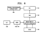
- FIG. 6 is a functional block diagram of the optical head of FIG. 3 ;
- FIG. 7A is a cross-sectional view of a leaky mode directional coupler (LMDC) and a hologram beam coupler (HBC) constituting the beam input/output coupler of the optical head shown in FIG. 3 ; and FIG. 7B shows a waveguide refractive index of the planar waveguide and the layers constituting the LMDC shown in FIG. 7A ;
- LMDC leaky mode directional coupler
- HBC hologram beam coupler
- FIG. 8 is a table of thickness and refractive index difference of the layers constituting the LMDC in FIGS. 7A-7B ;
- FIG. 9 is a graph illustrating the power transmitting characteristics of the LMDC shown in FIG. 7A-7B .
- FIG. 3 is an enlarged perspective view of an optical head for recording and/or reproducing information on an optical or magneto-optical disc according to an embodiment of the present invention.
- the optical head includes a beam input/output coupler 136 formed in an area of a planar waveguide (slab waveguide) 106 having a single mode.
- the beam input/output coupler 136 is shown enlarged for clarity of detail. It is noted that some individual parts such as the beam/output coupler 136 shown in FIG. 3 or other figures of the present disclosure may not be drawn to scale.
- the planar waveguide 106 includes a planar core layer 102 and a lower clad layer 104 that are formed on a portion of a substrate 100 , which may be a silica substrate.
- a clad layer 118 is formed on the lower clad layer 104 of the planar waveguide 106 .
- portions of the clad layer 118 are not shown to expose the planar waveguide 106 , particularly the lower clad layer 104 .
- the clad layer 118 , the lower clad layer 104 , the planar core layer 102 , and the substrate 100 are etched to form beam-shaping mirrors (BSMs) 132 and 134 near the corners of the substrate 100 as shown in FIG. 3 .
- a signal mirror (SM) 142 is formed at a sidewall of the substrate 100 .
- the clad layer 118 , the lower clad layer 104 , the planar core layer 102 , and the substrate 100 are etched so that the planar core layer 102 of the planar waveguide 106 is exposed by etching, and then a metal thin film having a high reflectance such as aluminum or gold is filled inside the etched portions.
- the beam input/output coupler 136 is positioned on a portion of the lower clad layer 104 of the planar wave guide layer 106 near the BSMs 132 , 134 .
- the beam input/output coupler 136 includes a leaky mode directional coupler (LMDC) 114 , a hologram beam coupler 116 , a PBS 120 , a quarter wave plate 122 , and an aberration correction (AC) layer 124 .
- An objective lens 138 and a disc 140 are positioned on or above the beam input/output coupler 136 .
- An LD 130 i.e., a light transmitting element
- PDs 144 i.e., light receiving elements
- the LD 130 transmits a beam in the planar core layer 102 of the planar waveguide 106
- the height of the light emitting portion in the LD 130 is preferably equal to the height of the planar core layer 102 .
- the LD 130 may be installed in any position for satisfactory transmission of the beam in the planar core layer 102 .
- a predetermined portion of the planar waveguide 106 may be etched to form the LD 130 in the etched portion, or the LD 130 may be separately installed outside the planar waveguide 106 .
- the PDs 144 receive beams guided by the planar core layer 102 of the planar waveguide 106 , and the height of the beam receiving portion in each PD 144 is preferably equal to the height of the planar core layer 102 . Similar to the LD 130 installation technique, the PDs 144 may be installed through an etched area of the planar waveguide 106 , or alternatively the PDs 144 may be separately installed outside the planar waveguide 106 .
- the beam emitted from the LD 130 propagates in the planar core layer 102 of the planar waveguide 106 .
- the path of the beam is then corrected by the BSMs 132 , 134 positioned as a reflective sidewall as shown in FIG. 3 .
- the beam emitted from the LD 130 and reflected by the BSMs 132 , 134 is then “leaked” into the beam input/output coupler 136 .
- the beam input/output coupler 136 redirects the propagating beam inside the planar core layer 102 to vertically come out of the planar waveguide 106 through the beam input/output coupler 136 and then to pass through the objective lens 138 .
- the beam that has passed through the objective lens 138 is incident on the disc 140 formed parallel to the planar waveguide 106 so as to record (i.e., write) and/or reproduce (i.e., read) information on or from the disc 140 .
- the beam reflected off the disc 140 enters the beam input/output coupler 136 and then propagates along the planar core layer 102 of the planar waveguide 106 but now corrected by the SM 142 (instead of the SMs 132 , 134 ) to be received by the PDs 144 .
- the beam input/output coupler 136 is formed as an optical thin film compising a plurality of layers that are installed on an area of the planar waveguide 106 .
- the thickness of the beam input/output coupler 136 is preferably equal to or less than the total combined thickness of the substrate 100 , the planar planar waveguide 106 , and the clad layer 118 .
- the thickness of the optical head can be innovatively reduced.
- the characteristics of the planar waveguide or the beam input/output coupler can be controlled so that a light transmitting element is compatible with a blue ray disc (BD) using a blue laser beam having a short wavelength as well as infrared rays or a red laser beam used for a CD or a DVD.
- BD blue ray disc
- an optical head compatible with various types of optical discs can be embodied, and a thickness of the optical head can be remarkably reduced. As a result, discs can be made to be compact.
- FIG. 4 is a plan view illustrating an exemplary path of the propagating beam in the planar waveguide 106 of the optical head
- FIG. 5 is a cross-sectional view illustrating the structure of the beam input/output coupler 136 of the optical head
- FIG. 6 is a functional block diagram of the optical head.
- the optical head shown in FIGS. 4-5 includes the planar waveguide 106 comprising the lower clad layer 104 , the planar core layer 102 , and the substrate 100 (all of which are shown in FIG. 3 ) and has a single mode.
- the LD 130 is a light transmitting element emitting (radiating or transmitting) a beam into the planar waveguide layer 106 .
- the PDs 144 are light detecting elements detecting the beams propagating in the planar waveguide layer 106 .
- the beam input/output coupler 136 directs the path of the beam leaked into the beam input/output coupler 136 from the planar waveguide layer 106 such that the beam exiting the input/output coupler 136 is substantially perpendicular the planar waveguide layer 106 . Similarly, the beam input/output coupler 136 allows the beam reflected off the disc 140 to propagate in the planar waveguide layer 106 .
- the beam entering and exiting the input/output coupler 136 is described to be substantially perpendicular to the planar waveguide layer 106 ; however, non-perpendicular angles of beam path entering and exiting the input/output coupler 136 with respect to the planar waveguide layer 106 is also possible and within the scope and spirit of the present disclosure.
- the structure and function of the beam input/output coupler 136 inputting and/or outputting the beam vertically from the ground is described in more detail below.
- the beam emitted by the LD 130 propagates in the planar core layer 102 of the planar waveguide 106 and its path is corrected by the BSMs 132 , 134 .
- the optical parts such as the BSMs 132 and 134 also provide beam extension function.
- the beam comes out of the planar waveguide 106 through the beam input/output coupler 136 in a direction perpendicular to the direction of the propagating beam in the planar waveguide 106 and then passes it to the objective lens 138 .
- the beam passing through the objective lens 138 is incident on the disc 140 (which is parallel to the planar waveguide 106 ) to write or read information on the disc 140 .
- the reflected beam offthe disc 140 enters the planar waveguide 106 through the beam input/output coupler 136 , as already explained above, for reception by the PDs 144 via the SM 142 .
- the beam received by the PDs 144 are then inputted to a signal processing circuit unit 146 (shown in FIG. 6 ).
- the beam input/output coupler 136 as shown in FIG. 4-6 is formed as an optical thin film comprising many layers, and details about the layers, which innovatively contributes to reducing the thickness of the optical head, are described in more detail below.
- the thickness of the beam input/output coupler 136 may be in the range of 100 ⁇ m to 200 ⁇ m.
- the layers of the optical thin film of the beam input/output coupler 136 according to an embodiment of the present invention include the LMDC 114 , the hologram beam coupler 116 positioned on the LMDC 114 , the PBS 120 positioned on the hologram beam coupler 116 , the quarter wave plate 122 , and the AC layer 124 .
- the LMDC 114 emits a beam proceeding toward the planar waveguide 106 upward at a predetermined angle with the planar waveguide 106 or allows a beam reflected from the disc 140 to be incident on the planar waveguide 106 .
- the hologram beam coupler 116 emits the beam having passed through the LMDC 114 vertically from the ground or allows the beam reflected from the disc 140 to be incident on the LMDC 114 at a predetermined angle with the LMDC 114 .
- the PBS 120 and the quarter wave plate 122 polarize and pass the beam having passed through the LMDC 114 and the hologram beam coupler 116 and refract the polarized beam that is reflected from the disc 140 and incident on the beam input/output coupler 136 to change a traveling direction of the beam.
- the traveling direction of the beam is changed, the beam is incident on the PDs 144 through the SM 142 .
- the AC layer 124 corrects the aberration of the beam input/output coupler 136 formed of multi-layer thin films.
- FIG. 7A is a cross-sectional view of the LMDC 114 and the hologram beam coupler 116 of the beam input/output coupler 136 on the planar waveguide layer 106 of the optical head of an embodiment of the present invention.
- FIG. 7B shows the waveguide refractive index of the LMDC 114 .
- FIG. 8 is a table of thicknesses and refractive index differences of layers of the LMDC 114 .
- the LMDC 114 includes a leaky core layer 108 , an inner clad layer 110 , and the upper clad layer 112 .
- the present invention as described and shown uses a waveguide mode in which a beam propagates along inside the planar core layer 102 of the planar waveguide 106 and a leaky mode in which a beam propagates through the leaky core layer 108 of the LMDC 114 , thereby “leaking” the beam from the planar waveguide layer 106 toward the hologram beam coupler 116 through the LMDC 114 , and in the reverse order.
- FIG. 1 the waveguide mode in which a beam propagates along inside the planar core layer 102 of the planar waveguide 106
- a leaky mode in which a beam propagates through the leaky core layer 108 of the LMDC 114
- the left part of the cross-sectional view denotes the characteristics of the beam only when the waveguide mode is in operation
- the right part of the cross-section i.e., toward 126 d
- the reference numerals 126 a through 126 d denote the distribution of the beam strength in each layer of the cross-section from the waveguide mode (as in 126 a ) to the couple wave guide mode and leaky mode (as in 126 d ).
- the leaky core layer 108 of the LMDC 114 is formed on the planar waveguide 106 .
- the planar waveguide 106 includes the substrate 100 , the planar core layer 102 that is formed on the substrate 100 and has a refractive index n 2 , and a portion of the lower clad layer 104 having a refractive index n, lower than the refractive index n 2 .
- the thicknesses of the planar core layer 102 and the lower clad layer 104 are preferably 2.0 ⁇ m and 1.2 ⁇ m, respectively.
- FIG. 7B shows refractive indexes of the layers constituting the planar waveguide 106 and the layers constituting the LMDC 114 .
- n 1 denotes the refractive index of the lower clad layer 104
- n 2 denotes the refractive index of the planar core layer 102
- n 3 denotes the refractive index of the leaky core layer 108
- n 4 denotes the refractive index of an inner clad layer 110
- n 5 denotes the refractive index of the upper clad layer 112 .
- the LMDC 114 contacting a portion of the lower clad layer 104 includes:
- ⁇ n denotes the difference between the refractive index of a layer and the refractive index of the substrate 100 having the lowest refractive index.
- ⁇ n of the planar core layer 102 i.e., the refractive index difference between the planar core layer 102 and the substrate 100
- ⁇ n of the leaky core layer 108 i.e., the refractive index difference between the leaky core layer 108 and the substrate 100
- ⁇ n of the lower clad layer is zero meaning that the refractive index of the lower clad layer 104 equals the refractive index of the substrate 100 .
- the refractive index of a particular optical material is affected also by the wavelength of the light; therefore, the same material subjected to different light wavelengths may exhibit slightly different refractive indexes
- the above-mentioned refractive indexes are one set of exemplary values of the shown layers subjected to a blue light having a wavelength of 405 nm.
- the refractive index of the substrate 100 is 1.4702. Nevertheless, it should be noted that the scope of the present invention is not limited to those refractive indexes as shown in FIG. 8 . Other wavelengths of light besides the blue light can be used to produce the same intended results as described and claimed herein without deviating the scope and spirit of the present invention.
- a beam emitted by the LD 130 and being propagated in the planar waveguide 106 will leak to the upper clad layer 112 due to the leaky mode formed by the different refractive indexes and the gap existing between the core layers, i.e., between the planar core layer 102 and the leaky core layer 108 , as shown in FIGS. 7 and 8 . If the beams proceeding toward the planar core layer 102 are incident on the LMDC 114 and a condition n 5 >n 4 >n 3 >n 2 >n 1 is satisfied, the leaky mode is formed. Under this leaky mode condition, the beams propagating in the planar core layer 102 of the planar waveguide 106 will leak to the LMCD 114 .
- the beams propagating in the planar core layer 102 will pass through the lower clad layer 104 and will be incident on the LMDC 114 , because the refractive index of the lower clad layer 104 is lower than the refractive index of the core layer 102 .
- the beams are able to propagate through the leaky core layer 108 . Since the refractive index of the inner clad layer 110 is low, the beams coupled and proceeding toward the leaky core layer 108 are leaked toward the upper clad layer 112 at a predetermined angle.
- the LMDC 114 controls the refractive index of the upper clad layer 112 to control an amount and an angle of the beam propagated to the upper clad layer 112 and controls the thickness of the inner clad layer 110 to control coupling efficiency and a coupling length.
- the LMDC 114 has a leaky beam having a maximum leaky effect and a Gaussian distribution within a range of (b ⁇ L/ 2 ) ⁇ Y ⁇ (b+L/ 2 ), where b denotes a distance from a beam input to the LMDC 114 to the center of the LMDC 114 , L denotes a diameter of the LMDC 114 , and Y denotes both ends of the LMDC 114 .
- the beam incident on the planar core layer 102 of the planar waveguide 106 by the LD 130 proceeds from the left toward the right and then is incident on a starting point b ⁇ L/ 2 of the LMDC 114 .
- the thickness of the lower clad layer 104 is controlled to sufficiently transmit a power from the waveguide mode toward the leaky mode so that a power of the waveguide mode is vanished at an ending side “b+L/ 2 ” of the planar waveguide 106 .
- the power transmitted from the waveguide mode toward the leaky mode generates a leaky beam, maintaining a predetermined angle.
- the leaky beam is refracted by the hologram beam coupler 116 to proceed in a vertical direction so as to be transmitted toward the disc 140 .
- FIG. 9 is a graph illustrating the power-transmitting characteristics of the LMDC 114 .
- the distribution of an input beam propagated toward a hologram beam coupler may be formed in the form of Gaussian function.
- Beam loss of a leaky mode is reduced in index number along a direction toward which a beam proceeds as marked with reference numeral 203 .
- Beam coupling toward the leaky mode is accumulated and increased along the direction toward which the beam proceeds as marked with reference numeral 201 .
- a power distribution of a leaky beam that is a product of the beam loss and the beam coupling may be formed in the form of the Gaussian function as marked with reference numeral 205 .
- Reference numeral 203 denotes a power of the leaky mode reduced along the direction toward which the beam proceeds
- reference numeral 201 denotes the power of the leaky mode accumulated along the direction
- reference numeral 205 denotes a power distribution of the leaky beam propagated to a hologram beam coupler.
- the optical parts necessary for forming the beams can be made of thin films on the planar waveguide.
- the thicknesses of the optical parts are limited to a thickness of a waveguide.
- a thickness of the optical head can be innovatively reduced.
- individual optical parts necessary for the optical head are integrated on the planar waveguide having a single mode so as to be formed as individual bodies.
- the thickness of the optical head can be reduced.
- the characteristics of the planar waveguide or the beam input/output coupler can be controlled so that a light transmitting element is compatible with a BD using a blue laser beam having a short wavelength as well as infrared rays or a red laser beam used for a CD or a DVD.
- the optical head can be compatible with various types of discs. Also, the thickness of the optical head can be remarkably reduced. As a result, discs can be made compact.
Landscapes
- Physics & Mathematics (AREA)
- Optics & Photonics (AREA)
- Optical Head (AREA)
- Optical Integrated Circuits (AREA)
- Optical Couplings Of Light Guides (AREA)
Abstract
Description
- This application claims the benefit of Korean Patent Application Nos. 10-2004-0103073 filed on Dec. 8, 2004 and 10-2005-0053053 filed on Jun. 20, 2005 in the Korean Intellectual Property Office, the disclosures of which are incorporated herein in their entirety by reference.
- 1. Field of the Invention
- The present invention relates generally to an optical head recording and/or reproducing information on or from an optical or magneto-optical disc (disk) using optical or magneto-optical characteristics, and more particularly, to an optical head having an innovatively reduced thickness.
- 2. Description of the Related Art
- In general, optical heads are used to record and/or reproduce information on or from compact discs (CDs), digital versatile discs (DVDs), blue-ray discs (BDs), or MP3 players using optical discs. An optical head includes many individual optical parts such as the light transmitting/receiving elements (i.e., the light emitting/receiving elements including a laser diode (LD) and a photo diode (PD)), a mirror, a prism, a beam splitter (BS), a polarization beam splitter (PBS), and a hologram optical element (HOE).
- An optical head is made by assembling these individual optical parts each of which has thickness and volume in the 3-dimensional space, and this is an obstacle to reducing the overall thickness of the optical head. However, reduction of the optical head thickness is an important design requirement of the modern mobile optical discs, which are no longer stationary but are portable devices, i.e., easily carryable and movable. To achieve this, the thickness of the optical head must be innovatively reduced.
-
FIG. 1 is a cross-sectional view of an example of an optical head used in an MP3 player according to prior art. - The optical head shown in
FIG. 1 is published in PCT International Application No. PCT/US02/00875 and PCT International Publication No. WO 02/058059 A2, entitled “Beamshaper for Optical Head” by Dataplay, INC. In the optical head shown inFIG. 1 , anLD 4, aPD 6, anobjective lens 8, aprism 10, amirror 12, and aPBS 14 are disposed 3-dimensionally on asubstrate 2. As shown inFIG. 1 , thebeam 20 emitted from theLD 4 is incident on adisc 16 through theprism 10, themirror 12, thePBS 14, and theobjective lens 8. Thebeam 20 is reflected from thedisc 16 and then incident on thePD 6 through the PBS 14. - Because each of the optical parts in the optical head as shown in
FIG. 1 has a predetermined volume and disposed in the 3-dimensional space, the overall thickness of the optical head, even if theobjective lens 8 is excluded, ends up being undesirably large for mobility. This also means that the overall thickness of an optical head such as that shown inFIG. 1 may not be readily reduced as long as many individual parts as shown inFIG. 1 are assembled into an optical head, mainly because the thickness of each of the individual parts will add up. -
FIG. 2 is a cross-sectional view of another prior art example of an optical head for a BD using a blue laser beam manufactured by Sony Corporation. - The optical head shown in
FIG. 2 is published in February 2003, entitled “Small Integrated Optical Head Device Using a Blue-violet Laser Diode for Blue-ray Disc System,” Jpn. J. Appl. Phys. Vol. 42(2003), pp. 880-884,Part 1. No. 2B. - The optical head shown in
FIG. 2 includes optical parts such as ablue beam LD 30, a 45degree mirror 32, a half wave plate (HWP) 34, agrating 36, aPBS 38, amirror 40, aHOE 42, acylinder lens 44, aprism 46, a molded optical element, aPD IC 50, and apackage 54 molded by alead frame 52. - As shown in
FIG. 2 , thebeam 56 emitted from theblue beam LD 30 is incident on a disc through the 45degree mirror 32, the HWP 34, thegrating 36, and thePBS 38. Thebeam 56 is reflected from the disc and then incident on thePD IC 50 through thePBS 38, themirror 40, theHOE 42, and thecylinder lens 44. - The optical parts in the optical head shown in
FIG. 2 are also disposed in a 3-dimensional space. In the optical head shown inFIG. 2 , theHOE 42 is used; however, the overall thickness of the optical head still cannot be sufficiently and greatly reduced because the individual parts each occupying a predetermined volume in the 3-dimensional space are still used to assemble the optical head shown inFIG. 2 . - As described above, the optical parts in a conventional optical head are disposed in a 3-dimensional space. This limits effective reduction of the overall thickness of a conventional optical head. As a result, the undesirable thickness of the conventional optical heads presents a fundamental obstacle to putting them together in an easily carryable, mobile optical disc for its intended practical portable use.
- The present invention provides an optical head including optical parts that are not disposed on a 3-dimensional space.
- The present invention also provides an optical head considerably reducing a thickness thereof by positioning optical parts on a planar waveguide having a single mode.
- According to an aspect of the present invention, there is provided an optical head including: a light transmitting element emitting a beam; a planar waveguide formed on a substrate and receiving the beam oscillated from the light transmitting element; a beam input/output coupler integrated as a thin film on a portion of the planar waveguide and receiving the beam through the planar waveguide to transmit the beam vertically toward a disc positioned above the planar waveguide or transmitting the beam reflected from the disc through the planar waveguide; and light receiving elements receiving the beam propagated to the planar waveguide through the beam input/output coupler.
- According to another aspect of the present invention, there is provided an optical head including: a light transmitting element emitting a beam; a planar waveguide formed on a substrate and receiving the beam oscillated from the light transmitting element; beam shaping mirrors positioned on a side of the substrate and changing a path of the beam oscillated from the light transmitting element and transmitted to the planar waveguide; a beam input/output coupler integrated as a thin film on a portion of the planar waveguide, receiving the beam having the changed path to transmit the beam vertically toward a disc positioned above the planar waveguide so as to record information and/or reproduce (read) information from the disc, and transmitting the beam reflected from the disc through the planar waveguide; a signal mirror positioned on a side of the substrate and changing a path of the beam transmitted to the planar waveguide through the beam input/output coupler; light receiving elements receiving the beam having the changed path through the planar waveguide; and a signal processing circuit unit signal-processing the beam transmitted from the light receiving elements.
- The above and other features and advantages of the present invention will become more apparent by describing in detail exemplary embodiments thereof with reference to the attached drawings in which:
-
FIG. 1 is a cross-sectional view of an optical head according to prior art; -
FIG. 2 is a cross-sectional view of another optical head according to prior art; -
FIG. 3 is an enlarged perspective view of an optical head for recording and/or reproducing information on or from an optical or magneto-optical disc according to an embodiment of the present invention; -
FIGS. 4 and 5 are a plan view and a cross-sectional view, respectively, of the optical head shown inFIG. 3 ; -
FIG. 6 is a functional block diagram of the optical head ofFIG. 3 ; -
FIG. 7A is a cross-sectional view of a leaky mode directional coupler (LMDC) and a hologram beam coupler (HBC) constituting the beam input/output coupler of the optical head shown inFIG. 3 ; andFIG. 7B shows a waveguide refractive index of the planar waveguide and the layers constituting the LMDC shown inFIG. 7A ; -
FIG. 8 is a table of thickness and refractive index difference of the layers constituting the LMDC inFIGS. 7A-7B ; and -
FIG. 9 is a graph illustrating the power transmitting characteristics of the LMDC shown inFIG. 7A-7B . - The present invention will now be described more fully with reference to the accompanying drawings, in which exemplary embodiments of the invention are shown. The invention may, however, be embodied in many different forms and should not be construed as being limited to the embodiments set forth herein; rather, these embodiments are provided so that this disclosure will be thorough and complete, and will fully convey the concept of the invention to those skilled in the art. In the drawings, thickness of the layers and regions are exaggerated for clarity.
-
FIG. 3 is an enlarged perspective view of an optical head for recording and/or reproducing information on an optical or magneto-optical disc according to an embodiment of the present invention. - As shown in
FIG. 3 , the optical head according to an embodiment of the present invention includes a beam input/output coupler 136 formed in an area of a planar waveguide (slab waveguide) 106 having a single mode. InFIG. 3 , the beam input/output coupler 136 is shown enlarged for clarity of detail. It is noted that some individual parts such as the beam/output coupler 136 shown inFIG. 3 or other figures of the present disclosure may not be drawn to scale. Theplanar waveguide 106 includes aplanar core layer 102 and alower clad layer 104 that are formed on a portion of asubstrate 100, which may be a silica substrate. Aclad layer 118 is formed on thelower clad layer 104 of theplanar waveguide 106. InFIG. 3 , portions of theclad layer 118 are not shown to expose theplanar waveguide 106, particularly the lowerclad layer 104. - The
clad layer 118, the lowerclad layer 104, theplanar core layer 102, and thesubstrate 100 are etched to form beam-shaping mirrors (BSMs) 132 and 134 near the corners of thesubstrate 100 as shown inFIG. 3 . A signal mirror (SM) 142 is formed at a sidewall of thesubstrate 100. To fabricate theBSMs SM 142 shown inFIG. 3 , theclad layer 118, the lowerclad layer 104, theplanar core layer 102, and thesubstrate 100 are etched so that theplanar core layer 102 of theplanar waveguide 106 is exposed by etching, and then a metal thin film having a high reflectance such as aluminum or gold is filled inside the etched portions. - The beam input/
output coupler 136 is positioned on a portion of the lowerclad layer 104 of the planarwave guide layer 106 near theBSMs output coupler 136 includes a leaky mode directional coupler (LMDC) 114, ahologram beam coupler 116, aPBS 120, aquarter wave plate 122, and an aberration correction (AC)layer 124. Anobjective lens 138 and adisc 140 are positioned on or above the beam input/output coupler 136. - An LD 130 (i.e., a light transmitting element) and PDs 144 (i.e., light receiving elements) are positioned above a portion of the
substrate 100. TheLD 130 transmits a beam in theplanar core layer 102 of theplanar waveguide 106, and the height of the light emitting portion in theLD 130 is preferably equal to the height of theplanar core layer 102. TheLD 130 may be installed in any position for satisfactory transmission of the beam in theplanar core layer 102. In other words, a predetermined portion of theplanar waveguide 106 may be etched to form theLD 130 in the etched portion, or theLD 130 may be separately installed outside theplanar waveguide 106. - The
PDs 144 receive beams guided by theplanar core layer 102 of theplanar waveguide 106, and the height of the beam receiving portion in eachPD 144 is preferably equal to the height of theplanar core layer 102. Similar to theLD 130 installation technique, thePDs 144 may be installed through an etched area of theplanar waveguide 106, or alternatively thePDs 144 may be separately installed outside theplanar waveguide 106. - In operation, the beam emitted from the LD 130 (i.e., the light transmitting element) propagates in the
planar core layer 102 of theplanar waveguide 106. The path of the beam is then corrected by theBSMs FIG. 3 . The beam emitted from theLD 130 and reflected by theBSMs output coupler 136. The beam input/output coupler 136 redirects the propagating beam inside theplanar core layer 102 to vertically come out of theplanar waveguide 106 through the beam input/output coupler 136 and then to pass through theobjective lens 138. The beam that has passed through theobjective lens 138 is incident on thedisc 140 formed parallel to theplanar waveguide 106 so as to record (i.e., write) and/or reproduce (i.e., read) information on or from thedisc 140. - The beam reflected off the
disc 140 enters the beam input/output coupler 136 and then propagates along theplanar core layer 102 of theplanar waveguide 106 but now corrected by the SM 142 (instead of theSMs 132, 134) to be received by thePDs 144. - The beam input/
output coupler 136 is formed as an optical thin film compising a plurality of layers that are installed on an area of theplanar waveguide 106. The thickness of the beam input/output coupler 136 is preferably equal to or less than the total combined thickness of thesubstrate 100, the planarplanar waveguide 106, and theclad layer 118. Thus, in the present invention, the thickness of the optical head can be innovatively reduced. - In addition, according to an embodiment of the present invention, the characteristics of the planar waveguide or the beam input/output coupler can be controlled so that a light transmitting element is compatible with a blue ray disc (BD) using a blue laser beam having a short wavelength as well as infrared rays or a red laser beam used for a CD or a DVD. Thus, an optical head compatible with various types of optical discs can be embodied, and a thickness of the optical head can be remarkably reduced. As a result, discs can be made to be compact.
- With reference to
FIGS. 4-6 , the structure of the optical head is described in detail.FIG. 4 is a plan view illustrating an exemplary path of the propagating beam in theplanar waveguide 106 of the optical head, andFIG. 5 is a cross-sectional view illustrating the structure of the beam input/output coupler 136 of the optical head.FIG. 6 is a functional block diagram of the optical head. - The optical head shown in
FIGS. 4-5 according to an embodiment of the present invention includes theplanar waveguide 106 comprising the lowerclad layer 104, theplanar core layer 102, and the substrate 100 (all of which are shown inFIG. 3 ) and has a single mode. TheLD 130 is a light transmitting element emitting (radiating or transmitting) a beam into theplanar waveguide layer 106. ThePDs 144 are light detecting elements detecting the beams propagating in theplanar waveguide layer 106. The beam input/output coupler 136 directs the path of the beam leaked into the beam input/output coupler 136 from theplanar waveguide layer 106 such that the beam exiting the input/output coupler 136 is substantially perpendicular theplanar waveguide layer 106. Similarly, the beam input/output coupler 136 allows the beam reflected off thedisc 140 to propagate in theplanar waveguide layer 106. In this embodiment, the beam entering and exiting the input/output coupler 136 is described to be substantially perpendicular to theplanar waveguide layer 106; however, non-perpendicular angles of beam path entering and exiting the input/output coupler 136 with respect to theplanar waveguide layer 106 is also possible and within the scope and spirit of the present disclosure. The structure and function of the beam input/output coupler 136 inputting and/or outputting the beam vertically from the ground is described in more detail below. - As shown in
FIGS. 4-6 , the beam emitted by theLD 130 propagates in theplanar core layer 102 of theplanar waveguide 106 and its path is corrected by theBSMs BSMs - The beam comes out of the
planar waveguide 106 through the beam input/output coupler 136 in a direction perpendicular to the direction of the propagating beam in theplanar waveguide 106 and then passes it to theobjective lens 138. The beam passing through theobjective lens 138 is incident on the disc 140 (which is parallel to the planar waveguide 106) to write or read information on thedisc 140. The reflected beam offthedisc 140 enters theplanar waveguide 106 through the beam input/output coupler 136, as already explained above, for reception by thePDs 144 via theSM 142. The beam received by thePDs 144 are then inputted to a signal processing circuit unit 146 (shown inFIG. 6 ). - The beam input/
output coupler 136 as shown inFIG. 4-6 is formed as an optical thin film comprising many layers, and details about the layers, which innovatively contributes to reducing the thickness of the optical head, are described in more detail below. The thickness of the beam input/output coupler 136 may be in the range of 100 μm to 200 μm. The layers of the optical thin film of the beam input/output coupler 136 according to an embodiment of the present invention include theLMDC 114, thehologram beam coupler 116 positioned on theLMDC 114, thePBS 120 positioned on thehologram beam coupler 116, thequarter wave plate 122, and theAC layer 124. - The
LMDC 114 emits a beam proceeding toward theplanar waveguide 106 upward at a predetermined angle with theplanar waveguide 106 or allows a beam reflected from thedisc 140 to be incident on theplanar waveguide 106. Thehologram beam coupler 116 emits the beam having passed through theLMDC 114 vertically from the ground or allows the beam reflected from thedisc 140 to be incident on theLMDC 114 at a predetermined angle with theLMDC 114. - The
PBS 120 and thequarter wave plate 122 polarize and pass the beam having passed through theLMDC 114 and thehologram beam coupler 116 and refract the polarized beam that is reflected from thedisc 140 and incident on the beam input/output coupler 136 to change a traveling direction of the beam. When the traveling direction of the beam is changed, the beam is incident on the PDs 144 through theSM 142. TheAC layer 124 corrects the aberration of the beam input/output coupler 136 formed of multi-layer thin films. -
FIG. 7A is a cross-sectional view of theLMDC 114 and thehologram beam coupler 116 of the beam input/output coupler 136 on theplanar waveguide layer 106 of the optical head of an embodiment of the present invention.FIG. 7B shows the waveguide refractive index of theLMDC 114.FIG. 8 is a table of thicknesses and refractive index differences of layers of theLMDC 114. - As shown in
FIG. 7 , theLMDC 114 includes aleaky core layer 108, an inner cladlayer 110, and the upper cladlayer 112. The present invention as described and shown uses a waveguide mode in which a beam propagates along inside theplanar core layer 102 of theplanar waveguide 106 and a leaky mode in which a beam propagates through theleaky core layer 108 of theLMDC 114, thereby “leaking” the beam from theplanar waveguide layer 106 toward thehologram beam coupler 116 through theLMDC 114, and in the reverse order. InFIG. 7 , the left part of the cross-sectional view (i.e., toward 126 a) denotes the characteristics of the beam only when the waveguide mode is in operation, and the right part of the cross-section (i.e., toward 126 d) indicates that the characteristics of the beam when the waveguide mode is coupled to the leaky mode. Thereference numerals 126 a through 126 d denote the distribution of the beam strength in each layer of the cross-section from the waveguide mode (as in 126 a) to the couple wave guide mode and leaky mode (as in 126 d). - The
leaky core layer 108 of theLMDC 114 is formed on theplanar waveguide 106. Theplanar waveguide 106 includes thesubstrate 100, theplanar core layer 102 that is formed on thesubstrate 100 and has a refractive index n2, and a portion of the lowerclad layer 104 having a refractive index n, lower than the refractive index n2. The thicknesses of theplanar core layer 102 and the lowerclad layer 104 are preferably 2.0 μm and 1.2 μm, respectively. -
FIG. 7B shows refractive indexes of the layers constituting theplanar waveguide 106 and the layers constituting theLMDC 114. n1 denotes the refractive index of the lowerclad layer 104, n2 denotes the refractive index of theplanar core layer 102, n3 denotes the refractive index of theleaky core layer 108, n4 denotes the refractive index of an inner cladlayer 110, and n5 denotes the refractive index of the upper cladlayer 112. - Thus, the
LMDC 114 contacting a portion of the lowerclad layer 104 includes: -
- (1) the
leaky core layer 108 having the refractive index n3 greater than the refractive index n2; - (2) the inner clad
layer 110 having the refractive index n4 greater than the refractive index n3; and - (3) the upper clad
layer 112 having the refractive index n5 greater than the refractive index n4.
Thus, n5 (of the layer 112)>n4 (of the layer 110)>n3 (of the layer 108)>n2 (of the layer 102). The thickness of theleaky core layer 108, the inner cladlayer 110, and the upper cladlayer 112 are preferably 1.8 μm, 0.2 μm, and 1 μm, respectively.
- (1) the
- In the “thickness” column of
FIG. 8 , the numerical value in parenthesis next to each thickness of the respective layer denotes the the thickness of the respective layer of theLMDC 114 but with reference to the surface of the inner cladlayer 110 being 0, that is, X=0 at the surface of the inner cladlayer 110. In this regard, -
- (1) the value X of the upper clad
layer 112 is less than “0,” which means for example that 1 μm thick upper clad layer is located in the direction above the surface of the inner cladlayer 110; - (2) the value X of the inner clad
layer 110 is more than or equal to “0” but less than 0.2, which means for example that 0.2 μm thick innerclad layer 110 is located 0 to 0.2 μm in the direction below (or opposite the direction referenced in the X of the upper clad layer 112) the surface of the inner cladlayer 110; - (3) the value X of the
leaky core layer 108 is more than or equal to 0.2 bt less than 3.0, which means for example that 1.8 μm thickleaky core layer 108 is located 0.2 to 3.0 μm below the surface of the inner cladlayer 110; and - (4) the value X of the
substrate 100 is more than or equal to 6.0, which means for example that a ratherthick substrate layer 100 is located beginning 6.0 μm for example below the surface of theclad layer 110.
- (1) the value X of the upper clad
- In the last column of
FIG. 8 , □n denotes the difference between the refractive index of a layer and the refractive index of thesubstrate 100 having the lowest refractive index. Thus, □n of the planar core layer 102 (i.e., the refractive index difference between theplanar core layer 102 and the substrate 100) is 0.0027, □n of the leaky core layer 108 (i.e., the refractive index difference between theleaky core layer 108 and the substrate 100) is 0.0036, and □n of the lower clad layer is zero meaning that the refractive index of the lowerclad layer 104 equals the refractive index of thesubstrate 100. - In general, the refractive index of a particular optical material is affected also by the wavelength of the light; therefore, the same material subjected to different light wavelengths may exhibit slightly different refractive indexes The above-mentioned refractive indexes are one set of exemplary values of the shown layers subjected to a blue light having a wavelength of 405 nm. In this case, the refractive index of the
substrate 100 is 1.4702. Nevertheless, it should be noted that the scope of the present invention is not limited to those refractive indexes as shown inFIG. 8 . Other wavelengths of light besides the blue light can be used to produce the same intended results as described and claimed herein without deviating the scope and spirit of the present invention. - The operations and functions of the
LMDC 114 and thehologram beam coupler 116 will now be described. - In detail, a beam emitted by the
LD 130 and being propagated in theplanar waveguide 106 will leak to the upper cladlayer 112 due to the leaky mode formed by the different refractive indexes and the gap existing between the core layers, i.e., between theplanar core layer 102 and theleaky core layer 108, as shown inFIGS. 7 and 8 . If the beams proceeding toward theplanar core layer 102 are incident on theLMDC 114 and a condition n5>n4>n3>n2>n1 is satisfied, the leaky mode is formed. Under this leaky mode condition, the beams propagating in theplanar core layer 102 of theplanar waveguide 106 will leak to theLMCD 114. - In other words, the beams propagating in the
planar core layer 102 will pass through the lowerclad layer 104 and will be incident on theLMDC 114, because the refractive index of the lowerclad layer 104 is lower than the refractive index of thecore layer 102. Thus, the beams are able to propagate through theleaky core layer 108. Since the refractive index of the inner cladlayer 110 is low, the beams coupled and proceeding toward theleaky core layer 108 are leaked toward the upper cladlayer 112 at a predetermined angle. An angle θ of the beam propagated to the upper cladlayer 112 is determined as in Equation 1:
θ=sin−1(β2/(n5/k0)) (1)
wherein β2 denotes a propagation constant in theLMDC 114, k0 denotes a propagation constant in a vacuum state, and n5 denotes the refractive index of the upper cladlayer 112. TheLMDC 114 controls the refractive index of the upper cladlayer 112 to control an amount and an angle of the beam propagated to the upper cladlayer 112 and controls the thickness of the inner cladlayer 110 to control coupling efficiency and a coupling length. - The
LMDC 114 has a leaky beam having a maximum leaky effect and a Gaussian distribution within a range of (b−L/2)<Y<(b+L/2), where b denotes a distance from a beam input to theLMDC 114 to the center of theLMDC 114, L denotes a diameter of theLMDC 114, and Y denotes both ends of theLMDC 114. - In more detail, the beam incident on the
planar core layer 102 of theplanar waveguide 106 by theLD 130 proceeds from the left toward the right and then is incident on a starting point b−L/2 of theLMDC 114. Thus, the thickness of the lowerclad layer 104 is controlled to sufficiently transmit a power from the waveguide mode toward the leaky mode so that a power of the waveguide mode is vanished at an ending side “b+L/2” of theplanar waveguide 106. The power transmitted from the waveguide mode toward the leaky mode generates a leaky beam, maintaining a predetermined angle. The leaky beam is refracted by thehologram beam coupler 116 to proceed in a vertical direction so as to be transmitted toward thedisc 140. -
FIG. 9 is a graph illustrating the power-transmitting characteristics of theLMDC 114. - In detail, the distribution of an input beam propagated toward a hologram beam coupler may be formed in the form of Gaussian function. Beam loss of a leaky mode is reduced in index number along a direction toward which a beam proceeds as marked with
reference numeral 203. Beam coupling toward the leaky mode is accumulated and increased along the direction toward which the beam proceeds as marked withreference numeral 201. Thus, a power distribution of a leaky beam that is a product of the beam loss and the beam coupling may be formed in the form of the Gaussian function as marked withreference numeral 205. - If the leaky beam has the Gaussian function form, an optical distortion caused by an asymmetric distribution of a beam can be reduced, and a signal reflected from a disc can be coupled in a waveguide mode.
Reference numeral 203 denotes a power of the leaky mode reduced along the direction toward which the beam proceeds,reference numeral 201 denotes the power of the leaky mode accumulated along the direction, andreference numeral 205 denotes a power distribution of the leaky beam propagated to a hologram beam coupler. - As descried above, in an optical head having a beam input/output coupler on a planar waveguide according to an embodiment of the present invention, the optical parts necessary for forming the beams can be made of thin films on the planar waveguide. Also, the thicknesses of the optical parts are limited to a thickness of a waveguide. Thus, a thickness of the optical head can be innovatively reduced. In other words, individual optical parts necessary for the optical head are integrated on the planar waveguide having a single mode so as to be formed as individual bodies. Thus, the thickness of the optical head can be reduced.
- Also, the characteristics of the planar waveguide or the beam input/output coupler can be controlled so that a light transmitting element is compatible with a BD using a blue laser beam having a short wavelength as well as infrared rays or a red laser beam used for a CD or a DVD. Thus, the optical head can be compatible with various types of discs. Also, the thickness of the optical head can be remarkably reduced. As a result, discs can be made compact.
- While the present invention has been particularly shown and described with reference to exemplary embodiments thereof, it will be understood by those of ordinary skill in the art that various changes in form and details may be made therein without departing from the spirit and scope of the present invention as defined by the following claims.
Claims (19)
Applications Claiming Priority (4)
| Application Number | Priority Date | Filing Date | Title |
|---|---|---|---|
| KR10-2004-0103073 | 2004-12-08 | ||
| KR20040103073 | 2004-12-08 | ||
| KR10-2005-0053053 | 2005-06-20 | ||
| KR1020050053053A KR100701122B1 (en) | 2004-12-08 | 2005-06-20 | Optical head with beam exit coupler on planar waveguide |
Publications (2)
| Publication Number | Publication Date |
|---|---|
| US20060120249A1 true US20060120249A1 (en) | 2006-06-08 |
| US7580336B2 US7580336B2 (en) | 2009-08-25 |
Family
ID=36051488
Family Applications (1)
| Application Number | Title | Priority Date | Filing Date |
|---|---|---|---|
| US11/270,998 Expired - Fee Related US7580336B2 (en) | 2004-12-08 | 2005-11-10 | Optical head having a beam input/output coupler on a planar waveguide |
Country Status (3)
| Country | Link |
|---|---|
| US (1) | US7580336B2 (en) |
| EP (1) | EP1669987B1 (en) |
| JP (1) | JP4096004B2 (en) |
Cited By (2)
| Publication number | Priority date | Publication date | Assignee | Title |
|---|---|---|---|---|
| US20100044723A1 (en) * | 2008-08-25 | 2010-02-25 | Shinko Electric Industries Co., Ltd. | Package for photoelectric wiring and lead frame |
| TWI480605B (en) * | 2009-12-03 | 2015-04-11 | 三星電子股份有限公司 | Optical waveguide and coupler device and method and method of manufacturing same |
Families Citing this family (2)
| Publication number | Priority date | Publication date | Assignee | Title |
|---|---|---|---|---|
| JP2008089778A (en) * | 2006-09-29 | 2008-04-17 | Sumitomo Osaka Cement Co Ltd | Optical device and optical device manufacturing method |
| US11448815B2 (en) * | 2020-11-06 | 2022-09-20 | Meta Platforms Technologies LLC | Slab waveguide and projector with intermodal coupling |
Citations (9)
| Publication number | Priority date | Publication date | Assignee | Title |
|---|---|---|---|---|
| US4737946A (en) * | 1984-09-03 | 1988-04-12 | Omron Tateisi Electronics Co. | Device for processing optical data with improved optical allignment means |
| US4797867A (en) * | 1985-10-16 | 1989-01-10 | Fuji Photo Film Co., Ltd. | Pick-up head for optical information storage disk |
| US4861128A (en) * | 1987-02-04 | 1989-08-29 | Hitachi, Ltd. | Optical pickup using a waveguide |
| US4866694A (en) * | 1985-12-17 | 1989-09-12 | International Business Machines Corporation | Read/write head for optical disks |
| US5166989A (en) * | 1990-11-16 | 1992-11-24 | International Business Machines Corporation | Integrated polarization detection system |
| US5208800A (en) * | 1990-04-13 | 1993-05-04 | Ricoh Company, Ltd. | Mode splitter and magneto-optical signal detection device |
| US5701289A (en) * | 1995-06-23 | 1997-12-23 | Nec Corporation | Optical head with hologram couplers for reading and writing data |
| US20040042377A1 (en) * | 2002-09-02 | 2004-03-04 | Samsung Electronics Co., Ltd. | Integrated type optical head with coupler |
| US6999660B2 (en) * | 2003-07-08 | 2006-02-14 | Electronics And Telecommunications Research Institute | Highly efficient focusing waveguide grating coupler using leaky mode |
Family Cites Families (6)
| Publication number | Priority date | Publication date | Assignee | Title |
|---|---|---|---|---|
| JPS61248245A (en) | 1985-04-25 | 1986-11-05 | Mitsubishi Electric Corp | Optical head device |
| JPS63164033A (en) | 1986-12-26 | 1988-07-07 | Matsushita Electric Ind Co Ltd | Optical pickup device |
| US5070488A (en) | 1988-06-29 | 1991-12-03 | Atsuko Fukushima | Optical integrated circuit and optical apparatus |
| EP0360209A3 (en) | 1988-09-19 | 1992-08-19 | Hitachi, Ltd. | Optical head and optical data processing apparatus |
| WO1999031658A1 (en) | 1997-12-16 | 1999-06-24 | Daewoo Electronics Co., Ltd. | Integrated optical pickup system for use with optical disks of different thicknesses |
| US7079472B2 (en) | 1999-06-23 | 2006-07-18 | Dphi Acquisitions, Inc. | Beamshaper for optical head |
-
2005
- 2005-11-10 US US11/270,998 patent/US7580336B2/en not_active Expired - Fee Related
- 2005-11-21 EP EP05257138A patent/EP1669987B1/en not_active Expired - Lifetime
- 2005-12-07 JP JP2005353998A patent/JP4096004B2/en not_active Expired - Fee Related
Patent Citations (9)
| Publication number | Priority date | Publication date | Assignee | Title |
|---|---|---|---|---|
| US4737946A (en) * | 1984-09-03 | 1988-04-12 | Omron Tateisi Electronics Co. | Device for processing optical data with improved optical allignment means |
| US4797867A (en) * | 1985-10-16 | 1989-01-10 | Fuji Photo Film Co., Ltd. | Pick-up head for optical information storage disk |
| US4866694A (en) * | 1985-12-17 | 1989-09-12 | International Business Machines Corporation | Read/write head for optical disks |
| US4861128A (en) * | 1987-02-04 | 1989-08-29 | Hitachi, Ltd. | Optical pickup using a waveguide |
| US5208800A (en) * | 1990-04-13 | 1993-05-04 | Ricoh Company, Ltd. | Mode splitter and magneto-optical signal detection device |
| US5166989A (en) * | 1990-11-16 | 1992-11-24 | International Business Machines Corporation | Integrated polarization detection system |
| US5701289A (en) * | 1995-06-23 | 1997-12-23 | Nec Corporation | Optical head with hologram couplers for reading and writing data |
| US20040042377A1 (en) * | 2002-09-02 | 2004-03-04 | Samsung Electronics Co., Ltd. | Integrated type optical head with coupler |
| US6999660B2 (en) * | 2003-07-08 | 2006-02-14 | Electronics And Telecommunications Research Institute | Highly efficient focusing waveguide grating coupler using leaky mode |
Cited By (3)
| Publication number | Priority date | Publication date | Assignee | Title |
|---|---|---|---|---|
| US20100044723A1 (en) * | 2008-08-25 | 2010-02-25 | Shinko Electric Industries Co., Ltd. | Package for photoelectric wiring and lead frame |
| US8076678B2 (en) * | 2008-08-25 | 2011-12-13 | Shinko Electric Industries Co., Ltd. | Package for photoelectric wiring and lead frame |
| TWI480605B (en) * | 2009-12-03 | 2015-04-11 | 三星電子股份有限公司 | Optical waveguide and coupler device and method and method of manufacturing same |
Also Published As
| Publication number | Publication date |
|---|---|
| US7580336B2 (en) | 2009-08-25 |
| EP1669987A2 (en) | 2006-06-14 |
| JP2006164504A (en) | 2006-06-22 |
| EP1669987B1 (en) | 2010-03-31 |
| EP1669987A3 (en) | 2009-01-14 |
| JP4096004B2 (en) | 2008-06-04 |
Similar Documents
| Publication | Publication Date | Title |
|---|---|---|
| US20070171557A1 (en) | Optical head, optical information storage apparatus, and their fabrication method | |
| US6084845A (en) | Optical head and an optical disk apparatus | |
| US5418765A (en) | Apparatus for recording and reproducing optical information having an optical waveguide | |
| KR100765741B1 (en) | Objective lens with single lens and optical pickup device employing same | |
| US7177260B2 (en) | Optical pickup including a many-sided reflection prism and method of using the optical pickup | |
| US7580336B2 (en) | Optical head having a beam input/output coupler on a planar waveguide | |
| US6519379B1 (en) | Optical integrated device and manufacturing method thereof | |
| KR100813945B1 (en) | Optical pickup device and recording medium applied thereto | |
| US6639887B1 (en) | Optical apparatus with laser light receiver and focus error generator in the same layer | |
| US7336587B2 (en) | Optical pickup head compatible with multiple optical recording media | |
| KR100701122B1 (en) | Optical head with beam exit coupler on planar waveguide | |
| US20030048737A1 (en) | Optical pickup apparatus for recording and reading on information on recording media with optical-axis aligning means | |
| US20080025188A1 (en) | Optical Pickup Apparatus | |
| JP2000222769A (en) | Optical waveguide element and optical pickup | |
| EP1624453A1 (en) | Optical head and optical disk device | |
| KR20050046105A (en) | Integrated optical pickup and optical recording and/or reproducing apparatus adapting the same | |
| US20050047312A1 (en) | Optical pickup with reduced size | |
| JP2000215503A (en) | Optically integrated device | |
| US7466643B2 (en) | Optical pickup system and information recording and/or reproducing apparatus employing the same | |
| JP3152456B2 (en) | Focus error signal detecting device, optical information recording / reproducing device, and magneto-optical information recording / reproducing device | |
| US20070081441A1 (en) | Optical pickup device and information recording/reproducing apparatus | |
| JP2004005903A (en) | Optical pickup device and optical disk device | |
| JP2004234818A (en) | Optical head | |
| US20050237903A1 (en) | Optical pickup head compatible with two different optical recording media | |
| JPH11232685A (en) | Beam shaping element and optical pickup using the same |
Legal Events
| Date | Code | Title | Description |
|---|---|---|---|
| AS | Assignment |
Owner name: ELECTRONICS AND TELECOMMUNICATIONS RESEARCH INSTIT Free format text: ASSIGNMENT OF ASSIGNORS INTEREST;ASSIGNORS:SUH, DONG WOO;PARK, YONG WOO;PAEK, MUN CHEOL;AND OTHERS;REEL/FRAME:017221/0767 Effective date: 20050926 |
|
| FEPP | Fee payment procedure |
Free format text: PAYOR NUMBER ASSIGNED (ORIGINAL EVENT CODE: ASPN); ENTITY STATUS OF PATENT OWNER: SMALL ENTITY |
|
| STCF | Information on status: patent grant |
Free format text: PATENTED CASE |
|
| FEPP | Fee payment procedure |
Free format text: PAYER NUMBER DE-ASSIGNED (ORIGINAL EVENT CODE: RMPN); ENTITY STATUS OF PATENT OWNER: SMALL ENTITY Free format text: PAYOR NUMBER ASSIGNED (ORIGINAL EVENT CODE: ASPN); ENTITY STATUS OF PATENT OWNER: SMALL ENTITY |
|
| FPAY | Fee payment |
Year of fee payment: 4 |
|
| REMI | Maintenance fee reminder mailed | ||
| FPAY | Fee payment |
Year of fee payment: 8 |
|
| SULP | Surcharge for late payment |
Year of fee payment: 7 |
|
| FEPP | Fee payment procedure |
Free format text: MAINTENANCE FEE REMINDER MAILED (ORIGINAL EVENT CODE: REM.); ENTITY STATUS OF PATENT OWNER: SMALL ENTITY |
|
| LAPS | Lapse for failure to pay maintenance fees |
Free format text: PATENT EXPIRED FOR FAILURE TO PAY MAINTENANCE FEES (ORIGINAL EVENT CODE: EXP.); ENTITY STATUS OF PATENT OWNER: SMALL ENTITY |
|
| STCH | Information on status: patent discontinuation |
Free format text: PATENT EXPIRED DUE TO NONPAYMENT OF MAINTENANCE FEES UNDER 37 CFR 1.362 |
|
| FP | Lapsed due to failure to pay maintenance fee |
Effective date: 20210825 |