EP1667508A1 - Ceramic circuit board, method for making the same, and power module - Google Patents
Ceramic circuit board, method for making the same, and power module Download PDFInfo
- Publication number
- EP1667508A1 EP1667508A1 EP04773557A EP04773557A EP1667508A1 EP 1667508 A1 EP1667508 A1 EP 1667508A1 EP 04773557 A EP04773557 A EP 04773557A EP 04773557 A EP04773557 A EP 04773557A EP 1667508 A1 EP1667508 A1 EP 1667508A1
- Authority
- EP
- European Patent Office
- Prior art keywords
- ceramic
- ceramic substrate
- circuit board
- brazing material
- alloy film
- Prior art date
- Legal status (The legal status is an assumption and is not a legal conclusion. Google has not performed a legal analysis and makes no representation as to the accuracy of the status listed.)
- Granted
Links
Images
Classifications
-
- H—ELECTRICITY
- H05—ELECTRIC TECHNIQUES NOT OTHERWISE PROVIDED FOR
- H05K—PRINTED CIRCUITS; CASINGS OR CONSTRUCTIONAL DETAILS OF ELECTRIC APPARATUS; MANUFACTURE OF ASSEMBLAGES OF ELECTRICAL COMPONENTS
- H05K3/00—Apparatus or processes for manufacturing printed circuits
- H05K3/38—Improvement of the adhesion between the insulating substrate and the metal
-
- C—CHEMISTRY; METALLURGY
- C04—CEMENTS; CONCRETE; ARTIFICIAL STONE; CERAMICS; REFRACTORIES
- C04B—LIME, MAGNESIA; SLAG; CEMENTS; COMPOSITIONS THEREOF, e.g. MORTARS, CONCRETE OR LIKE BUILDING MATERIALS; ARTIFICIAL STONE; CERAMICS; REFRACTORIES; TREATMENT OF NATURAL STONE
- C04B35/00—Shaped ceramic products characterised by their composition; Ceramics compositions; Processing powders of inorganic compounds preparatory to the manufacturing of ceramic products
- C04B35/622—Forming processes; Processing powders of inorganic compounds preparatory to the manufacturing of ceramic products
- C04B35/64—Burning or sintering processes
- C04B35/645—Pressure sintering
-
- C—CHEMISTRY; METALLURGY
- C04—CEMENTS; CONCRETE; ARTIFICIAL STONE; CERAMICS; REFRACTORIES
- C04B—LIME, MAGNESIA; SLAG; CEMENTS; COMPOSITIONS THEREOF, e.g. MORTARS, CONCRETE OR LIKE BUILDING MATERIALS; ARTIFICIAL STONE; CERAMICS; REFRACTORIES; TREATMENT OF NATURAL STONE
- C04B37/00—Joining burned ceramic articles with other burned ceramic articles or other articles by heating
- C04B37/02—Joining burned ceramic articles with other burned ceramic articles or other articles by heating with metallic articles
- C04B37/023—Joining burned ceramic articles with other burned ceramic articles or other articles by heating with metallic articles characterised by the interlayer used
- C04B37/026—Joining burned ceramic articles with other burned ceramic articles or other articles by heating with metallic articles characterised by the interlayer used consisting of metals or metal salts
-
- H—ELECTRICITY
- H10—SEMICONDUCTOR DEVICES; ELECTRIC SOLID-STATE DEVICES NOT OTHERWISE PROVIDED FOR
- H10W—GENERIC PACKAGES, INTERCONNECTIONS, CONNECTORS OR OTHER CONSTRUCTIONAL DETAILS OF DEVICES COVERED BY CLASS H10
- H10W40/00—Arrangements for thermal protection or thermal control
- H10W40/20—Arrangements for cooling
- H10W40/25—Arrangements for cooling characterised by their materials
- H10W40/255—Arrangements for cooling characterised by their materials having a laminate or multilayered structure, e.g. direct bond copper [DBC] ceramic substrates
-
- H—ELECTRICITY
- H10—SEMICONDUCTOR DEVICES; ELECTRIC SOLID-STATE DEVICES NOT OTHERWISE PROVIDED FOR
- H10W—GENERIC PACKAGES, INTERCONNECTIONS, CONNECTORS OR OTHER CONSTRUCTIONAL DETAILS OF DEVICES COVERED BY CLASS H10
- H10W76/00—Containers; Fillings or auxiliary members therefor; Seals
- H10W76/10—Containers or parts thereof
- H10W76/12—Containers or parts thereof characterised by their shape
- H10W76/15—Containers comprising an insulating or insulated base
-
- C—CHEMISTRY; METALLURGY
- C04—CEMENTS; CONCRETE; ARTIFICIAL STONE; CERAMICS; REFRACTORIES
- C04B—LIME, MAGNESIA; SLAG; CEMENTS; COMPOSITIONS THEREOF, e.g. MORTARS, CONCRETE OR LIKE BUILDING MATERIALS; ARTIFICIAL STONE; CERAMICS; REFRACTORIES; TREATMENT OF NATURAL STONE
- C04B2235/00—Aspects relating to ceramic starting mixtures or sintered ceramic products
- C04B2235/65—Aspects relating to heat treatments of ceramic bodies such as green ceramics or pre-sintered ceramics, e.g. burning, sintering or melting processes
- C04B2235/658—Atmosphere during thermal treatment
- C04B2235/6581—Total pressure below 1 atmosphere, e.g. vacuum
-
- C—CHEMISTRY; METALLURGY
- C04—CEMENTS; CONCRETE; ARTIFICIAL STONE; CERAMICS; REFRACTORIES
- C04B—LIME, MAGNESIA; SLAG; CEMENTS; COMPOSITIONS THEREOF, e.g. MORTARS, CONCRETE OR LIKE BUILDING MATERIALS; ARTIFICIAL STONE; CERAMICS; REFRACTORIES; TREATMENT OF NATURAL STONE
- C04B2235/00—Aspects relating to ceramic starting mixtures or sintered ceramic products
- C04B2235/70—Aspects relating to sintered or melt-casted ceramic products
- C04B2235/96—Properties of ceramic products, e.g. mechanical properties such as strength, toughness, wear resistance
-
- C—CHEMISTRY; METALLURGY
- C04—CEMENTS; CONCRETE; ARTIFICIAL STONE; CERAMICS; REFRACTORIES
- C04B—LIME, MAGNESIA; SLAG; CEMENTS; COMPOSITIONS THEREOF, e.g. MORTARS, CONCRETE OR LIKE BUILDING MATERIALS; ARTIFICIAL STONE; CERAMICS; REFRACTORIES; TREATMENT OF NATURAL STONE
- C04B2235/00—Aspects relating to ceramic starting mixtures or sintered ceramic products
- C04B2235/70—Aspects relating to sintered or melt-casted ceramic products
- C04B2235/96—Properties of ceramic products, e.g. mechanical properties such as strength, toughness, wear resistance
- C04B2235/963—Surface properties, e.g. surface roughness
-
- C—CHEMISTRY; METALLURGY
- C04—CEMENTS; CONCRETE; ARTIFICIAL STONE; CERAMICS; REFRACTORIES
- C04B—LIME, MAGNESIA; SLAG; CEMENTS; COMPOSITIONS THEREOF, e.g. MORTARS, CONCRETE OR LIKE BUILDING MATERIALS; ARTIFICIAL STONE; CERAMICS; REFRACTORIES; TREATMENT OF NATURAL STONE
- C04B2237/00—Aspects relating to ceramic laminates or to joining of ceramic articles with other articles by heating
- C04B2237/02—Aspects relating to interlayers, e.g. used to join ceramic articles with other articles by heating
- C04B2237/04—Ceramic interlayers
- C04B2237/06—Oxidic interlayers
- C04B2237/064—Oxidic interlayers based on alumina or aluminates
-
- C—CHEMISTRY; METALLURGY
- C04—CEMENTS; CONCRETE; ARTIFICIAL STONE; CERAMICS; REFRACTORIES
- C04B—LIME, MAGNESIA; SLAG; CEMENTS; COMPOSITIONS THEREOF, e.g. MORTARS, CONCRETE OR LIKE BUILDING MATERIALS; ARTIFICIAL STONE; CERAMICS; REFRACTORIES; TREATMENT OF NATURAL STONE
- C04B2237/00—Aspects relating to ceramic laminates or to joining of ceramic articles with other articles by heating
- C04B2237/02—Aspects relating to interlayers, e.g. used to join ceramic articles with other articles by heating
- C04B2237/12—Metallic interlayers
- C04B2237/121—Metallic interlayers based on aluminium
-
- C—CHEMISTRY; METALLURGY
- C04—CEMENTS; CONCRETE; ARTIFICIAL STONE; CERAMICS; REFRACTORIES
- C04B—LIME, MAGNESIA; SLAG; CEMENTS; COMPOSITIONS THEREOF, e.g. MORTARS, CONCRETE OR LIKE BUILDING MATERIALS; ARTIFICIAL STONE; CERAMICS; REFRACTORIES; TREATMENT OF NATURAL STONE
- C04B2237/00—Aspects relating to ceramic laminates or to joining of ceramic articles with other articles by heating
- C04B2237/02—Aspects relating to interlayers, e.g. used to join ceramic articles with other articles by heating
- C04B2237/12—Metallic interlayers
- C04B2237/126—Metallic interlayers wherein the active component for bonding is not the largest fraction of the interlayer
-
- C—CHEMISTRY; METALLURGY
- C04—CEMENTS; CONCRETE; ARTIFICIAL STONE; CERAMICS; REFRACTORIES
- C04B—LIME, MAGNESIA; SLAG; CEMENTS; COMPOSITIONS THEREOF, e.g. MORTARS, CONCRETE OR LIKE BUILDING MATERIALS; ARTIFICIAL STONE; CERAMICS; REFRACTORIES; TREATMENT OF NATURAL STONE
- C04B2237/00—Aspects relating to ceramic laminates or to joining of ceramic articles with other articles by heating
- C04B2237/02—Aspects relating to interlayers, e.g. used to join ceramic articles with other articles by heating
- C04B2237/12—Metallic interlayers
- C04B2237/126—Metallic interlayers wherein the active component for bonding is not the largest fraction of the interlayer
- C04B2237/128—The active component for bonding being silicon
-
- C—CHEMISTRY; METALLURGY
- C04—CEMENTS; CONCRETE; ARTIFICIAL STONE; CERAMICS; REFRACTORIES
- C04B—LIME, MAGNESIA; SLAG; CEMENTS; COMPOSITIONS THEREOF, e.g. MORTARS, CONCRETE OR LIKE BUILDING MATERIALS; ARTIFICIAL STONE; CERAMICS; REFRACTORIES; TREATMENT OF NATURAL STONE
- C04B2237/00—Aspects relating to ceramic laminates or to joining of ceramic articles with other articles by heating
- C04B2237/30—Composition of layers of ceramic laminates or of ceramic or metallic articles to be joined by heating, e.g. Si substrates
- C04B2237/32—Ceramic
- C04B2237/34—Oxidic
- C04B2237/343—Alumina or aluminates
-
- C—CHEMISTRY; METALLURGY
- C04—CEMENTS; CONCRETE; ARTIFICIAL STONE; CERAMICS; REFRACTORIES
- C04B—LIME, MAGNESIA; SLAG; CEMENTS; COMPOSITIONS THEREOF, e.g. MORTARS, CONCRETE OR LIKE BUILDING MATERIALS; ARTIFICIAL STONE; CERAMICS; REFRACTORIES; TREATMENT OF NATURAL STONE
- C04B2237/00—Aspects relating to ceramic laminates or to joining of ceramic articles with other articles by heating
- C04B2237/30—Composition of layers of ceramic laminates or of ceramic or metallic articles to be joined by heating, e.g. Si substrates
- C04B2237/32—Ceramic
- C04B2237/36—Non-oxidic
- C04B2237/365—Silicon carbide
-
- C—CHEMISTRY; METALLURGY
- C04—CEMENTS; CONCRETE; ARTIFICIAL STONE; CERAMICS; REFRACTORIES
- C04B—LIME, MAGNESIA; SLAG; CEMENTS; COMPOSITIONS THEREOF, e.g. MORTARS, CONCRETE OR LIKE BUILDING MATERIALS; ARTIFICIAL STONE; CERAMICS; REFRACTORIES; TREATMENT OF NATURAL STONE
- C04B2237/00—Aspects relating to ceramic laminates or to joining of ceramic articles with other articles by heating
- C04B2237/30—Composition of layers of ceramic laminates or of ceramic or metallic articles to be joined by heating, e.g. Si substrates
- C04B2237/32—Ceramic
- C04B2237/36—Non-oxidic
- C04B2237/366—Aluminium nitride
-
- C—CHEMISTRY; METALLURGY
- C04—CEMENTS; CONCRETE; ARTIFICIAL STONE; CERAMICS; REFRACTORIES
- C04B—LIME, MAGNESIA; SLAG; CEMENTS; COMPOSITIONS THEREOF, e.g. MORTARS, CONCRETE OR LIKE BUILDING MATERIALS; ARTIFICIAL STONE; CERAMICS; REFRACTORIES; TREATMENT OF NATURAL STONE
- C04B2237/00—Aspects relating to ceramic laminates or to joining of ceramic articles with other articles by heating
- C04B2237/30—Composition of layers of ceramic laminates or of ceramic or metallic articles to be joined by heating, e.g. Si substrates
- C04B2237/32—Ceramic
- C04B2237/36—Non-oxidic
- C04B2237/368—Silicon nitride
-
- C—CHEMISTRY; METALLURGY
- C04—CEMENTS; CONCRETE; ARTIFICIAL STONE; CERAMICS; REFRACTORIES
- C04B—LIME, MAGNESIA; SLAG; CEMENTS; COMPOSITIONS THEREOF, e.g. MORTARS, CONCRETE OR LIKE BUILDING MATERIALS; ARTIFICIAL STONE; CERAMICS; REFRACTORIES; TREATMENT OF NATURAL STONE
- C04B2237/00—Aspects relating to ceramic laminates or to joining of ceramic articles with other articles by heating
- C04B2237/30—Composition of layers of ceramic laminates or of ceramic or metallic articles to be joined by heating, e.g. Si substrates
- C04B2237/40—Metallic
- C04B2237/402—Aluminium
-
- C—CHEMISTRY; METALLURGY
- C04—CEMENTS; CONCRETE; ARTIFICIAL STONE; CERAMICS; REFRACTORIES
- C04B—LIME, MAGNESIA; SLAG; CEMENTS; COMPOSITIONS THEREOF, e.g. MORTARS, CONCRETE OR LIKE BUILDING MATERIALS; ARTIFICIAL STONE; CERAMICS; REFRACTORIES; TREATMENT OF NATURAL STONE
- C04B2237/00—Aspects relating to ceramic laminates or to joining of ceramic articles with other articles by heating
- C04B2237/50—Processing aspects relating to ceramic laminates or to the joining of ceramic articles with other articles by heating
- C04B2237/52—Pre-treatment of the joining surfaces, e.g. cleaning, machining
-
- C—CHEMISTRY; METALLURGY
- C04—CEMENTS; CONCRETE; ARTIFICIAL STONE; CERAMICS; REFRACTORIES
- C04B—LIME, MAGNESIA; SLAG; CEMENTS; COMPOSITIONS THEREOF, e.g. MORTARS, CONCRETE OR LIKE BUILDING MATERIALS; ARTIFICIAL STONE; CERAMICS; REFRACTORIES; TREATMENT OF NATURAL STONE
- C04B2237/00—Aspects relating to ceramic laminates or to joining of ceramic articles with other articles by heating
- C04B2237/50—Processing aspects relating to ceramic laminates or to the joining of ceramic articles with other articles by heating
- C04B2237/70—Forming laminates or joined articles comprising layers of a specific, unusual thickness
- C04B2237/704—Forming laminates or joined articles comprising layers of a specific, unusual thickness of one or more of the ceramic layers or articles
-
- C—CHEMISTRY; METALLURGY
- C04—CEMENTS; CONCRETE; ARTIFICIAL STONE; CERAMICS; REFRACTORIES
- C04B—LIME, MAGNESIA; SLAG; CEMENTS; COMPOSITIONS THEREOF, e.g. MORTARS, CONCRETE OR LIKE BUILDING MATERIALS; ARTIFICIAL STONE; CERAMICS; REFRACTORIES; TREATMENT OF NATURAL STONE
- C04B2237/00—Aspects relating to ceramic laminates or to joining of ceramic articles with other articles by heating
- C04B2237/50—Processing aspects relating to ceramic laminates or to the joining of ceramic articles with other articles by heating
- C04B2237/70—Forming laminates or joined articles comprising layers of a specific, unusual thickness
- C04B2237/706—Forming laminates or joined articles comprising layers of a specific, unusual thickness of one or more of the metallic layers or articles
-
- C—CHEMISTRY; METALLURGY
- C04—CEMENTS; CONCRETE; ARTIFICIAL STONE; CERAMICS; REFRACTORIES
- C04B—LIME, MAGNESIA; SLAG; CEMENTS; COMPOSITIONS THEREOF, e.g. MORTARS, CONCRETE OR LIKE BUILDING MATERIALS; ARTIFICIAL STONE; CERAMICS; REFRACTORIES; TREATMENT OF NATURAL STONE
- C04B2237/00—Aspects relating to ceramic laminates or to joining of ceramic articles with other articles by heating
- C04B2237/50—Processing aspects relating to ceramic laminates or to the joining of ceramic articles with other articles by heating
- C04B2237/70—Forming laminates or joined articles comprising layers of a specific, unusual thickness
- C04B2237/708—Forming laminates or joined articles comprising layers of a specific, unusual thickness of one or more of the interlayers
-
- H—ELECTRICITY
- H05—ELECTRIC TECHNIQUES NOT OTHERWISE PROVIDED FOR
- H05K—PRINTED CIRCUITS; CASINGS OR CONSTRUCTIONAL DETAILS OF ELECTRIC APPARATUS; MANUFACTURE OF ASSEMBLAGES OF ELECTRICAL COMPONENTS
- H05K1/00—Printed circuits
- H05K1/02—Details
- H05K1/03—Use of materials for the substrate
- H05K1/0306—Inorganic insulating substrates, e.g. ceramic, glass
-
- H—ELECTRICITY
- H10—SEMICONDUCTOR DEVICES; ELECTRIC SOLID-STATE DEVICES NOT OTHERWISE PROVIDED FOR
- H10W—GENERIC PACKAGES, INTERCONNECTIONS, CONNECTORS OR OTHER CONSTRUCTIONAL DETAILS OF DEVICES COVERED BY CLASS H10
- H10W72/00—Interconnections or connectors in packages
- H10W72/071—Connecting or disconnecting
- H10W72/073—Connecting or disconnecting of die-attach connectors
-
- H—ELECTRICITY
- H10—SEMICONDUCTOR DEVICES; ELECTRIC SOLID-STATE DEVICES NOT OTHERWISE PROVIDED FOR
- H10W—GENERIC PACKAGES, INTERCONNECTIONS, CONNECTORS OR OTHER CONSTRUCTIONAL DETAILS OF DEVICES COVERED BY CLASS H10
- H10W72/00—Interconnections or connectors in packages
- H10W72/071—Connecting or disconnecting
- H10W72/075—Connecting or disconnecting of bond wires
-
- H—ELECTRICITY
- H10—SEMICONDUCTOR DEVICES; ELECTRIC SOLID-STATE DEVICES NOT OTHERWISE PROVIDED FOR
- H10W—GENERIC PACKAGES, INTERCONNECTIONS, CONNECTORS OR OTHER CONSTRUCTIONAL DETAILS OF DEVICES COVERED BY CLASS H10
- H10W72/00—Interconnections or connectors in packages
- H10W72/50—Bond wires
- H10W72/531—Shapes of wire connectors
- H10W72/5363—Shapes of wire connectors the connected ends being wedge-shaped
-
- H—ELECTRICITY
- H10—SEMICONDUCTOR DEVICES; ELECTRIC SOLID-STATE DEVICES NOT OTHERWISE PROVIDED FOR
- H10W—GENERIC PACKAGES, INTERCONNECTIONS, CONNECTORS OR OTHER CONSTRUCTIONAL DETAILS OF DEVICES COVERED BY CLASS H10
- H10W72/00—Interconnections or connectors in packages
- H10W72/50—Bond wires
- H10W72/551—Materials of bond wires
- H10W72/552—Materials of bond wires comprising metals or metalloids, e.g. silver
- H10W72/5522—Materials of bond wires comprising metals or metalloids, e.g. silver comprising gold [Au]
-
- H—ELECTRICITY
- H10—SEMICONDUCTOR DEVICES; ELECTRIC SOLID-STATE DEVICES NOT OTHERWISE PROVIDED FOR
- H10W—GENERIC PACKAGES, INTERCONNECTIONS, CONNECTORS OR OTHER CONSTRUCTIONAL DETAILS OF DEVICES COVERED BY CLASS H10
- H10W72/00—Interconnections or connectors in packages
- H10W72/50—Bond wires
- H10W72/551—Materials of bond wires
- H10W72/552—Materials of bond wires comprising metals or metalloids, e.g. silver
- H10W72/5524—Materials of bond wires comprising metals or metalloids, e.g. silver comprising aluminium [Al]
-
- H—ELECTRICITY
- H10—SEMICONDUCTOR DEVICES; ELECTRIC SOLID-STATE DEVICES NOT OTHERWISE PROVIDED FOR
- H10W—GENERIC PACKAGES, INTERCONNECTIONS, CONNECTORS OR OTHER CONSTRUCTIONAL DETAILS OF DEVICES COVERED BY CLASS H10
- H10W72/00—Interconnections or connectors in packages
- H10W72/851—Dispositions of multiple connectors or interconnections
- H10W72/874—On different surfaces
- H10W72/884—Die-attach connectors and bond wires
-
- H—ELECTRICITY
- H10—SEMICONDUCTOR DEVICES; ELECTRIC SOLID-STATE DEVICES NOT OTHERWISE PROVIDED FOR
- H10W—GENERIC PACKAGES, INTERCONNECTIONS, CONNECTORS OR OTHER CONSTRUCTIONAL DETAILS OF DEVICES COVERED BY CLASS H10
- H10W90/00—Package configurations
- H10W90/701—Package configurations characterised by the relative positions of pads or connectors relative to package parts
- H10W90/731—Package configurations characterised by the relative positions of pads or connectors relative to package parts of die-attach connectors
- H10W90/734—Package configurations characterised by the relative positions of pads or connectors relative to package parts of die-attach connectors between a chip and a stacked insulating package substrate, interposer or RDL
-
- H—ELECTRICITY
- H10—SEMICONDUCTOR DEVICES; ELECTRIC SOLID-STATE DEVICES NOT OTHERWISE PROVIDED FOR
- H10W—GENERIC PACKAGES, INTERCONNECTIONS, CONNECTORS OR OTHER CONSTRUCTIONAL DETAILS OF DEVICES COVERED BY CLASS H10
- H10W90/00—Package configurations
- H10W90/701—Package configurations characterised by the relative positions of pads or connectors relative to package parts
- H10W90/751—Package configurations characterised by the relative positions of pads or connectors relative to package parts of bond wires
- H10W90/754—Package configurations characterised by the relative positions of pads or connectors relative to package parts of bond wires between a chip and a stacked insulating package substrate, interposer or RDL
Definitions
- the present invention relates to a ceramic circuit board, which is a joined body (bonded body) of a ceramic member and a metal circuit layer, a method for producing the same, and a power module including the ceramic circuit board.
- the present invention relates to a ceramic circuit board in which the generation of voids in the joint interface can be effectively suppressed, the joint strength (bonding strength) of the metal member serving as the circuit layer can be increased, and the heat resistance cycle characteristics can be drastically improved, a method for producing the same, and a power module.
- a simultaneous sintering method co-fire method of printing paste of a high melting point metal (refractory metal) such as Mo or W on the surface of a ceramic sheet-shaped molding and then sintering
- a DBC method direct bonding copper method in which a circuit layer is integrally joined on the surface of a ceramic substrate using a eutectic reaction between copper serving as a circuit material and oxygen
- an active metal brazing method using a brazing material containing an active metal such as Ti as a joining material of a metal circuit layer, and the like have been widely used.
- a typical example thereof is a ceramic circuit board for mounting and joining a semiconductor device and the like.
- characteristics required for such a ceramic circuit board include satisfactory heat dissipation effect (heat radiating property), high structural strength as a whole ceramic circuit board, high joint strength (bonding strength) between a ceramic substrate and a metal circuit plate, and satisfactory heat resistance cycle characteristics as a circuit board.
- AIN aluminum nitride
- Al 2 O 3 aluminum oxide
- Si 3 N 4 silicon nitride
- an aluminum nitride substrate is particularly excellent in heat dissipation effect because it has a high thermal conductivity of 160 W/m ⁇ K or more, which is higher than that of other ceramic substrates.
- a silicon nitride substrate has a three-point bending strength (at room temperature) of 600 MPa or more, and thus the strength of the circuit board can be improved when silicon nitride is used as a material for a ceramic substrate.
- an aluminum oxide substrate has a thermal conductivity of about 20 W/m ⁇ K and a three-point bending strength of about 360 MPa. Therefore, in particular, in order to achieve high heat dissipation effect and high structural strength, use of a nitride ceramic substrate is more preferable for a circuit board, compared with an oxide ceramic substrate.
- the active metal brazing method is preferred.
- a metal foil containing at least one active metal such as Ti, Hf, Zr, and Nb or paste prepared by adding these active metals to an Ag-Cu brazing material is applied between the ceramic substrate and the metal circuit plate, and both members are then integrally joined and bonded by heat treatment.
- a joining by the active metal brazing method is performed using a nitride ceramic substrate, a joint layer composed of a nitride of the above active metal is formed after the heat treatment, resulting in the formation of a stronger joint state.
- a joined body of a nitride ceramic and a metal member prepared by the active metal brazing method satisfies the characteristics required for a circuit board. Accordingly, such a joined body has been widely used as a substrate for electronic circuits, such as a substrate for a semiconductor module (power module) on which a power semiconductor device is mounted.
- a semiconductor module power module
- the circuit board has a structure in which, for example, a metal circuit layer is laminated and bonded on at least one of the surfaces of a ceramic substrate with an Al-Si- or Al-Ge-based brazing material for the metal layer therebetween.
- a wiring board prepared by forming a metal layer such as an Al or Ni layer that has excellent wettability with a brazing material and that has a thickness of 1 to 10 ⁇ m on the surface of a ceramic substrate has also been proposed (see, for example, Patent Document 2).
- the heat resistance cycle characteristics do not necessarily satisfy the present technical requirement.
- the reason for this is as follows: As the capacity, the output, and the integration degree of recent semiconductor devices increase, the heat generating amount from the devices tends to increase. When the heating value increases, cracks due to the difference in thermal expansion between the metal circuit plate and the ceramic substrate are easily generated in the ceramic substrate and the brazing material layer, resulting in problems such as a decrease in the withstand voltage of the ceramic substrate and separation of the metal circuit layer. In particular, when the metal circuit layer is joined by the active metal brazing method, a phase of a nitride of the active metal is formed on the surface adjacent to the nitride ceramic.
- this active metal nitride phase effectively acts on the improvement of the joint strength, the phase does not have a function for releasing a stress generated by the difference in thermal expansion. Consequently, cracks are easily generated in the ceramic substrate, resulting in the problem of degrading the durability of the circuit board.
- a method is also employed in which, instead of the copper plate serving as the circuit layer, an aluminum plate is used and is joined with a ceramic substrate with an Al alloy brazing material therebetween.
- the aluminum has not only a conductivity next to that of copper and high heat dissipation effect but also a property that plastic deformation is easily caused by a thermal stress. Therefore, the generation of cracks in the ceramic substrate, solder, and the like can be prevented.
- an Al-Si alloy forms a joint by bonding to oxygen that is present on the surface of the ceramic substrate.
- a substrate made of an oxide ceramic represented by alumina particularly in a substrate made of a nitride ceramic such as aluminum nitride or silicon nitride, since the oxygen content per unit area of the substrate structure is low, the bondability (i.e., wettability of the interface between the Al-Si alloy and the ceramic) is low. In order to compensate for this disadvantage, the joining is performed while a load is applied.
- the heat resistance cycle characteristics are varied. Thus, the countermeasure is not sufficient.
- a method of forming an Al metal film on the surface of a ceramic substrate and then joining the substrate is also employed.
- a phenomenon in which the surface of the structure partly rises because of the diffusion of Al elements in the Al metal film, i.e., the hillock phenomenon occurs. Consequently, voids (air gaps) are easily formed between the Al metal film and the Al-Si brazing material, resulting in a decrease in the joint strength of the metal circuit layer.
- the heat resistance cycle characteristics as the whole circuit board is easily degraded.
- the Al metal film is formed so that the thickness of the film is as large as about 1 to 10 ⁇ m, the time required for vapor deposition of Al metal is increased, resulting in the problem of an increase in the production cost.
- the present invention has been made in order to solve the above-mentioned problems in the related art.
- the present inventors have conducted various studies of a method for effectively preventing or suppressing the diffusion of Al elements that causes the hillock phenomenon.
- the present inventors have found the following knowledge: In particular, instead of the conventional Al metal film, by forming an Al alloy film having a predetermined thickness on the surface of a ceramic substrate, even when the thickness of the Al alloy film is small less than 1 ⁇ m, the hillock phenomenon can be satisfactorily suppressed, the generation of voids in the joint surface can be effectively prevented, and the joint assembly of the circuit board can be simplified to reduce the production cost drastically. This finding and knowledge resulted in completion of the present invention.
- a ceramic circuit board of the present invention in a ceramic circuit board prepared by integrally joining a circuit layer composed of a clad member including an Al plate and an Al-Si brazing material to a ceramic substrate, a surface of the clad member adjacent to the Al-Si brazing material is joined to the ceramic substrate with an Al alloy film therebetween, the Al alloy film having a thickness of less than 1 ⁇ m and being provided on the surface of the ceramic substrate.
- the circuit layer is composed of a clad member including an Al plate and an Al-Si brazing material.
- the thickness of the circuit layer is preferably set to the range of 0.15 to 0.5 mm.
- the ceramic substrate is preferably composed of an aluminum nitride sintered body or a silicon nitride sintered body.
- the ceramic substrate constituting the ceramic circuit board of the present invention is not particularly limited as long as the ceramic substrate has a predetermined heat dissipation effect and structural strength.
- Substrates composed of a sintered body of a nitride ceramic such as aluminum nitride, silicon nitride, or sialon (Si-Al-O-N); a sintered body of a carbide ceramic such as silicon carbide (SiC); and a sintered body of an oxide ceramic such as aluminum oxide (Al 2 O 3 ) or zirconia (ZrO 2 ) can be suitably used.
- the ceramic substrate is an aluminum nitride substrate or a silicon nitride substrate, particularly excellent operation and effect can be obtained.
- the Al alloy film disposed on the surface of the ceramic substrate improves the wettability of the Al-Si brazing material and increases the joint strength of the clad member serving as the circuit layer bonded to the ceramic substrate.
- the Al alloy film is formed by sputtering method, vapor deposition method, or the like. Furthermore, according to such an Al alloy film, the diffusion and the migration of Al elements do not occur during joining by heating, and voids due to the Al diffusion are not generated.
- the thickness of the Al alloy film is less than 1 ⁇ m. When the thickness of the Al alloy film is excessively small to be less than 0.1 ⁇ m, the above improvement effect of the wettability is not sufficient.
- the thickness of the Al alloy film is set to less than 1 ⁇ m, but is more preferably set to the range of 0.1 to 0.5 ⁇ m.
- the Al alloy film preferably contains at least one rare earth element selected from Y, Sc, La, Ce, Nd, Sm, Gd, Tb, Dy, Er, Th, and Sr in an amount of 1 to 5 atomic percent.
- the Al alloy film is formed using an alloy containing the predetermined rare earth element in the predetermined content, in particular, the wettability of the brazing material can be adjusted more appropriately, the loss by flowing of the brazing material due to the excessive increase in the wettability can be prevented, the joint strength of the circuit layer can be further increased, and the generation of voids in the joint surface can be effectively prevented.
- the Al content of the Al-Si brazing material is preferably 85 mass percent or more and the Si content thereof is preferably in the range of 6 to 15 mass percent.
- the brazing material has a melting point lower than that of Al by 50°C to 100°C. Consequently, the joining of an Al-Si alloy layer serving as the circuit layer is simply performed and the joining with the Al-Si brazing material is also easily performed.
- a method for producing the above-described ceramic circuit board of the present invention in a method for producing a ceramic circuit board prepared by integrally joining a circuit layer composed of a clad member including an Al plate and an Al-Si brazing material to an Al alloy film, the circuit layer composed of the clad member including the Al plate and the Al-Si brazing material and a ceramic substrate having the Al alloy film thereon overlap with each other, and the circuit layer and the ceramic substrate are then joined by heating at a temperature of 580°C to 630°C in an atmosphere of a degree of vacuum of 10 -2 Pa or lower while a pressing load is applied so that the pressure is 0.2 MPa or more.
- the adhesiveness between the circuit layer composed of the clad member and the ceramic substrate becomes insufficient. Furthermore, in an atmosphere where the degree of vacuum is in the above range, oxidation of Al-Si proceeds and the wettability is increased to improve the bondability. Furthermore, by heating in the above joint temperature range (580°C to 630°C), the circuit layer composed of the clad member can be integrally joined to the ceramic substrate having an Al alloy film thereon in a short period of time.
- a power module includes a ceramic circuit board prepared by integrally joining a circuit layer composed of a clad member including an Al plate and an Al-Si brazing material to a ceramic substrate, wherein a surface of the clad member adjacent to the Al-Si brazing material is joined to the ceramic substrate with an Al alloy film therebetween, the Al alloy film having a thickness of less than 1 ⁇ m and being provided on the surface of the ceramic substrate; a semiconductor element mounted on the circuit layer; and a heat sink that dissipates heat generated from the semiconductor element via the ceramic circuit board.
- a large number of silicon nitride (Si 3 N 4 ) substrates, aluminum nitride (AIN) substrates, sialon (Si-Al-O-N) substrates, silicon carbide (SiC) substrates, and aluminum oxide (Al 2 O 3 ) substrates that have a thickness of 0.625 to 1.2 mm were prepared.
- a blasting process and a polishing process were performed on a surface of each ceramic substrate for joining a clad member serving as a circuit layer so that the surface roughness (Ra) was controlled to be 1 ⁇ m.
- an Al alloy film having the composition and the thickness that were shown in Tables 1 to 6 was formed by vapor deposition on a part of each ceramic substrate for joining the circuit layer, the ceramic substrate having an adjusted surface roughness.
- Each of the circuit layers and each of the ceramic substrates were then joined by heating to a temperature shown in Tables 1 to 6 in an atmosphere of a degree of vacuum shown in Tables 1 to 6 while a pressing load was applied so that the pressure was a value shown in Tables 1 to 6. Thereby, ceramic circuit boards of the examples and the comparative examples were produced.
- a ceramic circuit board 1 produced as described above has a structure in which a circuit layer 4 composed of a clad member including a circuit plate 2 made of an Al plate and an Al-Si brazing material layer 3 is integrally joined on the surface of a ceramic substrate 6 having an Al alloy film 5 (Examples) or an Al metal film (Comparative Example 1) thereon.
- a void ratio on the joint surface disposed under the circuit layer of each ceramic circuit board was measured with an ultrasonic flaw detector.
- the void ratio was determined by analyzing an image of voids that are present on the joint surface of a 20 mm square, the image being taken by the ultrasonic flaw detector.
- the void ratio was measured as a void area ratio per 20 mm square of the jointed area.
- a joint strength was measured as follows: The circuit layer 4 of the ceramic circuit board 1 of each example and each comparative example was pulled upward in the vertical direction in Fig. 1. The value calculated by dividing the tensile load when the circuit layer 4 was peeled and separated from the ceramic substrate 6 by the jointed area was defined as the joint strength. Tables 1 to 6 show the measured values, the specifications of the ceramic circuit boards, the joining conditions, and the like.
- the generation of voids in the joint surface could be effectively prevented and the joint strength was drastically increased and thus improved. Furthermore, since the thickness of the Al alloy film could be decreased to be less than 1 ⁇ m, the time required for depositing the Al alloy film by vapor deposition or the like could be reduced and the joining operation could be simplified. Therefore, it became clear that the joint assembly of the circuit board could be simplified to reduce the production cost drastically.
- the ceramic circuit board of Comparative Example 1 prepared by forming an Al metal layer on the surface of the ceramic substrate in advance, the diffusion of Al elements during joining by heating was significant and the ejection (the hillock phenomenon) of Al elements on the joint surface was not suppressed. It was reconfirmed that the joint strength was also drastically decreased in proportion to the sharp increase in the void area ratio.
- Fig. 2 is a cross-sectional view showing an example of the structure of a power module including the ceramic circuit board according to an embodiment of the present invention. Namely, on the surface of an Al circuit plate 2 of a ceramic circuit board 1 disposed in a power module 10 of this embodiment, a semiconductor chip (semiconductor element) 11 including an IGBT (insulated gate bipolar transistor) serving as a power device is fixed with solder 12.
- a semiconductor chip semiconductor element
- IGBT insulated gate bipolar transistor
- the Al circuit plate 2 is connected to an electrode terminal (not shown in the figure) for a collector and supplies the semiconductor chip 11 with a collector voltage. Both ends of a bonding wire 13 composed of a fine wire of a metal such as Al or Au are bonded to a gate electrode 14 on the semiconductor chip 11 and a metal film 15 on a ceramic substrate 6, respectively, by using ultrasonic welding. Since the metal film 15 is connected to an electrode terminal (not shown in the figure) for a gate, the bonding wire 13 is electrically connected to the electrode terminal for the gate. Thus, a gate voltage is supplied from the electrode terminal for the gate through the bonding wire 13.
- a bonding wire 13 composed of a fine wire of a metal such as Al or Au are bonded to a gate electrode 14 on the semiconductor chip 11 and a metal film 15 on a ceramic substrate 6, respectively, by using ultrasonic welding. Since the metal film 15 is connected to an electrode terminal (not shown in the figure) for a gate, the bonding wire 13 is electrically connected to the electrode terminal for the gate. Thus,
- both ends of a bonding wire 16 are bonded to an emitter electrode 17 on the semiconductor chip 11 and a metal film 18 on the ceramic substrate 6, respectively, by using ultrasonic welding. Since an electrode terminal 19 for an emitter is bonded on the metal film 18 with solder 20, the bonding wire 16 is electrically connected to the electrode terminal 19 for the emitter. Thus, an emitter voltage is supplied from the electrode terminal 19 for the emitter through the bonding wire 16.
- the bottom face of the ceramic substrate 6 is joined on a metal substrate (heat sink) 24 with a metal film 22 and solder 26 that are provided therebetween.
- An outer shell case 28 composed of a plastic material or the like and the metal substrate 24 constitute a package 29.
- the semiconductor chip 11, the ceramic substrate 6, the Al circuit layer 2, the metal films 15 and 18, the bonding wires 13 and 16, and a part of the electrode terminal 19 for the emitter are sealed in the package 29 to constitute the single power module 10.
- the metal substrate 24 can be formed as a component also serving as a heat sink, but radiation fins (heat sink) may be separately provided in addition to the metal substrate 24. Heat generated from the semiconductor chip 11 is dissipated to the bottom face side of the semiconductor chip 11 through the metal substrate 24, thereby cooling the semiconductor chip 11. Thus, the operation and the function of the semiconductor chip 11 are satisfactorily maintained.
- the generation of voids in the joint interface of the ceramic substrate can be effectively suppressed, and thus the joint strength of the metal member serving as the circuit layer can be increased. Consequently, a power module in which the heat resistance cycle characteristics can be drastically improved can be obtained and satisfactory reliability can be ensured.
- the ceramic circuit board, the method for producing the same, and the power module of the present invention since an Al alloy film having a predetermined thickness is formed on the surface of a ceramic substrate, even when the thickness of this Al alloy film is small to be less than 1 ⁇ m, the diffusion and the ejection (the hillock phenomenon) of Al elements on the joint surface during joining by heating can be effectively suppressed, the generation of voids in the joint surface can be effectively prevented, and the joint assembly of the circuit board can be simplified thereby to reduce the production cost drastically
Landscapes
- Engineering & Computer Science (AREA)
- Chemical & Material Sciences (AREA)
- Ceramic Engineering (AREA)
- Manufacturing & Machinery (AREA)
- Materials Engineering (AREA)
- Organic Chemistry (AREA)
- Structural Engineering (AREA)
- Microelectronics & Electronic Packaging (AREA)
- Inorganic Chemistry (AREA)
- Ceramic Products (AREA)
- Manufacturing Of Printed Wiring (AREA)
- Cooling Or The Like Of Semiconductors Or Solid State Devices (AREA)
- Laminated Bodies (AREA)
Abstract
Description
- The present invention relates to a ceramic circuit board, which is a joined body (bonded body) of a ceramic member and a metal circuit layer, a method for producing the same, and a power module including the ceramic circuit board. In particular, the present invention relates to a ceramic circuit board in which the generation of voids in the joint interface can be effectively suppressed, the joint strength (bonding strength) of the metal member serving as the circuit layer can be increased, and the heat resistance cycle characteristics can be drastically improved, a method for producing the same, and a power module.
- Hitherto, as a method for joining (bonding) a ceramic member and a metal circuit member, a simultaneous sintering method (co-fire method) of printing paste of a high melting point metal (refractory metal) such as Mo or W on the surface of a ceramic sheet-shaped molding and then sintering, a DBC method (direct bonding copper method) in which a circuit layer is integrally joined on the surface of a ceramic substrate using a eutectic reaction between copper serving as a circuit material and oxygen, an active metal brazing method using a brazing material containing an active metal such as Ti as a joining material of a metal circuit layer, and the like have been widely used.
- Joined bodies of a ceramic member and a metal member produced by the above-described joining methods are used in various fields. A typical example thereof is a ceramic circuit board for mounting and joining a semiconductor device and the like. Examples of characteristics required for such a ceramic circuit board include satisfactory heat dissipation effect (heat radiating property), high structural strength as a whole ceramic circuit board, high joint strength (bonding strength) between a ceramic substrate and a metal circuit plate, and satisfactory heat resistance cycle characteristics as a circuit board.
- As a ceramic substrate constituting the ceramic circuit board, a sintered body of aluminum nitride (AIN), aluminum oxide (Al2O3), or silicon nitride (Si3N4) has been widely used.
- For example, an aluminum nitride substrate is particularly excellent in heat dissipation effect because it has a high thermal conductivity of 160 W/m·K or more, which is higher than that of other ceramic substrates. A silicon nitride substrate has a three-point bending strength (at room temperature) of 600 MPa or more, and thus the strength of the circuit board can be improved when silicon nitride is used as a material for a ceramic substrate. In contrast, an aluminum oxide substrate has a thermal conductivity of about 20 W/m·K and a three-point bending strength of about 360 MPa. Therefore, in particular, in order to achieve high heat dissipation effect and high structural strength, use of a nitride ceramic substrate is more preferable for a circuit board, compared with an oxide ceramic substrate.
- In view of the joint strength between a ceramic substrate and a metal circuit plate, among the above-described joining methods, the active metal brazing method is preferred. In the active metal brazing method, a metal foil containing at least one active metal such as Ti, Hf, Zr, and Nb or paste prepared by adding these active metals to an Ag-Cu brazing material is applied between the ceramic substrate and the metal circuit plate, and both members are then integrally joined and bonded by heat treatment. When a joining by the active metal brazing method is performed using a nitride ceramic substrate, a joint layer composed of a nitride of the above active metal is formed after the heat treatment, resulting in the formation of a stronger joint state. Thus, a joined body of a nitride ceramic and a metal member prepared by the active metal brazing method satisfies the characteristics required for a circuit board. Accordingly, such a joined body has been widely used as a substrate for electronic circuits, such as a substrate for a semiconductor module (power module) on which a power semiconductor device is mounted.
- In addition, as a known insulating circuit board for mounting a semiconductor, the following circuit board has also been proposed: The circuit board has a structure in which, for example, a metal circuit layer is laminated and bonded on at least one of the surfaces of a ceramic substrate with an Al-Si- or Al-Ge-based brazing material for the metal layer therebetween. By adjusting the Vickers hardness and the thickness of the metal layer and the thickness and the flexural strength of the ceramic substrate to predetermined values, the heat resistance cycle life of the circuit board is extended (see, for example, Patent Document 1).
- Furthermore, as a known ceramics wiring board, a wiring board prepared by forming a metal layer such as an Al or Ni layer that has excellent wettability with a brazing material and that has a thickness of 1 to 10 µm on the surface of a ceramic substrate has also been proposed (see, for example, Patent Document 2).
- [Patent Document 1] Japanese Unexamined Patent Application Publication No. 2001-144234
- [Patent Document 2] Japanese Unexamined Patent Application Publication No. 2002-111211
- However, in the above known circuit boards, although the structural strength is improved to some degree, the heat resistance cycle characteristics do not necessarily satisfy the present technical requirement. The reason for this is as follows: As the capacity, the output, and the integration degree of recent semiconductor devices increase, the heat generating amount from the devices tends to increase. When the heating value increases, cracks due to the difference in thermal expansion between the metal circuit plate and the ceramic substrate are easily generated in the ceramic substrate and the brazing material layer, resulting in problems such as a decrease in the withstand voltage of the ceramic substrate and separation of the metal circuit layer. In particular, when the metal circuit layer is joined by the active metal brazing method, a phase of a nitride of the active metal is formed on the surface adjacent to the nitride ceramic. Although this active metal nitride phase effectively acts on the improvement of the joint strength, the phase does not have a function for releasing a stress generated by the difference in thermal expansion. Consequently, cracks are easily generated in the ceramic substrate, resulting in the problem of degrading the durability of the circuit board.
- In order to solve the above-described problem, a method is also employed in which, instead of the copper plate serving as the circuit layer, an aluminum plate is used and is joined with a ceramic substrate with an Al alloy brazing material therebetween. The aluminum has not only a conductivity next to that of copper and high heat dissipation effect but also a property that plastic deformation is easily caused by a thermal stress. Therefore, the generation of cracks in the ceramic substrate, solder, and the like can be prevented.
- On the other hand, an Al-Si alloy forms a joint by bonding to oxygen that is present on the surface of the ceramic substrate. However, unlike a substrate made of an oxide ceramic represented by alumina, particularly in a substrate made of a nitride ceramic such as aluminum nitride or silicon nitride, since the oxygen content per unit area of the substrate structure is low, the bondability (i.e., wettability of the interface between the Al-Si alloy and the ceramic) is low. In order to compensate for this disadvantage, the joining is performed while a load is applied. However, because of a problem relating to the bondability with aluminum nitride, and in particular, silicon nitride, the heat resistance cycle characteristics are varied. Thus, the countermeasure is not sufficient.
- As described above, in order to improve the wettability of the brazing material, a method of forming an Al metal film on the surface of a ceramic substrate and then joining the substrate is also employed. However, a phenomenon in which the surface of the structure partly rises because of the diffusion of Al elements in the Al metal film, i.e., the hillock phenomenon, occurs. Consequently, voids (air gaps) are easily formed between the Al metal film and the Al-Si brazing material, resulting in a decrease in the joint strength of the metal circuit layer. Thus, disadvantageously, the heat resistance cycle characteristics as the whole circuit board is easily degraded. Furthermore, since the Al metal film is formed so that the thickness of the film is as large as about 1 to 10 µm, the time required for vapor deposition of Al metal is increased, resulting in the problem of an increase in the production cost.
- In the semiconductor field, in addition to the developments of integration degree and the increase in the operation speed of LSIs, for example, the applications of power devices such as GTO and IGBT (insulated gate bipolar transistor) have been increasing. Under this situation, the heating value (amount of heat) generated from a silicon chip (semiconductor element) has been steadily increasing. When the power modules are used in the fields requiring a long-term reliability, such as electric railroad vehicles and electric automobiles, the heat dissipation effect and the durability of a circuit board having a silicon chip thereon or a module including the circuit board therein are of more concern. Unfortunately, in the known power modules, the durability of the joined part is insufficient and satisfactory reliability cannot be ensured.
- The present invention has been made in order to solve the above-mentioned problems in the related art. In particular, it is an object of the present invention to provide a ceramic circuit board in which the generation of voids in the joint interface can be effectively suppressed, the joint strength of a metal member serving as a circuit layer can be increased, and the heat resistance cycle characteristics can be drastically improved, a method for producing the same, and a power module including the circuit board.
- In order to achieve the above object, the present inventors have conducted various studies of a method for effectively preventing or suppressing the diffusion of Al elements that causes the hillock phenomenon. As a result, the present inventors have found the following knowledge: In particular, instead of the conventional Al metal film, by forming an Al alloy film having a predetermined thickness on the surface of a ceramic substrate, even when the thickness of the Al alloy film is small less than 1 µm, the hillock phenomenon can be satisfactorily suppressed, the generation of voids in the joint surface can be effectively prevented, and the joint assembly of the circuit board can be simplified to reduce the production cost drastically. This finding and knowledge resulted in completion of the present invention.
- Namely, according to a ceramic circuit board of the present invention, in a ceramic circuit board prepared by integrally joining a circuit layer composed of a clad member including an Al plate and an Al-Si brazing material to a ceramic substrate, a surface of the clad member adjacent to the Al-Si brazing material is joined to the ceramic substrate with an Al alloy film therebetween, the Al alloy film having a thickness of less than 1 µm and being provided on the surface of the ceramic substrate.
- In the present invention, the circuit layer is composed of a clad member including an Al plate and an Al-Si brazing material. In view of the current-carrying capacity, the thickness of the circuit layer is preferably set to the range of 0.15 to 0.5 mm.
- In the ceramic circuit board, the ceramic substrate is preferably composed of an aluminum nitride sintered body or a silicon nitride sintered body.
- The ceramic substrate constituting the ceramic circuit board of the present invention is not particularly limited as long as the ceramic substrate has a predetermined heat dissipation effect and structural strength. Substrates composed of a sintered body of a nitride ceramic such as aluminum nitride, silicon nitride, or sialon (Si-Al-O-N); a sintered body of a carbide ceramic such as silicon carbide (SiC); and a sintered body of an oxide ceramic such as aluminum oxide (Al2O3) or zirconia (ZrO2) can be suitably used. However, high effect of improving the bondability (bonding property) can be achieved even in the nitride ceramic substrates, which have a low oxygen concentration on the surface of the substrate structure. Accordingly, when the ceramic substrate is an aluminum nitride substrate or a silicon nitride substrate, particularly excellent operation and effect can be obtained.
- The Al alloy film disposed on the surface of the ceramic substrate improves the wettability of the Al-Si brazing material and increases the joint strength of the clad member serving as the circuit layer bonded to the ceramic substrate. The Al alloy film is formed by sputtering method, vapor deposition method, or the like. Furthermore, according to such an Al alloy film, the diffusion and the migration of Al elements do not occur during joining by heating, and voids due to the Al diffusion are not generated. The thickness of the Al alloy film is less than 1 µm. When the thickness of the Al alloy film is excessively small to be less than 0.1 µm, the above improvement effect of the wettability is not sufficient. On the other hand, when the Al alloy film is formed so as to have a thickness of 1 µm or more, the above effect is saturated and it takes a long time to form the Al alloy film, resulting in a decrease in production efficiency. Accordingly, the thickness of the Al alloy film is set to less than 1 µm, but is more preferably set to the range of 0.1 to 0.5 µm.
- In the above ceramic circuit board, the Al alloy film preferably contains at least one rare earth element selected from Y, Sc, La, Ce, Nd, Sm, Gd, Tb, Dy, Er, Th, and Sr in an amount of 1 to 5 atomic percent. When the Al alloy film is formed using an alloy containing the predetermined rare earth element in the predetermined content, in particular, the wettability of the brazing material can be adjusted more appropriately, the loss by flowing of the brazing material due to the excessive increase in the wettability can be prevented, the joint strength of the circuit layer can be further increased, and the generation of voids in the joint surface can be effectively prevented.
- Furthermore, in the above ceramic circuit board, the Al content of the Al-Si brazing material is preferably 85 mass percent or more and the Si content thereof is preferably in the range of 6 to 15 mass percent. When the Al content and the Si content of the Al-Si brazing material are in the above ranges, the brazing material has a melting point lower than that of Al by 50°C to 100°C. Consequently, the joining of an Al-Si alloy layer serving as the circuit layer is simply performed and the joining with the Al-Si brazing material is also easily performed.
- According to a method for producing the above-described ceramic circuit board of the present invention, in a method for producing a ceramic circuit board prepared by integrally joining a circuit layer composed of a clad member including an Al plate and an Al-Si brazing material to an Al alloy film, the circuit layer composed of the clad member including the Al plate and the Al-Si brazing material and a ceramic substrate having the Al alloy film thereon overlap with each other, and the circuit layer and the ceramic substrate are then joined by heating at a temperature of 580°C to 630°C in an atmosphere of a degree of vacuum of 10-2 Pa or lower while a pressing load is applied so that the pressure is 0.2 MPa or more.
- In the above production method, when the pressure during joining is less than 0.2 MPa, the adhesiveness between the circuit layer composed of the clad member and the ceramic substrate becomes insufficient. Furthermore, in an atmosphere where the degree of vacuum is in the above range, oxidation of Al-Si proceeds and the wettability is increased to improve the bondability. Furthermore, by heating in the above joint temperature range (580°C to 630°C), the circuit layer composed of the clad member can be integrally joined to the ceramic substrate having an Al alloy film thereon in a short period of time.
- A power module according to the present invention includes a ceramic circuit board prepared by integrally joining a circuit layer composed of a clad member including an Al plate and an Al-Si brazing material to a ceramic substrate, wherein a surface of the clad member adjacent to the Al-Si brazing material is joined to the ceramic substrate with an Al alloy film therebetween, the Al alloy film having a thickness of less than 1 µm and being provided on the surface of the ceramic substrate; a semiconductor element mounted on the circuit layer; and a heat sink that dissipates heat generated from the semiconductor element via the ceramic circuit board.
-
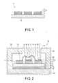
- Fig. 1 is a cross-sectional view showing the structure of a ceramic circuit board according to an embodiment of the present invention.
- Fig. 2 is a cross-sectional view showing an example of the structure of a power module including the ceramic circuit board according to the present invention.
- Embodiments of a ceramic circuit board of the present invention will now be described specifically with reference to the attached drawings.
- As shown in Tables 1 to 6, as ceramic substrates used in examples and comparative examples, a large number of silicon nitride (Si3N4) substrates, aluminum nitride (AIN) substrates, sialon (Si-Al-O-N) substrates, silicon carbide (SiC) substrates, and aluminum oxide (Al2O3) substrates that have a thickness of 0.625 to 1.2 mm were prepared. A blasting process and a polishing process were performed on a surface of each ceramic substrate for joining a clad member serving as a circuit layer so that the surface roughness (Ra) was controlled to be 1 µm.
- Subsequently, an Al alloy film having the composition and the thickness that were shown in Tables 1 to 6 was formed by vapor deposition on a part of each ceramic substrate for joining the circuit layer, the ceramic substrate having an adjusted surface roughness.
- On the other hand, an Al circuit plate and an Al-Si brazing material that had the compositions shown in Tables 1 to 6 were integrally joined so as to have a thickness ratio of 75:25 by rolling operation. Thus, clad members serving as the circuit layer were prepared. The thicknesses of the resulting clad members were determined to the values shown in Tables 1 to 6.
- Subsequently, each of the circuit layers composed of the clad member including the Al plate serving as the circuit plate and the Al-Si brazing material and each of the ceramic substrates having an Al alloy film (Examples) or an Al metal film (Comparative Example 1) thereon, which were prepared as described above, overlapped with each other. Each of the circuit layers and each of the ceramic substrates were then joined by heating to a temperature shown in Tables 1 to 6 in an atmosphere of a degree of vacuum shown in Tables 1 to 6 while a pressing load was applied so that the pressure was a value shown in Tables 1 to 6. Thereby, ceramic circuit boards of the examples and the comparative examples were produced.
- As shown in Fig. 1, a
ceramic circuit board 1 produced as described above has a structure in which acircuit layer 4 composed of a clad member including acircuit plate 2 made of an Al plate and an Al-Sibrazing material layer 3 is integrally joined on the surface of aceramic substrate 6 having an Al alloy film 5 (Examples) or an Al metal film (Comparative Example 1) thereon. - In order to evaluate the characteristics of the ceramic circuit boards of the examples and the comparative examples produced as described above, the following measurement tests were performed. First, a void ratio on the joint surface disposed under the circuit layer of each ceramic circuit board was measured with an ultrasonic flaw detector. The void ratio was determined by analyzing an image of voids that are present on the joint surface of a 20 mm square, the image being taken by the ultrasonic flaw detector. The void ratio was measured as a void area ratio per 20 mm square of the jointed area.
- A joint strength was measured as follows: The
circuit layer 4 of theceramic circuit board 1 of each example and each comparative example was pulled upward in the vertical direction in Fig. 1. The value calculated by dividing the tensile load when thecircuit layer 4 was peeled and separated from theceramic substrate 6 by the jointed area was defined as the joint strength. Tables 1 to 6 show the measured values, the specifications of the ceramic circuit boards, the joining conditions, and the like.


- As is apparent from the results shown in Tables 1 to 6, according to the ceramic circuit boards of the examples each prepared by forming an Al alloy film having a predetermined thickness on the surface of the ceramic substrate, even when the thickness of the Al alloy film is small to be less than 1 µm, the void area ratio was smaller than that of the comparative examples. This result showed that the diffusion and the ejection (the hillock phenomenon) of Al elements on the joint surface during joining by heating were effectively suppressed.
- Therefore, it was confirmed that the generation of voids in the joint surface could be effectively prevented and the joint strength was drastically increased and thus improved. Furthermore, since the thickness of the Al alloy film could be decreased to be less than 1 µm, the time required for depositing the Al alloy film by vapor deposition or the like could be reduced and the joining operation could be simplified. Therefore, it became clear that the joint assembly of the circuit board could be simplified to reduce the production cost drastically.
- On the other hand, according to the ceramic circuit board of Comparative Example 1 prepared by forming an Al metal layer on the surface of the ceramic substrate in advance, the diffusion of Al elements during joining by heating was significant and the ejection (the hillock phenomenon) of Al elements on the joint surface was not suppressed. It was reconfirmed that the joint strength was also drastically decreased in proportion to the sharp increase in the void area ratio.
- In addition, as shown in Comparative Examples 2 to 7, the results showed that when the composition of the Al alloy film (Comparative Examples 1 and 7), the joint temperature (Comparative Examples 1 and 5), the composition of Al-Si brazing material (Comparative Examples 2 and 4), the thickness of the Al alloy film (Comparative Example 3), the pressure during joining (Comparative Example 6), or the like were out of the preferred range specified in the present invention, the joint strength of the circuit layer and the void area property were decreased.
- Fig. 2 is a cross-sectional view showing an example of the structure of a power module including the ceramic circuit board according to an embodiment of the present invention. Namely, on the surface of an
Al circuit plate 2 of aceramic circuit board 1 disposed in apower module 10 of this embodiment, a semiconductor chip (semiconductor element) 11 including an IGBT (insulated gate bipolar transistor) serving as a power device is fixed withsolder 12. - The
Al circuit plate 2 is connected to an electrode terminal (not shown in the figure) for a collector and supplies thesemiconductor chip 11 with a collector voltage. Both ends of abonding wire 13 composed of a fine wire of a metal such as Al or Au are bonded to agate electrode 14 on thesemiconductor chip 11 and a metal film 15 on aceramic substrate 6, respectively, by using ultrasonic welding. Since the metal film 15 is connected to an electrode terminal (not shown in the figure) for a gate, thebonding wire 13 is electrically connected to the electrode terminal for the gate. Thus, a gate voltage is supplied from the electrode terminal for the gate through thebonding wire 13. - Further, both ends of a
bonding wire 16 are bonded to anemitter electrode 17 on thesemiconductor chip 11 and ametal film 18 on theceramic substrate 6, respectively, by using ultrasonic welding. Since anelectrode terminal 19 for an emitter is bonded on themetal film 18 withsolder 20, thebonding wire 16 is electrically connected to theelectrode terminal 19 for the emitter. Thus, an emitter voltage is supplied from theelectrode terminal 19 for the emitter through thebonding wire 16. - The bottom face of the
ceramic substrate 6 is joined on a metal substrate (heat sink) 24 with ametal film 22 andsolder 26 that are provided therebetween. Anouter shell case 28 composed of a plastic material or the like and themetal substrate 24 constitute apackage 29. Thesemiconductor chip 11, theceramic substrate 6, theAl circuit layer 2, themetal films 15 and 18, thebonding wires electrode terminal 19 for the emitter are sealed in thepackage 29 to constitute thesingle power module 10. Themetal substrate 24 can be formed as a component also serving as a heat sink, but radiation fins (heat sink) may be separately provided in addition to themetal substrate 24. Heat generated from thesemiconductor chip 11 is dissipated to the bottom face side of thesemiconductor chip 11 through themetal substrate 24, thereby cooling thesemiconductor chip 11. Thus, the operation and the function of thesemiconductor chip 11 are satisfactorily maintained. - According to the power module of the embodiment having the above-described structure, the generation of voids in the joint interface of the ceramic substrate can be effectively suppressed, and thus the joint strength of the metal member serving as the circuit layer can be increased. Consequently, a power module in which the heat resistance cycle characteristics can be drastically improved can be obtained and satisfactory reliability can be ensured.
- According to the ceramic circuit board, the method for producing the same, and the power module of the present invention, since an Al alloy film having a predetermined thickness is formed on the surface of a ceramic substrate, even when the thickness of this Al alloy film is small to be less than 1 µm, the diffusion and the ejection (the hillock phenomenon) of Al elements on the joint surface during joining by heating can be effectively suppressed, the generation of voids in the joint surface can be effectively prevented, and the joint assembly of the circuit board can be simplified thereby to reduce the production cost drastically
Claims (6)
- A ceramic circuit board prepared by integrally joining a circuit layer composed of a clad member including an Al plate and an Al-Si brazing material to a ceramic substrate, wherein a surface of the clad member adjacent to the Al-Si brazing material is joined to the ceramic substrate with an Al alloy film therebetween, the Al alloy film having a thickness of less than 1 µm and being provided on the surface of the ceramic substrate.
- The ceramic circuit board according to claim 1, wherein the ceramic substrate comprises an aluminum nitride sintered body, a silicon nitride sintered body, a silicon carbide sintered body, or a sialon sintered body.
- The ceramic circuit board according to claim 1, wherein the Al content of the Al-Si brazing material is 85 mass percent or more and the Si content of the Al-Si brazing material is in the range of 6 to 15 mass percent.
- The ceramic circuit board according to claim 1, wherein the Al alloy film comprises at least one rare earth element selected from Y, Sc, La, Ce, Nd, Sm, Gd, Tb, Dy, Er, Th, and Sr in an amount of 1 to 5 atomic percent.
- A method for producing a ceramic circuit board prepared by integrally joining a circuit layer composed of a clad member including an Al plate and an Al-Si brazing material to an Al alloy film, wherein said circuit layer composed of the clad member including the Al plate and the Al-Si brazing material and a ceramic substrate having the Al alloy film thereon overlap with each other, and said circuit layer and said ceramic substrate are then joined by heating at a temperature of 580°C to 630°C in an atmosphere of vacuum of 10-2 Pa or lower while a pressing load is applied to the overlapped the clad member and the ceramic substrate so that the pressure of the load is 2 kg/cm2 or more.
- A power module comprising:a ceramic circuit board prepared by integrally joining a circuit layer composed of a clad member including an Al plate and an Al-Si brazing material to a ceramic substrate, wherein a surface of said clad member adjacent to said Al-Si brazing material is joined to said ceramic substrate with an Al alloy film therebetween, said Al alloy film having a thickness of less than 1 µm and being provided on the surface of said ceramic substrate; .a semiconductor element mounted on said circuit layer; anda heat sink that dissipates heat generated from said semiconductor element via said ceramic circuit board.
Applications Claiming Priority (2)
| Application Number | Priority Date | Filing Date | Title |
|---|---|---|---|
| JP2003334190 | 2003-09-25 | ||
| PCT/JP2004/014528 WO2005032225A1 (en) | 2003-09-25 | 2004-09-27 | Ceramic circuit board, method for making the same, and power module |
Publications (3)
| Publication Number | Publication Date |
|---|---|
| EP1667508A1 true EP1667508A1 (en) | 2006-06-07 |
| EP1667508A4 EP1667508A4 (en) | 2008-03-12 |
| EP1667508B1 EP1667508B1 (en) | 2012-07-11 |
Family
ID=34386019
Family Applications (1)
| Application Number | Title | Priority Date | Filing Date |
|---|---|---|---|
| EP04773557A Expired - Lifetime EP1667508B1 (en) | 2003-09-25 | 2004-09-27 | Ceramic circuit board, method for making the same, and power module |
Country Status (5)
| Country | Link |
|---|---|
| US (1) | US7482685B2 (en) |
| EP (1) | EP1667508B1 (en) |
| JP (1) | JP4664816B2 (en) |
| CN (1) | CN100508698C (en) |
| WO (1) | WO2005032225A1 (en) |
Cited By (4)
| Publication number | Priority date | Publication date | Assignee | Title |
|---|---|---|---|---|
| WO2013171273A1 (en) * | 2012-05-16 | 2013-11-21 | Osram Gmbh | Electronic module, illuminating device and method for manufacturing such electronic module |
| EP2641997A4 (en) * | 2010-11-19 | 2017-12-20 | NHK Spring Co., Ltd. | Laminate and method for producing laminate |
| EP3166140A4 (en) * | 2014-07-04 | 2018-03-07 | Mitsubishi Materials Corporation | Substrate unit for power modules, and power module |
| WO2020074616A1 (en) * | 2018-10-11 | 2020-04-16 | Safran Electronics & Defense | Electronic assembly and pressure measurement device with improved durability |
Families Citing this family (24)
| Publication number | Priority date | Publication date | Assignee | Title |
|---|---|---|---|---|
| JP4207896B2 (en) * | 2005-01-19 | 2009-01-14 | 富士電機デバイステクノロジー株式会社 | Semiconductor device |
| JP2006253183A (en) * | 2005-03-08 | 2006-09-21 | Hitachi Ltd | Semiconductor power module |
| WO2007105361A1 (en) * | 2006-03-08 | 2007-09-20 | Kabushiki Kaisha Toshiba | Electronic component module |
| US8164176B2 (en) * | 2006-10-20 | 2012-04-24 | Infineon Technologies Ag | Semiconductor module arrangement |
| US7808100B2 (en) * | 2008-04-21 | 2010-10-05 | Infineon Technologies Ag | Power semiconductor module with pressure element and method for fabricating a power semiconductor module with a pressure element |
| CN102054826B (en) * | 2010-11-04 | 2013-01-09 | 嘉兴斯达微电子有限公司 | Novel baseplate-free power module |
| CN102593073B (en) * | 2011-01-11 | 2016-05-04 | 三菱综合材料株式会社 | Manufacture method, substrate for power module and the power module of substrate for power module |
| US8804339B2 (en) * | 2011-02-28 | 2014-08-12 | Toyota Motor Engineering & Manufacturing North America, Inc. | Power electronics assemblies, insulated metal substrate assemblies, and vehicles incorporating the same |
| DE102011103746A1 (en) * | 2011-05-31 | 2012-12-06 | Ixys Semiconductor Gmbh | Method for joining metal-ceramic substrates to metal bodies |
| JP5548167B2 (en) * | 2011-07-11 | 2014-07-16 | 日本発條株式会社 | Laminate and method for producing laminate |
| KR101659194B1 (en) * | 2011-12-20 | 2016-09-22 | 가부시끼가이샤 도시바 | Ceramic copper circuit board and semiconductor device employing same |
| JP6307832B2 (en) * | 2013-01-22 | 2018-04-11 | 三菱マテリアル株式会社 | Power module board, power module board with heat sink, power module with heat sink |
| CN103354221B (en) * | 2013-06-17 | 2016-02-03 | 苏州晶品光电科技有限公司 | For many ceramic layers pattern structure substrate of optics and electronic device |
| EP3358614B1 (en) * | 2015-09-28 | 2022-12-14 | Kabushiki Kaisha Toshiba | Circuit substrate and semiconductor device |
| CN105948825A (en) * | 2016-05-31 | 2016-09-21 | 佛山市康荣精细陶瓷有限公司 | Ceramic composite layer for brazing and preparation method thereof |
| US10399906B2 (en) | 2016-09-20 | 2019-09-03 | Ngk Insulators, Ltd. | Sialon sintered body, method for producing the same, composite substrate, and electronic device |
| CN106486865A (en) * | 2016-12-23 | 2017-03-08 | 深圳巴斯巴科技发展有限公司 | A kind of new and effective aluminum row |
| CN110226363B (en) * | 2017-03-30 | 2022-08-02 | 株式会社东芝 | Ceramic copper circuit board and semiconductor device using the same |
| WO2018207396A1 (en) * | 2017-05-11 | 2018-11-15 | 住友電気工業株式会社 | Semiconductor device |
| JP7346178B2 (en) * | 2019-09-05 | 2023-09-19 | 株式会社東芝 | semiconductor equipment |
| CN112447616A (en) * | 2020-11-19 | 2021-03-05 | 中车永济电机有限公司 | Novel integrated bottom plate structure of SiC IGBT device |
| US11737736B2 (en) * | 2021-06-11 | 2023-08-29 | GE Precision Healthcare LLC | Ultrasound imaging probe with improved heat dissipation |
| KR102617224B1 (en) * | 2021-06-25 | 2023-12-27 | 주식회사 아모센스 | Power module |
| WO2025177849A1 (en) * | 2024-02-22 | 2025-08-28 | 株式会社 東芝 | Ceramic circuit board and semiconductor device using same |
Family Cites Families (23)
| Publication number | Priority date | Publication date | Assignee | Title |
|---|---|---|---|---|
| FR2159632A5 (en) * | 1971-11-05 | 1973-06-22 | Thomson Csf | |
| JPS61291942A (en) * | 1985-06-19 | 1986-12-22 | Masaaki Naga | Alloy for metallizing |
| JPS61291943A (en) * | 1985-06-19 | 1986-12-22 | Masaaki Naga | Alloy for metallizing |
| EP0422558B1 (en) * | 1989-10-09 | 2001-03-28 | Mitsubishi Materials Corporation | Ceramic substrate used for fabricating electric or electronic circuit |
| US5213877A (en) * | 1991-05-02 | 1993-05-25 | Mitsubishi Materials Corporation | Ceramic substrate used for fabricating electric or electronic circuit |
| JP2884872B2 (en) * | 1991-12-17 | 1999-04-19 | 三菱マテリアル株式会社 | Semiconductor device mounting structure |
| JPH05277722A (en) * | 1992-03-18 | 1993-10-26 | Toshiba Corp | Material joining method |
| EP0661748A1 (en) * | 1993-12-28 | 1995-07-05 | Hitachi, Ltd. | Semiconductor device |
| DE69517248T2 (en) * | 1994-07-15 | 2000-10-12 | Mitsubishi Materials Corp., Tokio/Tokyo | Ceramic housing with high heat radiation |
| JPH0959074A (en) * | 1995-08-21 | 1997-03-04 | Ngk Spark Plug Co Ltd | Method for manufacturing joined body of ceramic member and aluminum member |
| JPH09110547A (en) * | 1995-10-11 | 1997-04-28 | Ngk Spark Plug Co Ltd | Method for manufacturing joined body of ceramic member and aluminum member |
| JP3152344B2 (en) * | 1996-08-22 | 2001-04-03 | 三菱マテリアル株式会社 | Ceramic circuit board |
| US6033787A (en) * | 1996-08-22 | 2000-03-07 | Mitsubishi Materials Corporation | Ceramic circuit board with heat sink |
| JP3346217B2 (en) * | 1997-04-04 | 2002-11-18 | カシオ計算機株式会社 | Wiring forming method and display device manufacturing method |
| US6261703B1 (en) * | 1997-05-26 | 2001-07-17 | Sumitomo Electric Industries, Ltd. | Copper circuit junction substrate and method of producing the same |
| JP3864282B2 (en) * | 1998-09-22 | 2006-12-27 | 三菱マテリアル株式会社 | Power module substrate, method for manufacturing the same, and semiconductor device using the substrate |
| JP3690944B2 (en) * | 1999-08-16 | 2005-08-31 | 電気化学工業株式会社 | Ceramic circuit board |
| JP4649027B2 (en) * | 1999-09-28 | 2011-03-09 | 株式会社東芝 | Ceramic circuit board |
| JP3932744B2 (en) * | 1999-11-16 | 2007-06-20 | 三菱マテリアル株式会社 | Manufacturing method of insulated circuit board for semiconductor mounting |
| JP4134537B2 (en) * | 2000-08-09 | 2008-08-20 | 三菱マテリアル株式会社 | Power module and power module with heat sink |
| JP2002111211A (en) * | 2000-09-28 | 2002-04-12 | Kyocera Corp | Ceramic wiring board |
| JP3648189B2 (en) * | 2001-09-28 | 2005-05-18 | 同和鉱業株式会社 | Metal-ceramic circuit board |
| JP2003163315A (en) * | 2001-11-29 | 2003-06-06 | Denki Kagaku Kogyo Kk | module |
-
2004
- 2004-09-27 US US10/572,961 patent/US7482685B2/en not_active Expired - Lifetime
- 2004-09-27 CN CNB2004800276374A patent/CN100508698C/en not_active Expired - Lifetime
- 2004-09-27 JP JP2005514299A patent/JP4664816B2/en not_active Expired - Lifetime
- 2004-09-27 WO PCT/JP2004/014528 patent/WO2005032225A1/en not_active Ceased
- 2004-09-27 EP EP04773557A patent/EP1667508B1/en not_active Expired - Lifetime
Cited By (6)
| Publication number | Priority date | Publication date | Assignee | Title |
|---|---|---|---|---|
| EP2641997A4 (en) * | 2010-11-19 | 2017-12-20 | NHK Spring Co., Ltd. | Laminate and method for producing laminate |
| WO2013171273A1 (en) * | 2012-05-16 | 2013-11-21 | Osram Gmbh | Electronic module, illuminating device and method for manufacturing such electronic module |
| EP3166140A4 (en) * | 2014-07-04 | 2018-03-07 | Mitsubishi Materials Corporation | Substrate unit for power modules, and power module |
| WO2020074616A1 (en) * | 2018-10-11 | 2020-04-16 | Safran Electronics & Defense | Electronic assembly and pressure measurement device with improved durability |
| FR3087264A1 (en) * | 2018-10-11 | 2020-04-17 | Safran Electronics & Defense | ELECTRONIC ASSEMBLY AND PRESSURE MEASURING DEVICE WITH IMPROVED DURABILITY |
| US11192776B2 (en) | 2018-10-11 | 2021-12-07 | Safran Electronics & Defense | Electronic assembly and pressure measurement device with improved durability |
Also Published As
| Publication number | Publication date |
|---|---|
| EP1667508B1 (en) | 2012-07-11 |
| US7482685B2 (en) | 2009-01-27 |
| JP4664816B2 (en) | 2011-04-06 |
| CN100508698C (en) | 2009-07-01 |
| US20070160858A1 (en) | 2007-07-12 |
| CN1857043A (en) | 2006-11-01 |
| JPWO2005032225A1 (en) | 2006-12-07 |
| WO2005032225A1 (en) | 2005-04-07 |
| EP1667508A4 (en) | 2008-03-12 |
Similar Documents
| Publication | Publication Date | Title |
|---|---|---|
| US7482685B2 (en) | Ceramic circuit board, method for making the same, and power module | |
| JP4969738B2 (en) | Ceramic circuit board and semiconductor module using the same | |
| KR101017333B1 (en) | Power semiconductor module | |
| JP5023165B2 (en) | Ceramic circuit board | |
| EP2296177B1 (en) | Method for manufacturing a power module substrate | |
| CN100573859C (en) | Semiconductor device and module and method of connecting semiconductor chip to ceramic substrate | |
| JP5957862B2 (en) | Power module substrate | |
| US20170309544A1 (en) | Semiconductor device and method for manufacturing semiconductor device | |
| EP3745453B1 (en) | Substrate for power module with heat sink, and power module | |
| WO1998008256A1 (en) | Silicon nitride circuit board and semiconductor module | |
| JP2004525503A (en) | Power module with improved transient thermal impedance | |
| JP2000265227A (en) | Composite materials, their production methods and applications | |
| EP3605601B1 (en) | Method for producing insulated circuit board with heat sink | |
| US11315868B2 (en) | Electronic-component-mounted module design to reduce linear expansion coefficient mismatches | |
| JPH06296084A (en) | Thermal conductor of high conductivity, wiring board provided therewith and manufacture thereof | |
| JP7143426B2 (en) | METAL-CERAMIC SUBSTRATE AND METHOD FOR MANUFACTURING METAL-CERAMIC SUBSTRATE | |
| JP3793562B2 (en) | Ceramic circuit board | |
| JP2003197824A (en) | Ceramic circuit board | |
| JP3934966B2 (en) | Ceramic circuit board | |
| JPH08102570A (en) | Ceramics circuit board | |
| JP2003092383A (en) | Power semiconductor device and heat sink thereof | |
| JP4476428B2 (en) | Aluminum nitride circuit board and manufacturing method thereof | |
| JP2554210B2 (en) | Metal bonded circuit board and electronic device using the same | |
| JP2000086368A (en) | Nitride ceramic substrate | |
| KR102930091B1 (en) | Semiconductor package |
Legal Events
| Date | Code | Title | Description |
|---|---|---|---|
| PUAI | Public reference made under article 153(3) epc to a published international application that has entered the european phase |
Free format text: ORIGINAL CODE: 0009012 |
|
| 17P | Request for examination filed |
Effective date: 20060313 |
|
| AK | Designated contracting states |
Kind code of ref document: A1 Designated state(s): DE FR GB |
|
| DAX | Request for extension of the european patent (deleted) | ||
| RBV | Designated contracting states (corrected) |
Designated state(s): DE FR GB |
|
| A4 | Supplementary search report drawn up and despatched |
Effective date: 20080208 |
|
| 17Q | First examination report despatched |
Effective date: 20100504 |
|
| REG | Reference to a national code |
Ref country code: DE Ref legal event code: R079 Ref document number: 602004038532 Country of ref document: DE Free format text: PREVIOUS MAIN CLASS: H05K0003380000 Ipc: H01L0023053000 |
|
| GRAP | Despatch of communication of intention to grant a patent |
Free format text: ORIGINAL CODE: EPIDOSNIGR1 |
|
| RIC1 | Information provided on ipc code assigned before grant |
Ipc: H05K 3/38 20060101ALN20120309BHEP Ipc: C04B 37/02 20060101ALI20120309BHEP Ipc: H01L 23/053 20060101AFI20120309BHEP |
|
| GRAS | Grant fee paid |
Free format text: ORIGINAL CODE: EPIDOSNIGR3 |
|
| GRAA | (expected) grant |
Free format text: ORIGINAL CODE: 0009210 |
|
| AK | Designated contracting states |
Kind code of ref document: B1 Designated state(s): DE FR GB |
|
| REG | Reference to a national code |
Ref country code: GB Ref legal event code: FG4D |
|
| REG | Reference to a national code |
Ref country code: DE Ref legal event code: R096 Ref document number: 602004038532 Country of ref document: DE Effective date: 20120906 |
|
| PLBE | No opposition filed within time limit |
Free format text: ORIGINAL CODE: 0009261 |
|
| STAA | Information on the status of an ep patent application or granted ep patent |
Free format text: STATUS: NO OPPOSITION FILED WITHIN TIME LIMIT |
|
| 26N | No opposition filed |
Effective date: 20130412 |
|
| REG | Reference to a national code |
Ref country code: DE Ref legal event code: R097 Ref document number: 602004038532 Country of ref document: DE Effective date: 20130412 |
|
| REG | Reference to a national code |
Ref country code: FR Ref legal event code: PLFP Year of fee payment: 13 |
|
| REG | Reference to a national code |
Ref country code: FR Ref legal event code: PLFP Year of fee payment: 14 |
|
| REG | Reference to a national code |
Ref country code: FR Ref legal event code: PLFP Year of fee payment: 15 |
|
| REG | Reference to a national code |
Ref country code: DE Ref legal event code: R084 Ref document number: 602004038532 Country of ref document: DE |
|
| REG | Reference to a national code |
Ref country code: GB Ref legal event code: 746 Effective date: 20180920 |
|
| PGFP | Annual fee paid to national office [announced via postgrant information from national office to epo] |
Ref country code: GB Payment date: 20230803 Year of fee payment: 20 |
|
| PGFP | Annual fee paid to national office [announced via postgrant information from national office to epo] |
Ref country code: FR Payment date: 20230808 Year of fee payment: 20 Ref country code: DE Payment date: 20230802 Year of fee payment: 20 |
|
| REG | Reference to a national code |
Ref country code: DE Ref legal event code: R071 Ref document number: 602004038532 Country of ref document: DE |
|
| PG25 | Lapsed in a contracting state [announced via postgrant information from national office to epo] |
Ref country code: GB Free format text: LAPSE BECAUSE OF EXPIRATION OF PROTECTION Effective date: 20240926 |
|
| REG | Reference to a national code |
Ref country code: GB Ref legal event code: PE20 Expiry date: 20240926 |
|
| PG25 | Lapsed in a contracting state [announced via postgrant information from national office to epo] |
Ref country code: GB Free format text: LAPSE BECAUSE OF EXPIRATION OF PROTECTION Effective date: 20240926 |