EP3745453B1 - Substrate for power module with heat sink, and power module - Google Patents
Substrate for power module with heat sink, and power module Download PDFInfo
- Publication number
- EP3745453B1 EP3745453B1 EP19743122.4A EP19743122A EP3745453B1 EP 3745453 B1 EP3745453 B1 EP 3745453B1 EP 19743122 A EP19743122 A EP 19743122A EP 3745453 B1 EP3745453 B1 EP 3745453B1
- Authority
- EP
- European Patent Office
- Prior art keywords
- heat sink
- power module
- layer
- substrate board
- bonding material
- Prior art date
- Legal status (The legal status is an assumption and is not a legal conclusion. Google has not performed a legal analysis and makes no representation as to the accuracy of the status listed.)
- Active
Links
- 239000000758 substrate Substances 0.000 title claims description 135
- 239000000463 material Substances 0.000 claims description 85
- 239000000919 ceramic Substances 0.000 claims description 49
- 229910052751 metal Inorganic materials 0.000 claims description 43
- 239000002184 metal Substances 0.000 claims description 43
- 229910052782 aluminium Inorganic materials 0.000 claims description 34
- XAGFODPZIPBFFR-UHFFFAOYSA-N aluminium Chemical compound [Al] XAGFODPZIPBFFR-UHFFFAOYSA-N 0.000 claims description 34
- 239000004065 semiconductor Substances 0.000 claims description 20
- RYGMFSIKBFXOCR-UHFFFAOYSA-N Copper Chemical compound [Cu] RYGMFSIKBFXOCR-UHFFFAOYSA-N 0.000 claims description 18
- 239000010949 copper Substances 0.000 claims description 18
- 229910052802 copper Inorganic materials 0.000 claims description 17
- 230000002093 peripheral effect Effects 0.000 claims description 11
- 229910000881 Cu alloy Inorganic materials 0.000 claims description 4
- 238000010438 heat treatment Methods 0.000 description 17
- 229920005989 resin Polymers 0.000 description 15
- 239000011347 resin Substances 0.000 description 15
- 238000000465 moulding Methods 0.000 description 13
- 238000005476 soldering Methods 0.000 description 7
- 229910052581 Si3N4 Inorganic materials 0.000 description 6
- 238000009792 diffusion process Methods 0.000 description 6
- 238000005304 joining Methods 0.000 description 6
- 239000007790 solid phase Substances 0.000 description 6
- PMHQVHHXPFUNSP-UHFFFAOYSA-M copper(1+);methylsulfanylmethane;bromide Chemical compound Br[Cu].CSC PMHQVHHXPFUNSP-UHFFFAOYSA-M 0.000 description 5
- 230000005855 radiation Effects 0.000 description 5
- 229910000838 Al alloy Inorganic materials 0.000 description 3
- PNEYBMLMFCGWSK-UHFFFAOYSA-N aluminium oxide Inorganic materials [O-2].[O-2].[O-2].[Al+3].[Al+3] PNEYBMLMFCGWSK-UHFFFAOYSA-N 0.000 description 3
- 238000004519 manufacturing process Methods 0.000 description 3
- HQVNEWCFYHHQES-UHFFFAOYSA-N silicon nitride Chemical compound N12[Si]34N5[Si]62N3[Si]51N64 HQVNEWCFYHHQES-UHFFFAOYSA-N 0.000 description 3
- 229910000679 solder Inorganic materials 0.000 description 3
- 230000035882 stress Effects 0.000 description 3
- 230000008646 thermal stress Effects 0.000 description 3
- VYPSYNLAJGMNEJ-UHFFFAOYSA-N Silicium dioxide Chemical compound O=[Si]=O VYPSYNLAJGMNEJ-UHFFFAOYSA-N 0.000 description 2
- 238000005219 brazing Methods 0.000 description 2
- 230000007547 defect Effects 0.000 description 2
- 230000000694 effects Effects 0.000 description 2
- 230000005496 eutectics Effects 0.000 description 2
- 238000011156 evaluation Methods 0.000 description 2
- 238000010030 laminating Methods 0.000 description 2
- 239000002075 main ingredient Substances 0.000 description 2
- 238000000034 method Methods 0.000 description 2
- 238000007789 sealing Methods 0.000 description 2
- 229910018125 Al-Si Inorganic materials 0.000 description 1
- 229910018520 Al—Si Inorganic materials 0.000 description 1
- 229910045601 alloy Inorganic materials 0.000 description 1
- 239000000956 alloy Substances 0.000 description 1
- 229910010293 ceramic material Inorganic materials 0.000 description 1
- 229910052681 coesite Inorganic materials 0.000 description 1
- 230000000052 comparative effect Effects 0.000 description 1
- 229910052593 corundum Inorganic materials 0.000 description 1
- 229910052906 cristobalite Inorganic materials 0.000 description 1
- 238000005516 engineering process Methods 0.000 description 1
- 239000003822 epoxy resin Substances 0.000 description 1
- 230000005669 field effect Effects 0.000 description 1
- 239000000945 filler Substances 0.000 description 1
- 239000011888 foil Substances 0.000 description 1
- 239000004519 grease Substances 0.000 description 1
- 238000009413 insulation Methods 0.000 description 1
- 229910044991 metal oxide Inorganic materials 0.000 description 1
- 150000004706 metal oxides Chemical class 0.000 description 1
- 238000012986 modification Methods 0.000 description 1
- 230000004048 modification Effects 0.000 description 1
- 230000001590 oxidative effect Effects 0.000 description 1
- 230000000149 penetrating effect Effects 0.000 description 1
- 229920000647 polyepoxide Polymers 0.000 description 1
- 238000004382 potting Methods 0.000 description 1
- 238000003825 pressing Methods 0.000 description 1
- 238000005086 pumping Methods 0.000 description 1
- 239000000377 silicon dioxide Substances 0.000 description 1
- 229910052682 stishovite Inorganic materials 0.000 description 1
- 238000001721 transfer moulding Methods 0.000 description 1
- 229910052905 tridymite Inorganic materials 0.000 description 1
- 229910001845 yogo sapphire Inorganic materials 0.000 description 1
Images


Classifications
-
- H—ELECTRICITY
- H01—ELECTRIC ELEMENTS
- H01L—SEMICONDUCTOR DEVICES NOT COVERED BY CLASS H10
- H01L23/00—Details of semiconductor or other solid state devices
- H01L23/34—Arrangements for cooling, heating, ventilating or temperature compensation ; Temperature sensing arrangements
- H01L23/36—Selection of materials, or shaping, to facilitate cooling or heating, e.g. heatsinks
- H01L23/373—Cooling facilitated by selection of materials for the device or materials for thermal expansion adaptation, e.g. carbon
- H01L23/3735—Laminates or multilayers, e.g. direct bond copper ceramic substrates
-
- C—CHEMISTRY; METALLURGY
- C04—CEMENTS; CONCRETE; ARTIFICIAL STONE; CERAMICS; REFRACTORIES
- C04B—LIME, MAGNESIA; SLAG; CEMENTS; COMPOSITIONS THEREOF, e.g. MORTARS, CONCRETE OR LIKE BUILDING MATERIALS; ARTIFICIAL STONE; CERAMICS; REFRACTORIES; TREATMENT OF NATURAL STONE
- C04B37/00—Joining burned ceramic articles with other burned ceramic articles or other articles by heating
- C04B37/02—Joining burned ceramic articles with other burned ceramic articles or other articles by heating with metallic articles
- C04B37/023—Joining burned ceramic articles with other burned ceramic articles or other articles by heating with metallic articles characterised by the interlayer used
- C04B37/026—Joining burned ceramic articles with other burned ceramic articles or other articles by heating with metallic articles characterised by the interlayer used consisting of metals or metal salts
-
- H—ELECTRICITY
- H01—ELECTRIC ELEMENTS
- H01L—SEMICONDUCTOR DEVICES NOT COVERED BY CLASS H10
- H01L23/00—Details of semiconductor or other solid state devices
- H01L23/12—Mountings, e.g. non-detachable insulating substrates
- H01L23/14—Mountings, e.g. non-detachable insulating substrates characterised by the material or its electrical properties
- H01L23/15—Ceramic or glass substrates
-
- H—ELECTRICITY
- H01—ELECTRIC ELEMENTS
- H01L—SEMICONDUCTOR DEVICES NOT COVERED BY CLASS H10
- H01L23/00—Details of semiconductor or other solid state devices
- H01L23/34—Arrangements for cooling, heating, ventilating or temperature compensation ; Temperature sensing arrangements
- H01L23/36—Selection of materials, or shaping, to facilitate cooling or heating, e.g. heatsinks
- H01L23/367—Cooling facilitated by shape of device
- H01L23/3677—Wire-like or pin-like cooling fins or heat sinks
-
- H—ELECTRICITY
- H01—ELECTRIC ELEMENTS
- H01L—SEMICONDUCTOR DEVICES NOT COVERED BY CLASS H10
- H01L23/00—Details of semiconductor or other solid state devices
- H01L23/34—Arrangements for cooling, heating, ventilating or temperature compensation ; Temperature sensing arrangements
- H01L23/36—Selection of materials, or shaping, to facilitate cooling or heating, e.g. heatsinks
- H01L23/373—Cooling facilitated by selection of materials for the device or materials for thermal expansion adaptation, e.g. carbon
- H01L23/3736—Metallic materials
-
- H—ELECTRICITY
- H01—ELECTRIC ELEMENTS
- H01L—SEMICONDUCTOR DEVICES NOT COVERED BY CLASS H10
- H01L23/00—Details of semiconductor or other solid state devices
- H01L23/34—Arrangements for cooling, heating, ventilating or temperature compensation ; Temperature sensing arrangements
- H01L23/42—Fillings or auxiliary members in containers or encapsulations selected or arranged to facilitate heating or cooling
- H01L23/433—Auxiliary members in containers characterised by their shape, e.g. pistons
- H01L23/4334—Auxiliary members in encapsulations
-
- H—ELECTRICITY
- H01—ELECTRIC ELEMENTS
- H01L—SEMICONDUCTOR DEVICES NOT COVERED BY CLASS H10
- H01L23/00—Details of semiconductor or other solid state devices
- H01L23/52—Arrangements for conducting electric current within the device in operation from one component to another, i.e. interconnections, e.g. wires, lead frames
- H01L23/538—Arrangements for conducting electric current within the device in operation from one component to another, i.e. interconnections, e.g. wires, lead frames the interconnection structure between a plurality of semiconductor chips being formed on, or in, insulating substrates
- H01L23/5386—Geometry or layout of the interconnection structure
-
- H—ELECTRICITY
- H01—ELECTRIC ELEMENTS
- H01L—SEMICONDUCTOR DEVICES NOT COVERED BY CLASS H10
- H01L23/00—Details of semiconductor or other solid state devices
- H01L23/562—Protection against mechanical damage
-
- C—CHEMISTRY; METALLURGY
- C04—CEMENTS; CONCRETE; ARTIFICIAL STONE; CERAMICS; REFRACTORIES
- C04B—LIME, MAGNESIA; SLAG; CEMENTS; COMPOSITIONS THEREOF, e.g. MORTARS, CONCRETE OR LIKE BUILDING MATERIALS; ARTIFICIAL STONE; CERAMICS; REFRACTORIES; TREATMENT OF NATURAL STONE
- C04B2237/00—Aspects relating to ceramic laminates or to joining of ceramic articles with other articles by heating
- C04B2237/02—Aspects relating to interlayers, e.g. used to join ceramic articles with other articles by heating
- C04B2237/12—Metallic interlayers
- C04B2237/121—Metallic interlayers based on aluminium
-
- C—CHEMISTRY; METALLURGY
- C04—CEMENTS; CONCRETE; ARTIFICIAL STONE; CERAMICS; REFRACTORIES
- C04B—LIME, MAGNESIA; SLAG; CEMENTS; COMPOSITIONS THEREOF, e.g. MORTARS, CONCRETE OR LIKE BUILDING MATERIALS; ARTIFICIAL STONE; CERAMICS; REFRACTORIES; TREATMENT OF NATURAL STONE
- C04B2237/00—Aspects relating to ceramic laminates or to joining of ceramic articles with other articles by heating
- C04B2237/02—Aspects relating to interlayers, e.g. used to join ceramic articles with other articles by heating
- C04B2237/16—Silicon interlayers
-
- C—CHEMISTRY; METALLURGY
- C04—CEMENTS; CONCRETE; ARTIFICIAL STONE; CERAMICS; REFRACTORIES
- C04B—LIME, MAGNESIA; SLAG; CEMENTS; COMPOSITIONS THEREOF, e.g. MORTARS, CONCRETE OR LIKE BUILDING MATERIALS; ARTIFICIAL STONE; CERAMICS; REFRACTORIES; TREATMENT OF NATURAL STONE
- C04B2237/00—Aspects relating to ceramic laminates or to joining of ceramic articles with other articles by heating
- C04B2237/30—Composition of layers of ceramic laminates or of ceramic or metallic articles to be joined by heating, e.g. Si substrates
- C04B2237/32—Ceramic
- C04B2237/36—Non-oxidic
- C04B2237/366—Aluminium nitride
-
- C—CHEMISTRY; METALLURGY
- C04—CEMENTS; CONCRETE; ARTIFICIAL STONE; CERAMICS; REFRACTORIES
- C04B—LIME, MAGNESIA; SLAG; CEMENTS; COMPOSITIONS THEREOF, e.g. MORTARS, CONCRETE OR LIKE BUILDING MATERIALS; ARTIFICIAL STONE; CERAMICS; REFRACTORIES; TREATMENT OF NATURAL STONE
- C04B2237/00—Aspects relating to ceramic laminates or to joining of ceramic articles with other articles by heating
- C04B2237/30—Composition of layers of ceramic laminates or of ceramic or metallic articles to be joined by heating, e.g. Si substrates
- C04B2237/40—Metallic
- C04B2237/402—Aluminium
-
- H—ELECTRICITY
- H01—ELECTRIC ELEMENTS
- H01L—SEMICONDUCTOR DEVICES NOT COVERED BY CLASS H10
- H01L2224/00—Indexing scheme for arrangements for connecting or disconnecting semiconductor or solid-state bodies and methods related thereto as covered by H01L24/00
- H01L2224/01—Means for bonding being attached to, or being formed on, the surface to be connected, e.g. chip-to-package, die-attach, "first-level" interconnects; Manufacturing methods related thereto
- H01L2224/26—Layer connectors, e.g. plate connectors, solder or adhesive layers; Manufacturing methods related thereto
- H01L2224/31—Structure, shape, material or disposition of the layer connectors after the connecting process
- H01L2224/32—Structure, shape, material or disposition of the layer connectors after the connecting process of an individual layer connector
- H01L2224/321—Disposition
- H01L2224/32151—Disposition the layer connector connecting between a semiconductor or solid-state body and an item not being a semiconductor or solid-state body, e.g. chip-to-substrate, chip-to-passive
- H01L2224/32221—Disposition the layer connector connecting between a semiconductor or solid-state body and an item not being a semiconductor or solid-state body, e.g. chip-to-substrate, chip-to-passive the body and the item being stacked
- H01L2224/32225—Disposition the layer connector connecting between a semiconductor or solid-state body and an item not being a semiconductor or solid-state body, e.g. chip-to-substrate, chip-to-passive the body and the item being stacked the item being non-metallic, e.g. insulating substrate with or without metallisation
-
- H—ELECTRICITY
- H01—ELECTRIC ELEMENTS
- H01L—SEMICONDUCTOR DEVICES NOT COVERED BY CLASS H10
- H01L2224/00—Indexing scheme for arrangements for connecting or disconnecting semiconductor or solid-state bodies and methods related thereto as covered by H01L24/00
- H01L2224/01—Means for bonding being attached to, or being formed on, the surface to be connected, e.g. chip-to-package, die-attach, "first-level" interconnects; Manufacturing methods related thereto
- H01L2224/34—Strap connectors, e.g. copper straps for grounding power devices; Manufacturing methods related thereto
- H01L2224/39—Structure, shape, material or disposition of the strap connectors after the connecting process
- H01L2224/40—Structure, shape, material or disposition of the strap connectors after the connecting process of an individual strap connector
- H01L2224/401—Disposition
- H01L2224/40135—Connecting between different semiconductor or solid-state bodies, i.e. chip-to-chip
- H01L2224/40137—Connecting between different semiconductor or solid-state bodies, i.e. chip-to-chip the bodies being arranged next to each other, e.g. on a common substrate
-
- H—ELECTRICITY
- H01—ELECTRIC ELEMENTS
- H01L—SEMICONDUCTOR DEVICES NOT COVERED BY CLASS H10
- H01L23/00—Details of semiconductor or other solid state devices
- H01L23/34—Arrangements for cooling, heating, ventilating or temperature compensation ; Temperature sensing arrangements
- H01L23/40—Mountings or securing means for detachable cooling or heating arrangements ; fixed by friction, plugs or springs
- H01L23/4006—Mountings or securing means for detachable cooling or heating arrangements ; fixed by friction, plugs or springs with bolts or screws
-
- H—ELECTRICITY
- H01—ELECTRIC ELEMENTS
- H01L—SEMICONDUCTOR DEVICES NOT COVERED BY CLASS H10
- H01L25/00—Assemblies consisting of a plurality of individual semiconductor or other solid state devices ; Multistep manufacturing processes thereof
- H01L25/03—Assemblies consisting of a plurality of individual semiconductor or other solid state devices ; Multistep manufacturing processes thereof all the devices being of a type provided for in the same subgroup of groups H01L27/00 - H01L33/00, or in a single subclass of H10K, H10N, e.g. assemblies of rectifier diodes
- H01L25/04—Assemblies consisting of a plurality of individual semiconductor or other solid state devices ; Multistep manufacturing processes thereof all the devices being of a type provided for in the same subgroup of groups H01L27/00 - H01L33/00, or in a single subclass of H10K, H10N, e.g. assemblies of rectifier diodes the devices not having separate containers
- H01L25/07—Assemblies consisting of a plurality of individual semiconductor or other solid state devices ; Multistep manufacturing processes thereof all the devices being of a type provided for in the same subgroup of groups H01L27/00 - H01L33/00, or in a single subclass of H10K, H10N, e.g. assemblies of rectifier diodes the devices not having separate containers the devices being of a type provided for in group H01L29/00
- H01L25/072—Assemblies consisting of a plurality of individual semiconductor or other solid state devices ; Multistep manufacturing processes thereof all the devices being of a type provided for in the same subgroup of groups H01L27/00 - H01L33/00, or in a single subclass of H10K, H10N, e.g. assemblies of rectifier diodes the devices not having separate containers the devices being of a type provided for in group H01L29/00 the devices being arranged next to each other
-
- H—ELECTRICITY
- H01—ELECTRIC ELEMENTS
- H01L—SEMICONDUCTOR DEVICES NOT COVERED BY CLASS H10
- H01L25/00—Assemblies consisting of a plurality of individual semiconductor or other solid state devices ; Multistep manufacturing processes thereof
- H01L25/18—Assemblies consisting of a plurality of individual semiconductor or other solid state devices ; Multistep manufacturing processes thereof the devices being of types provided for in two or more different subgroups of the same main group of groups H01L27/00 - H01L33/00, or in a single subclass of H10K, H10N
-
- H—ELECTRICITY
- H01—ELECTRIC ELEMENTS
- H01L—SEMICONDUCTOR DEVICES NOT COVERED BY CLASS H10
- H01L2924/00—Indexing scheme for arrangements or methods for connecting or disconnecting semiconductor or solid-state bodies as covered by H01L24/00
- H01L2924/15—Details of package parts other than the semiconductor or other solid state devices to be connected
- H01L2924/181—Encapsulation
Definitions
- the present invention relates to a heat sink-attached power module substrate board and a power module used for a semiconductor device controlling large current and high voltage.
- a power module substrate board used for a power module for example, known is a structure having a ceramic substrate board such as AlN (aluminum nitride), Al 2 O 4 (alumina), Si 3 N 4 (silicon nitride), or the like and a circuit layer bonded on one surface of the ceramic substrate board made of metal having excellent electric conductivity such as aluminum (Al), copper (Cu), and the like.
- a ceramic substrate board such as AlN (aluminum nitride), Al 2 O 4 (alumina), Si 3 N 4 (silicon nitride), or the like
- a circuit layer bonded on one surface of the ceramic substrate board made of metal having excellent electric conductivity such as aluminum (Al), copper (Cu), and the like.
- the power module substrates board of this kind there are cases in which a metal layer having high heat conductivity is formed on the other surface of the ceramic substrate board, and a heat sink (a heat-radiation layer) is bonded with the metal layer.
- the heat sink-attached power module substrate board on which the heat sink is joined is used in a state in which the heat sink is fixed on a cooler.
- a power module is manufactured by loading (mounting) semiconductor elements such as power elements on a surface (a top surface) of the circuit layer of the heat sink-attached power module substrate board composed as above described.
- the power module in which the semiconductor elements are mounted may be sealed with resin by potting, molding, or the like in order to maintain electric insulation, protect wires, and the like.
- a heat sink-attached power module substrate board is generally manufactured by joining a heat sink having high rigidity on a metal layer; and a circuit layer joined on one surface and the metal layer joined on the other surface of the ceramic substrate board are formed to have substantially a same thickness. Therefore, the heat sink-attached power module substrate has a difference of the rigidity at the upper and the lower with the ceramic substrate board therebetween; and a warp may be generated when it is heated in a mounting step of the semiconductors, or by temperature variation in usage environment, or the like.
- the warp is generated in the mounting step, bonding reliability is deteriorated on account of shifting of position of the semiconductor elements, distortion or cracks generated in joined parts of the semiconductor elements.
- the warp is generated in the usage environment, because of an outflow of thermal conductive grease between the heat sink and the cooler by pumping out from between the heat sink and the cooler, adhesiveness of the heat sink and the cooler is deteriorated, and thermal resistance is increased, so that thermal radiation property is hindered.
- Patent Document 1 it is described to compose a symmetric structure centering a ceramic substrate board with a heat sink made of aluminum having high rigidity, by forming a circuit layer as a laminated structure of a firs layer and a second layer and disposing the second layer made of aluminum having the high rigidity on the opposed surface of the ceramic substrate board.
- Patent Document 1 also describes that the second layer of the circuit layer and the heat sink are set to satisfy a range of a ratio (t1 ⁇ A1 ⁇ ⁇ 1)/(t2 ⁇ A2 ⁇ ⁇ 2) to be in not less than 0.85 and not more than 1.40, where the second layer of the circuit layer and the heat sink have thicknesses t1 and t2 (mm), joined areas A1 and A2 (mm 2 ), and yield strengths ⁇ 1 and ⁇ 2 (N/mm 2 ), so that the warp can be prevented by improving the symmetry centering the ceramic substrate board.
- Patent Document 2 describes that in a circuit layer composed of a plurality of small-circuit layers, the small-circuit layers have a structure of laminating a first layer and a second layer; and a heat sink (a heat radiation board) and the second layer are formed from material (copper or aluminum) of a same main ingredient, so that a symmetric structure centering a ceramic substrate board is composed.
- Patent document 2 describes that the symmetry of the circuit layer and the metal layer is further improved by providing non-joined part of the metal layer to the ceramic substrate board in non-joined area of the small-circuit layers.
- the symmetry structure centering the ceramic substrate board is composed by forming the heat sink (the heat radiation board) and the second layer of the circuit layer from material (copper or aluminum) of the same main ingredient: it is not possible to apply in a case of forming the circuit layer (the second layer) and the heat sink from different materials.
- the present invention is achieved in consideration of the above circumstances, and has an object to provide a heat sink-attached power module substrate board and a power module in which the circuit layer and the heat sink can be made of different materials, and the warp while being heated can be reduced.
- a heat sink-attached power module substrate board of the present invention is provided with a ceramic substrate board; a circuit layer joined on a first surface of the ceramic substrate board; a metal layer joined on a second surface of the ceramic substrate board; and a heat sink joined on the metal layer with heat radiation-side bonding material therebetween: in the heat sink-attached power module substrate board, the circuit layer is a laminated structure having a first layer joined on the first surface of the ceramic substrate board and a second layer joined on a surface of the first layer; the first layer and the metal layer are made of aluminum with purity of not less than 99.99% by mass, the second layer and the heat radiation-side bonding material are made of pure copper or copper alloy, the heat sink is made of aluminum of lower purity than the first layer and the metal layer, where A1 (mm 2 ) is a bonding area of the second layer and the first layer, t1 (mm) is an equivalent board thickness dividing a volume of the second layer by the bonding area A1, ⁇ 1 (N/mm 2 ) is an
- the circuit layer is the laminated structure of the first layer and the second layer
- copper material is used for the second layer of the circuit layer
- aluminum material is used for the heat sink
- the second layer is composed of copper having higher electric conductivity than aluminum.
- any of the bonding areas A1, A2, and A3, the equivalent board thicknesses t1, t2, and t3, the yield strengths ⁇ 1, ⁇ 2, and ⁇ 3 and the linear expansion coefficients ⁇ 1, ⁇ 2, and ⁇ 3 are values at 25°C (normal temperature).
- forms of the circuit layer and the heat sink are composed by various variations in a case in which the circuit layer is patterned by arranging a plurality of small-circuit layers and a case in which a fin is disposed on the heat sink. Also in those case, by evaluating the rigidity of the members by not only the yield strengths but a relational expression including the equivalent board thickness which is the volume of the members divided by the bonding area and the linear expansion coefficient of the members, the symmetry structure can be stably composed in the heat sink-attached power module substrate board having various forms for the symmetry of the rigidity and thermal stress between the second layer and the heat sink and the heat radiation-side bonding material, so that the warp can be reliably prevented.
- the stress generated at both surfaces of the ceramic substrate board while the heat sink-attached power module substrate board is heated is not easily biased, and the warp in the mounting step of the semiconductor elements and under the usage environment can be prevented from occurring. Accordingly, the bonding reliability of the power module can be improved, and good heat radiation property can be shown.
- an area of a top surface part of the heat sink on which the heat radiation-side bonding material is bonded be larger than an area of a bonded surface with the heat radiation-side bonding material.
- the top surface part of the heat sink By forming the top surface part of the heat sink to have the larger area than the bonded surface with the heat radiation-side bonding material, it is possible to provide a large bonding area to molding resin when the power module on which the semiconductor elements are mounted is sealed with the molding resin and the like. Accordingly, it is possible to improve the bonding reliability of the semiconductor elements and the heat sink-attached power module substrate board.
- the heat sink have a peripheral wall part standing at periphery of the top surface part toward the circuit layer and at least a part of the heat radiation-side bonding material be settled in a storing concave part surrounded by the top surface part and the peripheral wall part.
- a power module of the present invention is provided with the heat sink-attached power module substrate board and a semiconductor element mounted on a surface of the circuit layer.
- the warp while being heated can be reduced, so that defects of the mounting step of the semiconductor elements can be removed, the warp while heat cycles (hot-cold cycles), and the bonding reliability can be improved.
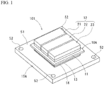
- FIG. 1 and FIG. 2 show a heat sink-attached power module substrate board 101 of a first embodiment.
- the heat sink-attached power module substrate board 101 is provided with a power module substrate board 10A and a heat sink 15A bonded on the power module substrate board 10A with a heat radiation-side bonding material 14 therebetween.
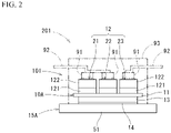
- a power module 201 is manufactured by mounting elements 91 such as semiconductor elements and the like on a surface of the heat sink-attached power module substrate board 101 as shown in FIG. 2 .
- the elements 91 and the heat sink-attached power module substrate board 101 are resin-shielded by molding resin 93 consisting of epoxy resin or the like, and the power module 201 is used in a state of being fixed by pressing an exposed surface of the power module 201 (an exposed surface of the heat sink 15A) of the power module 201 against a surface of another member such as a cooler or the like.
- the power module substrate board 10A is provided with one ceramic substrate board 11, a circuit layer 12 joined on a first surface of the ceramic substrate board 11, and one metal layer 13 joined on a second surface of the ceramic substrate board 11 as shown in FIG. 1 and FIG. 2 .
- the ceramic substrate board 11 is made of ceramic material such as AlN (aluminum nitride), Si 3 N 4 (silicon nitride), Al 2 O 3 (alumina) or the like, for example.
- the circuit layer 12 consists of a plurality of small-circuit layers 21 to 23 as shown in FIG. 1 and FIG. 2 .
- the small-circuit layers 21 to 23 are joined on the first surface of the ceramic substrate board 11 with an interval therebetween.
- the small-circuit layers 21 to 23 composing the circuit layer 12 have a laminated structure having first layers 121 joined on a surface (the first surface) of the ceramic substrate board 11 and second layers 122 joined on a surface of the circuit layer 121 (an opposed surface to the ceramic substrate board 11).
- the first layers 121 are formed of aluminum of purity not less than 99.99% by mass (so-called 4N aluminum) and joined on the first surface of the ceramic substrate board 11 by brazing material.
- the second layers 122 are formed of pure copper or copper alloy and joined on the first layers 121 made of aluminum by solid phase diffusion bonding.
- the metal layer 13 is formed of aluminum with purity of not less than 99.99% by mass same as the first layers 121 of the circuit layer 12 and joined on the second surface (an opposed side of the circuit layer 12) of the ceramic substrate board 11 by brazing material.
- the heat sink 15A is joined on the surface (the opposed surface to the ceramic substrate board 11) of the metal layer 13 with the heat radiation-side bonding material 14 therebetween.
- the heat radiation-side bonding material 14 is made of copper or copper alloy same as the second layers 122 of the circuit layer 12 and joined to the metal layer 13 and the heat sink 15A by solid phase diffusion bonding.
- the heat sink 15A is formed of aluminum with lower purity than the first layers 121 of the circuit layer 12 and the metal layer 13; for example by JIS standard, it is formed of so-called 3N aluminum with purity of not less than 99.90% by mass, so-called 2N aluminum with purity of not less than 99.0% by mass (e.g., A1050 and so forth), and aluminum alloys such as A3003, A6063, A5052, and the like.
- the heat sink 15A has a top surface part 51 of a rectangle flat board shape.
- the heat radiation-side bonding material 14 is joined on the top surface part 51.
- the metal layer 13 of the power module substrate board 10A is joined on the top surface part 51 with the heat radiation-side bonding material 14 therebetween.
- An upper surface of the top surface part 51 is formed to be larger than a bonded surface to the heat radiation-side bonding material 14.
- Mounting holes 52 penetrating in a thickness direction are formed at four corners in a surface direction of the top surface part. It is possible to assemble the heat sink-attached power module substrate board 101 into another member using the mounting holes 52 of the heat sink 15A by screwing and so forth.
- a form of the heat sink 15A is not especially limited, but other than a flat board form shown in FIG. 1 and FIG. 2 , suitable forms such as a form in which a plurality of pin fins are integrally formed, a form in which belt fins which are parallel to each other are integrally formed, and the like are applicable.
- a board thickness of the ceramic substrate board 11 made of Si 3 N 4 (silicon nitride) is 0.2 mm to 1.5 mm; a board thickness of the first layers 121 made of aluminum with purity of not less than 99.99% by mass (so-called 4N aluminum) is 0.1 mm to 2.5 mm; and a board thickness of the metal layer 13 is 0.1 mm to 2.5 mm.
- Aboard thickness of the second layer 122 made of oxygen-free copper (C1020) is 0.1 mm to 4.0 mm; and a board thickness of the heat radiation-side bonding material 14 is 0.05 mm to 2.0 mm.
- a board thickness of the top surface part 51 of the heat sink 15A made of A6063 aluminum alloy is 0.5 mm to 3.0 mm. However, these dimensions are not limited to the above value ranges.
- the heat sink-attached power module substrate board 101 composed as above is adjusted to be a relation in which a ratio (A1 ⁇ t1 ⁇ ⁇ 1 ⁇ ⁇ 1)/ ⁇ (A2 ⁇ t2 ⁇ ⁇ 2 ⁇ ⁇ 2) + (A3 ⁇ t3 ⁇ ⁇ 3 ⁇ ⁇ 3) ⁇ at 25°C (room temperature) is not less than 0.70 and not more than 1.30;
- A1 (mm 2 ) is a bonding area of the second layers 122 and the first layers 121 in the circuit layer 12
- t1 (mm) is an equivalent board thickness dividing a volume of the second layers by the bonding area A1
- ⁇ 1 (N/mm 2 ) is an yield strength of the second layers 122
- ⁇ 1 (/K) is a linear expansion coefficient of the second layers 122;
- A2 (mm 2 ) is a bonding area of the heat radiation-side bonding material 14 and the metal layer 13
- t2 (mm) is an equivalent board thickness
- the bonding areas A1, A2, and A3, the equivalent board thicknesses t1, t2, and t3, the yield stresses ⁇ 1, ⁇ 2, and ⁇ 3, and the linear expansion coefficients ⁇ 1, ⁇ 2, and ⁇ 3 are the values at 25°C (normal temperature).
- the bonding area A1 of the first layers 121 and the second layers 122 in the relational expression of the above ratio is a total sum (a11 + a12 + a13) of bonding areas a11 to a13 of the three first layers 121 and the three second layers 122 in the small-circuit layers 21 to 23 composing the circuit layer 12, since the circuit layer 12 is formed from the plurality of small-circuit layers 21 to 23, as shown in FIG. 4 .
- the equivalent board thickness t1 of the second layer 122 is a value of a total volume V1 of the three second layers 122 divided by the bonding area A1 in the small-circuit layers 21 to 23.
- a total volume V1 (v11 + v12 + v13) of the second layers 122
- the heat radiation-side bonding material 14 is composed of one as shown in FIG. 4 , a volume V2 of the heat radiation-side bonding material 14 is single volume and the bonding area A2 of the heat radiation-side bonding material 14 and the metal layer 13 is single area. Accordingly, the equivalent board thickness t2 of the heat radiation-side bonding material 14 is (V2/A2).
- the mounting holes 52 are formed in the top surface part 51, so that a space volume of the mounting holes 52 is not included in the volume V3 of the heat sink 15A.
- the power module 201 is manufactured by installing the elements 91 complying with required functions on the heat sink-attached power module substrate board 101 composed as above described.
- the elements 91 are electric parts having semiconductors, selected from various semiconductors such as IGBT (Insulated Gate Bipolar transistor), MOSFET (Metal Oxide Semiconductor Field Effect Transistor), FWD (Free Wheeling Diode), and the like.
- IGBT Insulated Gate Bipolar transistor
- MOSFET Metal Oxide Semiconductor Field Effect Transistor
- FWD Free Wheeling Diode
- the elements 91 are provided with an upper electrode part at the upper part and lower electrode part at the lower part, and mounted on the upper surface of the circuit layer 12 (the second layers 122) by joining the lower electrode part on the upper surface of the circuit layer 12 by soldering or the like.
- the upper electrode parts of the elements 91 are connected to circuit electrode parts or the like of the circuit layer 12 by lead frames 92 and the like joined by soldering and the like.
- the elements 91 and the heat sink-attached power module substrate board 101 are integrated by resin sealing by the molding resin 93 excepting the back surface side of the metal layer 13 in the power module 201 on which the elements 91 are mounted.
- the molding resin 93 epoxy-type resin including SiO 2 filler and the like can be used for example; and it is formed by transfer molding for example.
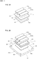
- the heat sink-attached power module substrate board 101 is manufactured by joining the ceramic substrate board 11, the first layers 121 of the circuit layer 12, and the metal layer 13 (a first bonding step), and then joining the second layers 122 on the surface of the first layers 121, joining the heat radiation-side bonding material 14 on the surface of the metal layer 13, and further joining the heat sink 15A on the surface of the heat radiation-side bonding material 14 (a second bonding step).
- first layer aluminum boards 121a which will be the first layers 121 of the circuit layer 12 are laminated on one surface of the ceramic substrate board 11 with soldering material 41 therebetween; and on the other surface, a metal layer aluminum board 13a which will be the metal layer 13 is laminated with the soldering material 41 therebetween.
- a laminated body of these is pressed in a laminating direction and heated to bonding temperature under vacuum atmosphere; so that the layers are bonded by the soldering material 41 and a joined body 30 formed integral is obtained.
- soldering material of alloy of Al-Si type or the like
- a condition of solder bonding is as follows: a pressurizing forth is 0.1 MPa to 1.0 MPa; heating temperature is 630°C to 650°C; and this pressurizing and heating state is maintained for 10 minutes to 50 minutes.
- second layer copper boards 122a which will be the second layers 122 are laminated on the first layers 121 of the joined body 30 obtained from the first bonding step, and the metal layer 13 is laminated on the heat sink 15A with a bonding board 14a which will be the heat radiation-side bonding material 14 therebetween.
- the laminated body of these is heated to the bonding temperature in the pressed state under vacuum atmosphere, so that the first layers 121 and the second layers 122, the metal layer 13 and the heat radiation-side bonding material 14, and the heat radiation-side bonding material 14 and the heat sink 15A are joined by the solid phase diffusion respectively.
- the pressurizing and heating state of the pressurizing force 0.5 MPa to 2.0 MPa and the heating temperature 500°C to 540°C is maintained for 30 minutes to 120 minutes.
- the first layers 121 and the second layers 122, the metal layer 13 and the heat radiation-side bonding material 14, and the heat radiation-side bonding material 14 and the heat sink 15A are joined at the same time: the heat sink-attached power module substrate board 101 shown in FIG. 1 is obtained.
- the respective bonding surfaces between the first layers 121 and the second layers 122, the metal layer 13 and the heat radiation-side bonding material 14, and the heat radiation-side bonding material 14 and the heat sink 15A are flattened and smoothed by removing scratches in advance and then bonded by the solid phase diffusion.
- Preferable heating temperature of vacuum heating in the solid phase diffusion bonding is a range not less than eutectic temperature of aluminum and copper minus 5°C and less than the eutectic temperature.
- the heat sink-attached power module substrate board 101 is composed as above described, copper material is used for the second layers 122 of the circuit layer 12, aluminum material is used for the heat sink 15A: the second layers 122 are composed from copper having higher electric conductivity than aluminum.
- the symmetry structure centering the ceramic substrate board 11 is composed of the aluminum material having low purity aluminum and high rigidity: i.e., the aluminum material having the high yield strength for the heat sink 15A, and in the combination of these, adjusting the ratio (A1 ⁇ t1 ⁇ ⁇ 1 ⁇ ⁇ 1)/ ⁇ (A2 ⁇ t2 ⁇ ⁇ 2 ⁇ ⁇ 2) + (A3 ⁇ t3 ⁇ ⁇ 3 ⁇ ⁇ 3) ⁇ into the range not less than 0.70 and not more than 1.30 at 25°C (room temperature).
- the rigidity of the members composing the heat sink-attached power module substrate board 101 is evaluated from not only the yield strength, but the relational expression (the ratio) considering the equivalent board thickness which is the volume of the members divided by the bonding area and the linear expansion coefficient of the members. Therefore, as the heat sink-attached power module substrate board 101, even in a structure in which the plurality of small-circuit layers 21 to 23 are aligned so as to pattern the circuit layer 12, it is easy to compose the symmetry structure centering the ceramic substrate board 11, and it is possible to prevent the warp resulting from heating.
- the inner stress at both the surfaces of the ceramic substrate board 11 resulting from heating the heat sink-attached power module substrate board 101 and the like is not biased, and the warp can be prevented in the mounting process of the elements 91 and the usage environment.
- the bonding reliability of the power module 201 is improved and good heat radiation property can be performed.
- the bonding area to the molding resin 93 can be broadly provided when sealing the power module 201 on which the elements 91 are mounted by the molding resin 93 and the like. Accordingly, the bonding reliability of the elements 91 and the heat sink-attached power module substrate board 101 can be improved.
- the heat sink 15A is composed from the flat board-like top surface part 51: however, the present invention includes a structure as a heat sink-attached power module substrate board 102 (a power module 202) of a second embodiment shown in FIG. 5 and FIG. 6 , provided with a heat sink 15B in which a plurality of pin fins 53 are disposed.
- An explanation of the second embodiment is simplified by denoting the same components as in the first embodiment by the same references.
- the heat sink 15B has a form in which the pin fins 53 stands on the lower surface of the top surface part 51 as shown in FIG. 5 and FIG. 6 .
- the whole volume V3 is a value including the top surface part 51 and the pin fins 53; the equivalent board thickness t3 of the heat sink 15B is obtained from the volume V3.
- the heat sink-attached power module substrate board 102 composed as above is adjusted to have a relation in which the ratio (A1 ⁇ t1 ⁇ ⁇ 1 ⁇ ⁇ 1)/ ⁇ (A2 ⁇ t2 ⁇ ⁇ 2 ⁇ ⁇ 2) + (A3 ⁇ t3 ⁇ ⁇ 3 ⁇ ⁇ 3) ⁇ at 25°C (room temperature) is not less than 0.70 and not more than 1.30.
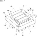
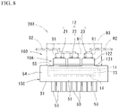
- FIG. 7 and FIG. 8 shows a heat sink-attached power module substrate board 103 (a power module 203) of a third embodiment.
- the same elements as in the first embodiment and the second embodiment are denoted by the same reference symbols and explanations are omitted also in this third embodiment.
- a heat sink 15C has a peripheral wall part 54 standing toward the circuit layer 12 from a periphery of the top surface part 51, and a storing concave part 55 is provided on a top surface of the heat sink 15C to be surrounded by the top surface part 51 and the peripheral wall part 54.
- the power module substrate board 10A and the heat sink 15C are joined with the heat radiation-side bonding material 14 therebetween. At least a part of the heat radiation-side bonding material 14 is stored in the storing concave part 55 of the heat sink 15C.
- the heat radiation-side bonding material 14, the metal layer 13 and the ceramic substrate board 11, and a part of the first layers 121 are stored inside the storing concave part 55.
- the whole volume V3 is a value including the top surface part 51, the pin fins 53, and the peripheral wall part 54; the equivalent board thickness t3 of the heat sink 15C is obtained from the volume V3.
- the heat sink-attached power module substrate board 103 composed as above is adjusted to have the relation in which the ratio (A1 ⁇ t1 ⁇ ⁇ 1 ⁇ ⁇ 1)/ ⁇ (A2 ⁇ t2 ⁇ ⁇ 2 ⁇ ⁇ 2) + (A3 ⁇ t3 ⁇ ⁇ 3 ⁇ ⁇ 3) ⁇ at 25°C (room temperature) is not less than 0.70 and not more than 1.30.
- the heat sink-attached power module substrate board 103 since the storing concave part 55 surrounded by the peripheral wall part 54 is formed in the heat sink 15C, it is possible to provide a larger bonding area to the molding resin 93 when the power module 203 on which the elements 91 are mounted is sealed by the molding resin 93 or the like. Accordingly, it is possible to improve the bonding reliability of the elements 91 and the heat sink-attached power module substrate board 103.
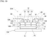
- FIG. 9 A heat sink-attached power module substrate board 104 (a power module 204) of a fourth embodiment is shown in FIG. 9 and FIG. 10 .
- the same elements as in the above-mentioned first to third embodiments are denoted by the same reference symbols and explanations are omitted also in this third embodiment.
- terminal parts 123 are formed integrally with the second layers 122 of the circuit layer 12 to project from the first layers 121.
- lead frames 94 are connected by solder or the like for external connection.
- the whole volume V1 is a value including the terminal parts 123, and the equivalent board thickness t1 of the second layers 122 is obtained from this volume V1.
- the heat sink-attached power module substrate board 104 composed as above is adjusted to have the relation in which the ratio (A1 ⁇ t1 ⁇ ⁇ 1 ⁇ ⁇ 1)/ ⁇ (A2 ⁇ t2 ⁇ ⁇ 2 ⁇ ⁇ 2) + (A3 ⁇ t3 ⁇ ⁇ 3 ⁇ ⁇ 3) ⁇ at 25°C (room temperature) is not less than 0.70 and not more than 1.30.
- the heat sink-attached power module substrate board 104 composed of the circuit layer 12 and the heat sink 15A with the various forms is also evaluated not only by the rigidity of the members but by the relational expression including the equivalent board thickness which is the volume of the members divided by the bonding area and the linear expansion coefficient of the members, so it is possible to compose the symmetry structure centering the ceramic substrate board 11 and prevent the warp resulting from heating.
- the ceramic substrate board made of AlN with a board thickness 0.635 mm and the first layer and the metal layer made of 4N-Al with a board thickness 0.6 mm were prepared as members composing samples of Invention Examples 1 to 10 and Comparative Examples 1 to 3.
- Tables 1 to 3 show the material, the equivalent board thickness, the bonding area, the linear expansion coefficient (CTE), and the yield strength, regarding the second layer of the circuit layer, the heat radiation-side bonding material, and the heat sink.
- EMBODIMENT denotes that the second layer and the heat sink of the respective samples were formed into forms (the shapes) of which of the embodiments.
- RATIO in Table 4 denotes the ratio (A1 ⁇ t1 ⁇ ⁇ 1 ⁇ ⁇ 1)/ ⁇ (A2 ⁇ t2 ⁇ ⁇ 2 ⁇ ⁇ 2) + (A3 ⁇ t3 ⁇ ⁇ 3 ⁇ ⁇ 3) ⁇ at 25°C.
- "YIELD STRENGTH” in Tables 1 to 3 was measured as the yield strength at 25°C by the method based on JIS Standard G0567:2012.
- the samples of the heat sink-attached power module substrate board were made by bonding these according to the manufacturing method described in the first embodiment. Warp amount (initial warp) at normal temperature (25°C) after bonding and warp amount when heated to 280°C (heated warp) were measured respectively for the obtained samples.
- the warp amount was measured for a change of the flatness at a center part (an area of 40 mm ⁇ 40 mm) of a back surface of the heat sink by a moire-type three-dimensional shape measuring device. If a difference between the initial warp and the heating warp was not more than 150 ⁇ m, the evaluation was "A" as good for the warp amount is small; or if the difference was more than 150 ⁇ m, the evaluation was "B" as bad for the warp amount was large. The results are shown in Table 4.
- the warp resulting from heating is reduced and defects in the mounting step of the semiconductor elements are removed, and the warp resulting from the temperature cycles (cold/hot cycles) can be reduced and the bonding reliability is improved.
Description
- The present invention relates to a heat sink-attached power module substrate board and a power module used for a semiconductor device controlling large current and high voltage.
- As a power module substrate board used for a power module, for example, known is a structure having a ceramic substrate board such as AlN (aluminum nitride), Al2O4 (alumina), Si3N4 (silicon nitride), or the like and a circuit layer bonded on one surface of the ceramic substrate board made of metal having excellent electric conductivity such as aluminum (Al), copper (Cu), and the like.
- In the power module substrates board of this kind, there are cases in which a metal layer having high heat conductivity is formed on the other surface of the ceramic substrate board, and a heat sink (a heat-radiation layer) is bonded with the metal layer. The heat sink-attached power module substrate board on which the heat sink is joined is used in a state in which the heat sink is fixed on a cooler.
- A power module is manufactured by loading (mounting) semiconductor elements such as power elements on a surface (a top surface) of the circuit layer of the heat sink-attached power module substrate board composed as above described. The power module in which the semiconductor elements are mounted may be sealed with resin by potting, molding, or the like in order to maintain electric insulation, protect wires, and the like.
- A heat sink-attached power module substrate board is generally manufactured by joining a heat sink having high rigidity on a metal layer; and a circuit layer joined on one surface and the metal layer joined on the other surface of the ceramic substrate board are formed to have substantially a same thickness. Therefore, the heat sink-attached power module substrate has a difference of the rigidity at the upper and the lower with the ceramic substrate board therebetween; and a warp may be generated when it is heated in a mounting step of the semiconductors, or by temperature variation in usage environment, or the like.
- If the warp is generated in the mounting step, bonding reliability is deteriorated on account of shifting of position of the semiconductor elements, distortion or cracks generated in joined parts of the semiconductor elements. In a case in which the warp is generated in the usage environment, because of an outflow of thermal conductive grease between the heat sink and the cooler by pumping out from between the heat sink and the cooler, adhesiveness of the heat sink and the cooler is deteriorated, and thermal resistance is increased, so that thermal radiation property is hindered.
- For this reason, it is required that the warp is small in the heat sink-attached power module substrate board: technology of reducing the warp of the heat sink-attached power module substrate board is proposed in the past.
- For example, in
Patent Document 1, it is described to compose a symmetric structure centering a ceramic substrate board with a heat sink made of aluminum having high rigidity, by forming a circuit layer as a laminated structure of a firs layer and a second layer and disposing the second layer made of aluminum having the high rigidity on the opposed surface of the ceramic substrate board. -
Patent Document 1 also describes that the second layer of the circuit layer and the heat sink are set to satisfy a range of a ratio (t1 × A1 × σ1)/(t2 × A2 × α2) to be in not less than 0.85 and not more than 1.40, where the second layer of the circuit layer and the heat sink have thicknesses t1 and t2 (mm), joined areas A1 and A2 (mm2), and yield strengths σ1 and σ2 (N/mm2), so that the warp can be prevented by improving the symmetry centering the ceramic substrate board. - Patent Document 2 describes that in a circuit layer composed of a plurality of small-circuit layers, the small-circuit layers have a structure of laminating a first layer and a second layer; and a heat sink (a heat radiation board) and the second layer are formed from material (copper or aluminum) of a same main ingredient, so that a symmetric structure centering a ceramic substrate board is composed.
- Patent document 2 describes that the symmetry of the circuit layer and the metal layer is further improved by providing non-joined part of the metal layer to the ceramic substrate board in non-joined area of the small-circuit layers.
-
- Patent Document 1:
Japanese Unexamined Patent Application, First Publication No. 2015-216370 - Patent Document 2:
Japanese Unexamined Patent Application, First Publication No. 2017-73483 - As described above, in order to reduce the warp in the heat sink-attached power module substrate board while being heated, composing the symmetry structure centering the ceramic substrate board is carried out. However, in
Patent Document 1 and Patent Document 2, the symmetry structure centering the ceramic substrate board is composed by forming the heat sink (the heat radiation board) and the second layer of the circuit layer from material (copper or aluminum) of the same main ingredient: it is not possible to apply in a case of forming the circuit layer (the second layer) and the heat sink from different materials. - The present invention is achieved in consideration of the above circumstances, and has an object to provide a heat sink-attached power module substrate board and a power module in which the circuit layer and the heat sink can be made of different materials, and the warp while being heated can be reduced.
- A heat sink-attached power module substrate board of the present invention is provided with a ceramic substrate board; a circuit layer joined on a first surface of the ceramic substrate board; a metal layer joined on a second surface of the ceramic substrate board; and a heat sink joined on the metal layer with heat radiation-side bonding material therebetween: in the heat sink-attached power module substrate board, the circuit layer is a laminated structure having a first layer joined on the first surface of the ceramic substrate board and a second layer joined on a surface of the first layer; the first layer and the metal layer are made of aluminum with purity of not less than 99.99% by mass, the second layer and the heat radiation-side bonding material are made of pure copper or copper alloy, the heat sink is made of aluminum of lower purity than the first layer and the metal layer, where A1 (mm2) is a bonding area of the second layer and the first layer, t1 (mm) is an equivalent board thickness dividing a volume of the second layer by the bonding area A1, σ1 (N/mm2) is an yield strength of the second layer, and α1 (/K) is a linear expansion coefficient of the second layer; where A2 (mm2) is a bonding area of the heat radiation-side bonding material and the metal layer, t2 (mm) is an equivalent board thickness dividing a volume of the heat radiation-side bonding material by the bonding area A2, σ2 (N/mm2) is an yield strength of the heat radiation-side bonding material, and α2 (/K) is a linear expansion coefficient of the heat radiation-side bonding material; and where A3 (mm2) is a bonding area of the heat sink and the heat radiation-side bonding material, t3 (mm) is an equivalent board thickness dividing a volume of the heat sink by the bonding area A3, σ3 (N/mm2) is an yield strength of the heat sink, and α3 (/K) is a linear expansion coefficient of the heat sink, a ratio (A1 × t1 × σ1 × α1)/{(A2 × t2 × σ2 × α2) + (A3 × t3 × σ3 × α3)} at 25°C is not less than 0.70 and not more than 1.30.
- In this heat sink-attached power module substrate board, the circuit layer is the laminated structure of the first layer and the second layer, copper material is used for the second layer of the circuit layer, aluminum material is used for the heat sink, and the second layer is composed of copper having higher electric conductivity than aluminum. By using the aluminum material with low purity of aluminum and high rigidity, i.e., high yield strength for the heat sink and using the copper material for the heat radiation-side bonding material between the metal layer and the heat sink, and by adjusting the above-mentioned ratio at 25°C in the above-mentioned range in the combination, the symmetry structure centering the ceramic substrate board is composed.
- Any of the bonding areas A1, A2, and A3, the equivalent board thicknesses t1, t2, and t3, the yield strengths σ1, σ2, and σ3 and the linear expansion coefficients α1, α2, and α3 are values at 25°C (normal temperature).
- In the heat sink-attached power module substrate board, forms of the circuit layer and the heat sink are composed by various variations in a case in which the circuit layer is patterned by arranging a plurality of small-circuit layers and a case in which a fin is disposed on the heat sink. Also in those case, by evaluating the rigidity of the members by not only the yield strengths but a relational expression including the equivalent board thickness which is the volume of the members divided by the bonding area and the linear expansion coefficient of the members, the symmetry structure can be stably composed in the heat sink-attached power module substrate board having various forms for the symmetry of the rigidity and thermal stress between the second layer and the heat sink and the heat radiation-side bonding material, so that the warp can be reliably prevented.
- Furthermore, arranged as the first layer or the metal layer bonded on the ceramic substrate board is the aluminum board with purity not less than 99.99% which is relatively soft: in other words, the yield strength is low; accordingly, it is possible to reduce the thermal stress on the ceramic substrate board while the heat sink-attached power module substrate board being heated, so that breakages can be prevented.
- Therefore, the stress generated at both surfaces of the ceramic substrate board while the heat sink-attached power module substrate board is heated is not easily biased, and the warp in the mounting step of the semiconductor elements and under the usage environment can be prevented from occurring. Accordingly, the bonding reliability of the power module can be improved, and good heat radiation property can be shown.
- As a preferable embodiment of the heat sink-attached power module substrate board of the present invention, it is good that an area of a top surface part of the heat sink on which the heat radiation-side bonding material is bonded be larger than an area of a bonded surface with the heat radiation-side bonding material.
- By forming the top surface part of the heat sink to have the larger area than the bonded surface with the heat radiation-side bonding material, it is possible to provide a large bonding area to molding resin when the power module on which the semiconductor elements are mounted is sealed with the molding resin and the like. Accordingly, it is possible to improve the bonding reliability of the semiconductor elements and the heat sink-attached power module substrate board.
- As a preferable embodiment of the heat sink-attached power module substrate board of the present invention, it is desirable that the heat sink have a peripheral wall part standing at periphery of the top surface part toward the circuit layer and at least a part of the heat radiation-side bonding material be settled in a storing concave part surrounded by the top surface part and the peripheral wall part.
- By forming the storing concave part surrounded by the peripheral wall part on the heat sink, when the power module on which the semiconductor elements are mounted is sealed by the molding resin and the like, it is possible to provide the still more larger bonding area to the molding resin, and it is possible to improve the bonding reliability of the semiconductor elements and the heat sink-attached power module substrate board.
- A power module of the present invention is provided with the heat sink-attached power module substrate board and a semiconductor element mounted on a surface of the circuit layer.
- According to the present invention, in the heat sink-attached power module substrate board in which the circuit layer and the heat sink are formed of the different material, the warp while being heated can be reduced, so that defects of the mounting step of the semiconductor elements can be removed, the warp while heat cycles (hot-cold cycles), and the bonding reliability can be improved.
-
- [
FIG. 1 ] It is a perspective view of a heat sink-attached power module substrate board of a first embodiment of the present invention. - [
FIG. 2 ] It is a front view of the heat sink-attached power module substrate board shown inFIG. 1 . - [
FIG. 3] FIG. 3A is a perspective view showing a first bonding step in a manufacturing process of the heat sink-attached power module substrate board of the first embodiment shown inFIG. 1 , andFIG. 3B is a perspective view showing a second bonding step. - [
FIG. 4 ] It is a schematic view explaining a bonding area of the members. - [
FIG. 5 ] It is a perspective view of a heat sink-attached power module substrate board of a second embodiment of the present invention. - [
FIG. 6 ] It is a front view of the heat sink-attached power module substrate board shown inFIG. 5 . - [
FIG. 7 ] It is a perspective view of a heat sink-attached power module substrate board of a third embodiment of the present invention. - [
FIG. 8 ] It is a front view of the heat sink-attached power module substrate board shown inFIG. 7 . - [
FIG. 9 ] It is a perspective view of a heat sink-attached power module substrate board of a fourth embodiment of the present invention. - [
FIG. 10 ] It is a front view of the heat sink-attached power module substrate shown inFIG. 9 . - Below, embodiments of the present invention will be explained referring drawings.
-
FIG. 1 andFIG. 2 show a heat sink-attached powermodule substrate board 101 of a first embodiment. The heat sink-attached powermodule substrate board 101 is provided with a powermodule substrate board 10A and aheat sink 15A bonded on the powermodule substrate board 10A with a heat radiation-side bonding material 14 therebetween. - A
power module 201 is manufactured bymounting elements 91 such as semiconductor elements and the like on a surface of the heat sink-attached powermodule substrate board 101 as shown inFIG. 2 . Theelements 91 and the heat sink-attached powermodule substrate board 101 are resin-shielded bymolding resin 93 consisting of epoxy resin or the like, and thepower module 201 is used in a state of being fixed by pressing an exposed surface of the power module 201 (an exposed surface of theheat sink 15A) of thepower module 201 against a surface of another member such as a cooler or the like. - The power
module substrate board 10A is provided with oneceramic substrate board 11, acircuit layer 12 joined on a first surface of theceramic substrate board 11, and onemetal layer 13 joined on a second surface of theceramic substrate board 11 as shown inFIG. 1 andFIG. 2 . - The
ceramic substrate board 11 is made of ceramic material such as AlN (aluminum nitride), Si3N4 (silicon nitride), Al2O3 (alumina) or the like, for example. - The
circuit layer 12 consists of a plurality of small-circuit layers 21 to 23 as shown inFIG. 1 andFIG. 2 . The small-circuit layers 21 to 23 are joined on the first surface of theceramic substrate board 11 with an interval therebetween. The small-circuit layers 21 to 23 composing thecircuit layer 12 have a laminated structure havingfirst layers 121 joined on a surface (the first surface) of theceramic substrate board 11 andsecond layers 122 joined on a surface of the circuit layer 121 (an opposed surface to the ceramic substrate board 11). - The
first layers 121 are formed of aluminum of purity not less than 99.99% by mass (so-called 4N aluminum) and joined on the first surface of theceramic substrate board 11 by brazing material. Thesecond layers 122 are formed of pure copper or copper alloy and joined on thefirst layers 121 made of aluminum by solid phase diffusion bonding. - The
metal layer 13 is formed of aluminum with purity of not less than 99.99% by mass same as thefirst layers 121 of thecircuit layer 12 and joined on the second surface (an opposed side of the circuit layer 12) of theceramic substrate board 11 by brazing material. - The
heat sink 15A is joined on the surface (the opposed surface to the ceramic substrate board 11) of themetal layer 13 with the heat radiation-side bonding material 14 therebetween. The heat radiation-side bonding material 14 is made of copper or copper alloy same as thesecond layers 122 of thecircuit layer 12 and joined to themetal layer 13 and theheat sink 15A by solid phase diffusion bonding. - The
heat sink 15A is formed of aluminum with lower purity than thefirst layers 121 of thecircuit layer 12 and themetal layer 13; for example by JIS standard, it is formed of so-called 3N aluminum with purity of not less than 99.90% by mass, so-called 2N aluminum with purity of not less than 99.0% by mass (e.g., A1050 and so forth), and aluminum alloys such as A3003, A6063, A5052, and the like. - In
FIG. 1 andFIG. 2 , theheat sink 15A has atop surface part 51 of a rectangle flat board shape. The heat radiation-side bonding material 14 is joined on thetop surface part 51. Themetal layer 13 of the powermodule substrate board 10A is joined on thetop surface part 51 with the heat radiation-side bonding material 14 therebetween. An upper surface of thetop surface part 51 is formed to be larger than a bonded surface to the heat radiation-side bonding material 14. Mountingholes 52 penetrating in a thickness direction are formed at four corners in a surface direction of the top surface part. It is possible to assemble the heat sink-attached powermodule substrate board 101 into another member using the mounting holes 52 of theheat sink 15A by screwing and so forth. - A form of the
heat sink 15A is not especially limited, but other than a flat board form shown inFIG. 1 andFIG. 2 , suitable forms such as a form in which a plurality of pin fins are integrally formed, a form in which belt fins which are parallel to each other are integrally formed, and the like are applicable. - An example of dimensions of the heat sink-attached power
module substrate board 101 composed as above is as follows: a board thickness of theceramic substrate board 11 made of Si3N4 (silicon nitride) is 0.2 mm to 1.5 mm; a board thickness of thefirst layers 121 made of aluminum with purity of not less than 99.99% by mass (so-called 4N aluminum) is 0.1 mm to 2.5 mm; and a board thickness of themetal layer 13 is 0.1 mm to 2.5 mm. Aboard thickness of thesecond layer 122 made of oxygen-free copper (C1020) is 0.1 mm to 4.0 mm; and a board thickness of the heat radiation-side bonding material 14 is 0.05 mm to 2.0 mm. A board thickness of thetop surface part 51 of theheat sink 15A made of A6063 aluminum alloy is 0.5 mm to 3.0 mm. However, these dimensions are not limited to the above value ranges. - The heat sink-attached power
module substrate board 101 composed as above is adjusted to be a relation in which a ratio (A1 × t1 × σ1 × α1)/{(A2 × t2 × σ2 × α2) + (A3 × t3 × σ3 × α3)} at 25°C (room temperature) is not less than 0.70 and not more than 1.30; where A1 (mm2) is a bonding area of thesecond layers 122 and thefirst layers 121 in thecircuit layer 12, t1 (mm) is an equivalent board thickness dividing a volume of the second layers by the bonding area A1, σ1 (N/mm2) is an yield strength of thesecond layers 122, and α1 (/K) is a linear expansion coefficient of thesecond layers 122;
where A2 (mm2) is a bonding area of the heat radiation-side bonding material 14 and themetal layer 13, t2 (mm) is an equivalent board thickness dividing a volume of the heat radiation-side bonding material 14 by the bonding area A2, σ2 (N/mm2) is an yield strength of the heat radiation-side bonding material 14, and α2 (/K) is a linear expansion coefficient of the heat radiation-side bonding material 14; and where A3 (mm2) is a bonding area of theheat sink 15A and the heat radiation-side bonding material 14, t3 (mm) is an equivalent board thickness dividing a volume of theheat sink 15A by the bonding area A3, σ3 (N/mm2) is an yield strength of theheat sink 15A, and α3 (/K) is a linear expansion coefficient of theheat sink 15A. - The bonding areas A1, A2, and A3, the equivalent board thicknesses t1, t2, and t3, the yield stresses σ1, σ2, andσ3, and the linear expansion coefficients α1, α2, and α3 are the values at 25°C (normal temperature).
- In this embodiment, the bonding area A1 of the
first layers 121 and thesecond layers 122 in the relational expression of the above ratio is a total sum (a11 + a12 + a13) of bonding areas a11 to a13 of the threefirst layers 121 and the threesecond layers 122 in the small-circuit layers 21 to 23 composing thecircuit layer 12, since thecircuit layer 12 is formed from the plurality of small-circuit layers 21 to 23, as shown inFIG. 4 . The equivalent board thickness t1 of thesecond layer 122 is a value of a total volume V1 of the threesecond layers 122 divided by the bonding area A1 in the small-circuit layers 21 to 23. - For example, as shown in
FIG. 4 , where volumes of thesecond layers 122 in the respective small-circuit layers 21 to 23 are v11, v12, and v13, a total volume V1 = (v11 + v12 + v13) of thesecond layers 122, and the equivalent board thickness t1 of thesecond layers 122 is (V1/A1) = {(v11 + v12 + v13)/(a11 + a12 + a13)}. - In this embodiment, since the heat radiation-
side bonding material 14 is composed of one as shown inFIG. 4 , a volume V2 of the heat radiation-side bonding material 14 is single volume and the bonding area A2 of the heat radiation-side bonding material 14 and themetal layer 13 is single area. Accordingly, the equivalent board thickness t2 of the heat radiation-side bonding material 14 is (V2/A2). - The
heat sink 15A is composed of thetop surface part 51 which is single rectangular flat board shape; the upper surface of thetop surface part 51 has the larger area than the bonded surface (the part indicated by the bonding area A3) to the heat radiation-side bonding material 14 as shown inFIG. 4 . Consequently, the equivalent board thickness t3 = (V3/A3), dividing a volume V3 of theheat sink 15A by the bonding area A3, is larger than a real board thickness of theheat sink 15A. The mounting holes 52 are formed in thetop surface part 51, so that a space volume of the mounting holes 52 is not included in the volume V3 of theheat sink 15A. - For example, in a case in which the
second layers 122 of the respective small-circuit layers 21 to 23 are formed into the same shape of a rectangle board (11 mm × 36 mm × 1.0 mm) made of C1020 (oxygen-free copper, the yield strength σ1 = 195 N/mm2, the linear expansion coefficient α1 = 16.8/K), - the areas a11 to a13 are (11 mm × 36 mm) and the volumes v11 to v13 are (11 mm × 36 mm × 1.0 mm) respectively, and
- the total area A1 = 3×(11 mm × 36 mm), the total volume V1 = 3 × (11 mm × 36 mm × 1.0 mm), and the equivalent board thickness t1 = 1.0 mm.
- In a case in which the heat radiation-
side bonding material 14 is formed into a rectangle board shape (36 mm × 36 mm × 0.1 mm) made of the same material (C1020, the yield strength σ2 = 195 N/mm2, the linear expansion coefficient α2 = 16.8/K) as thesecond layers 122, the bonding area A2 = (36 mm × 36 mm), the volume V2 = (36 mm ×36 mm × 0.1 mm), and the equivalent board thickness t2 = 0.1 mm. - If the
heat sink 15A is aluminum alloy, the yield strength σ3 = 50 N/mm2 and the linear expansion coefficient α3 = 23.4/K at 25°C. In a case in which thetop surface part 51 of theheat sink 15A is formed as a rectangle flat board (50 mm × 50 mm × 1.0 mm) and the mounting holes 52 (a diameter 4.0 mm × a depth 1.0 mm) is formed on the four corners of thetop surface part 51, the volume V3 = {(50 mm × 50 mm × 1.0 mm) -4 × (π) × (2.0 mm)2 × 1.0 mm}. - In a case in which the bonding area A3 of the
heat sink 15A and the heat radiation-side bonding material 14 is the same size (36 mm × 36 mm) as the bonding area A2 of the heat radiation-side bonding material 14 and themetal layer 13, the equivalent board thickness t3 of theheat sink 15A is t3 = 1.9 mm. - In a case of combination of these, the ratio at 25°C is (A1 × t1 × σ1 × α1)/{(A2 × t2 × σ2 × α2) + (A3 × t3 × σ3 × α3)} = 1.18.
- The
power module 201 is manufactured by installing theelements 91 complying with required functions on the heat sink-attached powermodule substrate board 101 composed as above described. - The
elements 91 are electric parts having semiconductors, selected from various semiconductors such as IGBT (Insulated Gate Bipolar transistor), MOSFET (Metal Oxide Semiconductor Field Effect Transistor), FWD (Free Wheeling Diode), and the like. - In this case, although illustration is omitted, the
elements 91 are provided with an upper electrode part at the upper part and lower electrode part at the lower part, and mounted on the upper surface of the circuit layer 12 (the second layers 122) by joining the lower electrode part on the upper surface of thecircuit layer 12 by soldering or the like. The upper electrode parts of theelements 91 are connected to circuit electrode parts or the like of thecircuit layer 12 bylead frames 92 and the like joined by soldering and the like. - The
elements 91 and the heat sink-attached powermodule substrate board 101 are integrated by resin sealing by themolding resin 93 excepting the back surface side of themetal layer 13 in thepower module 201 on which theelements 91 are mounted. For themolding resin 93, epoxy-type resin including SiO2 filler and the like can be used for example; and it is formed by transfer molding for example. - Next, a method of manufacturing the heat sink-attached power
module substrate board 101 composed as above described will be explained. The heat sink-attached powermodule substrate board 101 is manufactured by joining theceramic substrate board 11, thefirst layers 121 of thecircuit layer 12, and the metal layer 13 (a first bonding step), and then joining thesecond layers 122 on the surface of thefirst layers 121, joining the heat radiation-side bonding material 14 on the surface of themetal layer 13, and further joining theheat sink 15A on the surface of the heat radiation-side bonding material 14 (a second bonding step). - As shown in
FIG. 3A , firstlayer aluminum boards 121a which will be thefirst layers 121 of thecircuit layer 12 are laminated on one surface of theceramic substrate board 11 withsoldering material 41 therebetween; and on the other surface, a metal layer aluminum board 13a which will be themetal layer 13 is laminated with thesoldering material 41 therebetween. A laminated body of these is pressed in a laminating direction and heated to bonding temperature under vacuum atmosphere; so that the layers are bonded by thesoldering material 41 and a joinedbody 30 formed integral is obtained. - It is preferable to use foils of soldering material of alloy of Al-Si type or the like for bonding these. In a case in which soldering material including Mg is used, it is possible to solder in non-oxidizing atmosphere, not in vacuum atmosphere. For example, a condition of solder bonding is as follows: a pressurizing forth is 0.1 MPa to 1.0 MPa; heating temperature is 630°C to 650°C; and this pressurizing and heating state is maintained for 10 minutes to 50 minutes.
- As shown in
FIG. 3B , secondlayer copper boards 122a which will be thesecond layers 122 are laminated on thefirst layers 121 of the joinedbody 30 obtained from the first bonding step, and themetal layer 13 is laminated on theheat sink 15A with abonding board 14a which will be the heat radiation-side bonding material 14 therebetween. The laminated body of these is heated to the bonding temperature in the pressed state under vacuum atmosphere, so that thefirst layers 121 and thesecond layers 122, themetal layer 13 and the heat radiation-side bonding material 14, and the heat radiation-side bonding material 14 and theheat sink 15A are joined by the solid phase diffusion respectively. - In this case, for example, the pressurizing and heating state of the pressurizing force 0.5 MPa to 2.0 MPa and the heating temperature 500°C to 540°C is maintained for 30 minutes to 120 minutes. Thereby the
first layers 121 and thesecond layers 122, themetal layer 13 and the heat radiation-side bonding material 14, and the heat radiation-side bonding material 14 and theheat sink 15A are joined at the same time: the heat sink-attached powermodule substrate board 101 shown inFIG. 1 is obtained. - In this embodiment, the respective bonding surfaces between the
first layers 121 and thesecond layers 122, themetal layer 13 and the heat radiation-side bonding material 14, and the heat radiation-side bonding material 14 and theheat sink 15A are flattened and smoothed by removing scratches in advance and then bonded by the solid phase diffusion. Preferable heating temperature of vacuum heating in the solid phase diffusion bonding is a range not less than eutectic temperature of aluminum and copper minus 5°C and less than the eutectic temperature. - In the heat sink-attached power
module substrate board 101 is composed as above described, copper material is used for thesecond layers 122 of thecircuit layer 12, aluminum material is used for theheat sink 15A: thesecond layers 122 are composed from copper having higher electric conductivity than aluminum. The symmetry structure centering theceramic substrate board 11 is composed of the aluminum material having low purity aluminum and high rigidity: i.e., the aluminum material having the high yield strength for theheat sink 15A, and in the combination of these, adjusting the ratio (A1 × t1 × σ1 × α1)/{(A2 × t2 × σ2 × α2) + (A3 × t3 × σ3 × α3)} into the range not less than 0.70 and not more than 1.30 at 25°C (room temperature). - As described above, in this embodiment, the rigidity of the members composing the heat sink-attached power
module substrate board 101 is evaluated from not only the yield strength, but the relational expression (the ratio) considering the equivalent board thickness which is the volume of the members divided by the bonding area and the linear expansion coefficient of the members. Therefore, as the heat sink-attached powermodule substrate board 101, even in a structure in which the plurality of small-circuit layers 21 to 23 are aligned so as to pattern thecircuit layer 12, it is easy to compose the symmetry structure centering theceramic substrate board 11, and it is possible to prevent the warp resulting from heating. - In the heat sink-attached power
module substrate board 101, since aluminum board that is disposed for thefirst layers 121 and themetal layer 13 which are joined to theceramic substrate board 11 has purity not less than 99.99% by mass and relatively soft, i.e., has low yield strength; the breakages can be prevented by reducing thermal stress in theceramic substrate board 11 resulting from heating the heat sink-attached powermodule substrate board 101 and the like. - Accordingly, the inner stress at both the surfaces of the
ceramic substrate board 11 resulting from heating the heat sink-attached powermodule substrate board 101 and the like is not biased, and the warp can be prevented in the mounting process of theelements 91 and the usage environment. As a result, the bonding reliability of thepower module 201 is improved and good heat radiation property can be performed. - Moreover, in the heat sink-attached power
module substrate board 101 of the present embodiment, since thetop surface part 51 having the larger area than the bonding surface to the heat radiation-side bonding material 14 is formed on theheat sink 15A, the bonding area to themolding resin 93 can be broadly provided when sealing thepower module 201 on which theelements 91 are mounted by themolding resin 93 and the like. Accordingly, the bonding reliability of theelements 91 and the heat sink-attached powermodule substrate board 101 can be improved. - In the above-mentioned first embodiment, the
heat sink 15A is composed from the flat board-like top surface part 51: however, the present invention includes a structure as a heat sink-attached power module substrate board 102 (a power module 202) of a second embodiment shown inFIG. 5 andFIG. 6 , provided with aheat sink 15B in which a plurality ofpin fins 53 are disposed. An explanation of the second embodiment is simplified by denoting the same components as in the first embodiment by the same references. - In the heat sink-attached power
module substrate board 102 and thepower module 202 of the second embodiment, although the structure of the powermodule substrate board 10A and the heat radiation-side bonding material 14 is the same as in the first embodiment, theheat sink 15B has a form in which thepin fins 53 stands on the lower surface of thetop surface part 51 as shown inFIG. 5 andFIG. 6 . - Since the
heat sink 15B has the plurality ofpin fins 53, the whole volume V3 is a value including thetop surface part 51 and thepin fins 53; the equivalent board thickness t3 of theheat sink 15B is obtained from the volume V3. - The heat sink-attached power
module substrate board 102 composed as above is adjusted to have a relation in which the ratio (A1 × t1 × σ1 × α1)/{(A2 × t2 × σ2 × α2) + (A3 × t3 × σ3 × α3)} at 25°C (room temperature) is not less than 0.70 and not more than 1.30. - By adjusting the ratio (A1 × t1 × σ1 × α1)/{(A2 × t2 × σ2 × α2) + (A3 × t3 × σ3 × α3)} into the above range, it is possible to compose the symmetry structure centering the
ceramic substrate board 11 and prevent the warp resulting from heating also in the heat sink-attached powermodule substrate board 102. -
FIG. 7 andFIG. 8 shows a heat sink-attached power module substrate board 103 (a power module 203) of a third embodiment. The same elements as in the first embodiment and the second embodiment are denoted by the same reference symbols and explanations are omitted also in this third embodiment. - In the heat sink-attached power
module substrate board 103 and thepower module 203 of the third embodiment, although the structure of the powermodule substrate board 10A and the heat radiation-side bonding material 14 is the same as the first embodiment, as shown inFIG. 8 , aheat sink 15C has aperipheral wall part 54 standing toward thecircuit layer 12 from a periphery of thetop surface part 51, and a storingconcave part 55 is provided on a top surface of theheat sink 15C to be surrounded by thetop surface part 51 and theperipheral wall part 54. - By bonding a bottom surface of this storing
concave part 55 and the heat radiation-side bonding material 14 by solid phase diffusion, the powermodule substrate board 10A and theheat sink 15C are joined with the heat radiation-side bonding material 14 therebetween. At least a part of the heat radiation-side bonding material 14 is stored in the storingconcave part 55 of theheat sink 15C. In this embodiment, the heat radiation-side bonding material 14, themetal layer 13 and theceramic substrate board 11, and a part of thefirst layers 121 are stored inside the storingconcave part 55. - As described above, since the
heat sink 15C has theperipheral wall part 54, the whole volume V3 is a value including thetop surface part 51, thepin fins 53, and theperipheral wall part 54; the equivalent board thickness t3 of theheat sink 15C is obtained from the volume V3. - The heat sink-attached power
module substrate board 103 composed as above is adjusted to have the relation in which the ratio (A1 × t1 × σ1 × α1)/{(A2 × t2 × σ2 × α2) + (A3 × t3 × σ3 × α3)} at 25°C (room temperature) is not less than 0.70 and not more than 1.30. - By adjusting the ratio (A1 × t1 × σ1 × α1)/{(A2 × t2 × σ2 × α2) + (A3 × t3 × σ3 × α3)} into the above range, it is possible to compose the symmetry structure centering the
ceramic substrate board 11 and prevent the warp resulting from heating also in the heat sink-attached powermodule substrate board 103. - In the heat sink-attached power
module substrate board 103, since the storingconcave part 55 surrounded by theperipheral wall part 54 is formed in theheat sink 15C, it is possible to provide a larger bonding area to themolding resin 93 when thepower module 203 on which theelements 91 are mounted is sealed by themolding resin 93 or the like. Accordingly, it is possible to improve the bonding reliability of theelements 91 and the heat sink-attached powermodule substrate board 103. - A heat sink-attached power module substrate board 104 (a power module 204) of a fourth embodiment is shown in
FIG. 9 andFIG. 10 . The same elements as in the above-mentioned first to third embodiments are denoted by the same reference symbols and explanations are omitted also in this third embodiment. - In the heat sink-attached power
module substrate board 104 and thepower module 204 of the fourth embodiment, although the structure of the heat radiation-side bonding material 14 and theheat sink 15A is the same as the first embodiment, as shown inFIG. 9 andFIG. 10 ,terminal parts 123 are formed integrally with thesecond layers 122 of thecircuit layer 12 to project from the first layers 121. To theterminal parts 123, lead frames 94 are connected by solder or the like for external connection. - As described above, since the
second layers 122 have theterminal parts 123, the whole volume V1 is a value including theterminal parts 123, and the equivalent board thickness t1 of thesecond layers 122 is obtained from this volume V1. - The heat sink-attached power
module substrate board 104 composed as above is adjusted to have the relation in which the ratio (A1 × t1 × σ1 × α1)/{(A2 × t2 × σ2 × α2) + (A3 × t3 × σ3 × α3)} at 25°C (room temperature) is not less than 0.70 and not more than 1.30. - By adjusting the ratio (A1 × t1 × σ1 × α1)/{(A2 × t2 × σ2 × α2) + (A3 × t3 × σ3 × α3)} into the above range, it is possible to compose the symmetry structure centering the
ceramic substrate board 11 and prevent the warp resulting from heating also in the heat sink-attached powermodule substrate board 104. - As described above, the heat sink-attached power
module substrate board 104 composed of thecircuit layer 12 and theheat sink 15A with the various forms is also evaluated not only by the rigidity of the members but by the relational expression including the equivalent board thickness which is the volume of the members divided by the bonding area and the linear expansion coefficient of the members, so it is possible to compose the symmetry structure centering theceramic substrate board 11 and prevent the warp resulting from heating. - The present invention is not limited to the above-described embodiments and various modifications may be made without departing from the scope of the present invention.
- Next, effects of the present invention will be explained in details by Examples, but the present invention is not limited to the following Examples.
- The ceramic substrate board made of AlN with a board thickness 0.635 mm and the first layer and the metal layer made of 4N-Al with a board thickness 0.6 mm were prepared as members composing samples of Invention Examples 1 to 10 and Comparative Examples 1 to 3. Tables 1 to 3 show the material, the equivalent board thickness, the bonding area, the linear expansion coefficient (CTE), and the yield strength, regarding the second layer of the circuit layer, the heat radiation-side bonding material, and the heat sink.
- In Tables 1 and 2, "EMBODIMENT" denotes that the second layer and the heat sink of the respective samples were formed into forms (the shapes) of which of the embodiments. "RATIO" in Table 4 denotes the ratio (A1 × t1 × σ1 × α1)/{(A2 × t2 × σ2 × α2) + (A3 × t3 × σ3 × α3)} at 25°C. "YIELD STRENGTH" in Tables 1 to 3 was measured as the yield strength at 25°C by the method based on JIS Standard G0567:2012.
- The samples of the heat sink-attached power module substrate board were made by bonding these according to the manufacturing method described in the first embodiment. Warp amount (initial warp) at normal temperature (25°C) after bonding and warp amount when heated to 280°C (heated warp) were measured respectively for the obtained samples.
- The warp amount was measured for a change of the flatness at a center part (an area of 40 mm × 40 mm) of a back surface of the heat sink by a moire-type three-dimensional shape measuring device. If a difference between the initial warp and the heating warp was not more than 150 µm, the evaluation was "A" as good for the warp amount is small; or if the difference was more than 150 µm, the evaluation was "B" as bad for the warp amount was large. The results are shown in Table 4.


- As known from Table 4, in Invention Examples 1 to 10 in which the "ratio" is in the range not less than 0.70 and not more than 1.30 at 25°C, the difference between the initial warp and the heating warp were small, so that it was confirmed that the warp resulting from heating was small in the heat sink-attached power module substrate board.
- In the heat sink-attached power module substrate board in which the circuit layer and the heat sink are formed of the different material, the warp resulting from heating is reduced and defects in the mounting step of the semiconductor elements are removed, and the warp resulting from the temperature cycles (cold/hot cycles) can be reduced and the bonding reliability is improved.
-
- 10A
- Power module substrate board
- 11
- Ceramic substrate board
- 12
- Circuit layer
- 13
- Metal layer
- 13a
- Metal layer aluminum board
- 14
- Heat radiation-side bonding material
- 14a
- Bonding board
- 15A, 15B, 15C
- Heat sink
- 21, 22, 23
- Small-circuit layer
- 30
- Joined body
- 51
- Top surface part
- 52
- Mounting hole
- 53
- Pin fin
- 54
- Peripheral wall part
- 55
- Storing concave part
- 91
- Element (Semiconductor element)
- 92, 94
- Lead frame
- 93
- Molding resin
- 101, 102, 103, 104
- Heat sink-attached power module substrate board
- 121
- First layer
- 121a
- First layer aluminum board
- 122
- Second layer
- 122a
- Second layer copper board
- 123
- Terminal part
- 201, 202, 203, 204
- Power module
Claims (4)
- A heat sink-attached power module substrate board comprisinga ceramic substrate board;a circuit layer joined on a first surface of the ceramic substrate board;a metal layer joined on a second surface of the ceramic substrate board; anda heat sink joined on the metal layer with heat radiation-side bonding material therebetween,in the heat sink-attached power module substrate board,the circuit layer is a laminated structure having a first layer joined on the first surface of the ceramic substrate board and a second layer joined on a surface of the first layer;the first layer and the metal layer are made of aluminum with purity of not less than 99.99% by mass,the second layer and the heat radiation-side bonding material are made of pure copper or copper alloy,the heat sink is made of aluminum of lower purity than the first layer and the metal layer,where A1 (mm2) is a bonding area of the second layer and the first layer; t1 (mm) is an equivalent board thickness dividing a volume of the second layer by the bonding area A1; σ1 (N/mm2) is an yield strength of the second layer; and α1 (/K) is a linear expansion coefficient of the second layer;where A2 (mm2) is a bonding area of the heat radiation-side bonding material and the metal layer; t2 (mm) is an equivalent board thickness dividing a volume of the heat radiation-side bonding material by the bonding area A2; σ2 (N/mm2) is an yield strength of the heat radiation-side bonding material; and α2 (/K) is a linear expansion coefficient of the heat radiation-side bonding material, andwhere A3 (mm2) is a bonding area of the heat sink and the heat radiation-side bonding material; t3 (mm) is an equivalent board thickness dividing a volume of the heat sink by the bonding area A3; σ3 (N/mm2) is an yield strength of the heat sink; and α3 (/K) is a linear expansion coefficient of the heat sink,a ratio (A1 × t1 × σ1 × α1)/{(A2 × t2 × σ2 × α2) + (A3 × t3 × σ3 × α3)} at 25°C is not less than 0.70 and not more than 1.30.
- The heat sink-attached power module substrate board according to claim 1, wherein an area of a top surface part of the heat sink on which the heat radiation-side bonding material is bonded is larger than an area of a bonded surface with the heat radiation-side bonding material.
- The heat sink-attached power module substrate board according to claim 2, wherein the heat sink has a peripheral wall part standing at periphery of the top surface part toward the circuit layer and at least a part of the heat radiation-side bonding material is settled in a storing concave part surrounded by the top surface part and the peripheral wall part.
- A power module comprising the heat sink-attached power module substrate board according to any one of claims 1 to 3 and a semiconductor element mounted on a surface of the circuit layer.
Applications Claiming Priority (2)
| Application Number | Priority Date | Filing Date | Title |
|---|---|---|---|
| JP2018009313A JP6601512B2 (en) | 2018-01-24 | 2018-01-24 | Power module substrate with heat sink and power module |
| PCT/JP2019/002076 WO2019146640A1 (en) | 2018-01-24 | 2019-01-23 | Substrate for power module with heat sink, and power module |
Publications (3)
| Publication Number | Publication Date |
|---|---|
| EP3745453A1 EP3745453A1 (en) | 2020-12-02 |
| EP3745453A4 EP3745453A4 (en) | 2021-10-27 |
| EP3745453B1 true EP3745453B1 (en) | 2022-09-21 |
Family
ID=67395646
Family Applications (1)
| Application Number | Title | Priority Date | Filing Date |
|---|---|---|---|
| EP19743122.4A Active EP3745453B1 (en) | 2018-01-24 | 2019-01-23 | Substrate for power module with heat sink, and power module |
Country Status (7)
| Country | Link |
|---|---|
| US (1) | US11355415B2 (en) |
| EP (1) | EP3745453B1 (en) |
| JP (1) | JP6601512B2 (en) |
| KR (1) | KR102387210B1 (en) |
| CN (1) | CN111602238B (en) |
| TW (1) | TWI758579B (en) |
| WO (1) | WO2019146640A1 (en) |
Families Citing this family (5)
| Publication number | Priority date | Publication date | Assignee | Title |
|---|---|---|---|---|
| JP2021163933A (en) | 2020-04-02 | 2021-10-11 | 富士電機株式会社 | Semiconductor module and vehicle |
| CN117882187A (en) * | 2021-09-02 | 2024-04-12 | 罗姆股份有限公司 | Semiconductor device and method for manufacturing the same |
| DE102021212232A1 (en) * | 2021-10-29 | 2023-05-04 | Zf Friedrichshafen Ag | POWER MODULE AND METHODS OF MOUNTING A POWER MODULE |
| DE102022207525A1 (en) | 2022-07-22 | 2024-01-25 | Vitesco Technologies Germany Gmbh | Power module and method for producing the same, power converter with a power module |
| TWI811136B (en) * | 2022-10-17 | 2023-08-01 | 創世電股份有限公司 | Semiconductor power device |
Family Cites Families (14)
| Publication number | Priority date | Publication date | Assignee | Title |
|---|---|---|---|---|
| JP2003078086A (en) | 2001-09-04 | 2003-03-14 | Kubota Corp | Lamination structure of semiconductor module substrate |
| JP5403129B2 (en) | 2012-03-30 | 2014-01-29 | 三菱マテリアル株式会社 | Power module substrate, power module substrate with heat sink, power module, and method for manufacturing power module substrate |
| KR102130868B1 (en) * | 2013-03-14 | 2020-07-08 | 미쓰비시 마테리알 가부시키가이샤 | Bonded body, substrate for power modules, and substrate with heat sink for power modules |
| JP6621076B2 (en) * | 2013-03-29 | 2019-12-18 | 三菱マテリアル株式会社 | Power module substrate, power module substrate with heat sink, and power module |
| EP3057125B1 (en) * | 2013-10-10 | 2020-09-30 | Mitsubishi Materials Corporation | Substrate for heat sink-equipped power module, and production method for same |
| JP6384112B2 (en) | 2014-04-25 | 2018-09-05 | 三菱マテリアル株式会社 | Power module substrate and power module substrate with heat sink |
| JP5892281B2 (en) | 2014-04-25 | 2016-03-23 | 三菱マテリアル株式会社 | Power module substrate with heat sink and power module |
| EP3166140B1 (en) * | 2014-07-04 | 2020-06-03 | Mitsubishi Materials Corporation | Substrate unit for power modules, and power module |
| US9837363B2 (en) | 2014-07-04 | 2017-12-05 | Mitsubishi Materials Corporation | Power-module substrate unit and power module |
| JP6435711B2 (en) * | 2014-08-21 | 2018-12-12 | 三菱マテリアル株式会社 | Power module substrate with heat sink and power module |
| JP6435945B2 (en) * | 2015-03-23 | 2018-12-12 | 三菱マテリアル株式会社 | Power module board with heat sink |
| JP6638284B2 (en) * | 2015-09-28 | 2020-01-29 | 三菱マテリアル株式会社 | Substrate for power module with heat sink and power module |
| JP6137267B2 (en) * | 2015-10-08 | 2017-05-31 | 三菱マテリアル株式会社 | Power module substrate with heat sink and power module |
| JP6647164B2 (en) | 2016-07-12 | 2020-02-14 | 鹿島建設株式会社 | Ground improvement method and method of manufacturing precast ground for ground improvement |
-
2018
- 2018-01-24 JP JP2018009313A patent/JP6601512B2/en active Active
-
2019
- 2019-01-23 CN CN201980007458.0A patent/CN111602238B/en active Active
- 2019-01-23 EP EP19743122.4A patent/EP3745453B1/en active Active
- 2019-01-23 WO PCT/JP2019/002076 patent/WO2019146640A1/en unknown
- 2019-01-23 KR KR1020207020962A patent/KR102387210B1/en active IP Right Grant
- 2019-01-23 US US16/963,667 patent/US11355415B2/en active Active
- 2019-01-24 TW TW108102677A patent/TWI758579B/en active
Also Published As
| Publication number | Publication date |
|---|---|
| JP6601512B2 (en) | 2019-11-06 |
| TW201933560A (en) | 2019-08-16 |
| EP3745453A1 (en) | 2020-12-02 |
| US11355415B2 (en) | 2022-06-07 |
| EP3745453A4 (en) | 2021-10-27 |
| WO2019146640A1 (en) | 2019-08-01 |
| TWI758579B (en) | 2022-03-21 |
| KR20200112845A (en) | 2020-10-05 |
| CN111602238B (en) | 2023-11-10 |
| CN111602238A (en) | 2020-08-28 |
| KR102387210B1 (en) | 2022-04-14 |
| US20210074607A1 (en) | 2021-03-11 |
| JP2019129208A (en) | 2019-08-01 |
Similar Documents
| Publication | Publication Date | Title |
|---|---|---|
| EP3745453B1 (en) | Substrate for power module with heat sink, and power module | |
| JP6488917B2 (en) | Power module substrate with heat sink and power module | |
| US10068829B2 (en) | Power-module substrate unit and power module | |
| US10510640B2 (en) | Semiconductor device and method for manufacturing semiconductor device | |
| EP3208839A1 (en) | Substrate with cooler for power modules and method for producing same | |
| EP3166140B1 (en) | Substrate unit for power modules, and power module | |
| EP1667508A1 (en) | Ceramic circuit board, method for making the same, and power module | |
| JP5957862B2 (en) | Power module substrate | |
| US20220223493A1 (en) | Insulation circuit board with heat sink | |
| JP5966512B2 (en) | Manufacturing method of power module substrate with heat sink | |
| JP6435711B2 (en) | Power module substrate with heat sink and power module | |
| EP3355370B1 (en) | Led module substrate, led module, led module substrate with a cooler, and method of producing a led module substrate | |
| JP6565735B2 (en) | Power module substrate, power module, and method of manufacturing power module substrate | |
| CN109075135B (en) | Bonded body, substrate for power module, method for manufacturing bonded body, and method for manufacturing substrate for power module | |
| US11289390B2 (en) | Insulation circuit board with heat sink | |
| JP2004343035A (en) | Heat radiating component, circuit board, and semiconductor device |
Legal Events
| Date | Code | Title | Description |
|---|---|---|---|
| STAA | Information on the status of an ep patent application or granted ep patent |
Free format text: STATUS: THE INTERNATIONAL PUBLICATION HAS BEEN MADE |
|
| PUAI | Public reference made under article 153(3) epc to a published international application that has entered the european phase |
Free format text: ORIGINAL CODE: 0009012 |
|
| STAA | Information on the status of an ep patent application or granted ep patent |
Free format text: STATUS: REQUEST FOR EXAMINATION WAS MADE |
|
| 17P | Request for examination filed |
Effective date: 20200813 |
|
| AK | Designated contracting states |
Kind code of ref document: A1 Designated state(s): AL AT BE BG CH CY CZ DE DK EE ES FI FR GB GR HR HU IE IS IT LI LT LU LV MC MK MT NL NO PL PT RO RS SE SI SK SM TR |
|
| AX | Request for extension of the european patent |
Extension state: BA ME |
|
| DAV | Request for validation of the european patent (deleted) | ||
| DAX | Request for extension of the european patent (deleted) | ||
| A4 | Supplementary search report drawn up and despatched |
Effective date: 20210927 |
|
| RIC1 | Information provided on ipc code assigned before grant |
Ipc: C04B 37/00 20060101ALI20210921BHEP Ipc: H01L 23/373 20060101ALI20210921BHEP Ipc: H01L 23/12 20060101ALI20210921BHEP Ipc: H01L 23/36 20060101AFI20210921BHEP |
|
| REG | Reference to a national code |
Ref country code: DE Ref legal event code: R079 Ref document number: 602019019826 Country of ref document: DE Free format text: PREVIOUS MAIN CLASS: H01L0023360000 Ipc: H01L0023433000 |
|
| GRAP | Despatch of communication of intention to grant a patent |
Free format text: ORIGINAL CODE: EPIDOSNIGR1 |
|
| RIC1 | Information provided on ipc code assigned before grant |
Ipc: H01L 25/07 20060101ALN20220516BHEP Ipc: H01L 23/40 20060101ALN20220516BHEP Ipc: H01L 23/367 20060101ALN20220516BHEP Ipc: C04B 37/02 20060101ALI20220516BHEP Ipc: H01L 23/12 20060101ALI20220516BHEP Ipc: H01L 23/373 20060101ALI20220516BHEP Ipc: C04B 37/00 20060101ALI20220516BHEP Ipc: H01L 23/433 20060101AFI20220516BHEP |
|
| STAA | Information on the status of an ep patent application or granted ep patent |
Free format text: STATUS: GRANT OF PATENT IS INTENDED |
|
| INTG | Intention to grant announced |
Effective date: 20220623 |
|
| GRAS | Grant fee paid |
Free format text: ORIGINAL CODE: EPIDOSNIGR3 |
|
| GRAA | (expected) grant |
Free format text: ORIGINAL CODE: 0009210 |
|
| STAA | Information on the status of an ep patent application or granted ep patent |
Free format text: STATUS: THE PATENT HAS BEEN GRANTED |
|
| AK | Designated contracting states |
Kind code of ref document: B1 Designated state(s): AL AT BE BG CH CY CZ DE DK EE ES FI FR GB GR HR HU IE IS IT LI LT LU LV MC MK MT NL NO PL PT RO RS SE SI SK SM TR |
|
| REG | Reference to a national code |
Ref country code: GB Ref legal event code: FG4D |
|
| REG | Reference to a national code |
Ref country code: CH Ref legal event code: EP |
|
| REG | Reference to a national code |
Ref country code: DE Ref legal event code: R096 Ref document number: 602019019826 Country of ref document: DE |
|
| REG | Reference to a national code |
Ref country code: IE Ref legal event code: FG4D |
|
| REG | Reference to a national code |
Ref country code: AT Ref legal event code: REF Ref document number: 1520389 Country of ref document: AT Kind code of ref document: T Effective date: 20221015 |
|
| REG | Reference to a national code |
Ref country code: LT Ref legal event code: MG9D |
|
| REG | Reference to a national code |
Ref country code: NL Ref legal event code: MP Effective date: 20220921 |
|
| PG25 | Lapsed in a contracting state [announced via postgrant information from national office to epo] |
Ref country code: SE Free format text: LAPSE BECAUSE OF FAILURE TO SUBMIT A TRANSLATION OF THE DESCRIPTION OR TO PAY THE FEE WITHIN THE PRESCRIBED TIME-LIMIT Effective date: 20220921 Ref country code: RS Free format text: LAPSE BECAUSE OF FAILURE TO SUBMIT A TRANSLATION OF THE DESCRIPTION OR TO PAY THE FEE WITHIN THE PRESCRIBED TIME-LIMIT Effective date: 20220921 Ref country code: NO Free format text: LAPSE BECAUSE OF FAILURE TO SUBMIT A TRANSLATION OF THE DESCRIPTION OR TO PAY THE FEE WITHIN THE PRESCRIBED TIME-LIMIT Effective date: 20221221 Ref country code: LV Free format text: LAPSE BECAUSE OF FAILURE TO SUBMIT A TRANSLATION OF THE DESCRIPTION OR TO PAY THE FEE WITHIN THE PRESCRIBED TIME-LIMIT Effective date: 20220921 Ref country code: LT Free format text: LAPSE BECAUSE OF FAILURE TO SUBMIT A TRANSLATION OF THE DESCRIPTION OR TO PAY THE FEE WITHIN THE PRESCRIBED TIME-LIMIT Effective date: 20220921 Ref country code: FI Free format text: LAPSE BECAUSE OF FAILURE TO SUBMIT A TRANSLATION OF THE DESCRIPTION OR TO PAY THE FEE WITHIN THE PRESCRIBED TIME-LIMIT Effective date: 20220921 |
|
| REG | Reference to a national code |
Ref country code: AT Ref legal event code: MK05 Ref document number: 1520389 Country of ref document: AT Kind code of ref document: T Effective date: 20220921 |
|
| PG25 | Lapsed in a contracting state [announced via postgrant information from national office to epo] |
Ref country code: HR Free format text: LAPSE BECAUSE OF FAILURE TO SUBMIT A TRANSLATION OF THE DESCRIPTION OR TO PAY THE FEE WITHIN THE PRESCRIBED TIME-LIMIT Effective date: 20220921 Ref country code: GR Free format text: LAPSE BECAUSE OF FAILURE TO SUBMIT A TRANSLATION OF THE DESCRIPTION OR TO PAY THE FEE WITHIN THE PRESCRIBED TIME-LIMIT Effective date: 20221222 |
|
| PG25 | Lapsed in a contracting state [announced via postgrant information from national office to epo] |
Ref country code: SM Free format text: LAPSE BECAUSE OF FAILURE TO SUBMIT A TRANSLATION OF THE DESCRIPTION OR TO PAY THE FEE WITHIN THE PRESCRIBED TIME-LIMIT Effective date: 20220921 Ref country code: RO Free format text: LAPSE BECAUSE OF FAILURE TO SUBMIT A TRANSLATION OF THE DESCRIPTION OR TO PAY THE FEE WITHIN THE PRESCRIBED TIME-LIMIT Effective date: 20220921 Ref country code: PT Free format text: LAPSE BECAUSE OF FAILURE TO SUBMIT A TRANSLATION OF THE DESCRIPTION OR TO PAY THE FEE WITHIN THE PRESCRIBED TIME-LIMIT Effective date: 20230123 Ref country code: ES Free format text: LAPSE BECAUSE OF FAILURE TO SUBMIT A TRANSLATION OF THE DESCRIPTION OR TO PAY THE FEE WITHIN THE PRESCRIBED TIME-LIMIT Effective date: 20220921 Ref country code: CZ Free format text: LAPSE BECAUSE OF FAILURE TO SUBMIT A TRANSLATION OF THE DESCRIPTION OR TO PAY THE FEE WITHIN THE PRESCRIBED TIME-LIMIT Effective date: 20220921 Ref country code: AT Free format text: LAPSE BECAUSE OF FAILURE TO SUBMIT A TRANSLATION OF THE DESCRIPTION OR TO PAY THE FEE WITHIN THE PRESCRIBED TIME-LIMIT Effective date: 20220921 |
|
| PGFP | Annual fee paid to national office [announced via postgrant information from national office to epo] |
Ref country code: FR Payment date: 20230120 Year of fee payment: 5 Ref country code: CH Payment date: 20230105 Year of fee payment: 5 |
|
| PG25 | Lapsed in a contracting state [announced via postgrant information from national office to epo] |
Ref country code: SK Free format text: LAPSE BECAUSE OF FAILURE TO SUBMIT A TRANSLATION OF THE DESCRIPTION OR TO PAY THE FEE WITHIN THE PRESCRIBED TIME-LIMIT Effective date: 20220921 Ref country code: PL Free format text: LAPSE BECAUSE OF FAILURE TO SUBMIT A TRANSLATION OF THE DESCRIPTION OR TO PAY THE FEE WITHIN THE PRESCRIBED TIME-LIMIT Effective date: 20220921 Ref country code: IS Free format text: LAPSE BECAUSE OF FAILURE TO SUBMIT A TRANSLATION OF THE DESCRIPTION OR TO PAY THE FEE WITHIN THE PRESCRIBED TIME-LIMIT Effective date: 20230121 Ref country code: EE Free format text: LAPSE BECAUSE OF FAILURE TO SUBMIT A TRANSLATION OF THE DESCRIPTION OR TO PAY THE FEE WITHIN THE PRESCRIBED TIME-LIMIT Effective date: 20220921 |
|
| PGFP | Annual fee paid to national office [announced via postgrant information from national office to epo] |
Ref country code: IT Payment date: 20230126 Year of fee payment: 5 Ref country code: DE Payment date: 20230123 Year of fee payment: 5 |
|
| REG | Reference to a national code |
Ref country code: DE Ref legal event code: R097 Ref document number: 602019019826 Country of ref document: DE |
|
| PG25 | Lapsed in a contracting state [announced via postgrant information from national office to epo] |
Ref country code: NL Free format text: LAPSE BECAUSE OF FAILURE TO SUBMIT A TRANSLATION OF THE DESCRIPTION OR TO PAY THE FEE WITHIN THE PRESCRIBED TIME-LIMIT Effective date: 20220921 Ref country code: AL Free format text: LAPSE BECAUSE OF FAILURE TO SUBMIT A TRANSLATION OF THE DESCRIPTION OR TO PAY THE FEE WITHIN THE PRESCRIBED TIME-LIMIT Effective date: 20220921 |
|
| PLBE | No opposition filed within time limit |
Free format text: ORIGINAL CODE: 0009261 |
|
| STAA | Information on the status of an ep patent application or granted ep patent |
Free format text: STATUS: NO OPPOSITION FILED WITHIN TIME LIMIT |
|
| PG25 | Lapsed in a contracting state [announced via postgrant information from national office to epo] |
Ref country code: DK Free format text: LAPSE BECAUSE OF FAILURE TO SUBMIT A TRANSLATION OF THE DESCRIPTION OR TO PAY THE FEE WITHIN THE PRESCRIBED TIME-LIMIT Effective date: 20220921 |
|
| 26N | No opposition filed |
Effective date: 20230622 |
|
| PG25 | Lapsed in a contracting state [announced via postgrant information from national office to epo] |
Ref country code: SI Free format text: LAPSE BECAUSE OF FAILURE TO SUBMIT A TRANSLATION OF THE DESCRIPTION OR TO PAY THE FEE WITHIN THE PRESCRIBED TIME-LIMIT Effective date: 20220921 |
|
| GBPC | Gb: european patent ceased through non-payment of renewal fee |
Effective date: 20230123 |
|
| PG25 | Lapsed in a contracting state [announced via postgrant information from national office to epo] |
Ref country code: LU Free format text: LAPSE BECAUSE OF NON-PAYMENT OF DUE FEES Effective date: 20230123 |
|
| REG | Reference to a national code |
Ref country code: BE Ref legal event code: MM Effective date: 20230131 |
|
| PG25 | Lapsed in a contracting state [announced via postgrant information from national office to epo] |
Ref country code: GB Free format text: LAPSE BECAUSE OF NON-PAYMENT OF DUE FEES Effective date: 20230123 |
|
| PG25 | Lapsed in a contracting state [announced via postgrant information from national office to epo] |
Ref country code: BE Free format text: LAPSE BECAUSE OF NON-PAYMENT OF DUE FEES Effective date: 20230131 |
|
| PG25 | Lapsed in a contracting state [announced via postgrant information from national office to epo] |
Ref country code: IE Free format text: LAPSE BECAUSE OF NON-PAYMENT OF DUE FEES Effective date: 20230123 |