EP1662556B1 - Prozess zur herstellung eines oxid-dünnfilms - Google Patents
Prozess zur herstellung eines oxid-dünnfilms Download PDFInfo
- Publication number
- EP1662556B1 EP1662556B1 EP04772141.0A EP04772141A EP1662556B1 EP 1662556 B1 EP1662556 B1 EP 1662556B1 EP 04772141 A EP04772141 A EP 04772141A EP 1662556 B1 EP1662556 B1 EP 1662556B1
- Authority
- EP
- European Patent Office
- Prior art keywords
- gas
- thin film
- film
- flow rate
- oxide thin
- Prior art date
- Legal status (The legal status is an assumption and is not a legal conclusion. Google has not performed a legal analysis and makes no representation as to the accuracy of the status listed.)
- Active
Links
- 239000010409 thin film Substances 0.000 title claims description 87
- 238000000034 method Methods 0.000 title claims description 44
- 230000008569 process Effects 0.000 title description 14
- 239000007789 gas Substances 0.000 claims description 181
- 239000010408 film Substances 0.000 claims description 90
- 239000001301 oxygen Substances 0.000 claims description 60
- 229910052760 oxygen Inorganic materials 0.000 claims description 60
- 230000003213 activating effect Effects 0.000 claims description 54
- 239000000203 mixture Substances 0.000 claims description 50
- QVGXLLKOCUKJST-UHFFFAOYSA-N atomic oxygen Chemical compound [O] QVGXLLKOCUKJST-UHFFFAOYSA-N 0.000 claims description 49
- 238000006243 chemical reaction Methods 0.000 claims description 43
- 239000000758 substrate Substances 0.000 claims description 41
- 239000002994 raw material Substances 0.000 claims description 35
- 238000002156 mixing Methods 0.000 claims description 26
- 230000003647 oxidation Effects 0.000 claims description 26
- 238000007254 oxidation reaction Methods 0.000 claims description 26
- VYPSYNLAJGMNEJ-UHFFFAOYSA-N Silicium dioxide Chemical compound O=[Si]=O VYPSYNLAJGMNEJ-UHFFFAOYSA-N 0.000 claims description 22
- 239000002184 metal Substances 0.000 claims description 15
- 229910052751 metal Inorganic materials 0.000 claims description 15
- GWEVSGVZZGPLCZ-UHFFFAOYSA-N Titan oxide Chemical compound O=[Ti]=O GWEVSGVZZGPLCZ-UHFFFAOYSA-N 0.000 claims description 12
- 239000000463 material Substances 0.000 claims description 11
- 239000000377 silicon dioxide Substances 0.000 claims description 11
- 229910002353 SrRuO3 Inorganic materials 0.000 claims description 10
- 229910052681 coesite Inorganic materials 0.000 claims description 10
- 229910052906 cristobalite Inorganic materials 0.000 claims description 10
- 229910052682 stishovite Inorganic materials 0.000 claims description 10
- 229910052905 tridymite Inorganic materials 0.000 claims description 10
- IJGRMHOSHXDMSA-UHFFFAOYSA-N Atomic nitrogen Chemical compound N#N IJGRMHOSHXDMSA-UHFFFAOYSA-N 0.000 claims description 9
- 239000000126 substance Substances 0.000 claims description 8
- 239000012159 carrier gas Substances 0.000 claims description 7
- 229910002370 SrTiO3 Inorganic materials 0.000 claims description 6
- MCMNRKCIXSYSNV-UHFFFAOYSA-N Zirconium dioxide Chemical compound O=[Zr]=O MCMNRKCIXSYSNV-UHFFFAOYSA-N 0.000 claims description 6
- 239000011261 inert gas Substances 0.000 claims description 6
- CPLXHLVBOLITMK-UHFFFAOYSA-N magnesium oxide Inorganic materials [Mg]=O CPLXHLVBOLITMK-UHFFFAOYSA-N 0.000 claims description 6
- WOCIAKWEIIZHES-UHFFFAOYSA-N ruthenium(iv) oxide Chemical compound O=[Ru]=O WOCIAKWEIIZHES-UHFFFAOYSA-N 0.000 claims description 6
- 230000008016 vaporization Effects 0.000 claims description 6
- CBENFWSGALASAD-UHFFFAOYSA-N Ozone Chemical compound [O-][O+]=O CBENFWSGALASAD-UHFFFAOYSA-N 0.000 claims description 5
- 238000001947 vapour-phase growth Methods 0.000 claims description 5
- XKRFYHLGVUSROY-UHFFFAOYSA-N Argon Chemical compound [Ar] XKRFYHLGVUSROY-UHFFFAOYSA-N 0.000 claims description 4
- PNEYBMLMFCGWSK-UHFFFAOYSA-N aluminium oxide Inorganic materials [O-2].[O-2].[O-2].[Al+3].[Al+3] PNEYBMLMFCGWSK-UHFFFAOYSA-N 0.000 claims description 4
- 229910052593 corundum Inorganic materials 0.000 claims description 4
- 229910052757 nitrogen Inorganic materials 0.000 claims description 4
- 229910052697 platinum Inorganic materials 0.000 claims description 4
- 239000012808 vapor phase Substances 0.000 claims description 4
- 229910001845 yogo sapphire Inorganic materials 0.000 claims description 4
- 229910002340 LaNiO3 Inorganic materials 0.000 claims description 3
- 229910020279 Pb(Zr, Ti)O3 Inorganic materials 0.000 claims description 3
- 239000003989 dielectric material Substances 0.000 claims description 3
- CJNBYAVZURUTKZ-UHFFFAOYSA-N hafnium(IV) oxide Inorganic materials O=[Hf]=O CJNBYAVZURUTKZ-UHFFFAOYSA-N 0.000 claims description 3
- 239000001307 helium Substances 0.000 claims description 3
- 229910052734 helium Inorganic materials 0.000 claims description 3
- SWQJXJOGLNCZEY-UHFFFAOYSA-N helium atom Chemical compound [He] SWQJXJOGLNCZEY-UHFFFAOYSA-N 0.000 claims description 3
- 229910052741 iridium Inorganic materials 0.000 claims description 3
- HTXDPTMKBJXEOW-UHFFFAOYSA-N iridium(IV) oxide Inorganic materials O=[Ir]=O HTXDPTMKBJXEOW-UHFFFAOYSA-N 0.000 claims description 3
- 229910052703 rhodium Inorganic materials 0.000 claims description 3
- 229910052707 ruthenium Inorganic materials 0.000 claims description 3
- PBCFLUZVCVVTBY-UHFFFAOYSA-N tantalum pentoxide Inorganic materials O=[Ta](=O)O[Ta](=O)=O PBCFLUZVCVVTBY-UHFFFAOYSA-N 0.000 claims description 3
- 238000009834 vaporization Methods 0.000 claims description 3
- JCXJVPUVTGWSNB-UHFFFAOYSA-N Nitrogen dioxide Chemical compound O=[N]=O JCXJVPUVTGWSNB-UHFFFAOYSA-N 0.000 claims description 2
- GQPLMRYTRLFLPF-UHFFFAOYSA-N Nitrous Oxide Chemical compound [O-][N+]#N GQPLMRYTRLFLPF-UHFFFAOYSA-N 0.000 claims description 2
- 229910052786 argon Inorganic materials 0.000 claims description 2
- 229910052743 krypton Inorganic materials 0.000 claims description 2
- DNNSSWSSYDEUBZ-UHFFFAOYSA-N krypton atom Chemical compound [Kr] DNNSSWSSYDEUBZ-UHFFFAOYSA-N 0.000 claims description 2
- 229910052754 neon Inorganic materials 0.000 claims description 2
- GKAOGPIIYCISHV-UHFFFAOYSA-N neon atom Chemical compound [Ne] GKAOGPIIYCISHV-UHFFFAOYSA-N 0.000 claims description 2
- 239000010410 layer Substances 0.000 description 52
- 238000000354 decomposition reaction Methods 0.000 description 21
- 238000001704 evaporation Methods 0.000 description 21
- 239000002245 particle Substances 0.000 description 20
- 239000007788 liquid Substances 0.000 description 19
- 230000008020 evaporation Effects 0.000 description 18
- 238000002360 preparation method Methods 0.000 description 18
- 125000004429 atom Chemical group 0.000 description 16
- 239000012071 phase Substances 0.000 description 14
- 238000002441 X-ray diffraction Methods 0.000 description 13
- 238000010438 heat treatment Methods 0.000 description 11
- WYURNTSHIVDZCO-UHFFFAOYSA-N Tetrahydrofuran Chemical compound C1CCOC1 WYURNTSHIVDZCO-UHFFFAOYSA-N 0.000 description 10
- 230000007547 defect Effects 0.000 description 10
- 238000000151 deposition Methods 0.000 description 8
- 230000008021 deposition Effects 0.000 description 8
- 239000011368 organic material Substances 0.000 description 7
- 239000002904 solvent Substances 0.000 description 7
- 230000015572 biosynthetic process Effects 0.000 description 6
- 238000010586 diagram Methods 0.000 description 6
- 238000004519 manufacturing process Methods 0.000 description 6
- 239000000243 solution Substances 0.000 description 6
- MYMOFIZGZYHOMD-UHFFFAOYSA-N Dioxygen Chemical compound O=O MYMOFIZGZYHOMD-UHFFFAOYSA-N 0.000 description 5
- 229910001882 dioxygen Inorganic materials 0.000 description 5
- 239000007787 solid Substances 0.000 description 5
- YLQBMQCUIZJEEH-UHFFFAOYSA-N tetrahydrofuran Natural products C=1C=COC=1 YLQBMQCUIZJEEH-UHFFFAOYSA-N 0.000 description 5
- 230000009471 action Effects 0.000 description 4
- 230000000694 effects Effects 0.000 description 4
- 230000010287 polarization Effects 0.000 description 4
- 230000002269 spontaneous effect Effects 0.000 description 4
- 230000004913 activation Effects 0.000 description 3
- 239000013078 crystal Substances 0.000 description 3
- 238000010790 dilution Methods 0.000 description 3
- 239000012895 dilution Substances 0.000 description 3
- 238000011156 evaluation Methods 0.000 description 3
- 239000000543 intermediate Substances 0.000 description 3
- 229920006395 saturated elastomer Polymers 0.000 description 3
- 239000007795 chemical reaction product Substances 0.000 description 2
- 238000009826 distribution Methods 0.000 description 2
- 238000012423 maintenance Methods 0.000 description 2
- 238000002488 metal-organic chemical vapour deposition Methods 0.000 description 2
- 230000006911 nucleation Effects 0.000 description 2
- 238000010899 nucleation Methods 0.000 description 2
- 239000000376 reactant Substances 0.000 description 2
- 230000009467 reduction Effects 0.000 description 2
- 239000004065 semiconductor Substances 0.000 description 2
- 229910052710 silicon Inorganic materials 0.000 description 2
- 230000032258 transport Effects 0.000 description 2
- XDTMQSROBMDMFD-UHFFFAOYSA-N Cyclohexane Chemical compound C1CCCCC1 XDTMQSROBMDMFD-UHFFFAOYSA-N 0.000 description 1
- XUIMIQQOPSSXEZ-UHFFFAOYSA-N Silicon Chemical compound [Si] XUIMIQQOPSSXEZ-UHFFFAOYSA-N 0.000 description 1
- ATJFFYVFTNAWJD-UHFFFAOYSA-N Tin Chemical compound [Sn] ATJFFYVFTNAWJD-UHFFFAOYSA-N 0.000 description 1
- 230000002411 adverse Effects 0.000 description 1
- 230000001174 ascending effect Effects 0.000 description 1
- 230000004888 barrier function Effects 0.000 description 1
- 239000006227 byproduct Substances 0.000 description 1
- 238000004140 cleaning Methods 0.000 description 1
- 150000001875 compounds Chemical class 0.000 description 1
- 238000010276 construction Methods 0.000 description 1
- 238000007796 conventional method Methods 0.000 description 1
- 229910052802 copper Inorganic materials 0.000 description 1
- 230000003247 decreasing effect Effects 0.000 description 1
- 230000001419 dependent effect Effects 0.000 description 1
- 229910001873 dinitrogen Inorganic materials 0.000 description 1
- 238000004090 dissolution Methods 0.000 description 1
- 239000000428 dust Substances 0.000 description 1
- 230000006872 improvement Effects 0.000 description 1
- 230000005764 inhibitory process Effects 0.000 description 1
- 230000010354 integration Effects 0.000 description 1
- 239000003960 organic solvent Substances 0.000 description 1
- 150000003961 organosilicon compounds Chemical class 0.000 description 1
- 125000004430 oxygen atom Chemical group O* 0.000 description 1
- 238000001556 precipitation Methods 0.000 description 1
- 230000002265 prevention Effects 0.000 description 1
- 230000001737 promoting effect Effects 0.000 description 1
- 239000012495 reaction gas Substances 0.000 description 1
- 238000009738 saturating Methods 0.000 description 1
- 238000000926 separation method Methods 0.000 description 1
- 239000010703 silicon Substances 0.000 description 1
- 235000012239 silicon dioxide Nutrition 0.000 description 1
- 239000002356 single layer Substances 0.000 description 1
- 238000004544 sputter deposition Methods 0.000 description 1
- 229910052726 zirconium Inorganic materials 0.000 description 1
Images


Classifications
-
- C—CHEMISTRY; METALLURGY
- C23—COATING METALLIC MATERIAL; COATING MATERIAL WITH METALLIC MATERIAL; CHEMICAL SURFACE TREATMENT; DIFFUSION TREATMENT OF METALLIC MATERIAL; COATING BY VACUUM EVAPORATION, BY SPUTTERING, BY ION IMPLANTATION OR BY CHEMICAL VAPOUR DEPOSITION, IN GENERAL; INHIBITING CORROSION OF METALLIC MATERIAL OR INCRUSTATION IN GENERAL
- C23C—COATING METALLIC MATERIAL; COATING MATERIAL WITH METALLIC MATERIAL; SURFACE TREATMENT OF METALLIC MATERIAL BY DIFFUSION INTO THE SURFACE, BY CHEMICAL CONVERSION OR SUBSTITUTION; COATING BY VACUUM EVAPORATION, BY SPUTTERING, BY ION IMPLANTATION OR BY CHEMICAL VAPOUR DEPOSITION, IN GENERAL
- C23C16/00—Chemical coating by decomposition of gaseous compounds, without leaving reaction products of surface material in the coating, i.e. chemical vapour deposition [CVD] processes
- C23C16/22—Chemical coating by decomposition of gaseous compounds, without leaving reaction products of surface material in the coating, i.e. chemical vapour deposition [CVD] processes characterised by the deposition of inorganic material, other than metallic material
- C23C16/30—Deposition of compounds, mixtures or solid solutions, e.g. borides, carbides, nitrides
- C23C16/40—Oxides
- C23C16/409—Oxides of the type ABO3 with A representing alkali, alkaline earth metal or lead and B representing a refractory metal, nickel, scandium or a lanthanide
-
- H—ELECTRICITY
- H01—ELECTRIC ELEMENTS
- H01L—SEMICONDUCTOR DEVICES NOT COVERED BY CLASS H10
- H01L21/00—Processes or apparatus adapted for the manufacture or treatment of semiconductor or solid state devices or of parts thereof
- H01L21/02—Manufacture or treatment of semiconductor devices or of parts thereof
- H01L21/02104—Forming layers
- H01L21/02365—Forming inorganic semiconducting materials on a substrate
- H01L21/02612—Formation types
- H01L21/02617—Deposition types
- H01L21/0262—Reduction or decomposition of gaseous compounds, e.g. CVD
-
- C—CHEMISTRY; METALLURGY
- C23—COATING METALLIC MATERIAL; COATING MATERIAL WITH METALLIC MATERIAL; CHEMICAL SURFACE TREATMENT; DIFFUSION TREATMENT OF METALLIC MATERIAL; COATING BY VACUUM EVAPORATION, BY SPUTTERING, BY ION IMPLANTATION OR BY CHEMICAL VAPOUR DEPOSITION, IN GENERAL; INHIBITING CORROSION OF METALLIC MATERIAL OR INCRUSTATION IN GENERAL
- C23C—COATING METALLIC MATERIAL; COATING MATERIAL WITH METALLIC MATERIAL; SURFACE TREATMENT OF METALLIC MATERIAL BY DIFFUSION INTO THE SURFACE, BY CHEMICAL CONVERSION OR SUBSTITUTION; COATING BY VACUUM EVAPORATION, BY SPUTTERING, BY ION IMPLANTATION OR BY CHEMICAL VAPOUR DEPOSITION, IN GENERAL
- C23C16/00—Chemical coating by decomposition of gaseous compounds, without leaving reaction products of surface material in the coating, i.e. chemical vapour deposition [CVD] processes
- C23C16/44—Chemical coating by decomposition of gaseous compounds, without leaving reaction products of surface material in the coating, i.e. chemical vapour deposition [CVD] processes characterised by the method of coating
- C23C16/448—Chemical coating by decomposition of gaseous compounds, without leaving reaction products of surface material in the coating, i.e. chemical vapour deposition [CVD] processes characterised by the method of coating characterised by the method used for generating reactive gas streams, e.g. by evaporation or sublimation of precursor materials
- C23C16/4481—Chemical coating by decomposition of gaseous compounds, without leaving reaction products of surface material in the coating, i.e. chemical vapour deposition [CVD] processes characterised by the method of coating characterised by the method used for generating reactive gas streams, e.g. by evaporation or sublimation of precursor materials by evaporation using carrier gas in contact with the source material
- C23C16/4482—Chemical coating by decomposition of gaseous compounds, without leaving reaction products of surface material in the coating, i.e. chemical vapour deposition [CVD] processes characterised by the method of coating characterised by the method used for generating reactive gas streams, e.g. by evaporation or sublimation of precursor materials by evaporation using carrier gas in contact with the source material by bubbling of carrier gas through liquid source material
-
- C—CHEMISTRY; METALLURGY
- C23—COATING METALLIC MATERIAL; COATING MATERIAL WITH METALLIC MATERIAL; CHEMICAL SURFACE TREATMENT; DIFFUSION TREATMENT OF METALLIC MATERIAL; COATING BY VACUUM EVAPORATION, BY SPUTTERING, BY ION IMPLANTATION OR BY CHEMICAL VAPOUR DEPOSITION, IN GENERAL; INHIBITING CORROSION OF METALLIC MATERIAL OR INCRUSTATION IN GENERAL
- C23C—COATING METALLIC MATERIAL; COATING MATERIAL WITH METALLIC MATERIAL; SURFACE TREATMENT OF METALLIC MATERIAL BY DIFFUSION INTO THE SURFACE, BY CHEMICAL CONVERSION OR SUBSTITUTION; COATING BY VACUUM EVAPORATION, BY SPUTTERING, BY ION IMPLANTATION OR BY CHEMICAL VAPOUR DEPOSITION, IN GENERAL
- C23C16/00—Chemical coating by decomposition of gaseous compounds, without leaving reaction products of surface material in the coating, i.e. chemical vapour deposition [CVD] processes
- C23C16/44—Chemical coating by decomposition of gaseous compounds, without leaving reaction products of surface material in the coating, i.e. chemical vapour deposition [CVD] processes characterised by the method of coating
- C23C16/448—Chemical coating by decomposition of gaseous compounds, without leaving reaction products of surface material in the coating, i.e. chemical vapour deposition [CVD] processes characterised by the method of coating characterised by the method used for generating reactive gas streams, e.g. by evaporation or sublimation of precursor materials
- C23C16/452—Chemical coating by decomposition of gaseous compounds, without leaving reaction products of surface material in the coating, i.e. chemical vapour deposition [CVD] processes characterised by the method of coating characterised by the method used for generating reactive gas streams, e.g. by evaporation or sublimation of precursor materials by activating reactive gas streams before their introduction into the reaction chamber, e.g. by ionisation or addition of reactive species
-
- H—ELECTRICITY
- H01—ELECTRIC ELEMENTS
- H01L—SEMICONDUCTOR DEVICES NOT COVERED BY CLASS H10
- H01L21/00—Processes or apparatus adapted for the manufacture or treatment of semiconductor or solid state devices or of parts thereof
- H01L21/02—Manufacture or treatment of semiconductor devices or of parts thereof
- H01L21/02104—Forming layers
- H01L21/02107—Forming insulating materials on a substrate
- H01L21/02109—Forming insulating materials on a substrate characterised by the type of layer, e.g. type of material, porous/non-porous, pre-cursors, mixtures or laminates
- H01L21/02112—Forming insulating materials on a substrate characterised by the type of layer, e.g. type of material, porous/non-porous, pre-cursors, mixtures or laminates characterised by the material of the layer
- H01L21/02123—Forming insulating materials on a substrate characterised by the type of layer, e.g. type of material, porous/non-porous, pre-cursors, mixtures or laminates characterised by the material of the layer the material containing silicon
- H01L21/02164—Forming insulating materials on a substrate characterised by the type of layer, e.g. type of material, porous/non-porous, pre-cursors, mixtures or laminates characterised by the material of the layer the material containing silicon the material being a silicon oxide, e.g. SiO2
-
- H—ELECTRICITY
- H01—ELECTRIC ELEMENTS
- H01L—SEMICONDUCTOR DEVICES NOT COVERED BY CLASS H10
- H01L21/00—Processes or apparatus adapted for the manufacture or treatment of semiconductor or solid state devices or of parts thereof
- H01L21/02—Manufacture or treatment of semiconductor devices or of parts thereof
- H01L21/02104—Forming layers
- H01L21/02107—Forming insulating materials on a substrate
- H01L21/02109—Forming insulating materials on a substrate characterised by the type of layer, e.g. type of material, porous/non-porous, pre-cursors, mixtures or laminates
- H01L21/02112—Forming insulating materials on a substrate characterised by the type of layer, e.g. type of material, porous/non-porous, pre-cursors, mixtures or laminates characterised by the material of the layer
- H01L21/02172—Forming insulating materials on a substrate characterised by the type of layer, e.g. type of material, porous/non-porous, pre-cursors, mixtures or laminates characterised by the material of the layer the material containing at least one metal element, e.g. metal oxides, metal nitrides, metal oxynitrides or metal carbides
- H01L21/02175—Forming insulating materials on a substrate characterised by the type of layer, e.g. type of material, porous/non-porous, pre-cursors, mixtures or laminates characterised by the material of the layer the material containing at least one metal element, e.g. metal oxides, metal nitrides, metal oxynitrides or metal carbides characterised by the metal
- H01L21/02178—Forming insulating materials on a substrate characterised by the type of layer, e.g. type of material, porous/non-porous, pre-cursors, mixtures or laminates characterised by the material of the layer the material containing at least one metal element, e.g. metal oxides, metal nitrides, metal oxynitrides or metal carbides characterised by the metal the material containing aluminium, e.g. Al2O3
-
- H—ELECTRICITY
- H01—ELECTRIC ELEMENTS
- H01L—SEMICONDUCTOR DEVICES NOT COVERED BY CLASS H10
- H01L21/00—Processes or apparatus adapted for the manufacture or treatment of semiconductor or solid state devices or of parts thereof
- H01L21/02—Manufacture or treatment of semiconductor devices or of parts thereof
- H01L21/02104—Forming layers
- H01L21/02107—Forming insulating materials on a substrate
- H01L21/02109—Forming insulating materials on a substrate characterised by the type of layer, e.g. type of material, porous/non-porous, pre-cursors, mixtures or laminates
- H01L21/02112—Forming insulating materials on a substrate characterised by the type of layer, e.g. type of material, porous/non-porous, pre-cursors, mixtures or laminates characterised by the material of the layer
- H01L21/02172—Forming insulating materials on a substrate characterised by the type of layer, e.g. type of material, porous/non-porous, pre-cursors, mixtures or laminates characterised by the material of the layer the material containing at least one metal element, e.g. metal oxides, metal nitrides, metal oxynitrides or metal carbides
- H01L21/02175—Forming insulating materials on a substrate characterised by the type of layer, e.g. type of material, porous/non-porous, pre-cursors, mixtures or laminates characterised by the material of the layer the material containing at least one metal element, e.g. metal oxides, metal nitrides, metal oxynitrides or metal carbides characterised by the metal
- H01L21/02181—Forming insulating materials on a substrate characterised by the type of layer, e.g. type of material, porous/non-porous, pre-cursors, mixtures or laminates characterised by the material of the layer the material containing at least one metal element, e.g. metal oxides, metal nitrides, metal oxynitrides or metal carbides characterised by the metal the material containing hafnium, e.g. HfO2
-
- H—ELECTRICITY
- H01—ELECTRIC ELEMENTS
- H01L—SEMICONDUCTOR DEVICES NOT COVERED BY CLASS H10
- H01L21/00—Processes or apparatus adapted for the manufacture or treatment of semiconductor or solid state devices or of parts thereof
- H01L21/02—Manufacture or treatment of semiconductor devices or of parts thereof
- H01L21/02104—Forming layers
- H01L21/02107—Forming insulating materials on a substrate
- H01L21/02109—Forming insulating materials on a substrate characterised by the type of layer, e.g. type of material, porous/non-porous, pre-cursors, mixtures or laminates
- H01L21/02112—Forming insulating materials on a substrate characterised by the type of layer, e.g. type of material, porous/non-porous, pre-cursors, mixtures or laminates characterised by the material of the layer
- H01L21/02172—Forming insulating materials on a substrate characterised by the type of layer, e.g. type of material, porous/non-porous, pre-cursors, mixtures or laminates characterised by the material of the layer the material containing at least one metal element, e.g. metal oxides, metal nitrides, metal oxynitrides or metal carbides
- H01L21/02175—Forming insulating materials on a substrate characterised by the type of layer, e.g. type of material, porous/non-porous, pre-cursors, mixtures or laminates characterised by the material of the layer the material containing at least one metal element, e.g. metal oxides, metal nitrides, metal oxynitrides or metal carbides characterised by the metal
- H01L21/02183—Forming insulating materials on a substrate characterised by the type of layer, e.g. type of material, porous/non-porous, pre-cursors, mixtures or laminates characterised by the material of the layer the material containing at least one metal element, e.g. metal oxides, metal nitrides, metal oxynitrides or metal carbides characterised by the metal the material containing tantalum, e.g. Ta2O5
-
- H—ELECTRICITY
- H01—ELECTRIC ELEMENTS
- H01L—SEMICONDUCTOR DEVICES NOT COVERED BY CLASS H10
- H01L21/00—Processes or apparatus adapted for the manufacture or treatment of semiconductor or solid state devices or of parts thereof
- H01L21/02—Manufacture or treatment of semiconductor devices or of parts thereof
- H01L21/02104—Forming layers
- H01L21/02107—Forming insulating materials on a substrate
- H01L21/02109—Forming insulating materials on a substrate characterised by the type of layer, e.g. type of material, porous/non-porous, pre-cursors, mixtures or laminates
- H01L21/02112—Forming insulating materials on a substrate characterised by the type of layer, e.g. type of material, porous/non-porous, pre-cursors, mixtures or laminates characterised by the material of the layer
- H01L21/02172—Forming insulating materials on a substrate characterised by the type of layer, e.g. type of material, porous/non-porous, pre-cursors, mixtures or laminates characterised by the material of the layer the material containing at least one metal element, e.g. metal oxides, metal nitrides, metal oxynitrides or metal carbides
- H01L21/02175—Forming insulating materials on a substrate characterised by the type of layer, e.g. type of material, porous/non-porous, pre-cursors, mixtures or laminates characterised by the material of the layer the material containing at least one metal element, e.g. metal oxides, metal nitrides, metal oxynitrides or metal carbides characterised by the metal
- H01L21/02186—Forming insulating materials on a substrate characterised by the type of layer, e.g. type of material, porous/non-porous, pre-cursors, mixtures or laminates characterised by the material of the layer the material containing at least one metal element, e.g. metal oxides, metal nitrides, metal oxynitrides or metal carbides characterised by the metal the material containing titanium, e.g. TiO2
-
- H—ELECTRICITY
- H01—ELECTRIC ELEMENTS
- H01L—SEMICONDUCTOR DEVICES NOT COVERED BY CLASS H10
- H01L21/00—Processes or apparatus adapted for the manufacture or treatment of semiconductor or solid state devices or of parts thereof
- H01L21/02—Manufacture or treatment of semiconductor devices or of parts thereof
- H01L21/02104—Forming layers
- H01L21/02107—Forming insulating materials on a substrate
- H01L21/02109—Forming insulating materials on a substrate characterised by the type of layer, e.g. type of material, porous/non-porous, pre-cursors, mixtures or laminates
- H01L21/02112—Forming insulating materials on a substrate characterised by the type of layer, e.g. type of material, porous/non-porous, pre-cursors, mixtures or laminates characterised by the material of the layer
- H01L21/02172—Forming insulating materials on a substrate characterised by the type of layer, e.g. type of material, porous/non-porous, pre-cursors, mixtures or laminates characterised by the material of the layer the material containing at least one metal element, e.g. metal oxides, metal nitrides, metal oxynitrides or metal carbides
- H01L21/02175—Forming insulating materials on a substrate characterised by the type of layer, e.g. type of material, porous/non-porous, pre-cursors, mixtures or laminates characterised by the material of the layer the material containing at least one metal element, e.g. metal oxides, metal nitrides, metal oxynitrides or metal carbides characterised by the metal
- H01L21/02189—Forming insulating materials on a substrate characterised by the type of layer, e.g. type of material, porous/non-porous, pre-cursors, mixtures or laminates characterised by the material of the layer the material containing at least one metal element, e.g. metal oxides, metal nitrides, metal oxynitrides or metal carbides characterised by the metal the material containing zirconium, e.g. ZrO2
-
- H—ELECTRICITY
- H01—ELECTRIC ELEMENTS
- H01L—SEMICONDUCTOR DEVICES NOT COVERED BY CLASS H10
- H01L21/00—Processes or apparatus adapted for the manufacture or treatment of semiconductor or solid state devices or of parts thereof
- H01L21/02—Manufacture or treatment of semiconductor devices or of parts thereof
- H01L21/02104—Forming layers
- H01L21/02107—Forming insulating materials on a substrate
- H01L21/02109—Forming insulating materials on a substrate characterised by the type of layer, e.g. type of material, porous/non-porous, pre-cursors, mixtures or laminates
- H01L21/02112—Forming insulating materials on a substrate characterised by the type of layer, e.g. type of material, porous/non-porous, pre-cursors, mixtures or laminates characterised by the material of the layer
- H01L21/02172—Forming insulating materials on a substrate characterised by the type of layer, e.g. type of material, porous/non-porous, pre-cursors, mixtures or laminates characterised by the material of the layer the material containing at least one metal element, e.g. metal oxides, metal nitrides, metal oxynitrides or metal carbides
- H01L21/02197—Forming insulating materials on a substrate characterised by the type of layer, e.g. type of material, porous/non-porous, pre-cursors, mixtures or laminates characterised by the material of the layer the material containing at least one metal element, e.g. metal oxides, metal nitrides, metal oxynitrides or metal carbides the material having a perovskite structure, e.g. BaTiO3
-
- H—ELECTRICITY
- H01—ELECTRIC ELEMENTS
- H01L—SEMICONDUCTOR DEVICES NOT COVERED BY CLASS H10
- H01L21/00—Processes or apparatus adapted for the manufacture or treatment of semiconductor or solid state devices or of parts thereof
- H01L21/02—Manufacture or treatment of semiconductor devices or of parts thereof
- H01L21/02104—Forming layers
- H01L21/02107—Forming insulating materials on a substrate
- H01L21/02225—Forming insulating materials on a substrate characterised by the process for the formation of the insulating layer
- H01L21/0226—Forming insulating materials on a substrate characterised by the process for the formation of the insulating layer formation by a deposition process
- H01L21/02263—Forming insulating materials on a substrate characterised by the process for the formation of the insulating layer formation by a deposition process deposition from the gas or vapour phase
- H01L21/02271—Forming insulating materials on a substrate characterised by the process for the formation of the insulating layer formation by a deposition process deposition from the gas or vapour phase deposition by decomposition or reaction of gaseous or vapour phase compounds, i.e. chemical vapour deposition
-
- H—ELECTRICITY
- H01—ELECTRIC ELEMENTS
- H01L—SEMICONDUCTOR DEVICES NOT COVERED BY CLASS H10
- H01L21/00—Processes or apparatus adapted for the manufacture or treatment of semiconductor or solid state devices or of parts thereof
- H01L21/02—Manufacture or treatment of semiconductor devices or of parts thereof
- H01L21/04—Manufacture or treatment of semiconductor devices or of parts thereof the devices having at least one potential-jump barrier or surface barrier, e.g. PN junction, depletion layer or carrier concentration layer
- H01L21/18—Manufacture or treatment of semiconductor devices or of parts thereof the devices having at least one potential-jump barrier or surface barrier, e.g. PN junction, depletion layer or carrier concentration layer the devices having semiconductor bodies comprising elements of Group IV of the Periodic System or AIIIBV compounds with or without impurities, e.g. doping materials
- H01L21/30—Treatment of semiconductor bodies using processes or apparatus not provided for in groups H01L21/20 - H01L21/26
- H01L21/31—Treatment of semiconductor bodies using processes or apparatus not provided for in groups H01L21/20 - H01L21/26 to form insulating layers thereon, e.g. for masking or by using photolithographic techniques; After treatment of these layers; Selection of materials for these layers
- H01L21/314—Inorganic layers
- H01L21/316—Inorganic layers composed of oxides or glassy oxides or oxide based glass
- H01L21/3165—Inorganic layers composed of oxides or glassy oxides or oxide based glass formed by oxidation
Definitions
- the present invention relates to a method for preparing an oxide thin film and more specifically to a method for the preparation of an oxide thin film according to the chemical vapor phase growth technique (CVD).
- CVD chemical vapor phase growth technique
- a silicon dioxide film is deposited by CVD using an organosilicon compound and ozone as principal reactants.
- the organosilicon is mixed with a gas of low ozone concentration outside the reaction chamber, and a gas of high ozone concentration which reacts more vigorously is admixed in the reaction chamber.
- the aim is to avoid deposition of reaction products in the pipelines while maintaining the advantages of the premixing method.
- WO-A-03/6707 discloses a process for manufacturing an insulating film of a thickness of 20 nm or less by CVD. The deposition is performed in multiple steps, and the reactants are mixed in the gas distribution plate of the CVD reactor.
- the conventional oxide thin film-forming methods do not define the conditions which are applied while taking into consideration such decomposition processes of raw materials and the conventional oxide thin film-forming apparatuses also do not have a structure which is applied while taking into consideration such decomposition processes of raw materials. Therefore, the resulting thin film never has satisfactory and desired characteristic properties as compared with those observed for a single crystalline film.
- a ferroelectric oxide material such as a Pb(Zr, Ti)O 3 (hereunder referred to as "PZT") film
- PZT a ferroelectric oxide material
- the amount of oxygen (the rate of oxygen flow rate in the film-forming gas) to be incorporated into a raw material is increased, such a leak electric current density may be reduced.
- the increase in the oxygen amount leads to the inhabitation of any movement of atoms during crystal growth, and thus the resulting film has a high rate of an amorphous film and/or a paraelectric layer whose orientation differs from that observed for the ferroelectric film and accordingly, the resulting film is inferior in the ferroelectric characteristic properties.
- the resulting film when reducing the rate of oxygen flow rate, the resulting film has a structure quite close to that of the epitaxially grown film or comprises regularly oriented molecules, but there has been observed a large amount of residual organic substances and oxygen defects and this leads to an increase of the leak electric current density.
- a raw material such as Pb(thd) 2 , Zr(dmhd) 4 or Ti(i-PrO) 2 (thd) 2 is a solid at ordinary temperature and therefore, a PZT film is formed by conveying the raw material in the form of a solution in a solvent such as tetrahydrofuran or cyclohexane; vaporizing the solution at a high temperature; admixing the vapor with oxygen gas; and then introducing the resulting mixture in a CVD reaction chamber to thus deposit a PZT film on a substrate.
- the raw gas admixed with oxygen is introduced into the reaction chamber while the gas is decomposed.
- an object of the present invention to solve the foregoing problems associated with the conventional techniques and more specifically, it is an object of the present invention to provide a method for preparing a thin film according to the chemical vapor phase growth method which permits the production of an oxide thin film having excellent characteristic properties by optimizing the rate of the oxidation gas flow rate and the activation of the raw gas, and further by reducing the occurrence of oxygen defects of the oxide thin film obtained from the foregoing organic material and simultaneously promoting the epitaxial growth of the thin film to thus improve the quality of the resulting film.
- a method according to claim 1 for preparing an oxide thin film on a substrate which comprises the steps of admixing a raw gas obtained through the vaporization of a raw material for the oxide thin film, a carrier gas for assisting the transport of the raw gas and an oxidation gas in a gas-mixing unit and supplying the resulting gas mixture on a heated substrate placed in a reaction chamber as a chemical vapor phase growth apparatus through a shower plate to thus make the gas mixture react with one another, wherein a rate of oxidation gas flow rate is not less than 60% , preferably 60% ⁇ 95%, on the basis of the gas mixture. If the rate of the oxidation gas is less than 60%, the leak electric current increases due to the oxygen loss.
- a rate of the oxidation gas flow rate is not less than 60% would permit the realization of the desired epitaxial growth and the production of a crystal almost free of defects.
- an inert gas flows through an evaporator and therefore, the upper limit of the rate of oxidation gas flow rate is in general 95%.
- the gas mixture is supplied in the reaction chamber through a gas activating means which is arranged between the gas-mixing unit and the shower plate, whereby the state of the gas phase decomposition of the raw gas can be controlled and thus the metal atom-containing molecules in a good state can be introduced into the reacting chamber to be used for forming the film.
- the resulting thin film has the excellent characteristic properties.
- the gas activating means is maintained at such a temperature that, when the raw gas is introduced into the shower plate, the raw gas is vapor phase decomposed into metal atom-containing molecules, which can prepare a film having desired characteristic properties, in the gas activating means.
- the gas activating means should be maintained at a temperature ranging from a temperature without causing any liquefaction or deposition of the raw gas to that without causing film -formation thereof. This temperature is dependent on the raw gas to be used. In general, this temperature is within the range of room temperature to 400°C, preferably 165 ⁇ 360°C, more preferably 165 ⁇ 250°C.
- the foregoing method makes use of a gas selected from the group consisting of oxygen, ozone, NO 2 and N 2 O as the oxidation gas.
- the carrier gas used is an inert gas selected from the group consisting of nitrogen, helium, argon, neon and krypton gases as the carrier gas.
- the substrate is preferably one prepared from a material selected from the group consisting of Pt, Ir, Rh, Ru, MgO, SrTiO 3 , IrO 2 , RuO 2 , SrRuO 3 and LaNiO 3 .
- the oxide thin film is an oxide of a paraelectric dielectric material selected from the group consisting of SiO 2 , TiO 2 , Al 2 O 3 , Ta 2 O 5 , MgO, ZrO 2 , HfO 2 , (Ba, Sr)TiO 2 and SrTiO 3 ; or an oxide of a ferroelectric material selected from the group consisting of Pb(Zr, Ti)O 3 , SrBi 2 Ta 2 O 9 and Bi 4 Ti 3 O 12 .
- a paraelectric dielectric material selected from the group consisting of SiO 2 , TiO 2 , Al 2 O 3 , Ta 2 O 5 , MgO, ZrO 2 , HfO 2 , (Ba, Sr)TiO 2 and SrTiO 3
- an oxide of a ferroelectric material selected from the group consisting of Pb(Zr, Ti)O 3 , SrBi 2 Ta 2 O 9 and Bi 4 Ti 3 O 12 .
- the oxidation gas of specified rate of flow rate and by using specified gas activating means optimized decomposition step of the raw gas can be obtained, and the good epitaxial growth without oxide defect is realized and thus the oxide thin film having excellent characteristic properties can be prepared.
- the present invention it is accomplished an effect that the epitaxial growth of a film is promoted and a oxide thin film having regular orientation and, a low leak current density and whose spontaneous polarization is saturated at a low voltage can be in fact prepared by using the oxidation gas of rate of the flow rate such that prescribed the partial pressure of the oxygen is obtained.
- metal atom-containing molecules obtained in the decomposition step of the raw gas which permits the preparation of films having good characteristic properties are introduced into the reaction chamber to use the molecules for the preparation of the oxide thin film.
- the gas activating means between the gas-mixing unit and the shower plate, there is accomplished an effect that there can be provided an apparatus for preparing the thin film having the improved oxide defect.
- the present invention not only in the case of a film obtained by a single film-forming process, but also in the case of a film obtained by the plural film-forming processes in succession while changing a rate of the oxidation gas flow rate, it is possible to prepare a thin film having good characteristic properties such as a low leak electric current densities and a low polarization-inversion saturation voltages.
- the thin film obtained by successive process of the latter is more excellent in the characteristic property than that of the former.
- the foregoing oxide thin film can be prepared efficiently.
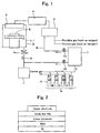
- Fig. 1 is a schematic diagram showing an example of the structure of a thin film-forming apparatus according to the present invention.
- the CVD thin film-forming apparatus as shown in Fig. 1 comprises a vacuum exhaust system 1, a reaction chamber 2 connected to the vacuum exhaust system 1 through a pressure-control valve 1a, a shower plate 3 arranged at the upper portion of the reaction chamber 2, a gas activating means 4, a gas-mixing unit 5, an evaporator 7 serving as a vaporization system connected to the gas-mixing unit 5 through a raw gas-pipe line 6.
- a raw material which is evaporated in the evaporator 7 is mixed with a reaction gas and a dilution gas in the gas-mixing unit 5, and then a gas mixture thus obtained is introduced into the shower plate 3.
- this gas mixture is introduced into the shower plate directly.
- the gas activating means is arranged between the shower plate 3 and the gas mixing unit 5, and the gas mixture is introduced into the shower plate through the gas activating means.
- This gas activating means may be, for example, a gas pipe line.
- the pipe line 6 is provided with a valve V1 positioned between the evaporator 7 and the gas-mixing unit 5, while a pipe line 8 is equipped with a valve V2 positioned between the evaporator 7 and the vacuum exhaust system 1 so that the evaporator 7, the gas-mixing unit 5 and the vacuum exhaust system 1 can be isolated from one another.
- each of the structural elements for these evaporator 7, gas-mixing unit 5 and vacuum exhaust system 1 differ from one another in the maintenance cycle and therefore, when they are opened to the air, substances such as moisture which may adversely affect the films formed may be adhered to these elements. For this reason, these members are isolated from one another to prevent the adhesion of any such harmful substance. More specifically, the apparatus of the present invention is so designed that when one structural element is opened to the air to perform the maintenance thereof, the other two elements can be maintained at a vacuum without opening them to the air.
- the foregoing gas activating means 4 is equipped with a heating means such as a heater, ultraviolet rays heating unit, micro wave heating unit, or plasma heating unit. These heating means serve to maintain the gas activating means at the temperature without causing any liquefaction, deposition, or film-formation of the raw gas.
- a heating means such as a heater, ultraviolet rays heating unit, micro wave heating unit, or plasma heating unit.
- a temperature of the gas activating means is set at a temperature from room temperature to 400°C, preferably 165 ⁇ 360°C, more preferably 165 ⁇ 250°C to perform the film-forming process, depending on the raw materials to be used. If set temperature is too low, deposition of the raw gas is caused, and this would result in the generation of particles. If the set temperature is too high, the raw material is too decomposed to thus generate of particles.
- the gas mixture after passing through the gas activating means is preferably introduced into the shower plate directly.
- a stage 2-1 for mounting a substrate S to be covered with a desired film which is provided with a means for heating the substrate and a gas mixture for film forming is supplied onto the surface of the substrate heated through the shower plate 3.
- the excess gas mixture which is not used for the reaction with the substrate S, the by-product gas generated through the reaction of the gas mixture with the substrate and a part of the reaction product gas are discharged by the action of the exhaust system 1.
- the shower plate 3 is moderately heated to thus maintain the same to a temperature which never causes any liquefaction, deposition and/or film-formation of the introduced gas.
- the shower plate 3 positioned at the upper portion of the reaction chamber 2 may be equipped with a particle capture or trap serving as a filter for trapping particles present in the gas mixture.
- This particle capture may be arranged at a position immediately before the shower hole of the shower plate and it is appropriately and desirably controlled to a temperature which can ensure the prevention of any adhesion and/or capture of the vaporized specific raw element required for the reaction.
- the apparatus can easily cope with a variety of pressure conditions for forming a film due to the presence of the pressure-control valve 1a arranged between the foregoing exhaust system 1 and the reaction chamber 2.
- the gas-mixing unit 5 is connected to the evaporator 7 through the pipe line equipped with the valve V1 and likewise simultaneously connected to two gas sources (for instance, an oxidation gas source such as an oxygen source; a dilution gas source such as an inert gas (such as nitrogen gas) source) through a valve, a heat-exchanger and a mass controller (not shown).
- gas sources for instance, an oxidation gas source such as an oxygen source; a dilution gas source such as an inert gas (such as nitrogen gas) source
- the gas mixture prepared by uniformly admixing desired gaseous components in the gas-mixing unit 5 passes through the gas activating means 4, is then introduced into the reaction chamber 2 through the shower plate 3 and supplied onto the surface of the subject on which a film is formed and which is mounted on the stage 2-1 without forming any laminar flow in the reaction chamber.
- the oxidation gas supplied from the oxidation gas source and heated to an appropriate temperature, the raw gas generated in the evaporator 7 and supplied through the pipe line 6 maintained at a temperature which never causes any liquefaction, decomposition and/or film-formation of the gas, and the inert gas are introduced into and admixed in the gas-mixing unit 5 to thus form a gas mixture (a uniform mixture of oxidation gas and raw gas).
- the raw gas is a gas mixture containing one or a plurality of raw gases.
- the gas mixture thus prepared is fed to the reaction chamber through the gas activating means 4.
- These gas activating means 4 and pipe line 6 may be connected to one another through a VCR joint and a VCR gasket for a part of the joint of the pipe line is not a simple ring, but may be provided with a VCR type particle capture at the hole thereof.
- the joint provided with such a VCR type particle capture is desirably set and maintained at a temperature higher than that accompanied by the liquefaction, decomposition and/or film-formation of the raw gas so as not to cause any adhesion and/or capture of the specific vaporized raw element required for the reaction.
- the gas activating means 4 positioned between the gas-mixing unit 5 and the shower plate 3 may be provided with a valve for switching the gas mixture on the secondary side of the gas-mixing unit 5.
- the valve is connected to the reaction chamber 2 at the downstream side thereof. The valve is opened when a film is formed and it is closed after the completion of the film-forming step.
- the evaporator 7 is connected to a raw material-supply zone 7a and an evaporation zone (not shown).
- the evaporator is so designed that it pressurizes and transports liquid raw materials A, B and C prepared by dissolving liquid or solid raw materials in organic solvents through the use of a pressurized gas (for instance, an inert gas such as He gas), the flow rates of these liquid raw materials fed under pressure are controlled by corresponding flow rate controllers and the liquid raw materials are thus transported to the evaporation zone by the action of a carrier gas.
- a pressurized gas for instance, an inert gas such as He gas
- the evaporator is likewise so designed that the liquid raw materials whose flow rates are controlled can efficiently be evaporated in the evaporation zone and the resulting raw gas can be fed to the gas-mixing unit 5.
- the evaporation zone permits the mixing and evaporation of a single liquid raw material or a plurality of liquid raw materials.
- the evaporation of a liquid raw material is preferably carried out not only by evaporating droplets of the liquid raw material, but also by injecting a gas stream to these droplets or applying physical vibrations or ultrasonics to the droplets, converting the liquid particles thus formed into finer particles by passing through a nozzle positioned on the wall of the evaporation zone prior to the introduction thereof into the evaporation zone and then evaporating these liquid particles to thus improve the evaporation efficiency.
- evaporation members produced from a material excellent in the heat conduction such as Al may be disposed within the evaporation zone so that liquid particles or droplets can quite efficiently be evaporated in place and to reduce liquid particle-evaporation loads of a variety of particle captures.
- a particle capture may be arranged in the evaporation zone such that any particle originated from the residue generated when the liquid raw material is evaporated is never discharged from the evaporation zone and that the droplets entering into the zone in a small amount can be evaporated without external evacuation of the same by the action of a vacuum.
- the evaporation members and the particle capture be maintained at an appropriate temperature as an evaporation condition so as to certainly evaporate droplets and fine liquid particles which come in contact with these components and to prevent the adhesion of any evaporated specific raw element required for the reaction to these components and/or the capture of such element by these components.
- the evaporator 7 may likewise be so designed that it comprises a solvent D for the dissolution of the raw material and that the resulting solution is introduced into the evaporation zone while controlling the flow rate thereof by a flow rate controller to thus evaporate the solution and to thus prepare a solvent gas.
- the solvent gas may be used for the cleaning of the interior of the apparatus.
- the apparatus for preparing the thin film of the present invention preferably comprises a reaction chamber 2 having a cylindrical shape and the reaction chamber is provided therein with a substrate stage 2-1 likewise having a cylindrical shape on which a substrate such as a silicon wafer is mounted.
- a heating means is incorporated into the stage 2-1 to heat the substrate.
- the reaction chamber 2 may be provided with a means for freely ascending and descending the stage 2-1 between the film-forming position within the reaction chamber and the substrate-conveying position at a lower position in the chamber.
- the apparatus is likewise so designed that a shower plate 3 is disposed at the central portion on the upper side of the reaction chamber 2 so that it is opposed to the substrate stage 2-1 and that the film-forming gas from which the particles are removed can be injected towards the center of the substrate through the shower plate 3.
- the pipe line for the oxidation gas is provided with a heat-exchanger as a means for controlling the gas temperature and a heating means such as a heater is fitted to the outer wall of the reaction chamber 2 and/or the substrate stage 2-1 to thus prevent the separation of any raw gas.
- the method for the preparation of the present invention using the apparatus for preparing the thin film shown in Fig.1 would permit the formation of a PZT ferroelectric film according to the CVD technique using, as a raw material, an organometal compound, for instance, a liquid raw material such as Pb(DPM) 2 , Zr(DMHD) 4 or Ti(i-PrO) 2 (DPM) 2 ; the formation of CVD thin film of PZT; and the formation of a BST ferroelectric film according to the CVD technique using a liquid raw material such as Ba(DPM) 2 , Sr(DPM) 2 , or Ti(i-PrO) 2 (DPM) 2 ; as well as the formation of a thin film mainly used as a metallic wire distribution of, for instance, Cu and Al, a thin film mainly used as a barrier of, for instance, TiN, TaN, ZrN, VN, NbN and Al 2 O 3 , or a thin film of a dielectric material such as S
- the raw gas is one obtained by heating and vaporizing, a raw material which is a gas, liquid or solid in ordinary temperature.
- the raw gas may be one obtained by vaporizing a liquid raw material or a solution of a solid raw material in a solvent.
- the gas mixture also can be introduced into the reaction chamber through a pipe line which is equipped with the foregoing heating means and serves as the gas activating means 4 arranged between the gas-mixing unit 5 and the shower plate 3 shown in Fig. 1 .
- the pipe line permits the desired activation of the gas if a surface area of inner wall thereof is within the range of 4.8 ⁇ 10 -3 m 2 to 1.28 ⁇ 10 -1 m 2 .
- Such a structure of the pipe line would permit the activation of the raw gas and the realization of excellent epitaxial growth.
- the decomposition step of the raw material to be introduced into the reaction chamber can be optimized to thus obtain the desired metal atom-containing molecules.
- the film is formed efficiently and the film properties (such as leak electric current density, polarization-inversion charge density and polarization-saturation voltage) are improved.
- the surface area of inner wall of the pipe line is less than 4.8 ⁇ 10 -3 m 2 , the gas of organic material is insufficiently decomposed and accordingly, the resulting film has a large amount of oxygen loss therein.
- the surface area of inner wall thereof is too large, the vapor phase decomposition of the raw gas is caused, and a problem arises such that the film-forming rate decreased due to deposition on the inner wall of the pipe line, the consumption of the raw material increases, and the production cost becomes high due to increases in the surface area of the apparatus and the number of parts whose temperature should be controlled.
- the preferred and acceptable upper limit of the internal wall surface area is about 1.28 ⁇ 10 -1 m 2 .
- the inner diameter of the pipe line is one which is used in general (almost 105 ⁇ 20.5mm) and a length of the pipe line is about 150 ⁇ 1625mm, it is possible to accomplish the some effect.
- the amount of the atom to be contained in the initial layer is preferably heightened to a level higher than in the substrate in which the atom hardly diffuses.
- a ferroelectric film free of any foreign phase and capable of saturating the spontaneous polarization at a low voltage could be prepared by increasing the rate of Pb in the seed layer (initial layer).
- Fig.15 ⁇ 22 which will hereinafter be explained, make it clear.
- the present invention having the foregoing construction permits the improvement of any oxygen defect.
- the epitaxial growth of a film can be promoted and a ferroelectric thin film having a regular orientation and a low leak electric current and whose spontaneous polarization is saturated at a low voltage can be prepared by forming a seed layer ( an initial layer) during the nucleation in a lower rate of oxidation gas flow rate and successively increasing the rate of oxidation gas flow rate to grow a film at the oxidation gas rate that is higher than that used in the initial layer
- THF tetrahydrofuran
- the raw gas thus obtained through evaporation was transported to the gas-mixing unit 5 through the pipe line 6, the raw gas was admixed with oxygen (flow rate of 3500 sccm) as an oxidation gas and nitrogen (300 sccm) as a dilution gas, the resulting mixed gas was then transported to the shower plate 3 through the gas activating means 4, and the gas mixture was then fed to the surface of a substrate S mounted in the reaction chamber 2 and heated to a temperature of 620°C to deposit a PZT thin film and to thus form a desired thin film.
- oxygen flow rate of 3500 sccm
- nitrogen 300 sccm
- the pressure in the reaction chamber was adjusted to about 667 Pa using a pressure control valve 1a.
- the pressure in the reaction chamber was adjusted to about 133.3Pa ⁇ 3999Pa so that the pressure in the gas activating means 4 is a little higher than that of the reaction chamber.
- the temperature of the gas activating means needs to control to a level which never causes any deposition of the raw material. In the case of Pb(thd) 2 complex used in this Example, the temperature adjusted to the level ranging from about 210 to 250°C.
- a film was formed while the temperature of the substrate S was maintained at 620°C by heating the substrate stage 2-1, but the film-forming process was in general carried out at a temperature ranging from about 500 to 650°C.
- the substrate used above was one comprising a Si wafer on which a SiO 2 film had been formed through thermal oxidation and a lower electrode had likewise been formed on the SiO 2 film surface in the form of a film.
- the lower electrode may be formed from a material such as Pt, Ir, Rh, Ru, MgO, SrTiO 3 , IrO 2 , RuO 2 , SrRuO 3 and LaNiO 3 , which are oriented in a certain plane direction, but Ir/SiO 2 /Si, Pt/Ti/SiO 2 /Si and SRO/Pt/Ti/SiO 2 /Si were used in this Example.
- a PZT ferroelectric oxide thin film was formed on the lower electrode according to the foregoing procedures in a thickness of 100 nm, a Pt film as an upper electrode was formed on the oxide thin film by the sputtering through a mask (a diameter of 0.3 mm) for the evaluation of electric characteristics of the resulting PZT ferroelectric oxide thin film.
- the resulting structure was used in the following Examples as a sample for the evaluation of a variety of characteristic properties.
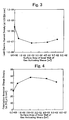
- Fig. 3 is a graph showing the dependency of the leak electric current density (A/cm 2 ) of the PZT thin film, observed when a voltage of 1.5 V is applied thereto, on the surface area (m 2 ) of inner wall of the gas activating means.
- the rate of oxygen gas flowing through the reaction chamber 2 was set at 91% on the basis of the total gas supplied.
- the substrate used was an Ir(111)-oriented film.
- the leak electric current density was found to be 2.5E-6A/cm 2 in the case of not using the gas activating means (a surface area of inner wall is 0m 2 ) and 2.0E-7 A/cm 2 for a surface area of inner wall of the gas activating means of 4.8E-3 m 2 .
- the leak current density was reduced and it reached a minimum value of 7.5E-8A/cm 2 at the surface area of inner wall of 2.1E-2 m 2 .
- the surface area of inner wall was further increased, the leak current density was increased and it was found to be 1.7E-7A/cm 2 for a surface area of inner wall of 5.2E-2m 2 .
- Fig. 4 is a graph showing the dependency of the polarization-inversion charge density of the PZT thin film, observed when a voltage of 2.0 V is applied thereto, on the surface area of inner wall of the gas activating means.
- the polarization-inversion charge density of the film was found to be 28 ⁇ C/cm 2 without using the gas activating means and 39 ⁇ C/cm 2 at a surface area of inner wall of 4.8E-3 m 2 .
- the polarization-inversion charge density was reduced and it was found to be 40 ⁇ C/cm 2 at surface area of inner wall of 5.2E-2m 2
- Fig. 5 is a graph showing the dependency of the polarization-saturation voltage of the PZT thin film on the surface area of inner wall of the gas activating means.
- the polarization-saturation voltage of the film was found to be 2.2 V without using the gas activating means and 1.90 V at the surface area of inner wall of 4.8E-3 m 2 . However, it was reduced as the surface area of inner wall was increased and the voltage reached a minimum value of 1.7 V at the surface area of inner wall of 2.1E-2 m 2 . On the other hand, if the surface area of inner wall is further increased, the polarization-saturation voltage of the film was increased and it was found to be 1.83 V at the surface area of inner wall of 5.2E-2m 2 .
- the inventors of this invention have determined the decomposition steps of metal atom-containing molecules and have found that after mixing the oxidation gas and the raw gas obtained through evaporation, the gas activating means which control the state of gas phase decomposition are arranged, and that the metal atom-containing molecules obtained at the steps which permit the preparation of films having good characteristic properties must be introduced into the reaction chamber through the shower plate in order to efficiently form a film and to improve the characteristic properties of the resulting film.
- Fig. 6 is a graph showing the dependency of the leak electric current density of the PZT thin film, observed when a voltage of 1.5 V is applied thereto, on the flow rate of oxygen in the gas mixture on the basis of the total gases introduced.
- the rate of oxygen flow rate is changed within the range of 0.5 - 95%
- a surface area of inner wall of the gas activating means was set at 2.1E-2 m 2 and the substrate used was an Ir(111)-oriented film.
- the leak current density was found to be 1E-1 and it was gradually reduced as the oxygen flow rate was increased.
- Fig. 7 the X-ray diffraction (XRD) pattern determined for the PZT thin film clearly indicate that the (111)-orientation intensity observed at an oxygen flow rate of 80% (the pattern b in Fig. 7 ) was significantly reduced as compared with that observed at an oxygen flow rate of 5% (the pattern a in Fig. 7 ).
- Pb / (Zr + Ti) equal to 1.15.
- Fig. 8 is a graph showing the dependency of the rate of the PZT(111) intensity on the basis of the total orientation intensity of the PZT thin film as determined by the XRD while changing the rate of oxygen flow rate (0.5 to 95%), in the gas mixture.
- the XRD(111) intensity was reduced as the oxygen flow rate was increased. From the foregoing, it would be recognized that the reduction of the leak electric current density and the epitaxial growth of the film are in a trade-off relation.
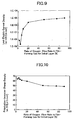
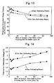
- Fig. 9 is a graph showing the dependency of the leak electric current density of the PZT thin film, observed when a voltage of 1.5 V is applied thereto, on the initial layer-oxygen flow rate in the preparation of the initial layer.
- the thicknesses of initial and second layers were set at 5 nm and 100 nm, respectively.
- the leak current density was found to be a minimum of 2E-9 for an initial layer-oxygen flow rate of 5% and it was increased as the initial layer-oxygen flow rate was increased. It is recognized from the Fig. 9 that leak electric current density is sufficiently low even when the rate of oxygen flow rate for forming the initial layer is 0.5%, the desired value of the leak electric current density is obtained if the rate of oxygen flow rate is up to less than about 60%, preferably up to about 20%.
- Fig. 10 is a graph showing the dependency of the polarization-inversion charge density of the PZT thin film, observed when a voltage of 2.0 V is applied thereto, on the initial layer-oxygen flow rate in the preparation of the initial layer.
- the polarization-inversion charge density reached a maximum value of 66 ⁇ C/cm 2 at an initial layer-oxygen flow rate of 5% and thereafter, it was reduced as the initial layer-oxygen flow rate was increased. It is recognized from the Fig.10 that the polarization-inversion charge density is sufficiently high even when the rate of oxygen flow rate for forming the initial layer is 0.5%, the desired value of the polarization-inversion charge density is obtained if the rate of oxygen flow rate is up to less than about 60%, preferably up to about 20%.
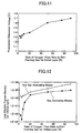
- Fig. 11 is a graph showing the dependency of the polarization-saturation voltage on the initial layer-oxygen flow rate in the preparation of the initial layer.
- the polarization-saturation voltage reached its minimum value of 1.29 V at an initial layer-oxygen flow rate of 5% and thereafter, it was reduced as the initial layer-oxygen flow rate was increased. It is recognized from the Fig. 11 that the polarization-saturation voltage is sufficiently low even when the rate of oxygen flow rate for forming the initial layer is 0.5%, the desired value of polarization-saturation voltage is obtained if the rate of oxygen flow rate is up to less than about 60%, preferably up to about 20%.
- Figs. 12 , 13 and 14 are graphs showing the dependency of the leak electric current density of the PZT thin film, observed when a voltage of 1.5 V is applied thereto, the polarization-inversion charge density of the PZT thin film observed when a voltage of 2.0 V is applied thereto and the polarization-saturation voltage, on the initial layer-oxygen flow rate in the preparation of the initial layer, which are observed when the apparatus is equipped with the gas activating means (the line a in these figures; the surface area of its inner wall: 2.1E-2m 2 )and not equipped with the gas activating means.
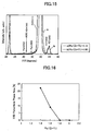
- the dependency of characteristic properties of the PZT thin film formed on a Pt substrate on the Pb/(Zr + Ti) composition in the initial layer will be detailed in this Example.
- the surface area of inner wall of the gas activating means arranged between the gas-mixing unit and the shower plate was set at 2.08E-02m 2
- the substrate used was a Pt/Ti/SiO 2 /Si substrate.
- Fig. 15 is a diagram showing the X-ray diffraction (XRD) pattern observed for the PZT thin film.
- there was observed only the PZT perovskite monophase for the film of Pb / (Zr + Ti) 1.80 (the curve b in Fig. 15).
- an initial layer as a seed layer and a second layer film were formed in succession to thus improve the properties of the resulting thin film.
- the initial layer for forming initial nuclei was formed at an oxygen flow rate of 5% in a thickness of 5 nm, while changing the ratio: Pb/(Zr + Ti).
- the second layer was formed at an oxygen flow rate of 91 % in a thickness of 100 nm.
- Fig. 17 is a graph showing the dependency of the rate of the pyrochlore phase in the XRD intensity on the composition of Pb/(Zr + Ti) present in the initial layer. From the data shown in Fig. 17 , it would be estimated that the PZT monophase is formed at a ratio: Pb/(Zr + Ti) of not less than 1.69.
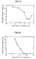
- Fig. 18 is a graph showing the dependency of the polarization-inversion charge density on the composition of Pb/(Zr + Ti) present in the initial layer.
- the polarization-inversion charge density increases as the ratio: Pb/(Zr + Ti) in the composition of the film increases and the charge density reached a maximum value of 52 ⁇ C/cm 2 at a ratio: Pb/(Zr + Ti) of 1.75.
- the polarization-inversion charge density was slowly reduced at higher ratios.
- Fig. 19 is a graph showing the dependency of the polarization-saturation voltage on the composition of Pb/(Zr + Ti) present in the initial layer.
- the PZT monophase can be obtained at a ratio: Pb/(Zr + Ti) ranging from 1.69 to 1.82 and that PbO paraelectric layers were mixed therein at a ratio: Pb/(Zr + Ti) of 1.93.
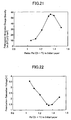
- Fig. 20 is a graph showing the dependency of the rate of the pyrochlore phase in the XRD intensity on the composition of the initial layer or the ratio: Pb/(Zr + Ti).
- an internal surface area of the gas activating means was set at 2.08E-2m 2 and the substrate used was an SRO/Pt/Ti/SiO 2 /Si substrate.
- An initial layer film was prepared using an oxygen flow rate of 91% and a second layer film was prepared using an oxygen flow rate of 91%.
- the rate of the pyrochlore phase is reduced as the ratio: Pb/(Zr + Ti) increases and it was found to be zero at a ratio: Pb/(Zr + Ti) of not less than 1.31.
- Fig. 21 is a graph showing the dependency of the polarization-inversion charge density on the composition of the initial layer or the ratio: Pb/(Zr + Ti) in the initial layer.
- the charge density increases as the ratio: Pb/(Zr + Ti) increases and it reached a maximum value of 56 ⁇ C/cm 2 at a ratio: Pb/(Zr + Ti) of 1.31.
- Fig. 22 is a graph showing the dependency of the polarization-saturation voltage on the composition of the initial layer or the ratio: Pb/(Zr + Ti) in the initial layer.
- the polarization-saturation voltage is reduced as the ratio: Pb/(Zr + Ti) increases and it showed a minimum value of 1.41 V at a ratio: Pb/(Zr + Ti) of 1.31.
- the object of the present invention can be accomplished by a continued application of film-formation which is performed using the film rich in Pb as the initial layer and the film containing reduced Pb as the second layer.
- PZT thin films were prepared according to the foregoing Examples, provided that pipe lines each having a different inner diameter were used as the gas activating means, and the properties of the film thus obtained were compared.
- Table.1 shows the relation between an surface area of inner wall of each pipe line and a length of each pipe line when the internal diameter of the pipe line is 10.2mm and 25mm.
- Fig.23 is a graph showing the dependency of the leak current density (A/cm 2 ) of the resulting PZT thin film on the surface areas of inner wall of the pipe lines used as the gas activating means when a voltage of 1.5V is applied thereto. It is clearly recognized from this figure that, if the pipe lines are identical in the surface area of inner wall, the leak electric current density of the thin films is almost identical with each other even if the pipe lines have the different inner diameter.
- Fig 24 is a graph showing the dependency of a polarization-inversion charge density when a voltage of 2.0V was applied to the PZT thin film obtained according to the foregoing method
- Fig. 25 is a graph showing the dependency of the polarization-saturation voltage on surface area of inner wall of a pipe line used the gas activating means. It can be clearly recognized from these figures that, if the pipe lines are identical in the surface area of inner wall, the polarization-inversion charge density and the polarization-saturation voltage of the thin films show the almost same tendency as in the case of the leak electric current density, even if the pipe lines have the different inner diameter.
- the epitaxial growth of a film is promoted and a ferroelectric thin film having regular orientation and a low leak current density and whose spontaneous polarization is saturated at a low voltage can be prepared by using the oxidation gas of rate of the flow rate such that prescribed the partial pressure of the oxygen is obtained.
- metal atom-containing molecules obtained in the decomposition step of the raw gas which permits the preparation of films having good characteristic properties are introduced into the reaction chamber to use the molecules for the preparation of the ferroelectric thin film.
- a method for the preparation of a ferroelectric thin film having excellent characteristic properties are provided.
- an apparatus for preparing the thin film having the improved oxide defect are quite useful in the fields of semiconductor element-production.
Claims (4)
- Verfahren zur Herstellung eines Oxiddünnfilms auf einem Substrat, enthaltend als Schritte das Vermischen eines durch Verdampfen eines Rohmaterials für den Oxiddünnfilm erhaltenen Rohgases, eines Trägergases und eines Oxidationsgases in einer Gasmischeinheit und Zuführen des resultierenden Gasgemischs durch eine Brauseplatte auf ein in einer Reaktionskammer als chemischer Gasphasenabscheidungsvorrichtung angeordnetes, erhitztes Substrat, um das Gasgemisch so gegenseitig zum Reagieren zu bringen, das Zuführen des Gasgemischs zur Reaktionskammer durch ein zwischen der Gasmischeinheit und der Brauseplatte angeordnetes Gas-Aktivierungsmittel, das eine Rohrleitung umfasst, deren innere Wandoberfläche 4,8 x 10⁻³ m2 bis 1,28 x 10⁻¹ m2 beträgt und die auf einer solchen Temperatur gehalten wird, dass das Rohgas beim Einleiten des Rohgases in die Brauseplatte in der Gasphase in metallatomhaltige Moleküle aufgespaltet wird, die einen Film mit den gewünschten Eigenschaften bilden können; wobei der Anteil der Durchflussmenge des Oxidationsgases bezogen auf das Gasgemisch nicht weniger als 60 % beträgt; und wobei der Oxiddünnfilm ein Oxid eines aus der Gruppe bestehend aus SiO2, TiO2, Al2O3, Ta2O5, MgO, ZrO2, HfO2, (Ba, Sr)TiO2 und SrTiO3 ausgewählten paraelektrischen dielektrischen Materials; oder ein Oxid eines aus der Gruppe bestehend aus Pb(Zr, Ti)O3, SrBi2Ta2O9 und Bi4Ti3O12 ausgewählten ferroelektrischen Materials ist.
- Verfahren zur Herstellung eines Oxiddünnfilms nach Anspruch 1, wobei das Oxidationsgas ein Mitglied aus der Gruppe bestehend aus Sauerstoff, Ozon, N2O und NO2 ist.
- Verfahren zur Herstellung eines Oxiddünnfilms nach einem der Ansprüche 1 bis 2, wobei das verwendete Trägergas ein aus der Gruppe bestehend aus Stickstoff, Helium, Argon, Neon und Krypton ausgewähltes Inertgas ist.
- Verfahren zur Herstellung eines Oxiddünnfilms nach einem der Ansprüche 1 bis 3, wobei das Substrat ein aus einem aus der Gruppe bestehend aus Pt, Ir, Rh, Ru, MgO, SrTiO3, IrO2, RuO2, SrRuO3 und LaNiO3 ausgewählten Material hergestelltes Substrat ist.
Applications Claiming Priority (2)
| Application Number | Priority Date | Filing Date | Title |
|---|---|---|---|
| JP2003300014 | 2003-08-25 | ||
| PCT/JP2004/012180 WO2005020311A1 (ja) | 2003-08-25 | 2004-08-25 | 酸化物薄膜製造方法及びその製造装置 |
Publications (3)
| Publication Number | Publication Date |
|---|---|
| EP1662556A1 EP1662556A1 (de) | 2006-05-31 |
| EP1662556A4 EP1662556A4 (de) | 2012-05-09 |
| EP1662556B1 true EP1662556B1 (de) | 2013-11-06 |
Family
ID=34213796
Family Applications (1)
| Application Number | Title | Priority Date | Filing Date |
|---|---|---|---|
| EP04772141.0A Active EP1662556B1 (de) | 2003-08-25 | 2004-08-25 | Prozess zur herstellung eines oxid-dünnfilms |
Country Status (7)
| Country | Link |
|---|---|
| US (1) | US20070054472A1 (de) |
| EP (1) | EP1662556B1 (de) |
| JP (1) | JP4628954B2 (de) |
| KR (2) | KR101246499B1 (de) |
| CN (1) | CN100435294C (de) |
| TW (1) | TW200511404A (de) |
| WO (1) | WO2005020311A1 (de) |
Families Citing this family (7)
| Publication number | Priority date | Publication date | Assignee | Title |
|---|---|---|---|---|
| JP2008053683A (ja) * | 2006-07-27 | 2008-03-06 | Matsushita Electric Ind Co Ltd | 絶縁膜形成方法、半導体装置、および基板処理装置 |
| KR20090042285A (ko) * | 2006-08-02 | 2009-04-29 | 가부시키가이샤 아루박 | 막 형성방법 및 막 형성장치 |
| JP2010080813A (ja) * | 2008-09-29 | 2010-04-08 | Fujifilm Corp | 圧電体膜とその製造方法、圧電素子、及び液体吐出装置 |
| TWI452946B (zh) * | 2009-12-29 | 2014-09-11 | Univ Nat Yunlin Sci & Tech | Plasma reaction device |
| JP2014150191A (ja) * | 2013-02-01 | 2014-08-21 | Ulvac Japan Ltd | Pzt膜の製造方法及び成膜装置 |
| CN106367732B (zh) * | 2016-09-22 | 2018-11-06 | 四川大学 | 一种中温金属有机化学气相沉积TiO2-Al2O3复合涂层装置及涂覆方法 |
| CN110586180B (zh) * | 2019-09-20 | 2022-06-14 | 湖南师范大学 | 一种具有可见光催化n2o参与选择性氧化的钌杂化十聚钨酸季铵盐的制备方法 |
Family Cites Families (15)
| Publication number | Priority date | Publication date | Assignee | Title |
|---|---|---|---|---|
| JPH086181B2 (ja) * | 1992-11-30 | 1996-01-24 | 日本電気株式会社 | 化学気相成長法および化学気相成長装置 |
| KR960015375B1 (ko) * | 1994-06-08 | 1996-11-11 | 현대전자산업 주식회사 | 강유전체 박막 제조장치 및 그를 사용한 강유전체 박막 제조방법 |
| JPH08268797A (ja) * | 1995-03-30 | 1996-10-15 | Hitachi Ltd | 化学気相反応堆積装置 |
| US5989998A (en) * | 1996-08-29 | 1999-11-23 | Matsushita Electric Industrial Co., Ltd. | Method of forming interlayer insulating film |
| JPH1131650A (ja) * | 1997-07-14 | 1999-02-02 | Kokusai Electric Co Ltd | 反射防止膜、被処理基板、被処理基板の製造方法、微細パターンの製造方法、および半導体装置の製造方法 |
| US6080499A (en) * | 1997-07-18 | 2000-06-27 | Ramtron International Corporation | Multi-layer approach for optimizing ferroelectric film performance |
| JP3109485B2 (ja) * | 1998-08-03 | 2000-11-13 | 日本電気株式会社 | 金属酸化物誘電体膜の気相成長方法 |
| EP1143501A4 (de) * | 1998-12-16 | 2005-02-02 | Tokyo Electron Ltd | Verfahren zur herstellung einer dünnschicht |
| US6495878B1 (en) * | 1999-08-02 | 2002-12-17 | Symetrix Corporation | Interlayer oxide containing thin films for high dielectric constant application |
| US6811651B2 (en) * | 2001-06-22 | 2004-11-02 | Tokyo Electron Limited | Gas temperature control for a plasma process |
| US20030012875A1 (en) * | 2001-07-10 | 2003-01-16 | Shreyas Kher | CVD BST film composition and property control with thickness below 200 A for DRAM capacitor application with size at 0.1mum or below |
| JP2003086586A (ja) * | 2001-09-13 | 2003-03-20 | Murata Mfg Co Ltd | 配向性強誘電体薄膜素子及びその製造方法 |
| US6713127B2 (en) * | 2001-12-28 | 2004-03-30 | Applied Materials, Inc. | Methods for silicon oxide and oxynitride deposition using single wafer low pressure CVD |
| JP3971645B2 (ja) * | 2002-04-30 | 2007-09-05 | 富士通株式会社 | 半導体装置の製造方法 |
| US6884464B2 (en) * | 2002-11-04 | 2005-04-26 | Applied Materials, Inc. | Methods for forming silicon comprising films using hexachlorodisilane in a single-wafer deposion chamber |
-
2004
- 2004-08-25 WO PCT/JP2004/012180 patent/WO2005020311A1/ja active Application Filing
- 2004-08-25 KR KR1020117021973A patent/KR101246499B1/ko active IP Right Grant
- 2004-08-25 KR KR1020067003747A patent/KR101179098B1/ko active IP Right Grant
- 2004-08-25 US US10/569,470 patent/US20070054472A1/en not_active Abandoned
- 2004-08-25 CN CNB2004800243173A patent/CN100435294C/zh active Active
- 2004-08-25 JP JP2005513346A patent/JP4628954B2/ja active Active
- 2004-08-25 EP EP04772141.0A patent/EP1662556B1/de active Active
- 2004-08-26 TW TW093125554A patent/TW200511404A/zh unknown
Also Published As
| Publication number | Publication date |
|---|---|
| TWI363377B (de) | 2012-05-01 |
| US20070054472A1 (en) | 2007-03-08 |
| WO2005020311A1 (ja) | 2005-03-03 |
| KR101246499B1 (ko) | 2013-03-25 |
| KR20060118418A (ko) | 2006-11-23 |
| JPWO2005020311A1 (ja) | 2007-11-01 |
| JP4628954B2 (ja) | 2011-02-09 |
| EP1662556A1 (de) | 2006-05-31 |
| CN1842901A (zh) | 2006-10-04 |
| KR101179098B1 (ko) | 2012-09-03 |
| EP1662556A4 (de) | 2012-05-09 |
| CN100435294C (zh) | 2008-11-19 |
| KR20110116065A (ko) | 2011-10-24 |
| TW200511404A (en) | 2005-03-16 |
Similar Documents
| Publication | Publication Date | Title |
|---|---|---|
| JP3462852B2 (ja) | 化学気相成長法によって薄膜を製造する方法と装置 | |
| JP5719849B2 (ja) | 薄膜製造方法 | |
| US6110531A (en) | Method and apparatus for preparing integrated circuit thin films by chemical vapor deposition | |
| KR100468847B1 (ko) | 알콜을 이용한 금속산화물 박막의 화학기상증착법 | |
| US6787181B2 (en) | Chemical vapor deposition method of making layered superlattice materials using trimethylbismuth | |
| EP1662556B1 (de) | Prozess zur herstellung eines oxid-dünnfilms | |
| KR100945096B1 (ko) | 용량 소자의 제조 방법 | |
| JPH08176826A (ja) | Cvd法による薄膜の堆積装置及び堆積方法並びに該堆積装置又は該堆積方法で用いられるcvd原料及び液体原料容器 | |
| EP2053643A1 (de) | Filmbildungsverfahren und filmbildungsvorrichtung | |
| KR970018599A (ko) | 산화 비스무스의 생성방법, 산화물막의 형성방법, 및 반도체 소자의 캐패시터 구조의 제작방법 | |
| JPH09246214A (ja) | 薄膜形成方法、半導体装置及びその製造方法 | |
| US6863726B2 (en) | Vapor phase growth method of oxide dielectric film | |
| JP2007506271A (ja) | 液状又は溶液の原料を用いマルチチャンネル装置を介して不連続に射ち込み、単元又は多元の層及びスタック層を堆積する方法及び装置 | |
| JP4205565B2 (ja) | 薄膜製造方法 | |
| JP4243171B2 (ja) | 金属酸化物薄膜の形成方法 | |
| JP3886921B2 (ja) | 化学気相堆積方法 | |
| EP1734151A1 (de) | Verfahren und Vorrichtung zur metalorganischen, chemischen Dampfabscheidung (MOCVD) und Ausglühen dünner Bleigermanit- (PGO-) Filmen | |
| JP4473540B2 (ja) | 薄膜製造方法及びパーティクル数の評価方法 | |
| KR100648142B1 (ko) | 유전체막의 제조방법 | |
| JPH07252658A (ja) | 誘電体薄膜の形成方法およびその装置 | |
| JPH09110429A (ja) | ビスマス層状強誘電体薄膜の製造方法 |
Legal Events
| Date | Code | Title | Description |
|---|---|---|---|
| PUAI | Public reference made under article 153(3) epc to a published international application that has entered the european phase |
Free format text: ORIGINAL CODE: 0009012 |
|
| 17P | Request for examination filed |
Effective date: 20060303 |
|
| AK | Designated contracting states |
Kind code of ref document: A1 Designated state(s): DE IT |
|
| DAX | Request for extension of the european patent (deleted) | ||
| RBV | Designated contracting states (corrected) |
Designated state(s): DE IT |
|
| A4 | Supplementary search report drawn up and despatched |
Effective date: 20120410 |
|
| RIC1 | Information provided on ipc code assigned before grant |
Ipc: C23C 16/448 20060101ALI20120402BHEP Ipc: H01L 21/316 20060101AFI20120402BHEP Ipc: C23C 16/40 20060101ALI20120402BHEP Ipc: C23C 16/452 20060101ALI20120402BHEP |
|
| 17Q | First examination report despatched |
Effective date: 20120919 |
|
| GRAP | Despatch of communication of intention to grant a patent |
Free format text: ORIGINAL CODE: EPIDOSNIGR1 |
|
| INTG | Intention to grant announced |
Effective date: 20130528 |
|
| GRAS | Grant fee paid |
Free format text: ORIGINAL CODE: EPIDOSNIGR3 |
|
| GRAA | (expected) grant |
Free format text: ORIGINAL CODE: 0009210 |
|
| AK | Designated contracting states |
Kind code of ref document: B1 Designated state(s): DE IT |
|
| REG | Reference to a national code |
Ref country code: DE Ref legal event code: R096 Ref document number: 602004043744 Country of ref document: DE Effective date: 20140102 |
|
| REG | Reference to a national code |
Ref country code: DE Ref legal event code: R097 Ref document number: 602004043744 Country of ref document: DE |
|
| PLBE | No opposition filed within time limit |
Free format text: ORIGINAL CODE: 0009261 |
|
| STAA | Information on the status of an ep patent application or granted ep patent |
Free format text: STATUS: NO OPPOSITION FILED WITHIN TIME LIMIT |
|
| 26N | No opposition filed |
Effective date: 20140807 |
|
| REG | Reference to a national code |
Ref country code: DE Ref legal event code: R097 Ref document number: 602004043744 Country of ref document: DE Effective date: 20140807 |
|
| PGFP | Annual fee paid to national office [announced via postgrant information from national office to epo] |
Ref country code: IT Payment date: 20230825 Year of fee payment: 20 |
|
| PGFP | Annual fee paid to national office [announced via postgrant information from national office to epo] |
Ref country code: DE Payment date: 20230821 Year of fee payment: 20 |