EP1655719A2 - Organische elektrolumineszente Anzeigevorrichtung und Ansteuerverfahren dafür - Google Patents
Organische elektrolumineszente Anzeigevorrichtung und Ansteuerverfahren dafür Download PDFInfo
- Publication number
- EP1655719A2 EP1655719A2 EP05110397A EP05110397A EP1655719A2 EP 1655719 A2 EP1655719 A2 EP 1655719A2 EP 05110397 A EP05110397 A EP 05110397A EP 05110397 A EP05110397 A EP 05110397A EP 1655719 A2 EP1655719 A2 EP 1655719A2
- Authority
- EP
- European Patent Office
- Prior art keywords
- scan
- signals
- lines
- emission control
- period
- Prior art date
- Legal status (The legal status is an assumption and is not a legal conclusion. Google has not performed a legal analysis and makes no representation as to the accuracy of the status listed.)
- Granted
Links
- 238000000034 method Methods 0.000 title claims abstract description 22
- 239000003990 capacitor Substances 0.000 claims description 33
- 102100026109 F-box only protein 43 Human genes 0.000 description 12
- 101100333307 Saccharomyces cerevisiae (strain ATCC 204508 / S288c) EMI2 gene Proteins 0.000 description 12
- 101150037264 fbxo43 gene Proteins 0.000 description 12
- UJOQSHCJYVRZKJ-UHFFFAOYSA-N 3-(1,3-benzoxazol-2-yl)-7-(diethylamino)chromen-2-one Chemical compound C1=CC=C2OC(C3=CC4=CC=C(C=C4OC3=O)N(CC)CC)=NC2=C1 UJOQSHCJYVRZKJ-UHFFFAOYSA-N 0.000 description 6
- 102100024516 F-box only protein 5 Human genes 0.000 description 6
- 101001052797 Homo sapiens F-box only protein 5 Proteins 0.000 description 6
- 238000010586 diagram Methods 0.000 description 4
- 239000008186 active pharmaceutical agent Substances 0.000 description 3
- 230000008901 benefit Effects 0.000 description 2
- 230000007423 decrease Effects 0.000 description 2
- 239000004973 liquid crystal related substance Substances 0.000 description 1
- 238000012986 modification Methods 0.000 description 1
- 230000004048 modification Effects 0.000 description 1
- 238000005215 recombination Methods 0.000 description 1
- 230000006798 recombination Effects 0.000 description 1
- 230000001360 synchronised effect Effects 0.000 description 1
Images


Classifications
-
- G—PHYSICS
- G09—EDUCATION; CRYPTOGRAPHY; DISPLAY; ADVERTISING; SEALS
- G09G—ARRANGEMENTS OR CIRCUITS FOR CONTROL OF INDICATING DEVICES USING STATIC MEANS TO PRESENT VARIABLE INFORMATION
- G09G3/00—Control arrangements or circuits, of interest only in connection with visual indicators other than cathode-ray tubes
- G09G3/20—Control arrangements or circuits, of interest only in connection with visual indicators other than cathode-ray tubes for presentation of an assembly of a number of characters, e.g. a page, by composing the assembly by combination of individual elements arranged in a matrix no fixed position being assigned to or needed to be assigned to the individual characters or partial characters
- G09G3/22—Control arrangements or circuits, of interest only in connection with visual indicators other than cathode-ray tubes for presentation of an assembly of a number of characters, e.g. a page, by composing the assembly by combination of individual elements arranged in a matrix no fixed position being assigned to or needed to be assigned to the individual characters or partial characters using controlled light sources
- G09G3/30—Control arrangements or circuits, of interest only in connection with visual indicators other than cathode-ray tubes for presentation of an assembly of a number of characters, e.g. a page, by composing the assembly by combination of individual elements arranged in a matrix no fixed position being assigned to or needed to be assigned to the individual characters or partial characters using controlled light sources using electroluminescent panels
- G09G3/32—Control arrangements or circuits, of interest only in connection with visual indicators other than cathode-ray tubes for presentation of an assembly of a number of characters, e.g. a page, by composing the assembly by combination of individual elements arranged in a matrix no fixed position being assigned to or needed to be assigned to the individual characters or partial characters using controlled light sources using electroluminescent panels semiconductive, e.g. using light-emitting diodes [LED]
- G09G3/3208—Control arrangements or circuits, of interest only in connection with visual indicators other than cathode-ray tubes for presentation of an assembly of a number of characters, e.g. a page, by composing the assembly by combination of individual elements arranged in a matrix no fixed position being assigned to or needed to be assigned to the individual characters or partial characters using controlled light sources using electroluminescent panels semiconductive, e.g. using light-emitting diodes [LED] organic, e.g. using organic light-emitting diodes [OLED]
- G09G3/3225—Control arrangements or circuits, of interest only in connection with visual indicators other than cathode-ray tubes for presentation of an assembly of a number of characters, e.g. a page, by composing the assembly by combination of individual elements arranged in a matrix no fixed position being assigned to or needed to be assigned to the individual characters or partial characters using controlled light sources using electroluminescent panels semiconductive, e.g. using light-emitting diodes [LED] organic, e.g. using organic light-emitting diodes [OLED] using an active matrix
- G09G3/3233—Control arrangements or circuits, of interest only in connection with visual indicators other than cathode-ray tubes for presentation of an assembly of a number of characters, e.g. a page, by composing the assembly by combination of individual elements arranged in a matrix no fixed position being assigned to or needed to be assigned to the individual characters or partial characters using controlled light sources using electroluminescent panels semiconductive, e.g. using light-emitting diodes [LED] organic, e.g. using organic light-emitting diodes [OLED] using an active matrix with pixel circuitry controlling the current through the light-emitting element
-
- G—PHYSICS
- G09—EDUCATION; CRYPTOGRAPHY; DISPLAY; ADVERTISING; SEALS
- G09G—ARRANGEMENTS OR CIRCUITS FOR CONTROL OF INDICATING DEVICES USING STATIC MEANS TO PRESENT VARIABLE INFORMATION
- G09G2300/00—Aspects of the constitution of display devices
- G09G2300/08—Active matrix structure, i.e. with use of active elements, inclusive of non-linear two terminal elements, in the pixels together with light emitting or modulating elements
- G09G2300/0809—Several active elements per pixel in active matrix panels
- G09G2300/0819—Several active elements per pixel in active matrix panels used for counteracting undesired variations, e.g. feedback or autozeroing
-
- G—PHYSICS
- G09—EDUCATION; CRYPTOGRAPHY; DISPLAY; ADVERTISING; SEALS
- G09G—ARRANGEMENTS OR CIRCUITS FOR CONTROL OF INDICATING DEVICES USING STATIC MEANS TO PRESENT VARIABLE INFORMATION
- G09G2300/00—Aspects of the constitution of display devices
- G09G2300/08—Active matrix structure, i.e. with use of active elements, inclusive of non-linear two terminal elements, in the pixels together with light emitting or modulating elements
- G09G2300/0809—Several active elements per pixel in active matrix panels
- G09G2300/0842—Several active elements per pixel in active matrix panels forming a memory circuit, e.g. a dynamic memory with one capacitor
- G09G2300/0852—Several active elements per pixel in active matrix panels forming a memory circuit, e.g. a dynamic memory with one capacitor being a dynamic memory with more than one capacitor
-
- G—PHYSICS
- G09—EDUCATION; CRYPTOGRAPHY; DISPLAY; ADVERTISING; SEALS
- G09G—ARRANGEMENTS OR CIRCUITS FOR CONTROL OF INDICATING DEVICES USING STATIC MEANS TO PRESENT VARIABLE INFORMATION
- G09G2300/00—Aspects of the constitution of display devices
- G09G2300/08—Active matrix structure, i.e. with use of active elements, inclusive of non-linear two terminal elements, in the pixels together with light emitting or modulating elements
- G09G2300/0809—Several active elements per pixel in active matrix panels
- G09G2300/0842—Several active elements per pixel in active matrix panels forming a memory circuit, e.g. a dynamic memory with one capacitor
- G09G2300/0861—Several active elements per pixel in active matrix panels forming a memory circuit, e.g. a dynamic memory with one capacitor with additional control of the display period without amending the charge stored in a pixel memory, e.g. by means of additional select electrodes
-
- G—PHYSICS
- G09—EDUCATION; CRYPTOGRAPHY; DISPLAY; ADVERTISING; SEALS
- G09G—ARRANGEMENTS OR CIRCUITS FOR CONTROL OF INDICATING DEVICES USING STATIC MEANS TO PRESENT VARIABLE INFORMATION
- G09G2310/00—Command of the display device
- G09G2310/02—Addressing, scanning or driving the display screen or processing steps related thereto
- G09G2310/0262—The addressing of the pixel, in a display other than an active matrix LCD, involving the control of two or more scan electrodes or two or more data electrodes, e.g. pixel voltage dependent on signals of two data electrodes
-
- G—PHYSICS
- G09—EDUCATION; CRYPTOGRAPHY; DISPLAY; ADVERTISING; SEALS
- G09G—ARRANGEMENTS OR CIRCUITS FOR CONTROL OF INDICATING DEVICES USING STATIC MEANS TO PRESENT VARIABLE INFORMATION
- G09G2310/00—Command of the display device
- G09G2310/02—Addressing, scanning or driving the display screen or processing steps related thereto
- G09G2310/0264—Details of driving circuits
- G09G2310/0283—Arrangement of drivers for different directions of scanning
-
- G—PHYSICS
- G09—EDUCATION; CRYPTOGRAPHY; DISPLAY; ADVERTISING; SEALS
- G09G—ARRANGEMENTS OR CIRCUITS FOR CONTROL OF INDICATING DEVICES USING STATIC MEANS TO PRESENT VARIABLE INFORMATION
- G09G2320/00—Control of display operating conditions
- G09G2320/02—Improving the quality of display appearance
- G09G2320/0233—Improving the luminance or brightness uniformity across the screen
-
- G—PHYSICS
- G09—EDUCATION; CRYPTOGRAPHY; DISPLAY; ADVERTISING; SEALS
- G09G—ARRANGEMENTS OR CIRCUITS FOR CONTROL OF INDICATING DEVICES USING STATIC MEANS TO PRESENT VARIABLE INFORMATION
- G09G2320/00—Control of display operating conditions
- G09G2320/04—Maintaining the quality of display appearance
- G09G2320/043—Preventing or counteracting the effects of ageing
-
- G—PHYSICS
- G09—EDUCATION; CRYPTOGRAPHY; DISPLAY; ADVERTISING; SEALS
- G09G—ARRANGEMENTS OR CIRCUITS FOR CONTROL OF INDICATING DEVICES USING STATIC MEANS TO PRESENT VARIABLE INFORMATION
- G09G3/00—Control arrangements or circuits, of interest only in connection with visual indicators other than cathode-ray tubes
- G09G3/20—Control arrangements or circuits, of interest only in connection with visual indicators other than cathode-ray tubes for presentation of an assembly of a number of characters, e.g. a page, by composing the assembly by combination of individual elements arranged in a matrix no fixed position being assigned to or needed to be assigned to the individual characters or partial characters
- G09G3/22—Control arrangements or circuits, of interest only in connection with visual indicators other than cathode-ray tubes for presentation of an assembly of a number of characters, e.g. a page, by composing the assembly by combination of individual elements arranged in a matrix no fixed position being assigned to or needed to be assigned to the individual characters or partial characters using controlled light sources
- G09G3/30—Control arrangements or circuits, of interest only in connection with visual indicators other than cathode-ray tubes for presentation of an assembly of a number of characters, e.g. a page, by composing the assembly by combination of individual elements arranged in a matrix no fixed position being assigned to or needed to be assigned to the individual characters or partial characters using controlled light sources using electroluminescent panels
- G09G3/32—Control arrangements or circuits, of interest only in connection with visual indicators other than cathode-ray tubes for presentation of an assembly of a number of characters, e.g. a page, by composing the assembly by combination of individual elements arranged in a matrix no fixed position being assigned to or needed to be assigned to the individual characters or partial characters using controlled light sources using electroluminescent panels semiconductive, e.g. using light-emitting diodes [LED]
- G09G3/3208—Control arrangements or circuits, of interest only in connection with visual indicators other than cathode-ray tubes for presentation of an assembly of a number of characters, e.g. a page, by composing the assembly by combination of individual elements arranged in a matrix no fixed position being assigned to or needed to be assigned to the individual characters or partial characters using controlled light sources using electroluminescent panels semiconductive, e.g. using light-emitting diodes [LED] organic, e.g. using organic light-emitting diodes [OLED]
- G09G3/3266—Details of drivers for scan electrodes
Definitions
- the present invention relates to an organic light emitting display and a driving method thereof, and more particularly, to an organic light emitting display and a driving method thereof, in which an image is displayed with uniform brightness.
- the flat panel display includes a liquid crystal display (LCD), a field emission display (FED), a plasma display panel (PDP), an organic light emitting diode (OLED) display (herein also referred to an organic light emitting display), etc.
- LCD liquid crystal display
- FED field emission display
- PDP plasma display panel
- OLED organic light emitting diode
- the organic light emitting display can emit light for itself by electron-hole recombination.
- Such an organic light emitting display has advantages of a relatively fast response time and a relatively low power consumption.
- the organic light emitting display employs a transistor provided in each pixel of the display for supplying a current corresponding to a data signal to an organic light emitting diode, thereby allowing the organic light emitting diode to emit light.
- FIG. 1 illustrates a conventional organic light emitting display.
- a pixel 10 of a conventional organic light emitting display emits light corresponding to a data signal supplied to a data line Dm when a scan signal is applied to a scan line Sn.
- scan signals are applied to first through n th scan lines S1 through Sn in sequence. Further, data signals are supplied to first through M th data lines (e.g., the data line Dm), synchronizing with the scan signals.
- M th data lines e.g., the data line Dm
- each pixel 10 includes a pixel circuit 12 connected to an organic light emitting diode OLED, the data line Dm and the scan line Sn.
- the pixel circuit 12 is connected to a first power source ELVDD and applies a current to the organic light emitting diode OLED.
- the organic light emitting diode OLED includes an anode electrode connected to the pixel circuit 12, and a cathode electrode connected to a second power source ELVSS (or a ground).
- ELVSS or a ground
- the pixel circuit 12 includes a second transistor M2 connected between the first power source ELVDD and the organic light emitting diode OLED, a first transistor M1 connected to the data line Dm and the scan line Sn, and a storage capacitor C connected between a gate electrode and a first electrode of the second transistor M2.
- the first electrode can indicate either of a source electrode or a drain electrode.
- the second electrode is selected as the drain electrode.
- the second electrode is selected as the source electrode.
- the first transistor M1 includes a gate electrode connected to the scan line Sn, a first electrode connected to the data line Dm, and a second electrode connected to the storage capacitor C.
- the first transistor M1 is turned on when it receives the scan signal through the scan line S, thereby supplying the data signal from the data line D to the storage capacitor C.
- the storage capacitor C is charged with a voltage corresponding to the data signal.
- the second transistor M2 includes the gate electrode connected to the storage capacitor C, the first electrode connected to the first power source line ELVDD, and a second electrode connected to the anode electrode of the organic light emitting diode OLED.
- the second transistor M2 controls the amount of current flowing from the first power source ELVDD to the organic light emitting diode OLED.
- the organic light emitting diode OLED emits light with the brightness corresponding to the amount of current supplied from the second transistor M2.
- a current flowing in the organic light emitting diode OLED is determined by the following equation 1.
- I OLED ⁇ 2 ( V g s ⁇
- ) 2 ⁇ 2 ( VDD ⁇ V data ⁇
- I OLED is a current flowing into the organic light emitting diode OLED
- Vgs is a voltage applied between the gate electrode and the first electrode of the second transistor M2
- Vth is the threshold voltage of the second transistor M2
- Vdata is a voltage corresponding to the data signal
- and ⁇ is a constant.
- each of threshold voltages of second transistors should be uniform regardless of position of its corresponding pixel (e.g., the pixel 10) in order to display an image with uniform brightness.
- each of the threshold voltages of the second transistors may vary according to the position of its corresponding pixel (e.g., the pixel 10), so that the organic light emitting display may display an image with non-uniform brightness.
- An embodiment of the present invention provides an organic light emitting display and a driving method thereof, in which an image is displayed with uniform brightness.
- One embodiment of the present invention provides an organic light emitting display including: a scan driver for supplying a plurality of first scan signals at substantially a same time to a plurality of scan lines in a first period of one frame and for supplying a plurality of second scan signals in sequence to the scan lines in a second period of the one frame; a data driver for supplying a predetermined voltage to a plurality of data lines in the first period and for supplying a plurality of data signals to the data lines in the second period; and a pixel portion including a plurality of pixels connected to the scan lines and the data lines, wherein, when the one frame is an odd-numbered frame, the scan driver supplies the second scan signals in a first scanning sequence and wherein, when the one frame is an even-numbered frame, the scan driver supplies the second scan signals in a second scanning sequence differing from the first scanning sequence.
- the first scanning sequence is inversely related to the second scanning sequence.
- the scan driver supplies the second scan signals in sequence from a first one of the scan lines to a last one of the scan lines in the odd-numbered frame, and supplies the second scan signals in sequence from the last one of the scan lines to the first one of the scan lines in the even-numbered frame.
- the scan driver supplies the second scan signals in sequence from a first one of the scan lines to a last one of the scan lines in the even-numbered frame, and supplies the second scan signals in sequence from the last one of the scan lines to the first one of the scan lines in the odd-numbered frame.
- each of the first scan signals has a longer supplying time period than each of the second scan signals.
- the scan driver supplies a plurality of first emission control signals at substantially a same time to a plurality of emission control lines formed in parallel with the scan lines in the first period and supplies a plurality of second emission control signals in sequence to the emission control lines in the second period.
- the scan driver supplies the second emission control signals in the first scanning sequence in the odd-numbered frame and supplies the second emission control signals in second scanning sequence in the even-numbered frame.
- each of the first emission control signals has a longer supplying time period than each of the second emission control signals.
- the scan driver supplies a plurality of emission control signals at substantially a same time to a plurality of emission control lines formed in parallel with the scan lines in the first period and does not supply any second emission control signal to the emission control lines in the second period.
- the predetermined voltage is higher in voltage level than voltages of the data signals.
- each of the pixels comprises: an organic light emitting diode; a second transistor connected to a respective one of the data lines and an n th scan line of the scan lines (where, n is a natural number); first and second capacitors connected in series between the second transistor and a first power source; a first transistor connected between the first power source and a first node formed between the first and second transistors and for supplying a current corresponding to a voltage charged in the first and second capacitors to the organic light emitting diode; a third transistor connected between the first node and an electrode of the first transistor, and controlled by an (n-1) th scan line of the scan lines; and a fourth transistor connected between the electrode of the first transistor and an electrode of the third transistor, and controlled by the n th scan line of the scan lines.
- the predetermined voltage is substantially equal to a voltage supplied by the first power source.
- the first and second capacitors are charged with the voltage corresponding to a threshold voltage of the first transistor when the first scan signals are supplied.
- the organic light emitting display further comprises a fifth transistor provided between the first transistor and the organic light emitting diode and connected to an n th emission control line of the emission control lines.
- the first and second periods are not overlapped with each other in the one frame.
- One embodiment of the present invention provides a method of driving an organic light emitting display, the method including: applying a plurality of first scan signals at substantially a same time to a plurality of scan lines in a first period of one frame; applying a predetermined voltage to a plurality of data lines in the first period; applying a plurality of second scan signals in a first scanning sequence to the scan lines in a second period of the one frame when the one frame is an odd-numbered frame; and applying the second scan signals in a second scanning sequence differing from the first scanning sequence to the scan lines in the second period of the one frame when the one frame is an even-numbered frame.
- the first scanning sequence is inversely related to the second scanning sequence.
- the second scan signals are applied in sequence from a first one of the scan lines to a last one of the scan lines in the odd-numbered frame, and applied in sequence from the last one of the scan lines to the first one of the scan lines in the even-numbered frame.
- the second scan signals are applied in sequence from a first one of the scan lines to a last one of the scan lines in the even-numbered frame, and applied in sequence from the last one of the scan lines to the first one of the scan lines in the odd-numbered frame.
- each of the first scan signals has a longer application time period than each of the second scan signals.
- each of the pixels comprises a transistor for controlling a current supplied from a first power source to an organic light emitting diode and at least one capacitor to be charged with a voltage corresponding to a threshold voltage of the transistor.
- the method further comprises applying a plurality of data signals to the data lines when the second scan signals are applied.
- the predetermined voltage is higher in voltage level than voltages of the data signals.
- the predetermined voltage is substantially equal to a voltage supplied by the first power source.
- the method further comprises:
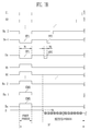
- FIG. 1 is a circuit diagram of a conventional pixel
- FIG. 2 shows driving waveforms applied to the conventional pixel
- FIG. 3 is a layout diagram showing an organic light emitting display according to an embodiment of the present invention.
- FIG. 4 is a circuit diagram of a pixel according to an embodiment of the present invention.
- FIGs. 5A and 5B show first driving waveforms applied to a pixel according to an embodiment of the present invention
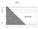
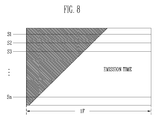
- FIG. 6 shows the length of emission times of pixels according to an embodiment of the present invention when the first driving waveforms of FIGs. 5A and 5B are applied;
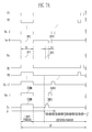
- FIGs. 7A and 7B show second driving waveforms applied to a pixel according to an embodiment of the present invention.
- FIG. 8 shows the length of emission times of pixels according to an embodiment of the present invention when the second driving waveforms of FIGs. 7A and 7B are applied.
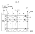
- FIG. 3 illustrates an organic light emitting display according to an embodiment of the present invention.
- an organic light emitting display includes a pixel portion 130 including a plurality of pixels 140 formed in regions where scan lines S 1 through Sn intersect (or cross) data lines D 1 through Dm; a scan driver 110 to drive the scan lines S 1 through Sn; a data driver 120 to drive the data lines D 1 through Dm; and a timing controller 150 to control the scan driver 110 and the data driver 120.
- the scan driver 110 receives a scan control signal SCS from the timing controller 150. In response to the scan control signal SCS, the scan driver 110 generates first scan signals and second scan signals. Here, the first scan signals are supplied to all scan lines S 1 through Sn at the same time, but the second scan signals are supplied to the first through n th scan lines S 1 through Sn in sequence. Further, the scan driver 110 generates first emission control signals and second emission control signals in response to the scan control signal SCS. Here, the first emission control signals are supplied to all emission control lines E1 through En at the same time, but the second emission control signals are supplied to the first through n th emission control lines E1 through En in sequence. Operations of the scan driver 110 will be described below in more detail.
- the data driver 120 receives a data control signal DCS from the timing controller 150. Then, the data driver 120 generates data signals in response to the data control signal DCS, and supplies data signals to the data lines D1 through Dm every time a respective one of the second scan signals is supplied. Further, the data driver 120 supplies a predetermined voltage to the data lines D 1 through Dm when the first scan signals are supplied to the scan lines S 1 through Sn. Detailed operations of the data driver 120 will be described below in more detail.
- the timing controller 150 generates the data control signal DCS and the scan control signal SCS in response to external synchronization signals.
- the timing controller 150 supplies the data control signal DCS and the scan control signal SCS to the data driver 120 and the scan driver 110, respectively. Further, the timing controller 150 supplies external data Data to the data driver 120.
- the pixel portion 130 includes the plurality of pixels 140.
- Each pixel 140 receives an external first power ELVDD and an external second power ELVSS, and emits light corresponding to a respective one of the data signals.
- FIG. 4 is a circuit diagram of a pixel according to an embodiment of the present invention.
- FIG. 4 illustrates the pixel 140 connected to the m th data line Dm, the (n-1) th scan line Sn-1, and the n th scan line Sn.
- the pixel 140 includes a pixel circuit 142 connected to the m th data line Dm, the (n-1) th scan line Sn-1, the n th scan line Sn, and the n th emission control line En, and controlling an organic light emitting diode OLED.
- the organic light emitting diode OLED includes an anode electrode connected to the pixel circuit 142, and a cathode electrode connected to a second power source ELVSS.
- the second power ELVSS has a lower voltage than a first power ELVDD; e.g., the second power ELVSS has a ground voltage.
- the organic light emitting diode OLED emits light corresponding to a current supplied from the pixel circuit 142.
- the pixel circuit 142 includes first and fifth transistors M1' and M5' connected between the first power source ELVDD and the organic light emitting diode OLED; a second transistor M2' and a first capacitor C1' connected between the first transistor M1' and the m th data line Dm'; third and fourth transistors M3' and M4'; and a second capacitor C2' connected between first and gate electrodes of the first transistor M1'.
- the second transistor M2' includes a first electrode connected to the m th data line Dm, a gate electrode connected to the n th scan line Sn, and a second electrode connected to a first terminal of the first capacitor C1'.
- the second transistor M2' is turned on when a respective one of the second scan signals is transmitted to the n th scan line Sn, and supplies a respective one of the data signals from the m th data line to the first terminal of the first capacitor C1'.
- the first transistor M1' includes the gate electrode connected to a first node N1, the first electrode connected to the first power source ELVDD, and a second electrode connected to a first electrode of the fifth transistor M5'.
- the first transistor M1' supplies a current corresponding to a voltage stored in the first and second capacitors C1' and C2' to the fifth transistor M5'.
- the third transistor M3' includes a gate electrode connected to the (n-1) th scan line Sn-1, a first electrode connected to the first node N1, and a second electrode connected to a first electrode of the fourth transistor M4'.
- the third transistor M3' is turned on when a respective one of the first scan signals or a respective one of the second scan signals is supplied to the (n-1) th scan line Sn-1.
- the fourth transistor M4' includes a gate electrode connected to the n th scan line Sn, the first electrode connected to the second electrode of the third transistor M3', and a second electrode connected to the first electrode of the fourth transistor M4'.
- the fourth transistor M4' is turned on when a respective one of the first scan signals or a respective one of the second scan signals is supplied to the n th scan line Sn.
- the third transistor M3' and the fourth transistor M4' are connected between the gate electrode and the second electrode of the first transistor M1'.
- the first transistor M1' is connected like a diode.
- the third transistor M3' and the fourth transistor M4' are controlled by different scan lines Sn-1 and Sn, so that the current flowing from the first node N1 to the first electrode of the fifth transistor M5' is prevented from leaking, which will be described later in more detail.
- the fifth transistor M5 includes a gate electrode connected to the n th emission control line En, the first electrode connected to both the second electrodes of the first and fourth transistors M1' and M4', and a second electrode connected to the anode electrode of the organic light emitting diode OLED.
- the fifth transistor M5' is turned off only when a respective one of the first emission control signals or a respective one of the second emission control signals is supplied to the n th emission control line En.
- the first and second capacitors C1' and C2' are each charged with a voltage corresponding to the threshold voltage of the first transistor M1' and the respective one of the data signals, and supply the charged voltage to the gate electrode of the first transistor M1'.
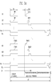
- FIGs. 5A and 5B show first driving waveforms applied to a pixel according to an embodiment of the present invention.
- one frame 1F is divided into a first period and a second period.
- the threshold voltage of the first transistor M1' provided in each pixel 140 is compensated.
- the second period a respective one of the data signals is supplied to each pixel 140, thereby displaying an image with desired brightness.
- the scan driver 110 supplies the first scan signals SP1 to all scan lines S1 through Sn at the same time.
- the scan driver 110 supplies the second scan signals SP2 to the first scan line S 1 through the n th scan line Sn in sequence.
- the width T1 of each of the first scan signals SP1 is wider than the width T2 of each of the second scan signals SP2 so as to fully compensate the threshold voltage of the first transistor M1'. That is, the time of applying each of the first scan signals SP1 is longer than the time of applying each of the second scan signals SP2.
- the scan driver 110 supplies the first emission control signals EMI1 to the emission control lines E1 through En during the first period. As the first emission control signals EMI1 are supplied, the fifth transistor M5' provided in each pixel 140 is turned off. Further, the scan driver 110 supplies the second emission control signals EMI2 to the first emission control line E1 through the n th emission control line En in sequence during the second period.
- the width of each of the first emission control signals EMI1 is wider than the width of each of the second emission control signal EMI2. That is, the time of applying each of the first emission control signals EMI1 is longer than the time of applying each of the second emission control signals EMI2.
- the data driver 120 supplies a predetermined voltage V1 to all data lines D1 through Dm in order to stably compensate the threshold voltage of the first transistor M1'.
- the voltage V1 is higher than the highest voltage of the data signals supplied from the data driver 120.
- the voltage V1 is set to be higher than the 4V.
- the voltage V1 may be equal to the voltages of the first power ELVDD.
- the data driver 120 supplies data signals DS to the data lines D1 through Dm to be synchronized with the second scan signals SP2.
- the pixel 140 operates as follows. During the first period, the first scan signals SP1 are supplied to all scan lines S1 through Sn, and at the same time the first emission control signals EMI1 are supplied to all emission control lines En. Further, the voltage V1 is supplied to all data lines D 1 through Dm in the first period. Here, for the sake of convenience, it is assumed that the voltage V1 is equal to the voltage of the first power ELVDD.
- the second, third and fourth transistors M2', M3' and M4' are turned on.
- the third and fourth transistors M3' and M4' are turned on, the first transistor M1' is connected like a diode. Therefore, a voltage obtained by subtracting the threshold voltage of the first transistor M1' from the first power ELVDD is applied to the first node N1.
- the second transistor M2' is also turned on, so that the voltage V1 (having the same level as the voltage of the first power ELVDD) is supplied to the first terminal of the first capacitor C1'. Then, the first capacitor C1' is charged with a voltage corresponding to the threshold voltage of the first transistor M1'.
- the second capacitor C2' is charged with a voltage corresponding to the difference between the voltage applied to the first node N1 and the voltage of the first power ELVDD. That is, the second capacitor C2' is charged with the threshold voltage of the first transistor M1'.
- the width (or time) T1 for applying each of the first scan signals SP1 is set to stably charge the first and second capacitors C1' and C2' with enough voltage. Therefore, the threshold voltage of the first transistor M1' is stably compensated during the first period. According to an embodiment of the present invention, the threshold voltage is not compensated while the second scan signals SP2 are supplied to the scan lines S 1 through Sn in sequence but is instead compensated during the separate first period, so that the first period can be set to be long enough to stably compensate the threshold voltage of the first transistor M1'.
- the second scan signals SP2 are sequentially supplied to the scan lines S1 though Sn, and at the same time the second emission control signals EMI2 are sequentially supplied to the emission control lines E1 through En. Further, in the second period, the data signals DS are supplied to the data lines D1 through Dm while synchronizing with the second scan signals SP2.
- the third transistor M3' When the respective one of the second scan signals SP2 is supplied to the (n-1) th scan line Sn-1, the third transistor M3' is turned on. At this time, the second transistor M2' and the fourth transistor M4' are kept being turned off. Therefore, even though the third transistor M3' is turned on, the leakage current due to the voltage charged in the first and second capacitors C1' and C2' is not supplied to the fifth transistor M4'. That is, in the second period, the third and fourth transistors M3' and M4' are turned on at different times, thereby preventing the leakage current due to the voltage charged in the first and second capacitors C1' and C2'.
- the second transistor M2' and the fourth transistor M4' are turned on.
- the voltage corresponding to the respective one of the data signals DS is charged in the first and second capacitors C1' and C2'.
- the voltage applied to the gate and source electrodes of the first transistor M1' is determined by the following equation 2 in consideration of the voltage previously charged in the first and second capacitors C1' and C2'.
- V g s VDD ⁇
- Vgs is a voltage applied to the gate and first electrodes of the first transistor M1'; Vth is the threshold voltage of the first transistor M1'; Vdata is a voltage of the data signal; C1 is the capacitance of the first capacitor C1'; and C2 is the capacitance of the second capacitor C2'.
- the threshold voltage Vth is canceled by substituting the Vgs of the equation 2 for that of the equation 1. In result, an image can be displayed with uniform brightness regardless of the threshold voltage of the first transistor M1'.
- the first transistor M1' supplies a current corresponding to the voltage stored in the first and second capacitors C1' and C2' to the first electrode of the fifth transistor M5'.
- the respective one of the second emission control signals EMI2 is supplied to the n th emission control line En.
- the fifth transistor M5' is turned off, thereby interrupting the current flowing to the organic light emitting diode OLED when the respective one of the second scan signals SP2 is supplied to the n th scan line Sn.
- the respective one of the second emission control signals EMI2 is stopped from being supplied to the n th emission control line En, thereby turning on the fifth transistor M5'. Then, the current is supplied from the first transistor M1' to the organic light emitting diode OLED, so that the organic light emitting diode OLED emits light with predetermined brightness.
- the first emission control signals EMI1 are supplied to the emission control lines E1 through En in the first period, but the second emission control signals EMI2 are not supplied to the emission control lines E1 through En in the second period.
- the threshold voltage of the first transistor M1' is compensated during the separate first period, so that an image is stably displayed even though the second emission control signals EMI2 are not supplied in the second period.
- the first through n th emission control lines E1 through En receive uniform driving waveforms, the first through n th emission control lines E1 through En can be commonly connected to one another.
- the respective pixels 140 have different periods (or lengths) of emission time according to scanning sequence of the second scan signals SP2. That is, while the driving waveforms are supplied as shown in FIGs. 5A and 5B, the period of the emission time for an emitting pixel 140 decreases as the emitting pixel 140 moves from being the pixel 140 connected to the first scan line S1 to the pixel 140 connected to the n th scan line Sn.
- the first and second capacitors C1' and C2' of each pixel 140 are charged with the voltage corresponding to the respective one of data signals of when the respective one of second scan signals SP2 is supplied.
- a respective one of the pixels 140 emits light from the time when its second scan signal SP2 is supplied.
- the voltage charged in the first and second capacitors C1' and C2' is changed into the voltage corresponding to the threshold voltage of the first transistor M1' when the respective one of the first scan signals SP1 is supplied. Therefore, the length of the emission time for each pixel 140 is related to a point of time when the respective one of the second scan signals SP2 is supplied and a point of time when the respective one of the first scan signals SP1 is supplied.
- the second scan signals SP2 are sequentially supplied to the first scan line S1 through the n th scan line Sn, so that the pixels 140 have different periods of the emission time.
- the pixel 140 first receiving its second scan signal SP2 has a longer emission time than the pixel 140 later receiving its second scan signal SP2.
- an embodiment of the present invention provides scanning sequences of the second scan signals SP2 that are alternately inversed between an odd-numbered frame and an even-numbered frame. That is, for example, in the odd-numbered frame, the scan driver 100 supplies the second scan signals SP2 in sequence from the first scan line S1 to the n th scan line Sn (refer to FIGs. 5A and 5B). On the other hand, in the even-numbered frame, the scan driver 100 supplies the second scan signals SP2 in sequence from the n th scan line Sn to the first scan line S1. In the case where the supply of the second scan signal SP2 is started at the n th scan line Sn as shown in FIGs.
- the period of emission time for an emitting pixel 140 decreases as the emitting pixel 140 moves from being the pixel 140 connected to the n th scan line Sn to the pixel 140 connected to the first scan line S 1 as shown in FIG. 8.
- the periods of the emission times for respective pixels 140 are equalized on the average. For example, when a pixel 140 has a relatively short emission time in the odd-numbered frame, it has a relatively long emission time in the even-numbered frame. Thus, the periods of the emission times for respective pixels 140 are equalized on the average, thereby displaying an image with uniform brightness.
- the second emission control signals EMI2 have the same supplying sequence as the second scan signals SP2.
- the second emission control signals EMI2 are also supplied in sequence of from the n th emission control line En to the first emission control line E1.
- the second emission control signals EMI2 are not supplied in the second period.
- the second scan signals SP2 may be supplied in sequence of from the first scan line S1 to the n th scan line Sn (refer to FIGs. 5A and 5B); and, in the odd-numbered frame, the second scan signals SP2 may be supplied in sequence of from the n th scan line Sn to the first scan line S1.
- the present invention provides an organic light emitting display and a driving method thereof, in which a voltage corresponding to a threshold voltage of a first transistor is charged in first and second capacitors of a pixel in a first period of one frame, thereby compensating differences between threshold voltages of a plurality of first transistors.
- the organic light emitting display can display an image with uniform brightness.
- the first period is set to fully compensate the threshold voltage of the first transistor, thereby stably compensating the threshold voltage of the first transistor.
- two other transistors are provided between a gate terminal and a second terminal of the first transistor and connected to different scan lines, thereby preventing a leakage current.
- scanning sequences of second scan signals are alternately inversed between an odd-numbered frame and an even-numbered frame, thereby equalizing the period of emission time for all pixels on the average.
Applications Claiming Priority (1)
| Application Number | Priority Date | Filing Date | Title |
|---|---|---|---|
| KR1020040090400A KR100592646B1 (ko) | 2004-11-08 | 2004-11-08 | 발광 표시장치 및 그의 구동방법 |
Publications (3)
| Publication Number | Publication Date |
|---|---|
| EP1655719A2 true EP1655719A2 (de) | 2006-05-10 |
| EP1655719A3 EP1655719A3 (de) | 2006-08-09 |
| EP1655719B1 EP1655719B1 (de) | 2009-06-24 |
Family
ID=35462511
Family Applications (1)
| Application Number | Title | Priority Date | Filing Date |
|---|---|---|---|
| EP05110397A Active EP1655719B1 (de) | 2004-11-08 | 2005-11-07 | Organische elektrolumineszente Anzeigevorrichtung und Ansteuerverfahren dafür |
Country Status (6)
| Country | Link |
|---|---|
| US (1) | US8354984B2 (de) |
| EP (1) | EP1655719B1 (de) |
| JP (1) | JP4509851B2 (de) |
| KR (1) | KR100592646B1 (de) |
| CN (1) | CN100409293C (de) |
| DE (1) | DE602005015070D1 (de) |
Cited By (3)
| Publication number | Priority date | Publication date | Assignee | Title |
|---|---|---|---|---|
| EP1947633A3 (de) * | 2007-01-16 | 2010-06-02 | Samsung Mobile Display Co., Ltd. | Organische lichtemittierende Anzeige |
| US8274452B2 (en) | 2007-01-16 | 2012-09-25 | Samsung Mobile Display Co., Ltd | Organic light emitting display having compensation for transistor threshold variation |
| CN106297706A (zh) * | 2016-09-01 | 2017-01-04 | 京东方科技集团股份有限公司 | 像素单元、显示基板、显示设备、驱动像素电极的方法 |
Families Citing this family (59)
| Publication number | Priority date | Publication date | Assignee | Title |
|---|---|---|---|---|
| US7503253B2 (en) * | 2004-02-09 | 2009-03-17 | Bunn-O-Matic Corporation | Apparatus, system and method for infusing a pre-packaged pod |
| KR100560445B1 (ko) * | 2004-03-15 | 2006-03-13 | 삼성에스디아이 주식회사 | 발광 표시 장치 및 그 구동 방법 |
| KR100560446B1 (ko) | 2004-03-15 | 2006-03-13 | 삼성에스디아이 주식회사 | 발광 표시 장치 및 그 구동 방법 |
| KR100662998B1 (ko) * | 2005-11-04 | 2006-12-28 | 삼성에스디아이 주식회사 | 유기 전계발광 표시장치 및 그 구동방법 |
| US9489891B2 (en) * | 2006-01-09 | 2016-11-08 | Ignis Innovation Inc. | Method and system for driving an active matrix display circuit |
| JP4735328B2 (ja) * | 2006-02-28 | 2011-07-27 | セイコーエプソン株式会社 | 電気光学装置および電子機器 |
| JP2007323036A (ja) | 2006-06-05 | 2007-12-13 | Samsung Sdi Co Ltd | 有機電界発光表示装置及びその駆動方法 |
| KR100793557B1 (ko) * | 2006-06-05 | 2008-01-14 | 삼성에스디아이 주식회사 | 유기전계발광표시장치 및 그의 구동방법 |
| CN100452158C (zh) * | 2006-10-12 | 2009-01-14 | 友达光电股份有限公司 | 用于一显示阵列的驱动控制装置及方法 |
| US20080136766A1 (en) * | 2006-12-07 | 2008-06-12 | George Lyons | Apparatus and Method for Displaying Image Data |
| KR20080064926A (ko) * | 2007-01-06 | 2008-07-10 | 삼성전자주식회사 | 표시 장치 및 그 구동 방법 |
| JP4428436B2 (ja) * | 2007-10-23 | 2010-03-10 | ソニー株式会社 | 表示装置および電子機器 |
| JP5186888B2 (ja) * | 2007-11-14 | 2013-04-24 | ソニー株式会社 | 表示装置及びその駆動方法と電子機器 |
| JP5287111B2 (ja) * | 2007-11-14 | 2013-09-11 | ソニー株式会社 | 表示装置及びその駆動方法と電子機器 |
| JP2009237041A (ja) * | 2008-03-26 | 2009-10-15 | Sony Corp | 画像表示装置及び画像表示方法 |
| JP2009244665A (ja) * | 2008-03-31 | 2009-10-22 | Sony Corp | パネルおよび駆動制御方法 |
| CN101556770B (zh) * | 2008-04-10 | 2011-09-21 | 联咏科技股份有限公司 | 用于一液晶显示器降低电源噪声的驱动方法及其相关装置 |
| JP2010002498A (ja) | 2008-06-18 | 2010-01-07 | Sony Corp | パネルおよび駆動制御方法 |
| JP2010002495A (ja) * | 2008-06-18 | 2010-01-07 | Sony Corp | パネルおよび駆動制御方法 |
| KR101481667B1 (ko) * | 2008-07-08 | 2015-01-13 | 엘지디스플레이 주식회사 | 발광 표시 장치 및 이의 구동 방법 |
| KR101064381B1 (ko) * | 2009-07-29 | 2011-09-14 | 삼성모바일디스플레이주식회사 | 유기전계발광 표시장치 |
| KR101178911B1 (ko) * | 2009-10-15 | 2012-09-03 | 삼성디스플레이 주식회사 | 화소 및 이를 이용한 유기전계발광 표시장치 |
| JP4801794B2 (ja) * | 2009-11-27 | 2011-10-26 | パナソニック株式会社 | 発光表示装置 |
| KR101048985B1 (ko) * | 2010-02-09 | 2011-07-12 | 삼성모바일디스플레이주식회사 | 화소 및 이를 이용한 유기전계발광 표시장치 |
| KR101452655B1 (ko) | 2010-07-12 | 2014-10-22 | 샤프 가부시키가이샤 | 표시 장치 및 그 구동 방법 |
| JP5456901B2 (ja) * | 2010-09-06 | 2014-04-02 | パナソニック株式会社 | 表示装置およびその駆動方法 |
| JP5721736B2 (ja) * | 2010-10-21 | 2015-05-20 | シャープ株式会社 | 表示装置およびその駆動方法 |
| KR101738920B1 (ko) * | 2010-10-28 | 2017-05-24 | 삼성디스플레이 주식회사 | 유기전계발광 표시장치 |
| KR101783898B1 (ko) * | 2010-11-05 | 2017-10-11 | 삼성디스플레이 주식회사 | 화소 및 이를 이용한 유기전계발광 표시장치 |
| KR101813192B1 (ko) * | 2011-05-31 | 2017-12-29 | 삼성디스플레이 주식회사 | 화소 및 이를 포함하는 표시장치, 및 그 구동방법 |
| KR20130046006A (ko) * | 2011-10-27 | 2013-05-07 | 삼성디스플레이 주식회사 | 화소 회로, 이를 포함하는 유기 발광 표시 장치 및 유기 발광 표시 장치의 구동 방법 |
| JP5890656B2 (ja) * | 2011-11-09 | 2016-03-22 | 三星ディスプレイ株式會社Samsung Display Co.,Ltd. | 電気光学装置の駆動方法および電気光学装置 |
| KR101966910B1 (ko) * | 2011-11-18 | 2019-08-14 | 삼성디스플레이 주식회사 | 표시장치 및 그 구동 방법 |
| KR101875123B1 (ko) * | 2012-02-28 | 2018-07-09 | 삼성디스플레이 주식회사 | 화소 및 이를 이용한 유기전계발광 표시장치 |
| TWI460704B (zh) * | 2012-03-21 | 2014-11-11 | Innocom Tech Shenzhen Co Ltd | 顯示器及其驅動方法 |
| KR101893167B1 (ko) * | 2012-03-23 | 2018-10-05 | 삼성디스플레이 주식회사 | 화소 회로, 이의 구동 방법 및 유기 발광 표시 장치 |
| KR101995218B1 (ko) * | 2012-03-27 | 2019-07-02 | 엘지디스플레이 주식회사 | 유기발광 표시장치 |
| JP6074585B2 (ja) * | 2012-07-31 | 2017-02-08 | 株式会社Joled | 表示装置および電子機器、ならびに表示パネルの駆動方法 |
| JP5961125B2 (ja) * | 2013-02-26 | 2016-08-02 | 株式会社ジャパンディスプレイ | 表示装置及び電子機器 |
| JP2014197120A (ja) * | 2013-03-29 | 2014-10-16 | ソニー株式会社 | 表示装置、cmos演算増幅器及び表示装置の駆動方法 |
| KR101993747B1 (ko) * | 2013-04-02 | 2019-07-02 | 삼성디스플레이 주식회사 | 유기전계발광 표시장치 및 그의 구동방법 |
| CN103280187B (zh) * | 2013-06-09 | 2015-12-23 | 上海和辉光电有限公司 | 像素排列显示方法、装置及oled显示器 |
| KR20150057547A (ko) * | 2013-11-20 | 2015-05-28 | 삼성디스플레이 주식회사 | 유기전계발광 표시장치 |
| KR102147055B1 (ko) * | 2014-02-05 | 2020-08-24 | 삼성디스플레이 주식회사 | 액정 표시 장치 및 이의 구동 방법 |
| KR102206608B1 (ko) | 2014-03-19 | 2021-01-25 | 삼성디스플레이 주식회사 | 유기전계발광 표시장치 및 그의 구동방법 |
| CN104252841B (zh) * | 2014-09-15 | 2017-03-08 | 西安诺瓦电子科技有限公司 | Led显示控制方法及控制卡、led显示屏系统 |
| KR102230928B1 (ko) * | 2014-10-13 | 2021-03-24 | 삼성디스플레이 주식회사 | 유기 발광 표시 장치 및 이의 구동 방법 |
| KR102218653B1 (ko) * | 2015-02-12 | 2021-02-23 | 삼성디스플레이 주식회사 | 표시 장치의 게이트 드라이버 및 표시 장치 |
| CN104575440A (zh) * | 2015-02-15 | 2015-04-29 | 京东方科技集团股份有限公司 | 一种显示驱动电路及其驱动方法、显示装置 |
| CN104778921B (zh) * | 2015-04-24 | 2018-08-07 | 广东威创视讯科技股份有限公司 | 一种led显示屏译码行选电路及led显示屏控制系统 |
| CN105261340A (zh) * | 2015-11-09 | 2016-01-20 | 武汉华星光电技术有限公司 | Goa驱动电路、tft显示面板及显示装置 |
| KR102526724B1 (ko) * | 2016-05-19 | 2023-05-02 | 삼성디스플레이 주식회사 | 표시 장치 |
| KR20180098442A (ko) * | 2017-02-24 | 2018-09-04 | 삼성디스플레이 주식회사 | 화소 및 이를 가지는 유기전계발광 표시장치 |
| KR20200115766A (ko) * | 2019-03-25 | 2020-10-08 | 삼성디스플레이 주식회사 | 표시 장치 및 그의 구동 방법 |
| CN110969976B (zh) * | 2019-11-29 | 2023-03-10 | 厦门天马微电子有限公司 | 显示装置的驱动方法和显示装置 |
| CN113808519B (zh) * | 2020-06-17 | 2023-11-21 | 成都辰显光电有限公司 | 像素电路及其驱动方法、显示面板 |
| EP4174836A4 (de) * | 2020-10-20 | 2023-12-13 | Samsung Electronics Co., Ltd. | Anzeigegerät |
| CN112234091A (zh) * | 2020-10-23 | 2021-01-15 | 厦门天马微电子有限公司 | 显示面板和显示装置 |
| CN112509476B (zh) * | 2020-11-30 | 2022-10-21 | 錼创显示科技股份有限公司 | 微发光二极管显示装置 |
Citations (2)
| Publication number | Priority date | Publication date | Assignee | Title |
|---|---|---|---|---|
| EP0478186A2 (de) | 1990-09-25 | 1992-04-01 | THORN EMI plc | Anzeigeeinrichtung |
| US20040046719A1 (en) | 2002-08-16 | 2004-03-11 | Wen-Chun Wang | Active organic light emitting diode drive circuit |
Family Cites Families (15)
| Publication number | Priority date | Publication date | Assignee | Title |
|---|---|---|---|---|
| JPH05265403A (ja) * | 1992-03-17 | 1993-10-15 | Fujitsu Ltd | カラー液晶表示装置 |
| US6229506B1 (en) | 1997-04-23 | 2001-05-08 | Sarnoff Corporation | Active matrix light emitting diode pixel structure and concomitant method |
| JP3168974B2 (ja) * | 1998-02-24 | 2001-05-21 | 日本電気株式会社 | 液晶表示装置の駆動方法と、それを用いた液晶表示装置 |
| US6847341B2 (en) | 2000-04-19 | 2005-01-25 | Semiconductor Energy Laboratory Co., Ltd. | Electronic device and method of driving the same |
| JP3494140B2 (ja) | 2000-09-18 | 2004-02-03 | 日本電気株式会社 | 液晶表示装置の駆動方法と、それを用いた液晶表示装置 |
| JP2002351401A (ja) * | 2001-03-21 | 2002-12-06 | Mitsubishi Electric Corp | 自発光型表示装置 |
| JP5044876B2 (ja) * | 2001-05-31 | 2012-10-10 | パナソニック株式会社 | 液晶表示装置の駆動方法および液晶表示装置 |
| JP3800404B2 (ja) * | 2001-12-19 | 2006-07-26 | 株式会社日立製作所 | 画像表示装置 |
| JP2003216100A (ja) * | 2002-01-21 | 2003-07-30 | Matsushita Electric Ind Co Ltd | El表示パネルとel表示装置およびその駆動方法および表示装置の検査方法とel表示装置のドライバ回路 |
| JP2003295826A (ja) | 2002-04-03 | 2003-10-15 | Sanyo Electric Co Ltd | 有機el表示装置 |
| JP2004093682A (ja) * | 2002-08-29 | 2004-03-25 | Toshiba Matsushita Display Technology Co Ltd | El表示パネル、el表示パネルの駆動方法、el表示装置の駆動回路およびel表示装置 |
| JP2004279990A (ja) * | 2003-03-19 | 2004-10-07 | Toshiba Matsushita Display Technology Co Ltd | El表示装置 |
| JP2004294752A (ja) * | 2003-03-27 | 2004-10-21 | Toshiba Matsushita Display Technology Co Ltd | El表示装置 |
| US7196682B2 (en) * | 2003-09-29 | 2007-03-27 | Wintek Corporation | Driving apparatus and method for active matrix organic light emitting display |
| US7173585B2 (en) * | 2004-03-10 | 2007-02-06 | Wintek Corporation | Active matrix display driving circuit |
-
2004
- 2004-11-08 KR KR1020040090400A patent/KR100592646B1/ko active IP Right Grant
-
2005
- 2005-05-11 JP JP2005139155A patent/JP4509851B2/ja active Active
- 2005-10-07 US US11/245,997 patent/US8354984B2/en active Active
- 2005-11-07 EP EP05110397A patent/EP1655719B1/de active Active
- 2005-11-07 DE DE602005015070T patent/DE602005015070D1/de active Active
- 2005-11-08 CN CNB2005101203112A patent/CN100409293C/zh active Active
Patent Citations (2)
| Publication number | Priority date | Publication date | Assignee | Title |
|---|---|---|---|---|
| EP0478186A2 (de) | 1990-09-25 | 1992-04-01 | THORN EMI plc | Anzeigeeinrichtung |
| US20040046719A1 (en) | 2002-08-16 | 2004-03-11 | Wen-Chun Wang | Active organic light emitting diode drive circuit |
Cited By (6)
| Publication number | Priority date | Publication date | Assignee | Title |
|---|---|---|---|---|
| EP1947633A3 (de) * | 2007-01-16 | 2010-06-02 | Samsung Mobile Display Co., Ltd. | Organische lichtemittierende Anzeige |
| US8232933B2 (en) | 2007-01-16 | 2012-07-31 | Samsung Mobile Display Co., Ltd. | Organic light emitting display with compensation for transistor threshold variation |
| US8274452B2 (en) | 2007-01-16 | 2012-09-25 | Samsung Mobile Display Co., Ltd | Organic light emitting display having compensation for transistor threshold variation |
| CN106297706A (zh) * | 2016-09-01 | 2017-01-04 | 京东方科技集团股份有限公司 | 像素单元、显示基板、显示设备、驱动像素电极的方法 |
| CN106297706B (zh) * | 2016-09-01 | 2017-10-31 | 京东方科技集团股份有限公司 | 像素单元、显示基板、显示设备、驱动像素电极的方法 |
| US10573268B2 (en) | 2016-09-01 | 2020-02-25 | Boe Technology Group Co., Ltd. | Pixel cell, display substrate, display device, and method of driving pixel electrode |
Also Published As
| Publication number | Publication date |
|---|---|
| JP2006133731A (ja) | 2006-05-25 |
| CN100409293C (zh) | 2008-08-06 |
| KR100592646B1 (ko) | 2006-06-26 |
| US20060097966A1 (en) | 2006-05-11 |
| EP1655719B1 (de) | 2009-06-24 |
| CN1773593A (zh) | 2006-05-17 |
| EP1655719A3 (de) | 2006-08-09 |
| DE602005015070D1 (de) | 2009-08-06 |
| US8354984B2 (en) | 2013-01-15 |
| KR20060041046A (ko) | 2006-05-11 |
| JP4509851B2 (ja) | 2010-07-21 |
Similar Documents
| Publication | Publication Date | Title |
|---|---|---|
| US8354984B2 (en) | Organic light emitting display and driving method thereof | |
| EP2410508B1 (de) | Pixel und organische lichtemittierende Anzeige damit | |
| EP1887552B1 (de) | Organische lichtemittierende Anzeigevorrichtung | |
| EP2261884B1 (de) | Pixel einer OLED Anzeige und entsprechende Anzeige | |
| KR101693693B1 (ko) | 화소 및 이를 이용한 유기전계발광 표시장치 | |
| KR100732828B1 (ko) | 화소 및 이를 이용한 발광 표시장치 | |
| US8780102B2 (en) | Pixel, display device, and driving method thereof | |
| US7847760B2 (en) | Pixel circuit, organic light emitting display using the pixel circuit and driving method for the display | |
| EP2747064B1 (de) | Organische lichtemittierende Diodenanzeigevorrichtung und Ansteuerungsverfahren dafür | |
| US9105213B2 (en) | Organic light emitting diode display and method of driving the same | |
| US8242980B2 (en) | Pixel circuit configured to provide feedback to a drive transistor, display including the same, and driving method thereof | |
| KR101142729B1 (ko) | 화소 및 이를 이용한 유기전계발광 표시장치 | |
| US10692427B2 (en) | Pixel and organic light emitting display device using the pixel | |
| KR101765778B1 (ko) | 유기전계발광 표시장치 | |
| EP2219174A1 (de) | Pixel und organische lichtemittierende Anzeigevorrichtung damit | |
| EP2736036A2 (de) | Organische lichtemittierende Diodenanzeigevorrichtung und Ansteuerungsverfahren dafür | |
| EP1887551A1 (de) | Organische lichtemittierende Anzeigevorrichtung | |
| US9330603B2 (en) | Organic light emitting diode display device and method of driving the same | |
| US20120105408A1 (en) | Organic light emitting display | |
| EP1895497A1 (de) | Pixel und elektrolumineszente Anzeigen damit | |
| US9491829B2 (en) | Organic light emitting diode display and method of driving the same | |
| US9047816B2 (en) | Pixel and organic light emitting display device using the same | |
| KR100707624B1 (ko) | 화소 및 이를 이용한 발광 표시장치와 그의 구동방법 | |
| KR101928018B1 (ko) | 화소 및 이를 이용한 유기전계발광 표시장치 | |
| KR100592645B1 (ko) | 화소 및 이를 이용한 발광 표시장치와 그의 구동방법 |
Legal Events
| Date | Code | Title | Description |
|---|---|---|---|
| PUAI | Public reference made under article 153(3) epc to a published international application that has entered the european phase |
Free format text: ORIGINAL CODE: 0009012 |
|
| AK | Designated contracting states |
Kind code of ref document: A2 Designated state(s): AT BE BG CH CY CZ DE DK EE ES FI FR GB GR HU IE IS IT LI LT LU LV MC NL PL PT RO SE SI SK TR |
|
| AX | Request for extension of the european patent |
Extension state: AL BA HR MK YU |
|
| PUAL | Search report despatched |
Free format text: ORIGINAL CODE: 0009013 |
|
| AK | Designated contracting states |
Kind code of ref document: A3 Designated state(s): AT BE BG CH CY CZ DE DK EE ES FI FR GB GR HU IE IS IT LI LT LU LV MC NL PL PT RO SE SI SK TR |
|
| AX | Request for extension of the european patent |
Extension state: AL BA HR MK YU |
|
| 17P | Request for examination filed |
Effective date: 20070208 |
|
| AKX | Designation fees paid |
Designated state(s): DE FR GB |
|
| 17Q | First examination report despatched |
Effective date: 20080516 |
|
| GRAP | Despatch of communication of intention to grant a patent |
Free format text: ORIGINAL CODE: EPIDOSNIGR1 |
|
| RAP1 | Party data changed (applicant data changed or rights of an application transferred) |
Owner name: SAMSUNG MOBILE DISPLAY CO., LTD. |
|
| RIN1 | Information on inventor provided before grant (corrected) |
Inventor name: CHOI, SANG MOO |
|
| GRAS | Grant fee paid |
Free format text: ORIGINAL CODE: EPIDOSNIGR3 |
|
| GRAA | (expected) grant |
Free format text: ORIGINAL CODE: 0009210 |
|
| AK | Designated contracting states |
Kind code of ref document: B1 Designated state(s): DE FR GB |
|
| REG | Reference to a national code |
Ref country code: GB Ref legal event code: FG4D |
|
| REF | Corresponds to: |
Ref document number: 602005015070 Country of ref document: DE Date of ref document: 20090806 Kind code of ref document: P |
|
| PLBE | No opposition filed within time limit |
Free format text: ORIGINAL CODE: 0009261 |
|
| STAA | Information on the status of an ep patent application or granted ep patent |
Free format text: STATUS: NO OPPOSITION FILED WITHIN TIME LIMIT |
|
| 26N | No opposition filed |
Effective date: 20100325 |
|
| REG | Reference to a national code |
Ref country code: GB Ref legal event code: 732E Free format text: REGISTERED BETWEEN 20130103 AND 20130109 |
|
| REG | Reference to a national code |
Ref country code: DE Ref legal event code: R082 Ref document number: 602005015070 Country of ref document: DE Representative=s name: GULDE HENGELHAUPT ZIEBIG & SCHNEIDER, DE |
|
| REG | Reference to a national code |
Ref country code: DE Ref legal event code: R082 Ref document number: 602005015070 Country of ref document: DE Representative=s name: GULDE HENGELHAUPT ZIEBIG & SCHNEIDER, DE Effective date: 20130416 Ref country code: DE Ref legal event code: R081 Ref document number: 602005015070 Country of ref document: DE Owner name: SAMSUNG DISPLAY CO., LTD., KR Free format text: FORMER OWNER: SAMSUNG MOBILE DISPLAY CO. LTD., SUWON, KR Effective date: 20130416 Ref country code: DE Ref legal event code: R082 Ref document number: 602005015070 Country of ref document: DE Representative=s name: GULDE & PARTNER PATENT- UND RECHTSANWALTSKANZL, DE Effective date: 20130416 Ref country code: DE Ref legal event code: R081 Ref document number: 602005015070 Country of ref document: DE Owner name: SAMSUNG DISPLAY CO., LTD., YONGIN-CITY, KR Free format text: FORMER OWNER: SAMSUNG MOBILE DISPLAY CO. LTD., SUWON, GYEONGGI, KR Effective date: 20130416 |
|
| REG | Reference to a national code |
Ref country code: FR Ref legal event code: PLFP Year of fee payment: 11 |
|
| REG | Reference to a national code |
Ref country code: FR Ref legal event code: PLFP Year of fee payment: 12 |
|
| REG | Reference to a national code |
Ref country code: FR Ref legal event code: PLFP Year of fee payment: 13 |
|
| REG | Reference to a national code |
Ref country code: FR Ref legal event code: PLFP Year of fee payment: 14 |
|
| P01 | Opt-out of the competence of the unified patent court (upc) registered |
Effective date: 20230515 |
|
| PGFP | Annual fee paid to national office [announced via postgrant information from national office to epo] |
Ref country code: GB Payment date: 20231023 Year of fee payment: 19 |
|
| PGFP | Annual fee paid to national office [announced via postgrant information from national office to epo] |
Ref country code: FR Payment date: 20231024 Year of fee payment: 19 Ref country code: DE Payment date: 20231023 Year of fee payment: 19 |