EP1649685B1 - Cmos bildaufnehmer mit automatischer integrationszeitsteuerung und doppelter korrelierter abtastung - Google Patents
Cmos bildaufnehmer mit automatischer integrationszeitsteuerung und doppelter korrelierter abtastung Download PDFInfo
- Publication number
- EP1649685B1 EP1649685B1 EP04756394.5A EP04756394A EP1649685B1 EP 1649685 B1 EP1649685 B1 EP 1649685B1 EP 04756394 A EP04756394 A EP 04756394A EP 1649685 B1 EP1649685 B1 EP 1649685B1
- Authority
- EP
- European Patent Office
- Prior art keywords
- photo
- charge
- conversion devices
- charge generated
- pixel
- Prior art date
- Legal status (The legal status is an assumption and is not a legal conclusion. Google has not performed a legal analysis and makes no representation as to the accuracy of the status listed.)
- Expired - Lifetime
Links
- 238000005070 sampling Methods 0.000 title description 7
- 230000002596 correlated effect Effects 0.000 title description 6
- 238000003384 imaging method Methods 0.000 title description 5
- 238000006243 chemical reaction Methods 0.000 claims description 68
- 238000012544 monitoring process Methods 0.000 claims description 29
- 238000012546 transfer Methods 0.000 claims description 28
- 238000000034 method Methods 0.000 claims description 20
- 230000004044 response Effects 0.000 claims description 13
- 238000009792 diffusion process Methods 0.000 description 67
- 238000007667 floating Methods 0.000 description 63
- 239000010410 layer Substances 0.000 description 47
- 239000000758 substrate Substances 0.000 description 35
- 238000010586 diagram Methods 0.000 description 21
- VYPSYNLAJGMNEJ-UHFFFAOYSA-N silicon dioxide Inorganic materials O=[Si]=O VYPSYNLAJGMNEJ-UHFFFAOYSA-N 0.000 description 11
- 239000002344 surface layer Substances 0.000 description 9
- 239000002019 doping agent Substances 0.000 description 8
- 230000000875 corresponding effect Effects 0.000 description 7
- 230000008569 process Effects 0.000 description 6
- 239000004065 semiconductor Substances 0.000 description 6
- 239000003989 dielectric material Substances 0.000 description 5
- 238000002955 isolation Methods 0.000 description 5
- 238000004519 manufacturing process Methods 0.000 description 5
- 229910052751 metal Inorganic materials 0.000 description 5
- 239000002184 metal Substances 0.000 description 5
- XUIMIQQOPSSXEZ-UHFFFAOYSA-N Silicon Chemical compound [Si] XUIMIQQOPSSXEZ-UHFFFAOYSA-N 0.000 description 4
- 230000003287 optical effect Effects 0.000 description 4
- 229920002120 photoresistant polymer Polymers 0.000 description 4
- 229910021420 polycrystalline silicon Inorganic materials 0.000 description 4
- 229920005591 polysilicon Polymers 0.000 description 4
- 229910021332 silicide Inorganic materials 0.000 description 4
- FVBUAEGBCNSCDD-UHFFFAOYSA-N silicide(4-) Chemical compound [Si-4] FVBUAEGBCNSCDD-UHFFFAOYSA-N 0.000 description 4
- 229910052710 silicon Inorganic materials 0.000 description 4
- 239000010703 silicon Substances 0.000 description 4
- 239000000377 silicon dioxide Substances 0.000 description 4
- 229910052581 Si3N4 Inorganic materials 0.000 description 3
- 238000005229 chemical vapour deposition Methods 0.000 description 3
- 238000013461 design Methods 0.000 description 3
- 230000006870 function Effects 0.000 description 3
- 230000010354 integration Effects 0.000 description 3
- 239000000463 material Substances 0.000 description 3
- 238000002161 passivation Methods 0.000 description 3
- 238000012545 processing Methods 0.000 description 3
- 235000012239 silicon dioxide Nutrition 0.000 description 3
- HQVNEWCFYHHQES-UHFFFAOYSA-N silicon nitride Chemical compound N12[Si]34N5[Si]62N3[Si]51N64 HQVNEWCFYHHQES-UHFFFAOYSA-N 0.000 description 3
- 125000006850 spacer group Chemical group 0.000 description 3
- ZOXJGFHDIHLPTG-UHFFFAOYSA-N Boron Chemical compound [B] ZOXJGFHDIHLPTG-UHFFFAOYSA-N 0.000 description 2
- OAICVXFJPJFONN-UHFFFAOYSA-N Phosphorus Chemical compound [P] OAICVXFJPJFONN-UHFFFAOYSA-N 0.000 description 2
- 241000220010 Rhode Species 0.000 description 2
- 238000009825 accumulation Methods 0.000 description 2
- 230000003321 amplification Effects 0.000 description 2
- 229910052787 antimony Inorganic materials 0.000 description 2
- WATWJIUSRGPENY-UHFFFAOYSA-N antimony atom Chemical compound [Sb] WATWJIUSRGPENY-UHFFFAOYSA-N 0.000 description 2
- 229910052785 arsenic Inorganic materials 0.000 description 2
- RQNWIZPPADIBDY-UHFFFAOYSA-N arsenic atom Chemical compound [As] RQNWIZPPADIBDY-UHFFFAOYSA-N 0.000 description 2
- 230000008901 benefit Effects 0.000 description 2
- 230000015572 biosynthetic process Effects 0.000 description 2
- 229910052796 boron Inorganic materials 0.000 description 2
- 229910052681 coesite Inorganic materials 0.000 description 2
- 239000004020 conductor Substances 0.000 description 2
- 229910052906 cristobalite Inorganic materials 0.000 description 2
- 230000001066 destructive effect Effects 0.000 description 2
- 238000002513 implantation Methods 0.000 description 2
- 239000012212 insulator Substances 0.000 description 2
- 150000004767 nitrides Chemical class 0.000 description 2
- 238000003199 nucleic acid amplification method Methods 0.000 description 2
- 230000002093 peripheral effect Effects 0.000 description 2
- 229910052698 phosphorus Inorganic materials 0.000 description 2
- 239000011574 phosphorus Substances 0.000 description 2
- 229910052814 silicon oxide Inorganic materials 0.000 description 2
- 229910052682 stishovite Inorganic materials 0.000 description 2
- 238000003860 storage Methods 0.000 description 2
- 230000007704 transition Effects 0.000 description 2
- 229910052905 tridymite Inorganic materials 0.000 description 2
- 229910052721 tungsten Inorganic materials 0.000 description 2
- JBRZTFJDHDCESZ-UHFFFAOYSA-N AsGa Chemical compound [As]#[Ga] JBRZTFJDHDCESZ-UHFFFAOYSA-N 0.000 description 1
- 229910001218 Gallium arsenide Inorganic materials 0.000 description 1
- 229910000577 Silicon-germanium Inorganic materials 0.000 description 1
- BOTDANWDWHJENH-UHFFFAOYSA-N Tetraethyl orthosilicate Chemical compound CCO[Si](OCC)(OCC)OCC BOTDANWDWHJENH-UHFFFAOYSA-N 0.000 description 1
- ATJFFYVFTNAWJD-UHFFFAOYSA-N Tin Chemical compound [Sn] ATJFFYVFTNAWJD-UHFFFAOYSA-N 0.000 description 1
- LEVVHYCKPQWKOP-UHFFFAOYSA-N [Si].[Ge] Chemical compound [Si].[Ge] LEVVHYCKPQWKOP-UHFFFAOYSA-N 0.000 description 1
- 230000004888 barrier function Effects 0.000 description 1
- YXTPWUNVHCYOSP-UHFFFAOYSA-N bis($l^{2}-silanylidene)molybdenum Chemical compound [Si]=[Mo]=[Si] YXTPWUNVHCYOSP-UHFFFAOYSA-N 0.000 description 1
- 239000005380 borophosphosilicate glass Substances 0.000 description 1
- 230000008859 change Effects 0.000 description 1
- 239000002800 charge carrier Substances 0.000 description 1
- 239000010941 cobalt Substances 0.000 description 1
- 229910017052 cobalt Inorganic materials 0.000 description 1
- GUTLYIVDDKVIGB-UHFFFAOYSA-N cobalt atom Chemical compound [Co] GUTLYIVDDKVIGB-UHFFFAOYSA-N 0.000 description 1
- 238000010276 construction Methods 0.000 description 1
- 230000001276 controlling effect Effects 0.000 description 1
- 230000006378 damage Effects 0.000 description 1
- 238000013144 data compression Methods 0.000 description 1
- 238000000151 deposition Methods 0.000 description 1
- 238000001514 detection method Methods 0.000 description 1
- 230000005670 electromagnetic radiation Effects 0.000 description 1
- 238000005516 engineering process Methods 0.000 description 1
- 239000012634 fragment Substances 0.000 description 1
- 239000003574 free electron Substances 0.000 description 1
- 229910052732 germanium Inorganic materials 0.000 description 1
- GNPVGFCGXDBREM-UHFFFAOYSA-N germanium atom Chemical compound [Ge] GNPVGFCGXDBREM-UHFFFAOYSA-N 0.000 description 1
- 239000011521 glass Substances 0.000 description 1
- 239000007943 implant Substances 0.000 description 1
- 238000011065 in-situ storage Methods 0.000 description 1
- 229910052738 indium Inorganic materials 0.000 description 1
- APFVFJFRJDLVQX-UHFFFAOYSA-N indium atom Chemical compound [In] APFVFJFRJDLVQX-UHFFFAOYSA-N 0.000 description 1
- 150000002500 ions Chemical class 0.000 description 1
- 230000005055 memory storage Effects 0.000 description 1
- 238000001465 metallisation Methods 0.000 description 1
- 229910021344 molybdenum silicide Inorganic materials 0.000 description 1
- 239000006187 pill Substances 0.000 description 1
- 229920000642 polymer Polymers 0.000 description 1
- 238000005036 potential barrier Methods 0.000 description 1
- 238000003672 processing method Methods 0.000 description 1
- 239000011241 protective layer Substances 0.000 description 1
- 239000010453 quartz Substances 0.000 description 1
- 230000014624 response to red light Effects 0.000 description 1
- 229910052594 sapphire Inorganic materials 0.000 description 1
- 239000010980 sapphire Substances 0.000 description 1
- HBMJWWWQQXIZIP-UHFFFAOYSA-N silicon carbide Chemical compound [Si+]#[C-] HBMJWWWQQXIZIP-UHFFFAOYSA-N 0.000 description 1
- 229910010271 silicon carbide Inorganic materials 0.000 description 1
- LIVNPJMFVYWSIS-UHFFFAOYSA-N silicon monoxide Chemical compound [Si-]#[O+] LIVNPJMFVYWSIS-UHFFFAOYSA-N 0.000 description 1
- 230000006641 stabilisation Effects 0.000 description 1
- 238000011105 stabilization Methods 0.000 description 1
- 229910052715 tantalum Inorganic materials 0.000 description 1
- GUVRBAGPIYLISA-UHFFFAOYSA-N tantalum atom Chemical compound [Ta] GUVRBAGPIYLISA-UHFFFAOYSA-N 0.000 description 1
- 229910021341 titanium silicide Inorganic materials 0.000 description 1
- WQJQOUPTWCFRMM-UHFFFAOYSA-N tungsten disilicide Chemical compound [Si]#[W]#[Si] WQJQOUPTWCFRMM-UHFFFAOYSA-N 0.000 description 1
- 229910021342 tungsten silicide Inorganic materials 0.000 description 1
Images






Classifications
-
- H—ELECTRICITY
- H10—SEMICONDUCTOR DEVICES; ELECTRIC SOLID-STATE DEVICES NOT OTHERWISE PROVIDED FOR
- H10F—INORGANIC SEMICONDUCTOR DEVICES SENSITIVE TO INFRARED RADIATION, LIGHT, ELECTROMAGNETIC RADIATION OF SHORTER WAVELENGTH OR CORPUSCULAR RADIATION
- H10F39/00—Integrated devices, or assemblies of multiple devices, comprising at least one element covered by group H10F30/00, e.g. radiation detectors comprising photodiode arrays
- H10F39/80—Constructional details of image sensors
- H10F39/806—Optical elements or arrangements associated with the image sensors
- H10F39/8063—Microlenses
-
- H—ELECTRICITY
- H04—ELECTRIC COMMUNICATION TECHNIQUE
- H04N—PICTORIAL COMMUNICATION, e.g. TELEVISION
- H04N25/00—Circuitry of solid-state image sensors [SSIS]; Control thereof
- H04N25/60—Noise processing, e.g. detecting, correcting, reducing or removing noise
- H04N25/616—Noise processing, e.g. detecting, correcting, reducing or removing noise involving a correlated sampling function, e.g. correlated double sampling [CDS] or triple sampling
-
- H—ELECTRICITY
- H04—ELECTRIC COMMUNICATION TECHNIQUE
- H04N—PICTORIAL COMMUNICATION, e.g. TELEVISION
- H04N25/00—Circuitry of solid-state image sensors [SSIS]; Control thereof
- H04N25/70—SSIS architectures; Circuits associated therewith
- H04N25/76—Addressed sensors, e.g. MOS or CMOS sensors
- H04N25/77—Pixel circuitry, e.g. memories, A/D converters, pixel amplifiers, shared circuits or shared components
- H04N25/778—Pixel circuitry, e.g. memories, A/D converters, pixel amplifiers, shared circuits or shared components comprising amplifiers shared between a plurality of pixels, i.e. at least one part of the amplifier must be on the sensor array itself
-
- H—ELECTRICITY
- H10—SEMICONDUCTOR DEVICES; ELECTRIC SOLID-STATE DEVICES NOT OTHERWISE PROVIDED FOR
- H10F—INORGANIC SEMICONDUCTOR DEVICES SENSITIVE TO INFRARED RADIATION, LIGHT, ELECTROMAGNETIC RADIATION OF SHORTER WAVELENGTH OR CORPUSCULAR RADIATION
- H10F39/00—Integrated devices, or assemblies of multiple devices, comprising at least one element covered by group H10F30/00, e.g. radiation detectors comprising photodiode arrays
- H10F39/80—Constructional details of image sensors
-
- H—ELECTRICITY
- H10—SEMICONDUCTOR DEVICES; ELECTRIC SOLID-STATE DEVICES NOT OTHERWISE PROVIDED FOR
- H10F—INORGANIC SEMICONDUCTOR DEVICES SENSITIVE TO INFRARED RADIATION, LIGHT, ELECTROMAGNETIC RADIATION OF SHORTER WAVELENGTH OR CORPUSCULAR RADIATION
- H10F39/00—Integrated devices, or assemblies of multiple devices, comprising at least one element covered by group H10F30/00, e.g. radiation detectors comprising photodiode arrays
- H10F39/80—Constructional details of image sensors
- H10F39/803—Pixels having integrated switching, control, storage or amplification elements
- H10F39/8037—Pixels having integrated switching, control, storage or amplification elements the integrated elements comprising a transistor
-
- H—ELECTRICITY
- H10—SEMICONDUCTOR DEVICES; ELECTRIC SOLID-STATE DEVICES NOT OTHERWISE PROVIDED FOR
- H10F—INORGANIC SEMICONDUCTOR DEVICES SENSITIVE TO INFRARED RADIATION, LIGHT, ELECTROMAGNETIC RADIATION OF SHORTER WAVELENGTH OR CORPUSCULAR RADIATION
- H10F39/00—Integrated devices, or assemblies of multiple devices, comprising at least one element covered by group H10F30/00, e.g. radiation detectors comprising photodiode arrays
- H10F39/10—Integrated devices
- H10F39/12—Image sensors
- H10F39/15—Charge-coupled device [CCD] image sensors
- H10F39/158—Charge-coupled device [CCD] image sensors having arrangements for blooming suppression
-
- H—ELECTRICITY
- H10—SEMICONDUCTOR DEVICES; ELECTRIC SOLID-STATE DEVICES NOT OTHERWISE PROVIDED FOR
- H10F—INORGANIC SEMICONDUCTOR DEVICES SENSITIVE TO INFRARED RADIATION, LIGHT, ELECTROMAGNETIC RADIATION OF SHORTER WAVELENGTH OR CORPUSCULAR RADIATION
- H10F39/00—Integrated devices, or assemblies of multiple devices, comprising at least one element covered by group H10F30/00, e.g. radiation detectors comprising photodiode arrays
- H10F39/80—Constructional details of image sensors
- H10F39/805—Coatings
Definitions
- the present invention relates to the field of imaging devices, particularly to improved pixel cells capable of supporting automatic light control and correlated double sampling operations.
- a typical conventional CMOS imager circuit includes a focal plane array of pixel cells.
- Each cell includes a photo-conversion device such as, for example, a photogate, photoconductor, or photodiode, for generating and accumulating photo-generated charge in a portion of the substrate of the array.
- a readout circuit connected to each pixel cell includes at least an output transistor, which receives photo-generated charges from a doped diffusion region and produces an output signal that is read-out through a pixel access transistor.
- CMOS imager pixel employs a four-transistor (4T) configuration, which is similar to the 3T configuration, but utilizes a transfer transistor to gate charge carrier flow from the photo-conversion device to a sensing node, typically a floating diffusion region; in a 4T configuration, the source follower transistor gate is connected to the floating diffusion region.
- 4T four-transistor
- CMOS imaging circuits processing steps thereof, and detailed descriptions of the functions of various CMOS elements of an imaging circuit are described, for example, in U.S. Patent No. 6,140,630 to Rhodes , U.S. Patent No. 6,376,868 to Rhodes , U.S. Patent No. 6,310,366 to Rhodes et al. , U.S. Patent No. 6,326,652 to Rhodes , U.S. Patent No. 6,204,524 to Rhodes , and U.S. Patent No. 6,333,205 to Rhodes .
- the disclosures of each of the foregoing are hereby incorporated by reference herein in their entirety.
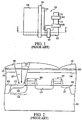
- CMOS pixel cell 100 generally comprises a photo-conversion device 120 for generating charge in response to external light incident on the pixel, and a transfer gate 106 for transferring photoelectric charges from the device 120 to a sensing node, typically a floating diffusion region 110.
- the floating diffusion region 110 is electrically connected to the gate 108 of an output source follower transistor.
- the pixel cell 100 also includes a reset transistor having a gate 107 for resetting the floating diffusion region 110 to a predetermined voltage before sensing a signal; and a row select transistor having a gate 109 for outputting a signal from the source follower transistor to an output terminal in response to a row select signal.
- a reset transistor having a gate 107 for resetting the floating diffusion region 110 to a predetermined voltage before sensing a signal
- a row select transistor having a gate 109 for outputting a signal from the source follower transistor to an output terminal in response to a row select signal.
- FIG. 2 is a diagrammatic side sectional view of the pixel cell 100 of FIG. 1 taken along line 2-2'.
- the exemplary CMOS pixel cell 100 has a pinned photodiode as the photo-conversion device 120.
- Pinned photodiode 120 is adjacent to the gate 106 of a transfer transistor and has a p-n-p construction comprising a p-type surface layer 123 and an n-type photodiode region 122 within a p-type substrate 101.
- CMOS pixel cell 100 depicted in FIGS. 1 and 2 free electrons are generated by incident light and accumulate in the n-type photodiode region 122. This photo-generated charge is transferred to the floating diffusion region 110 when gate 106 receives a signal that turns on the transfer transistor.
- the source follower transistor produces an output signal from the transferred charge in response to the voltage level received by gate 108.
- pinned photodiode 120 is exposed to external light, represented by arrows 187.
- Other portions of pixel cell 100 are shielded from light, for example, by a metal layer 186.
- Structures formed above pinned photodiode 120 are typically transparent and may include a color filter 185 and a microlens 180.
- Conventional pixel cell 100 may also include other layers formed over substrate 101 and photodiode 120, such as insulating and passivation layers (not shown).
- pixel cell 100 is capable of supporting correlated double sampling (CDS) to reduce noise and obtain a more accurate pixel signal.
- CDS correlated double sampling
- the predetermined voltage to which floating diffusion region 110 controls gate 108 to read out a pixel reset signal V rst .
- V rst a pixel reset signal
- V pc1 a pixel image signal
- the two values, V rst and V pcl are subtracted thereby reducing noise.
- 4T pixel cell 100 provides lower dark current, which also reduces noise.
- Japanese patent application no. JP58119279 (A ) relates to obtaining a correct storage time without destructive operation by providing a selective non-destructive readout element possible for sequential selection and controlling the storage time with the readout element.
- Optical charges are stored in photoelectric conversion elements, a transfer switch is closed with the input from a transfer terminal, optical information is converted into a serial signal at an analog shift register with a clock and outputted to a terminal via an amplifier.
- the clock from a terminal is counted at a counter, the count value sequentially turns on a selecting switch, the amount of optical charge is read out at a terminal with non-destruction at a FET and a resistor, and transferred just before the saturation of the maximum optical charge through the discrimination of the maximum value of the level.
- Embodiments of the invention provide pixel cells and methods of forming pixel cells that include two photo-conversion devices. Separate output signals can be read out for the two devices, making it possible to read out signals from one to determine when to read out signals from the other.
- Embodiments of the invention also provide an image sensor comprising an array of pixel cells, and pixel cells of the array. At least two pixel cells of the array each comprise a first photo-conversion device for generating charge, a second photo- conversion device for generating charge, and readout circuitry for reading out signals indicating charge generated by the first photo-conversion device and signals indicating charge generated by the photo-conversion second device. There is also circuitry for monitoring the charge generated by the second photo-conversion devices, which may or may not be part of the image sensor. According to embodiments of the invention, the charge generated by the second photo-conversion devices is monitored by sampling the voltages on the second photo-conversion devices. A time for readout of pixel cell of the array is based on the sampled voltages of the second photo-conversion devices.
- a second photo-conversion device within a pixel cell allows both automatic light control (ALC) and correlated double sampling (CDS) operations. Additionally an image sensor employing a number of pixel cells according to embodiments of the invention may perform ALC and CDS operations.
- ALC automatic light control
- CDS correlated double sampling
- a pixel cell includes at least two photo-conversion devices that can be separately read out.
- Pixel cells of the embodiments are especially useful for implementing automatic light control (ALC) in a pixel cell with more than three transistors, such as a four transistor (4T) pixel cell, which includes a transfer gate between a first photo-conversion device and a floating diffusion region.
- ALC automatic light control
- 4T four transistor
- the first photo-conversion device is not directly connected to the gate of the source follower transistor, it is not possible to read out photo-generated charge on the first device without altering charge stored by the first photo-conversion device, such as pinned photodiode 120 in FIGS. 1 and 2 .
- 4T, and other similarly configured pixel cells make it possible to perform correlated double sampling (CDS), they also may interfere with ALC.
- FIG. 3 is a top plan view of a CMOS pixel cell 300 according to an exemplary embodiment of the invention.
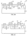
- FIGS. 4A-4C depict cross-sectional views of pixel cell 300 along line 4-4' according to exemplary embodiments of the invention.
- FIG. 5 is a schematic diagram of pixel cell 300.
- Pixel cell 300 includes a first photo-conversion device, shown as a pinned photodiode 320, for generating charge in response to external light incident on pixel cell 300.
- a first photo-conversion device shown as a pinned photodiode 320
- Adjacent to pinned photodiode 320 is a gate 306 of a first transistor.
- the first transistor is illustratively a transfer transistor for transferring photo-generated charge to a sensing node at a time for readout of the photo-generated charge.
- the sensing node is configured to include a second photo-conversion device, and is illustratively a floating diffusion region 330.
- Floating diffusion region 330 has an area, A 330 , which is enlarged as compared to a floating diffusion region of a conventional pixel cell. Area A 330 is sufficiently large to allow floating diffusion region 330 to function as a second photo-conversion device. As floating diffusion region 330 generates charge, the voltage level of floating diffusion region 330 can be monitored.
- pixel cell 300 may support automatic light control (ALC) operations as well as correlated double sampling (CDS), as described in more detail herein.
- ALC automatic light control
- CDS correlated double sampling
- Pixel cell 300 also includes gates 307, 308, and 309 of reset, source follower and row select transistors, respectively, and source/drain regions 315 of those transistors.
- a substrate 301 which may be a p-type substrate.
- isolation regions in the substrate 301 which are shown as shallow trench isolation (STI) regions 302.
- STI shallow trench isolation
- Adjacent to an STI region 302 is pinned photodiode 320.
- Pinned photodiode 320 includes a charge accumulation region 321 below the surface of the substrate 301, which is illustratively an n-type region.
- Over charge accumulation region 321 is a p+ surface layer 323.
- Adjacent to pinned photodiode 320 is transfer gate 306.
- floating diffusion region 330 may be an n-type region below the surface of substrate 301.
- floating diffusion region 330 may be a second pinned photodiode 335 and include an n-type region 331 below the surface of the substrate and underlying a p+ surface layer 333.
- second pinned photodiode 335 may have a higher pinning voltage, V pin2 , than a pinning voltage, V pin1 , for pinned photodiode 320.
- a second photo-conversion device of pixel cell 300 is primarily referred to herein as a floating diffusion region 330. It should be understood that a reference to floating diffusion region 330 is also a reference to a second photo-conversion device, and more specifically to second pinned photodiode 335, except where differences between such devices are explicitly addressed herein.
- floating diffusion region 330 functions as a second photo-conversion device. Therefore, it is not completely shielded from light, for example, by a metal layer, as in conventional pixel cell 100 ( FIGS. 1 and 2 ). Although no metal layer is shown in FIG. 4A , it should be noted that a metal layer may shield other portions of the pixel cell 300. As shown in FIG. 4A , light, represented by arrows 387, may reach floating diffusion region 330 through components of pixel cell 300 formed over substrate 301, such as, for example, a microlens 380 and a color filter 385.
- pixel cell 300 There may also be additional layers (not shown) of pixel cell 300 over substrate 301, including, but not limited to insulating and passivation layers, which allow light to reach floating diffusion region 330.
- additional layers including, but not limited to insulating and passivation layers, which allow light to reach floating diffusion region 330.
- insulating and passivation layers allow light to reach floating diffusion region 330.
- light access is only shown in FIG. 4A , however, light is similarly able to reach floating diffusion region 330, or second pinned photodiode 335, in the embodiments of FIGS. 4B and 4C , respectively.
- Floating diffusion region 330 is adjacent to the gate 307 of a reset transistor, which has a source/drain region 315 on a side of the reset gate 307 opposite to floating diffusion region 330.
- a dielectric layer 342 which is illustratively over pinned photodiode 320, transfer gate 306 and floating diffusion region 330; partially over reset gate 307 on a side adjacent to floating diffusion region 330; and in a spacer on a sidewall of reset gate 307.
- FIGS. 4A and 4C show p-well 303 extending from a surface of substrate 301 to a depth below the surface, and extending under reset gate 307, an STI region 302 adjacent to the reset source/drain region 315, and a portion of transfer gate 306.
- Floating diffusion region 330 or second pinned photodiode 335 ( FIG. 4C )
- reset source/drain region 315 are in p-well 303.
- pixel cell 300 may include two or more p-well regions, such as regions 304a, 304b, as shown in FIG. 4B .
- p-well 304a below the transfer gate 306, extending from a surface of substrate 301 to a depth below the surface.
- p-well 304b extending from a surface of substrate 301 to a depth below the surface, and extending under an STI region 302 adjacent to the reset source/drain region 315, and a portion of the reset gate 307.
- the reset source/drain region 315 is formed in p-well 304b.
- Floating diffusion region 330 is not formed within a p-well, and, thus, may have an improved response to red light.
- P-wells 304a, 304b may also be used in place of p-well 303 in the embodiment of FIG. 4C , such that second photodiode 335 is not formed in a p-well.
- the invention may also be embodied in other pixel cell designs, including those designs having different numbers of transistors. Without being limiting, such a design may include a five-transistor (5T) pixel cell or a six-transistor (6T) pixel cell. Five and six-transistor pixel cells differ from a 4T pixel cell by the addition of one or more transistors, such as a shutter transistor and/or an antiblooming transistor. Additionally, the invention is not limited to pixel cells having a gate of a source follower transistor connected to a second photo-conversion device. Accordingly, alternative readout circuitry may be employed within a pixel cell.
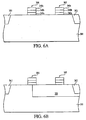
- FIGS. 6A through 6H An exemplary embodiment for the fabrication of pixel cell 300 is described below with reference to FIGS. 6A through 6H . No particular order is required for any of the actions described herein, except for those logically requiring the results of prior actions. Accordingly, while the actions below are described as being performed in a general order, the order is exemplary only and may be altered.
- FIG. 6A illustrates a pixel cell 300 at an initial stage of fabrication.
- Substrate 301 is illustratively of a first conductivity type, which is illustratively p-type.
- Isolation regions 302 are formed in the substrate 301 and filled with a dielectric material.
- the dielectric material may be an oxide material, for example a silicon oxide, such as SiO or SiO 2 ; oxynitride; a nitride material, such as silicon nitride; silicon carbide; a high temperature polymer; or other suitable dielectric material.
- the isolation region 302 can be a shallow trench isolation (STI) region and the dielectric material is preferably a high density plasma (HDP) oxide, a material which has a high ability to effectively fill narrow trenches.
- STI shallow trench isolation
- HDP high density plasma
- a first insulating layer 340a of, for example, silicon oxide is grown or deposited on the substrate 301.
- First insulating layer 340a serves as the gate oxide layer for the subsequently formed transistor gates 306 and 307.
- a layer of conductive material 340b is deposited over the oxide layer 340a.
- the conductive layer 340b serves as the gate electrode for the subsequently formed transistors.
- Conductive layer 340b may be a layer of polysilicon, which may be doped to a second conductivity type, e.g. n-type.
- a second insulating layer 340c is deposited over the polysilicon layer 340b.
- Second insulating layer 340c may be formed of, for example, an oxide (SiO 2 ), a nitride (silicon nitride), an oxynitride (silicon oxynitride), ON (oxide-nitride), NO (nitride-oxide), or ONO (oxide-nitride-oxide).
- the layers, 340a, 340b, and 340c may be formed by conventional deposition methods, such as chemical vapor deposition (CVD) or plasma chemical vapor deposition (PECVD), among others.
- CVD chemical vapor deposition
- PECVD plasma chemical vapor deposition
- the layers 340a, 340b, and 340c are then patterned and etched to form the multilayer gate stack structures 306 and 307 shown in FIG. 6A .
- the gate stack 306 is the gate structure for a transfer transistor and gate stack 307 is the gate structure for a reset transistor.
- the invention is not limited to the structure of the gates 306 and 307 described above. Additional layers may be added or the gates 306 and 307 may be altered as is desired and known in the art.
- a silicide layer (not shown) may be formed between the gate electrodes 340b and the second insulating layers 340c.
- the silicide layer may be included in the gates 306 and 307, or in all of the transistor gate structures in an image sensor circuit, and may be titanium silicide, tungsten silicide, cobalt silicide, molybdenum silicide, or tantalum silicide.
- This additional conductive layer may also be a barrier layer/refractor metal, such as TiN/W or W/N x /W, or it could be formed entirely of WN x .
- a well of a first conductivity type illustratively a p-well 303, is implanted into substrate 301 as shown in FIG. 6B .
- P-well 303 is formed in the substrate 301 from a point below the transfer gate 306 to a point below the STI region 302 that is on a side of the reset gate 307 opposite to the transfer gate 306.
- FIG. 6B A well of a first conductivity type, illustratively a p-well 303, is implanted into substrate 301 as shown in FIG. 6B .
- P-well 303 is formed in the substrate 301 from a point below the transfer gate 306 to a point below the STI region 302 that is on a side of the reset gate 307 opposite to the transfer gate 306.
- a p-type dopant such as boron
- the p-wells 303, 304a, 304b are formed having a p-type dopant concentration that is higher than adjacent portions of the substrate 301.
- a doped region 321 of a second conductivity type is implanted in the substrate 301 for the pinned photodiode 320, as shown in FIG. 6D .
- Doped region 321 is illustratively lightly doped n-type region.
- Doped region 321 may be formed by methods known in the art. For example, a layer of photoresist (not shown) may be patterned over the substrate 301 having an opening over the surface of the substrate 301 where pinned photodiode 320 is to be formed.
- An n-type dopant such as phosphorus, arsenic, or antimony, may be implanted through the opening and into the substrate 301. Multiple implants may be used to tailor the profile of region 321. If desired, an angled implantation may be conducted to form the doped region 321, such that implantation is carried out at angles other than 90 degrees relative to the surface of the substrate 301.
- Pinned photodiode region 321 is on an opposite side of the transfer gate 306 from the reset gate 307 and is approximately aligned with an edge of the transfer gate 306 forming a photosensitive charge accumulating region for collecting photo-generated charge.
- a floating diffusion region 330 is formed between transfer gate 306 and reset gate 307.
- Floating diffusion region 330 may be formed by known methods as a doped region of a second conductivity type, which is illustratively n-type, in the substrate 301.
- floating diffusion region is formed having a surface area, such that floating diffusion region 330 serves as a second photo-conversion device for generating and accumulating charge in response to external incident light.
- floating diffusion region 330 may instead be a second pinned photodiode 335, which may be formed as described in connection with FIGS. 6D and 6G .
- second pinned photodiode 335 may be formed at a same time and in a same manner as pinned photodiode 320.
- FIG. 6F depicts the formation of an oxide layer 342.
- layer 342 is an oxide layer, but layer 342 may instead be any appropriate dielectric material, such as silicon dioxide, silicon nitride, an oxynitride, ON, NO, ONO, or TEOS, among others, formed by methods known in the art.
- Doped surface layer 323 for the pinned photodiode 320 is implanted, as illustrated in FIG. 6G .
- Doped surface layer 323 is doped to a first conductivity type, which for exemplary purposes is p-type.
- doped surface layer 323 is a highly doped p+ surface layer.
- a p-type dopant, such as boron, indium, or any other suitable p-type dopant, may be used to form p+ surface layer 323.
- P+ surface layer 323 may be formed by known techniques. For example, layer 323 may be formed by implanting p-type ions through openings in a layer of photoresist. Alternatively, layer 323 may be formed by a gas source plasma doping process, or by diffusing a p-type dopant into the substrate 301 from an in-situ doped layer or a doped oxide layer deposited over the area where layer 323 is to be formed.
- Oxide layer 342 may be etched such that remaining portions form a sidewall spacer on a sidewall of reset gate 307 opposite to floating diffusion region 330 and a protective layer 342 over the transfer gate 306, the photodiode 320, the floating diffusion region 330 and a portion of the reset gate 307 adjacent to the floating diffusion region 330.
- oxide layer 342 may be etched such that only sidewall spacers on gates 306 and 307 remain.
- Reset source/drain region 315 may be implanted by known methods to achieve the structure shown in FIG. 6H .
- Source/drain region 315 is formed as a region of a second conductivity type, which for exemplary purposes is n-type. Any suitable n-type dopant, such as phosphorus, arsenic, or antimony, may be used to form source/drain region 315.
- Conventional processing methods may be used to complete the pixel cell 300. For example, insulating, shielding, and metallization layers to connect gate lines and other connections to the pixel cell 300 may be formed. As noted above, floating diffusion region 330 serves as a second photo-conversion device and, therefore, is not completely shielded from light by structures of pixel cell 300. Also, the entire surface may be covered with a passivation layer (not shown) of, for example, silicon dioxide, BSG, PSG, or BPSG, which is CMP planarized and etched to provide contact holes, which are then metallized to provide contacts. Conventional layers of conductors and insulators may also be used to interconnect the structures and to connect pixel cell 300 to peripheral circuitry, and filters 385 and microlenses 380 ( FIG. 4A ) may also be formed.
- the invention is not limited to these embodiments.
- the invention also has applicability to other types of photo-conversion devices, such as a photodiode formed from np or npn regions in a substrate, a photogate, or a photoconductor. If an npn-type photodiode is formed the dopant and conductivity types of all structures would change accordingly, with the transfer and shutter gates being part of PMOS transistors, rather than NMOS transistors as in the embodiments described above.
- pixel cell 300 may be part of an array 777 of pixel cells. Pixel cells of array 777 are illustratively arranged in columns and rows. In the example of FIG. 7 , pixel cell 300 is shown as part of row x and column y. Array 777 may have any number of columns and rows. For simplicity, only rows R x , R n , and R w ; and columns C y , C z , and Cq are explicitly depicted. Values for x, w, n, y, z, and q may be chosen as desired and may depend on the total number of columns and rows for a particular array.
- All pixel cells in rows R x , R n , and R w may be formed as described above in connection with FIGS. 6A-6H .
- three non-adjacent rows of pixel cells 300 are shown in FIG. 7 , the invention is not limited to a specific number of rows of pixel cells 300, or a specific configuration of such rows. Accordingly, rows of pixel cells 300 may be adjacent to one another; and any number of rows of array 777 may include, or all pixel cells of array may be pixel cells 300.
- FIG. 8 is a block diagram of an exemplary CMOS image sensor 888 according to an embodiment of the invention.
- the image sensor includes pixel array 777 described above in connection with FIG. 7 .
- the image sensor 888 also includes row select lines, and column select lines for selecting rows and columns of array 777 for readout or monitoring.
- the row lines are selectively activated by a row driver 891 in response to row address decoder 892.
- the column select lines are selectively activated by a column driver 893 in response to column address decoder 897.
- the pixel array 777 is operated by the timing and control circuit 895, which controls address decoders 892, 897 for selecting the appropriate row and column lines for pixel signal readout or monitoring.
- the pixel signals are read by a sample and hold circuit (S/H) 896 associated with the column driver 893, which includes one S/H cell for storing a pixel image signal (V pc1 ) and another S/H cell for storing a pixel signal corresponding to charge generated by photo-conversion in the floating diffusion region (V pc2 ).
- V pc1 is representative of the charge accumulated on photodiode 320.
- Image sensor 888 also includes ALC circuitry 883 for performing ALC operations.
- ALC circuitry 883 monitors V pc2 from pixel cells under control of timing and control circuitry 895.
- the term "monitor” means obtaining signals V pc2 until a criterion is met.
- circuitry 883 causes a readout process to commence
- ALC circuitry 883 may include a peak value (PV) monitoring circuit 885 and an average value (AV) monitoring circuit 884 selected by switch 886 in response to timing and control circuitry 895. Where a time for readout process, including readout of V pc1 , is to be determined based on a monitored pixel cell having accumulated the greatest amount of charge in its floating diffusion region 330, peak value monitoring circuit 885 is used. Circuit 885 may be configured as is known in the art. When V pc2 for any one of the monitored pixel cells is approximately equal to a reference trigger voltage, V trigger , ALC circuitry 883 causes timing and control circuitry 895 to begin a readout process, including readout of V pc1 , of all pixel cells of array 777.
- PV peak value
- AV average value
- average value monitoring circuit 884 is used.
- Circuit 884 may be configured as is known in the art.
- ALC circuitry 883 monitors signals, V pc2 , from predetermined pixel cells and determines an average value V avg of the monitored signals. When V avg is approximately equal to V trigger , ALC circuitry 883 causes timing and control circuitry 895 to begin the readout process of all pixel cells of array 777.
- ALC circuitry 883 is depicted as part of image sensor 888, ALC circuitry 883 may also be separate from image sensor 888. Without being limiting, for example, ALC circuitry may be included in the form of hardware or equivalent software in a processor, such as a CPU, which communicates with image sensor 888.
- V trigger may be selected as desired.
- V trigger may be chosen such that readout will occur only when pixel cells of array 777 have accumulated sufficient charge to result in an image in which characteristics of the imaged subject matter are visible. Otherwise stated, V trigger may be chosen such that a resultant image will not be too dark.
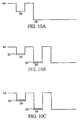
- FIGS. 9A-9C are timing diagrams for the monitoring operations of image sensor 888 according to an exemplary embodiment of the invention.
- charge accumulated by floating diffusion regions 330 of pixel cells 300 in rows R x , R n , and R w is monitored.
- monitoring operations are described with reference to a single pixel cell 300, however, all monitored pixel cells 300 of array 777 may operate as described below in connection with FIGS. 9A-9C .
- RS row select signal
- timing and control circuitry 895 pulses a sample and hold reset (SHR) signal high to cause sample and hold (S/H) circuitry 896 to read out the voltage, V pc2 , which indicates the voltage on the floating diffusion region 330.
- ALC circuitry 883 monitors V pc2 .
- V pc2 V dd .
- the reset gate is in an off state
- pinned photodiode 320 has generated an amount of charge 1070
- floating diffusion region 330 has generated an amount of charge 1071.
- the amounts of charge 1070, 1071 generated by pinned photodiode 320 and floating diffusion region 330, respectively, depend on the amount of external light incident on pixel cell 300.
- the charge 1071 on floating diffusion region 330 is monitored as illustrated in FIG. 9B in response to signals from timing and control circuit 895. When an RS signal and SHR signal are high, V pc2 is sampled, and has a magnitude that depends on charge 1071.
- peak value monitoring circuitry 885 is used and no monitored pixel cell has a V pc2 which has approximately reached a value of V trigger , monitoring continues and the charge 1070 on pinned photodiode 320 is not read out.
- average value monitoring circuitry 884 is used and V avg has not approximately reached the value of V trigger , monitoring continues and the charge 1070 on pinned photodiode 320 is not read out.
- average value monitoring circuitry 884 is used and V avg has not approximately reached the value of V trigger , so the monitoring process continues.
- V avg is approximately equal to V trigger .
- monitoring circuitry 884 provides a signal to timing and control circuitry 895, indicating that the criterion has been met for readout of the charge 1072 on pinned photodiode 320.
- timing and control circuitry 895 provides signals for readout of all pixel cells of array 777.
- FIG. 11 depicts an exemplary timing diagram for readout of the pixel cell 300.
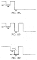
- FIGS. 12A-12C show potential well diagrams illustrating readout of the charge 1072 on pinned photodiode 320.
- a RS signal turns on the gate 309 of the row select transistor.
- a reset signal is pulsed high causing the gate 307 of the reset transistor to turn on to reset the floating diffusion region 330 to V dd .
- the reset gate When the reset gate is in an on state, there is no potential well corresponding to the floating diffusion region 330, as shown in FIG. 12A .
- the reset voltage on the floating diffusion region 330 is applied to the gate of the source follower transistor, providing current that passes through the row select transistor to readout circuitry.
- the readout circuitry connects the current to a voltage level V pc2 at the input to S/H 896.
- An SHR signal is also pulsed high to cause S/H 896 to store V pc2 .
- the reset and SHR signals transition to low.
- FIG. 12C shows the potential well diagram as photo-generated charge is transferred from pinned photodiode 320 to floating diffusion region 330.
- transfer gate 306 is in an on state, a potential barrier between pinned photodiode 320 and floating diffusion region 330 is lowered and photo-generated charge 1072 moves to floating diffusion region 330. Once the charge is transferred to floating diffusion region 330, the TX signal passes to low.
- the photo-generated charge 1072 on floating diffusion region 330 is applied to the gate 308 of the source follower transistor to control the current passing through row select transistor to readout circuitry.
- the readout circuitry connects the current to a voltage level V pc1 at the input to S/H 896.
- a sample and hold signal (SHS) signal is also pulsed high to cause S/H 896 to store V pc1 , indicating the quantity of photo-generated charge 1072 from the photodiode 320.
- SHS sample and hold signal
- V pc2 is representative of the reset voltage, V dd , on the floating diffusion region 330, and not photo-generated charge.
- the differential signal is amplified and digitized by analog to digital converter (ADC) 898.
- ADC analog to digital converter
- the analog to digital converter 898 supplies the digitized pixel signals to an image processor 889 which forms a digital image.
- a processor-based system 1313 is illustrated generally in FIG. 13 .
- a processor-based system 1313 is exemplary of a system having digital circuits that could include CMOS imager devices. Without being limiting, such a system could include a computer system, camera system, scanner, machine vision, vehicle navigation, video phone, surveillance system, auto focus system, star tracker system, motion detection system, image stabilization system, and data compression system. Notably, the processor-based system 1313 may be particularly useful in camera systems for medical devices, such as endoscopes or pill cameras.
- a processor-based system for example a computer system, generally comprises a central processing unit (CPU) 1314, such as a microprocessor, that communicates with an input/output (I/O) device 1310 over a bus 1312.
- the CMOS imager 888 which produces an image output from a pixel array, also communicates with the CPU 1314 over bus 1312.
- the processor-based system 1313 also includes random access memory (RAM) 1311, and may include peripheral devices, such as a floppy disk drive 1315 and a compact disk (CD) ROM drive 1316, which also communicate with CPU 1314 over the bus 1352.
- the CMOS imager 888 may be combined with a processor, such as a CPU, digital signal processor, or microprocessor, with or without memory storage on a single integrated circuit or on a different chip than the processor.
Landscapes
- Engineering & Computer Science (AREA)
- Multimedia (AREA)
- Signal Processing (AREA)
- Solid State Image Pick-Up Elements (AREA)
- Transforming Light Signals Into Electric Signals (AREA)
Claims (8)
- Verfahren zum Betreiben eines Bildsensors, welches Verfahren umfasst:Erzeugen einer Ladung als Reaktion auf Licht innerhalb einer Anordnung von Pixel-Zellen (300), von welchen jede vier oder mehr Transistoren (306, 307, 308, 309) hat, wobei mindestens zwei der Pixel-Zellen jeweils erste (320) und zweite (330) Photoumwandlungseinrichtungen aufweisen;Überwachen der durch die zweiten Photoumwandlungseinrichtungen erzeugten Ladung, um eine Belichtungszeit der ersten Photoumwandlungseinrichtungen zu steuern, durch:Erhalten von Signalen, die für die durch die zweiten Photoumwandlungseinrichtungen erzeugte Ladung repräsentativ sind,Anwenden eines Kriteriums auf die Signale, undFeststellen, wenn das Kriterium erfüllt ist; undAuslesen der durch die ersten Photoumwandlungseinrichtungen erzeugten Ladung, wenn das Kriterium erfüllt ist.
- Verfahren nach Anspruch 1, wobei der Vorgang des Anwendens des Kriteriums das Vergleichen der Signale mit einer Referenzspannung umfasst, und wobei der Vorgang des Feststellens, wenn das Kriterium erfüllt ist, das Feststellen, wenn irgendeines der Signale etwa gleich der Referenzspannung ist, umfasst.
- Verfahren nach Anspruch 1, wobei die Mehrzahl der Pixel-Zellen Teil einer Anordnung (777) sind, wobei die Pixel-Zellen in einer Mehrzahl von Spalten und Reihen angeordnet sind, wobei der Vorgang des Erzeugens einer Ladung das Erzeugen einer Ladung durch erste und zweite Photoumwandlungseinrichtungen innerhalb jeder Pixel-Zelle von mindestens zwei Reihen umfasst, und wobei der Vorgang des Überwachens der durch die zweiten Photoumwandlungsvorrichtungen erzeugten Ladung das Überwachen der durch die zweiten Photoumwandlungsvorrichtungen aller Pixel-Zellen in den mindestens zwei Reihen erzeugten Ladung umfasst.
- Verfahren nach Anspruch 1, wobei der Vorgang des Auslesens der durch die ersten Photoumwandlungseinrichtungen erzeugten Ladung umfasst:Zurücksetzen aller zweiten Photoumwandlungseinrichtungen auf eine vorbestimmte Spannung;Auslesen der vorbestimmten Spannung aus jeder zweiten Photoumwandlungseinrichtung;Übertragen der durch jede erste Photoumwandlungseinrichtung erzeugten Ladung auf die zweite Photoumwandlungseinrichtung innerhalb einer selben Pixel-Zelle durch Betätigen von Gattern von Transistoren; undAuslesen der durch jede erste Photoumwandlungseinrichtung erzeugten Ladung aus jeder zweiten Photoumwandlungseinrichtung.
- Bildsensor, welcher umfasst:Mittel (320, 330) zum Erzeugen einer Ladung als Reaktion auf Licht innerhalb einer Anordnung von Pixel-Zellen (300), von welchen jede vier oder mehr Transistoren (306, 307, 308, 309) hat, wobei mindestens zwei der Pixel-Zellen jeweils erste (320) und zweite (330) Photoumwandlungseinrichtungen aufweisen;Mittel (883) zum Überwachen der durch die zweiten Photoumwandlungseinrichtungen erzeugten Ladung, um eine Belichtungszeit der ersten Photoumwandlungseinrichtungen zu steuern, einschließlich:Mitteln zum Erhalten von Signalen, die für die durch die zweiten Photoumwandlungseinrichtungen erzeugte Ladung repräsentativ sind,Mitteln zum Anwenden eines Kriteriums auf die Signale, undMittel zum Feststellen, wenn das Kriterium erfüllt ist; undMittel (893, 896) zum Auslesen der durch die ersten Photoumwandlungseinrichtungen erzeugten Ladung, wenn das Kriterium erfüllt ist.
- Bildsensor nach Anspruch 5, wobei das Mittel zum Anwenden des Kriteriums angeordnet ist, um die Signale mit einer Referenzspannung zu vergleichen, und wobei das Mittel (884) zum Feststellen, wenn das Kriterium erfüllt ist, angeordnet ist, um festzustellen, wenn ein Durchschnittswert der Signale etwa gleich der Referenzspannung ist.
- Bildsensor nach Anspruch 5, wobei die Mehrzahl der Pixel-Zellen Teil einer Anordnung (777) sind, wobei die Pixel-Zellen in einer Mehrzahl von Spalten und Reihen angeordnet sind, wobei das Mittel zum Erzeugen einer Ladung angeordnet ist, um eine Ladung durch erste und zweite Photoumwandlungseinrichtungen innerhalb jeder Pixel-Zelle von mindestens zwei Reihen zu erzeugen, und wobei das Mittel zum Überwachen der durch die zweiten Photoumwandlungsvorrichtungen erzeugten Ladung angeordnet ist, um die durch die zweiten Photoumwandlungsvorrichtungen aller Pixel-Zellen in den mindestens zwei Reihen erzeugte Ladung zu überwachen.
- Bildsensor nach Anspruch 5, wobei das Mittel zum Auslesen der durch die ersten Photoumwandlungseinrichtungen erzeugten Ladung angeordnet ist zum:Zurücksetzen aller zweiten Photoumwandlungseinrichtungen auf eine vorbestimmte Spannung;Auslesen der vorbestimmten Spannung aus jeder zweiten Photoumwandlungseinrichtung;Übertragen der durch jede erste Photoumwandlungseinrichtung erzeugten Ladung auf die zweite Photoumwandlungseinrichtung innerhalb einer selben Pixel-Zelle durch Betätigen von Gattern von Transistoren; undAuslesen der durch jede erste Photoumwandlungseinrichtung erzeugten Ladung aus jeder zweiten Photoumwandlungseinrichtung.
Applications Claiming Priority (3)
| Application Number | Priority Date | Filing Date | Title |
|---|---|---|---|
| US48390603P | 2003-07-02 | 2003-07-02 | |
| US10/689,635 US7105793B2 (en) | 2003-07-02 | 2003-10-22 | CMOS pixels for ALC and CDS and methods of forming the same |
| PCT/US2004/020930 WO2005006738A1 (en) | 2003-07-02 | 2004-06-30 | Cmos imaging for automatic exposure control and correlated double sampling |
Publications (2)
| Publication Number | Publication Date |
|---|---|
| EP1649685A1 EP1649685A1 (de) | 2006-04-26 |
| EP1649685B1 true EP1649685B1 (de) | 2014-01-22 |
Family
ID=33555638
Family Applications (1)
| Application Number | Title | Priority Date | Filing Date |
|---|---|---|---|
| EP04756394.5A Expired - Lifetime EP1649685B1 (de) | 2003-07-02 | 2004-06-30 | Cmos bildaufnehmer mit automatischer integrationszeitsteuerung und doppelter korrelierter abtastung |
Country Status (6)
| Country | Link |
|---|---|
| US (3) | US7105793B2 (de) |
| EP (1) | EP1649685B1 (de) |
| JP (1) | JP2007529145A (de) |
| KR (1) | KR100762614B1 (de) |
| CN (1) | CN1843026B (de) |
| WO (1) | WO2005006738A1 (de) |
Families Citing this family (51)
| Publication number | Priority date | Publication date | Assignee | Title |
|---|---|---|---|---|
| US6879340B1 (en) * | 1998-08-19 | 2005-04-12 | Micron Technology Inc. | CMOS imager with integrated non-volatile memory |
| JP3965049B2 (ja) * | 2001-12-21 | 2007-08-22 | 浜松ホトニクス株式会社 | 撮像装置 |
| US7105793B2 (en) * | 2003-07-02 | 2006-09-12 | Micron Technology, Inc. | CMOS pixels for ALC and CDS and methods of forming the same |
| US7115855B2 (en) * | 2003-09-05 | 2006-10-03 | Micron Technology, Inc. | Image sensor having pinned floating diffusion diode |
| KR100855957B1 (ko) * | 2004-02-09 | 2008-09-02 | 삼성전자주식회사 | 화면 주변부의 밝기를 보상하는 고체 촬상 소자 및 그구동 방법 |
| US7332703B2 (en) * | 2004-03-22 | 2008-02-19 | Micron Technology, Inc. | Imaging structure including a pixel with multiple signal readout circuits and methods of operation for imaging structure |
| KR100649019B1 (ko) * | 2004-08-11 | 2006-11-24 | 동부일렉트로닉스 주식회사 | 씨모스 이미지 센서 및 그의 제조 방법 |
| US8072520B2 (en) * | 2004-08-30 | 2011-12-06 | Micron Technology, Inc. | Dual pinned diode pixel with shutter |
| JP4703163B2 (ja) * | 2004-10-19 | 2011-06-15 | 株式会社東芝 | 固体撮像装置 |
| KR100621561B1 (ko) * | 2004-11-05 | 2006-09-19 | 삼성전자주식회사 | Cmos 이미지 센서 및 그 구동 방법 |
| US7432543B2 (en) * | 2004-12-03 | 2008-10-07 | Omnivision Technologies, Inc. | Image sensor pixel having photodiode with indium pinning layer |
| US7348651B2 (en) * | 2004-12-09 | 2008-03-25 | Taiwan Semiconductor Manufacturing Co., Ltd. | Pinned photodiode fabricated with shallow trench isolation |
| JP4674894B2 (ja) * | 2004-12-28 | 2011-04-20 | パナソニック株式会社 | 固体撮像装置及びその製造方法 |
| US7551059B2 (en) * | 2005-01-06 | 2009-06-23 | Goodrich Corporation | Hybrid infrared detector array and CMOS readout integrated circuit with improved dynamic range |
| US7616231B2 (en) * | 2005-01-06 | 2009-11-10 | Goodrich Corporation | CMOS active pixel sensor with improved dynamic range and method of operation for object motion detection |
| US7518645B2 (en) * | 2005-01-06 | 2009-04-14 | Goodrich Corp. | CMOS active pixel sensor with improved dynamic range and method of operation |
| KR100674957B1 (ko) * | 2005-02-23 | 2007-01-26 | 삼성전자주식회사 | 임의의 서브-샘플링 레이트로 아날로그 신호를 평균화하여서브-샘플링하는 고체 촬상 소자 및 그 구동 방법 |
| US20070035649A1 (en) * | 2005-08-10 | 2007-02-15 | Micron Technology, Inc. | Image pixel reset through dual conversion gain gate |
| US7636115B2 (en) * | 2005-08-11 | 2009-12-22 | Aptina Imaging Corporation | High dynamic range imaging device using multiple pixel cells |
| GB2429864B (en) * | 2005-09-01 | 2008-09-24 | Micron Technology Inc | Method and apparatus providing pixel array having automatic light control pixels and image capture pixels |
| US7427734B2 (en) * | 2005-10-18 | 2008-09-23 | Digital Imaging Systems Gmbh | Multiple photosensor pixel |
| US7663165B2 (en) * | 2006-08-31 | 2010-02-16 | Aptina Imaging Corporation | Transparent-channel thin-film transistor-based pixels for high-performance image sensors |
| US20080117317A1 (en) * | 2006-11-17 | 2008-05-22 | Ray Alan Mentzer | Dim row suppression system and method for active pixel sensor arrays |
| AT504582B1 (de) * | 2006-11-23 | 2008-12-15 | Arc Austrian Res Centers Gmbh | Verfahren zur generierung eines bildes in elektronischer form, bildelement für einen bildsensor zur generierung eines bildes sowie bildsensor |
| US7675093B2 (en) * | 2006-11-28 | 2010-03-09 | Micron Technology, Inc. | Antiblooming imaging apparatus, system, and methods |
| US8184190B2 (en) * | 2006-11-28 | 2012-05-22 | Youliza, Gehts B.V. Limited Liability Company | Simultaneous global shutter and correlated double sampling read out in multiple photosensor pixels |
| US8013920B2 (en) * | 2006-12-01 | 2011-09-06 | Youliza, Gehts B.V. Limited Liability Company | Imaging system for creating an image of an object |
| KR100853793B1 (ko) * | 2006-12-29 | 2008-08-25 | 동부일렉트로닉스 주식회사 | 씨모스 이미지 센서 및 그 제조방법 |
| JP5584982B2 (ja) * | 2009-02-09 | 2014-09-10 | ソニー株式会社 | 固体撮像素子およびカメラシステム |
| US7879639B2 (en) * | 2007-04-13 | 2011-02-01 | Taiwan Semiconductor Manufacturing Company, Ltd. | Method and device to reduce dark current in image sensors |
| US8045028B1 (en) * | 2007-04-23 | 2011-10-25 | On Semiconductor Trading Ltd. | Six transistor (6T) pixel architecture |
| US7755121B2 (en) * | 2007-08-23 | 2010-07-13 | Aptina Imaging Corp. | Imagers, apparatuses and systems utilizing pixels with improved optical resolution and methods of operating the same |
| US8253810B2 (en) * | 2007-12-05 | 2012-08-28 | Aptina Imaging Corporation | Method, apparatus and system for image stabilization using a single pixel array |
| US20090224343A1 (en) * | 2008-03-06 | 2009-09-10 | Micron Technology, Inc. | Methods of forming imager devices, imager devices configured for back side illumination, and systems including the same |
| US8048708B2 (en) * | 2008-06-25 | 2011-11-01 | Micron Technology, Inc. | Method and apparatus providing an imager module with a permanent carrier |
| JP4788742B2 (ja) * | 2008-06-27 | 2011-10-05 | ソニー株式会社 | 固体撮像装置及び電子機器 |
| CN101330577B (zh) * | 2008-08-01 | 2010-04-07 | 李斌桥 | 可变换工作模式的cmos图像传感器 |
| US8319262B2 (en) * | 2009-07-31 | 2012-11-27 | Sri International | Substrate bias for CMOS imagers |
| JP2011242261A (ja) * | 2010-05-18 | 2011-12-01 | Fujifilm Corp | 放射線検出器 |
| JP2014013852A (ja) * | 2012-07-05 | 2014-01-23 | Sony Corp | リニアセンサ、撮像素子、および電子機器 |
| US9438826B2 (en) * | 2012-12-20 | 2016-09-06 | Rambus Inc. | Pixel structure and reset scheme |
| US10128296B2 (en) * | 2013-07-08 | 2018-11-13 | BAE Systems Imaging Solutions Inc. | Imaging array with improved dynamic range utilizing parasitic photodiodes |
| US9412782B2 (en) | 2013-07-08 | 2016-08-09 | BAE Systems Imaging Solutions Inc. | Imaging array with improved dynamic range utilizing parasitic photodiodes within floating diffusion nodes of pixels |
| US9319613B2 (en) * | 2013-12-05 | 2016-04-19 | Omnivision Technologies, Inc. | Image sensor having NMOS source follower with P-type doping in polysilicon gate |
| KR102426677B1 (ko) * | 2015-03-09 | 2022-07-28 | 삼성전자주식회사 | 오프셋 및 잡음이 감소되는 차분 증폭기 및 이벤트에 기반한 비전 센서 |
| JP6623594B2 (ja) * | 2015-07-22 | 2019-12-25 | セイコーエプソン株式会社 | 固体撮像素子及びその製造方法 |
| CN109479107A (zh) * | 2016-05-31 | 2019-03-15 | Bae系统成像解决方案有限公司 | 适于提供额外的颜色信息的光电检测器 |
| US10685047B1 (en) | 2016-12-08 | 2020-06-16 | Townsend Street Labs, Inc. | Request processing system |
| US10939046B2 (en) * | 2017-11-30 | 2021-03-02 | BAE Systems Imaging Solutions Inc. | LED flicker mitigation for motion pictures |
| US10250828B1 (en) * | 2017-12-21 | 2019-04-02 | SmartSens Technology (U.S.), Inc. | Global shutter image sensor with anti-blooming pixel and knee point self-calibration |
| US11064141B2 (en) * | 2019-07-24 | 2021-07-13 | Semiconductor Components Industries, Llc | Imaging systems and methods for reducing dark signal non-uniformity across pixels |
Citations (1)
| Publication number | Priority date | Publication date | Assignee | Title |
|---|---|---|---|---|
| JPH05207376A (ja) * | 1992-01-29 | 1993-08-13 | Olympus Optical Co Ltd | 固体撮像装置及びその制御方法 |
Family Cites Families (24)
| Publication number | Priority date | Publication date | Assignee | Title |
|---|---|---|---|---|
| JPS58119279A (ja) | 1982-01-07 | 1983-07-15 | Canon Inc | 蓄積型光電変換装置 |
| JP2514314B2 (ja) * | 1983-04-22 | 1996-07-10 | 旭光学工業株式会社 | 蓄積型光電変換器の蓄積時間制御方法および装置 |
| JPS6074878A (ja) * | 1983-09-30 | 1985-04-27 | Canon Inc | 光電変換器の蓄積時間補正装置 |
| JPS62230269A (ja) * | 1986-03-31 | 1987-10-08 | Toshiba Corp | 電子スチルカメラ |
| US5814803A (en) * | 1994-12-23 | 1998-09-29 | Spectra-Physics Scanning Systems, Inc. | Image reader with multi-focus lens |
| JP3031606B2 (ja) * | 1995-08-02 | 2000-04-10 | キヤノン株式会社 | 固体撮像装置と画像撮像装置 |
| JP4356121B2 (ja) | 1998-03-18 | 2009-11-04 | ソニー株式会社 | 固体撮像素子およびその駆動方法、並びにカメラシステム |
| US6459077B1 (en) * | 1998-09-15 | 2002-10-01 | Dalsa, Inc. | Bucket brigade TDI photodiode sensor |
| US6140630A (en) | 1998-10-14 | 2000-10-31 | Micron Technology, Inc. | Vcc pump for CMOS imagers |
| WO2000078034A2 (en) | 1999-06-15 | 2000-12-21 | Photobit Corporation | Dual sensitivity image sensor |
| US6376868B1 (en) | 1999-06-15 | 2002-04-23 | Micron Technology, Inc. | Multi-layered gate for a CMOS imager |
| US6310366B1 (en) | 1999-06-16 | 2001-10-30 | Micron Technology, Inc. | Retrograde well structure for a CMOS imager |
| US6326652B1 (en) | 1999-06-18 | 2001-12-04 | Micron Technology, Inc., | CMOS imager with a self-aligned buried contact |
| US6204524B1 (en) | 1999-07-14 | 2001-03-20 | Micron Technology, Inc. | CMOS imager with storage capacitor |
| US6333205B1 (en) | 1999-08-16 | 2001-12-25 | Micron Technology, Inc. | CMOS imager with selectively silicided gates |
| US6710804B1 (en) * | 2000-01-18 | 2004-03-23 | Eastman Kodak Company | CMOS active pixel image sensor with extended dynamic range and sensitivity |
| US6407440B1 (en) * | 2000-02-25 | 2002-06-18 | Micron Technology Inc. | Pixel cell with high storage capacitance for a CMOS imager |
| JP3658278B2 (ja) * | 2000-05-16 | 2005-06-08 | キヤノン株式会社 | 固体撮像装置およびそれを用いた固体撮像システム |
| US6759641B1 (en) * | 2000-09-27 | 2004-07-06 | Rockwell Scientific Licensing, Llc | Imager with adjustable resolution |
| JP4204210B2 (ja) * | 2001-08-29 | 2009-01-07 | 株式会社リコー | Pll回路 |
| US6777661B2 (en) * | 2002-03-15 | 2004-08-17 | Eastman Kodak Company | Interlined charge-coupled device having an extended dynamic range |
| US7105793B2 (en) * | 2003-07-02 | 2006-09-12 | Micron Technology, Inc. | CMOS pixels for ALC and CDS and methods of forming the same |
| US7115855B2 (en) * | 2003-09-05 | 2006-10-03 | Micron Technology, Inc. | Image sensor having pinned floating diffusion diode |
| US7238977B2 (en) * | 2004-08-19 | 2007-07-03 | Micron Technology, Inc. | Wide dynamic range sensor having a pinned diode with multiple pinned voltages |
-
2003
- 2003-10-22 US US10/689,635 patent/US7105793B2/en not_active Expired - Lifetime
-
2004
- 2004-06-30 WO PCT/US2004/020930 patent/WO2005006738A1/en not_active Ceased
- 2004-06-30 KR KR1020067000092A patent/KR100762614B1/ko not_active Expired - Fee Related
- 2004-06-30 JP JP2006518722A patent/JP2007529145A/ja active Pending
- 2004-06-30 EP EP04756394.5A patent/EP1649685B1/de not_active Expired - Lifetime
- 2004-06-30 CN CN2004800246148A patent/CN1843026B/zh not_active Expired - Fee Related
-
2005
- 2005-11-14 US US11/272,090 patent/US7312431B2/en not_active Expired - Lifetime
-
2006
- 2006-05-30 US US11/442,136 patent/US7642497B2/en not_active Expired - Lifetime
Patent Citations (1)
| Publication number | Priority date | Publication date | Assignee | Title |
|---|---|---|---|---|
| JPH05207376A (ja) * | 1992-01-29 | 1993-08-13 | Olympus Optical Co Ltd | 固体撮像装置及びその制御方法 |
Also Published As
| Publication number | Publication date |
|---|---|
| US7105793B2 (en) | 2006-09-12 |
| EP1649685A1 (de) | 2006-04-26 |
| US20070029469A1 (en) | 2007-02-08 |
| US20060060753A1 (en) | 2006-03-23 |
| CN1843026B (zh) | 2010-12-22 |
| KR100762614B1 (ko) | 2007-10-01 |
| US7312431B2 (en) | 2007-12-25 |
| JP2007529145A (ja) | 2007-10-18 |
| KR20060030890A (ko) | 2006-04-11 |
| CN1843026A (zh) | 2006-10-04 |
| US20050001143A1 (en) | 2005-01-06 |
| WO2005006738A1 (en) | 2005-01-20 |
| US7642497B2 (en) | 2010-01-05 |
Similar Documents
| Publication | Publication Date | Title |
|---|---|---|
| EP1649685B1 (de) | Cmos bildaufnehmer mit automatischer integrationszeitsteuerung und doppelter korrelierter abtastung | |
| US7115923B2 (en) | Imaging with gate controlled charge storage | |
| US7405101B2 (en) | CMOS imager with selectively silicided gate | |
| US6310366B1 (en) | Retrograde well structure for a CMOS imager | |
| US7002231B2 (en) | Barrier regions for image sensors | |
| US20070200181A1 (en) | Buried conductor for imagers | |
| JP2009506547A (ja) | 撮像装置での垂直方向ブルーミング防止制御およびクロストーク軽減のためのBtFried添加領域 | |
| JP2009534836A (ja) | ブルーミングおよびクロストークからのダーク基準列とダーク基準行の保護を改良するnウェル障壁画素 |
Legal Events
| Date | Code | Title | Description |
|---|---|---|---|
| PUAI | Public reference made under article 153(3) epc to a published international application that has entered the european phase |
Free format text: ORIGINAL CODE: 0009012 |
|
| 17P | Request for examination filed |
Effective date: 20060202 |
|
| AK | Designated contracting states |
Kind code of ref document: A1 Designated state(s): AT BE BG CH CY CZ DE DK EE ES FI FR GB GR HU IE IT LI LU MC NL PL PT RO SE SI SK TR |
|
| DAX | Request for extension of the european patent (deleted) | ||
| RAP1 | Party data changed (applicant data changed or rights of an application transferred) |
Owner name: APTINA IMAGING CORPORATION |
|
| 17Q | First examination report despatched |
Effective date: 20110928 |
|
| REG | Reference to a national code |
Ref country code: DE Ref legal event code: R079 Ref document number: 602004044320 Country of ref document: DE Free format text: PREVIOUS MAIN CLASS: H04N0003150000 Ipc: H01L0027140000 |
|
| GRAP | Despatch of communication of intention to grant a patent |
Free format text: ORIGINAL CODE: EPIDOSNIGR1 |
|
| RIC1 | Information provided on ipc code assigned before grant |
Ipc: H01L 27/14 20060101AFI20130802BHEP |
|
| INTG | Intention to grant announced |
Effective date: 20130906 |
|
| GRAS | Grant fee paid |
Free format text: ORIGINAL CODE: EPIDOSNIGR3 |
|
| GRAA | (expected) grant |
Free format text: ORIGINAL CODE: 0009210 |
|
| AK | Designated contracting states |
Kind code of ref document: B1 Designated state(s): AT BE BG CH CY CZ DE DK EE ES FI FR GB GR HU IE IT LI LU MC NL PL PT RO SE SI SK TR |
|
| REG | Reference to a national code |
Ref country code: GB Ref legal event code: FG4D |
|
| REG | Reference to a national code |
Ref country code: CH Ref legal event code: EP |
|
| REG | Reference to a national code |
Ref country code: AT Ref legal event code: REF Ref document number: 651131 Country of ref document: AT Kind code of ref document: T Effective date: 20140215 |
|
| REG | Reference to a national code |
Ref country code: IE Ref legal event code: FG4D |
|
| REG | Reference to a national code |
Ref country code: DE Ref legal event code: R096 Ref document number: 602004044320 Country of ref document: DE Effective date: 20140306 |
|
| REG | Reference to a national code |
Ref country code: SE Ref legal event code: TRGR |
|
| REG | Reference to a national code |
Ref country code: NL Ref legal event code: VDEP Effective date: 20140122 |
|
| REG | Reference to a national code |
Ref country code: AT Ref legal event code: MK05 Ref document number: 651131 Country of ref document: AT Kind code of ref document: T Effective date: 20140122 |
|
| PG25 | Lapsed in a contracting state [announced via postgrant information from national office to epo] |
Ref country code: ES Free format text: LAPSE BECAUSE OF FAILURE TO SUBMIT A TRANSLATION OF THE DESCRIPTION OR TO PAY THE FEE WITHIN THE PRESCRIBED TIME-LIMIT Effective date: 20140122 Ref country code: NL Free format text: LAPSE BECAUSE OF FAILURE TO SUBMIT A TRANSLATION OF THE DESCRIPTION OR TO PAY THE FEE WITHIN THE PRESCRIBED TIME-LIMIT Effective date: 20140122 Ref country code: AT Free format text: LAPSE BECAUSE OF FAILURE TO SUBMIT A TRANSLATION OF THE DESCRIPTION OR TO PAY THE FEE WITHIN THE PRESCRIBED TIME-LIMIT Effective date: 20140122 Ref country code: CY Free format text: LAPSE BECAUSE OF FAILURE TO SUBMIT A TRANSLATION OF THE DESCRIPTION OR TO PAY THE FEE WITHIN THE PRESCRIBED TIME-LIMIT Effective date: 20140122 Ref country code: PT Free format text: LAPSE BECAUSE OF FAILURE TO SUBMIT A TRANSLATION OF THE DESCRIPTION OR TO PAY THE FEE WITHIN THE PRESCRIBED TIME-LIMIT Effective date: 20140522 |
|
| PG25 | Lapsed in a contracting state [announced via postgrant information from national office to epo] |
Ref country code: BE Free format text: LAPSE BECAUSE OF FAILURE TO SUBMIT A TRANSLATION OF THE DESCRIPTION OR TO PAY THE FEE WITHIN THE PRESCRIBED TIME-LIMIT Effective date: 20140122 |
|
| REG | Reference to a national code |
Ref country code: DE Ref legal event code: R097 Ref document number: 602004044320 Country of ref document: DE |
|
| PG25 | Lapsed in a contracting state [announced via postgrant information from national office to epo] |
Ref country code: DK Free format text: LAPSE BECAUSE OF FAILURE TO SUBMIT A TRANSLATION OF THE DESCRIPTION OR TO PAY THE FEE WITHIN THE PRESCRIBED TIME-LIMIT Effective date: 20140122 Ref country code: EE Free format text: LAPSE BECAUSE OF FAILURE TO SUBMIT A TRANSLATION OF THE DESCRIPTION OR TO PAY THE FEE WITHIN THE PRESCRIBED TIME-LIMIT Effective date: 20140122 Ref country code: RO Free format text: LAPSE BECAUSE OF FAILURE TO SUBMIT A TRANSLATION OF THE DESCRIPTION OR TO PAY THE FEE WITHIN THE PRESCRIBED TIME-LIMIT Effective date: 20140122 Ref country code: CZ Free format text: LAPSE BECAUSE OF FAILURE TO SUBMIT A TRANSLATION OF THE DESCRIPTION OR TO PAY THE FEE WITHIN THE PRESCRIBED TIME-LIMIT Effective date: 20140122 |
|
| PG25 | Lapsed in a contracting state [announced via postgrant information from national office to epo] |
Ref country code: SK Free format text: LAPSE BECAUSE OF FAILURE TO SUBMIT A TRANSLATION OF THE DESCRIPTION OR TO PAY THE FEE WITHIN THE PRESCRIBED TIME-LIMIT Effective date: 20140122 Ref country code: PL Free format text: LAPSE BECAUSE OF FAILURE TO SUBMIT A TRANSLATION OF THE DESCRIPTION OR TO PAY THE FEE WITHIN THE PRESCRIBED TIME-LIMIT Effective date: 20140122 |
|
| PLBE | No opposition filed within time limit |
Free format text: ORIGINAL CODE: 0009261 |
|
| STAA | Information on the status of an ep patent application or granted ep patent |
Free format text: STATUS: NO OPPOSITION FILED WITHIN TIME LIMIT |
|
| 26N | No opposition filed |
Effective date: 20141023 |
|
| PG25 | Lapsed in a contracting state [announced via postgrant information from national office to epo] |
Ref country code: MC Free format text: LAPSE BECAUSE OF FAILURE TO SUBMIT A TRANSLATION OF THE DESCRIPTION OR TO PAY THE FEE WITHIN THE PRESCRIBED TIME-LIMIT Effective date: 20140122 Ref country code: LU Free format text: LAPSE BECAUSE OF FAILURE TO SUBMIT A TRANSLATION OF THE DESCRIPTION OR TO PAY THE FEE WITHIN THE PRESCRIBED TIME-LIMIT Effective date: 20140630 |
|
| REG | Reference to a national code |
Ref country code: CH Ref legal event code: PL |
|
| REG | Reference to a national code |
Ref country code: DE Ref legal event code: R097 Ref document number: 602004044320 Country of ref document: DE Effective date: 20141023 |
|
| REG | Reference to a national code |
Ref country code: IE Ref legal event code: MM4A |
|
| PG25 | Lapsed in a contracting state [announced via postgrant information from national office to epo] |
Ref country code: IE Free format text: LAPSE BECAUSE OF NON-PAYMENT OF DUE FEES Effective date: 20140630 Ref country code: CH Free format text: LAPSE BECAUSE OF NON-PAYMENT OF DUE FEES Effective date: 20140630 Ref country code: LI Free format text: LAPSE BECAUSE OF NON-PAYMENT OF DUE FEES Effective date: 20140630 |
|
| PG25 | Lapsed in a contracting state [announced via postgrant information from national office to epo] |
Ref country code: SI Free format text: LAPSE BECAUSE OF FAILURE TO SUBMIT A TRANSLATION OF THE DESCRIPTION OR TO PAY THE FEE WITHIN THE PRESCRIBED TIME-LIMIT Effective date: 20140122 |
|
| PG25 | Lapsed in a contracting state [announced via postgrant information from national office to epo] |
Ref country code: BG Free format text: LAPSE BECAUSE OF FAILURE TO SUBMIT A TRANSLATION OF THE DESCRIPTION OR TO PAY THE FEE WITHIN THE PRESCRIBED TIME-LIMIT Effective date: 20140122 |
|
| REG | Reference to a national code |
Ref country code: FR Ref legal event code: PLFP Year of fee payment: 13 |
|
| PG25 | Lapsed in a contracting state [announced via postgrant information from national office to epo] |
Ref country code: GR Free format text: LAPSE BECAUSE OF FAILURE TO SUBMIT A TRANSLATION OF THE DESCRIPTION OR TO PAY THE FEE WITHIN THE PRESCRIBED TIME-LIMIT Effective date: 20140423 |
|
| PG25 | Lapsed in a contracting state [announced via postgrant information from national office to epo] |
Ref country code: HU Free format text: LAPSE BECAUSE OF FAILURE TO SUBMIT A TRANSLATION OF THE DESCRIPTION OR TO PAY THE FEE WITHIN THE PRESCRIBED TIME-LIMIT; INVALID AB INITIO Effective date: 20040630 Ref country code: TR Free format text: LAPSE BECAUSE OF FAILURE TO SUBMIT A TRANSLATION OF THE DESCRIPTION OR TO PAY THE FEE WITHIN THE PRESCRIBED TIME-LIMIT Effective date: 20140122 |
|
| REG | Reference to a national code |
Ref country code: FR Ref legal event code: PLFP Year of fee payment: 14 |
|
| REG | Reference to a national code |
Ref country code: DE Ref legal event code: R082 Ref document number: 602004044320 Country of ref document: DE Representative=s name: BRINKMANN & PARTNER PATENTANWAELTE PARTNERSCHA, DE Ref country code: DE Ref legal event code: R082 Ref document number: 602004044320 Country of ref document: DE Representative=s name: RAUSCH WANISCHECK-BERGMANN BRINKMANN PARTNERSC, DE |
|
| REG | Reference to a national code |
Ref country code: FR Ref legal event code: PLFP Year of fee payment: 15 |
|
| PGFP | Annual fee paid to national office [announced via postgrant information from national office to epo] |
Ref country code: SE Payment date: 20220519 Year of fee payment: 19 Ref country code: IT Payment date: 20220518 Year of fee payment: 19 Ref country code: GB Payment date: 20220520 Year of fee payment: 19 Ref country code: FR Payment date: 20220519 Year of fee payment: 19 Ref country code: DE Payment date: 20220518 Year of fee payment: 19 |
|
| PGFP | Annual fee paid to national office [announced via postgrant information from national office to epo] |
Ref country code: FI Payment date: 20220524 Year of fee payment: 19 |
|
| REG | Reference to a national code |
Ref country code: DE Ref legal event code: R119 Ref document number: 602004044320 Country of ref document: DE |
|
| PG25 | Lapsed in a contracting state [announced via postgrant information from national office to epo] |
Ref country code: FI Free format text: LAPSE BECAUSE OF NON-PAYMENT OF DUE FEES Effective date: 20230630 |
|
| GBPC | Gb: european patent ceased through non-payment of renewal fee |
Effective date: 20230630 |
|
| REG | Reference to a national code |
Ref country code: SE Ref legal event code: EUG |
|
| PG25 | Lapsed in a contracting state [announced via postgrant information from national office to epo] |
Ref country code: DE Free format text: LAPSE BECAUSE OF NON-PAYMENT OF DUE FEES Effective date: 20240103 Ref country code: GB Free format text: LAPSE BECAUSE OF NON-PAYMENT OF DUE FEES Effective date: 20230630 |
|
| PG25 | Lapsed in a contracting state [announced via postgrant information from national office to epo] |
Ref country code: SE Free format text: LAPSE BECAUSE OF NON-PAYMENT OF DUE FEES Effective date: 20230701 Ref country code: FR Free format text: LAPSE BECAUSE OF NON-PAYMENT OF DUE FEES Effective date: 20230630 |
|
| PG25 | Lapsed in a contracting state [announced via postgrant information from national office to epo] |
Ref country code: IT Free format text: LAPSE BECAUSE OF NON-PAYMENT OF DUE FEES Effective date: 20230630 |