EP1636951B1 - System und verfahren zur formatierung von daten - Google Patents
System und verfahren zur formatierung von daten Download PDFInfo
- Publication number
- EP1636951B1 EP1636951B1 EP04753995A EP04753995A EP1636951B1 EP 1636951 B1 EP1636951 B1 EP 1636951B1 EP 04753995 A EP04753995 A EP 04753995A EP 04753995 A EP04753995 A EP 04753995A EP 1636951 B1 EP1636951 B1 EP 1636951B1
- Authority
- EP
- European Patent Office
- Prior art keywords
- data
- format
- output
- memory array
- stream
- Prior art date
- Legal status (The legal status is an assumption and is not a legal conclusion. Google has not performed a legal analysis and makes no representation as to the accuracy of the status listed.)
- Expired - Lifetime
Links
- 238000000034 method Methods 0.000 title claims abstract description 15
- 230000001360 synchronised effect Effects 0.000 claims description 6
- 238000004891 communication Methods 0.000 abstract description 12
- 238000006243 chemical reaction Methods 0.000 abstract description 2
- 238000003491 array Methods 0.000 description 19
- 238000013461 design Methods 0.000 description 3
- 238000012545 processing Methods 0.000 description 3
- 230000005540 biological transmission Effects 0.000 description 2
- 230000006870 function Effects 0.000 description 2
- 238000012986 modification Methods 0.000 description 2
- 230000004048 modification Effects 0.000 description 2
- 230000003416 augmentation Effects 0.000 description 1
- 230000003190 augmentative effect Effects 0.000 description 1
- 238000010586 diagram Methods 0.000 description 1
- 239000011159 matrix material Substances 0.000 description 1
Images


Classifications
-
- H—ELECTRICITY
- H04—ELECTRIC COMMUNICATION TECHNIQUE
- H04L—TRANSMISSION OF DIGITAL INFORMATION, e.g. TELEGRAPHIC COMMUNICATION
- H04L12/00—Data switching networks
- H04L12/54—Store-and-forward switching systems
- H04L12/56—Packet switching systems
- H04L12/5601—Transfer mode dependent, e.g. ATM
-
- H—ELECTRICITY
- H04—ELECTRIC COMMUNICATION TECHNIQUE
- H04L—TRANSMISSION OF DIGITAL INFORMATION, e.g. TELEGRAPHIC COMMUNICATION
- H04L12/00—Data switching networks
- H04L12/54—Store-and-forward switching systems
- H04L12/56—Packet switching systems
- H04L12/5601—Transfer mode dependent, e.g. ATM
- H04L2012/5638—Services, e.g. multimedia, GOS, QOS
- H04L2012/5646—Cell characteristics, e.g. loss, delay, jitter, sequence integrity
- H04L2012/5652—Cell construction, e.g. including header, packetisation, depacketisation, assembly, reassembly
Definitions
- the present application generally relates to data processing, and more particularly, to systems and techniques for reformatting digital data.
- voice data is converted from analog to digital form, and binary digits (bits) are sent over a communication network.
- bits of digitized voice data are streamed serially over multiple physical communication network lines in organized formats, understandable to devices coupled to the communication network lines.
- FIG. 1 illustrates an example of TDM communication data in which serial streams of digital voice data 100 are carried over a number of communication lines.
- Each line or stream 100 is logically divided into a sequence of frames 110, and each frame 110 includes a sequence of channels 120.
- Information is delivered from source to destination using bytes 102, each of which includes 8 bits 104 of data.
- a frame 110 contains 128 channels 120.
- the channels 120 are designated Channel 0, Channel 1, ..., Channel 126, and Channel 127.
- a given telephone conversation will occupy one of the channels, e.g. Channel 1 of Stream No. 2.
- each channel is allotted one byte in each frame 110 of its stream. Therefore, a conversation carried on a channel (e.g.
- Channel 1 is segmented into byte-sized parts that share a same stream (e.g. Stream No. 2) as 127 other conversations occupying the other 127 channels in the stream.
- the data transmission frequency is 8.192 MHz with a period of 122 nsec.
- TDM is a popular format for data transmission, it is not always possible or convenient to receive digitized voice data according to the TDM serial streaming format described above. In some cases the hardware receiving, forwarding, or processing the data streams is not adapted for the TDM format. Accordingly, for any of several reasons, it may be desirable to reformat the digital voice data streams into another useful format.
- Document US 6,529,510 discloses an ATM cell converting unit for converting ATM cells into trunk data and vice versa.
- Document US 5,818,834 discloses a time division switching matrix capable of effecting rate conversation between a plurality of serial inputs and outputs.
- One aspect of the present disclosure is directed to a system for converting at least one stream of data into a data cell format, including an asynchronous queue, receiving data from the at least one stream of data at a first clock rate, and providing an asynchronous queue output at a second clock rate; a memory array receiving the output of the asynchronous queue and providing a memory array output; and a register taking the memory array output and providing a plurality of bits in parallel corresponding to the data cell format.
- Another aspect of the present disclosure is directed to a method for converting at least one stream of data into a data cell format, receiving data from the at least one stream of data at a first clock rate into an asynchronous queue, and providing an asynchronous queue output at a second clock rate from the asynchronous queue; placing the output of the asynchronous queue into a memory array, and providing a memory array output from the memory array; and receiving the memory array output at a register, and providing from the register a plurality of bits in parallel corresponding to the data cell format.
- Yet another aspect of the present disclosure is directed to a converter for converting data from a first format into a second format, elements for receiving at least one stream of serial data corresponding to the first data format; elements for storing the at least one stream of serial data, a plurality of bits of the stream of serial data being stored in parallel; and elements for reading the stored data in the storing elements onto a parallel bus corresponding to the second data format.
- TDM voice data is transmitted in serial streams on a plurality of lines.
- a system and method for reformatting the TDM data into another useful format is presented in detail below, and specifically with reference to a particular exemplary embodiment. It should be appreciated that other formats and embodiments are also possible using the same inventive principles, and such modifications and extensions may be comprehended by those practiced in the field.
- Figure 2 is a block diagram of an exemplary embodiment of a system for converting serial TDM streams into cell data blocks, and cell data blocks into serial TDM streams.
- Separate parts of the system 500 can be used for achieving each type of reformatting.
- circuit 510 reformats the data from serial TDM streams into parallel cell format
- circuit 520 reformats data from parallel cell format into serial TDM format.
- Each of the parts 510, 520 of the system 500 could be implemented separately or disposed on individual circuit boards or integrated circuits.
- the system 500 is suited for use in a communication system that interacts with other systems using the TDM format, whereby TDM streams arrive at the ingress 530, are converted to cell format, processed, then returned to TDM streams that are sent out the TDM egress path 560.
- Circuit 510 converts data arriving in TDM stream format at ingress 530 to cell format at ingress cell path line 540.
- 24 streams of TDM data are presented at TDM ingress 530. This is graphically represented in Figure 2 by the slash and the numeral "24" on the ingress line.
- the incoming data at 530 is presented at a clock "CLK8" frequency of 8.192 MHz, i.e., 24 bits arrive every 122 nsec.
- Deinterleaver 501 provides two 12-bit streams of data 503, one stream being for the odd numbered streams and another stream for the even numbered input streams. The odd and even bit streams are placed into ingress asynchronous queue 505.
- Operations downstream of the ingress asynchronous queue 505 are carried out at a higher frequency of 100 MHz ("CLK 100").
- CLK 100 The 12-bit wide odd and even streams 507, now clocked at 100 MHz, are multiplexed by multiplexers 511 to provide a corresponding pair of single output streams 513 that are delivered to RAM arrays 517 through parallel inputs 515.
- the first words read contain bit 7 of channel 0 of each of the 24 incoming TDM streams, and are written to sequential addresses of RAM array 517 at bit position 6.
- the next words read contain bit 6 of channel 0 of all 24 TDM streams, and are also written to sequential addresses of RAM array 517 at bit position 6. This process is repeated until bits 0 of the TDM streams are written to sequential addresses of RAM array 517 at bit position 0.
- the TDM serial data at 530 which is taken in by circuit 510 at 8 MHz, is delivered to RAM arrays 517 in serial fashion at 100 MHz.
- RAM arrays 517 will be discussed in more detail below, and in some embodiments provide space, cost, and other design savings and formatting advantages over traditional flip-flop designs for converting data from a serial to a parallel format.
- RAM arrays 517 provides a cost and space saving, which can be important in integrated circuit applications.
- 96 flip-flops (12x8) would be required for each RAM array according to conventional design methods.
- the footprint of the RAM arrays 517 is much smaller, and is equivalent to the footprint of about 8 flip-flops only, providing a substantial area savings according to the present illustrative example.
- the RAM arrays may be loaded serially (written) and then read in parallel. Of course, this process is adaptable for sizes of arrays and words other than those given in this example.
- RAM arrays 517 output odd and even bytes 521 to register 525, and the contents of all RAM arrays 517 are read in parallel, and the bytes from the odd and even sections are combined to form a 16-bit word.
- This word is combined with the output of the following RAM read to create a 32-bit word that is sent to ingress synchronous queue 531 using register 525.
- Register 525 is a 32-bit (8x4) register, clocked at 100 MHz, and provides 32 bits in parallel to ingress synchronous queue 531.
- Ingress synchronous queue 531 then outputs a 32-bit wide parallel cell of data at ingress cell path 540.
- the ingress cell path 540 can be used to provide cell data to components of a communication system that processes data in cell format rather that TDM format. When such a communication system has received or processed the cell data, it may return the cell format data to an external network in TDM serial format using parallel-to-serial circuit 520.
- Circuit 520 receives as input egress cells 550, which are 32-bit wide parallel cells written into egress synchronous queue 536 at 100 MHz. Odd and even groups of bytes 534 are provided to multiplexer pair 528. Multiplexers 528 output bytes of data 526 to a pair of RAM arrays 524. The bytes associated with odd and even streams are separated and are written to RAM arrays 524 with a similar placement of bits as was used in the ingress RAM array 517 paths. Each of the two 16x1 RAM word corresponding to bit 7 is then read out starting at address 0 and ending at address 11, thus providing bit 7 of channel 0 for each of the 24 data streams. This process is repeated for the remaining 7 RAM pairs in RAM arrays 524.
- RAM arrays 524 output two bytes of data 522, which are multiplexed by multiplexers 518 into two corresponding 1-bit streams 516.
- the 1-bit streams 516 are provided through 12 line pairs 514 to 12-bit registers 512.
- Registers 512 clocked at 100 MHz, provide two 12-bit outputs to egress asynchronous queue 506.
- the cell number, embedded in each cell is compared with a local counter that tracks the number of the next cell that must be output. If there is no match or the next cell has not arrived yet, OxFF is sent out for both channels on all 24 streams and an interrupt is generated.
- Egress asynchronous queue 506 then outputs the two sets (odd, even) of 12 bit data at 8MHz onto output lines 504.
- An interleaver 502 places the 24 bits of data (12 odd, 12 even) in the proper order onto egress TDM serial stream lines 560, which is available to as 24 frames to a TDM serial communication system.
- the TDM serial streams may be sent through digital switches to voice processing systems.
- the entire system 500 may be constructed in a field programmable gate array (FPGA) device, or may be otherwise assembled from electronic components on one or more circuit boards or integrated circuits. Also, the system may be enhanced or augmented through the use of other auxiliary circuits and systems (not shown) and accompanying software to operate, control, and process data through the system.
- FPGA field programmable gate array
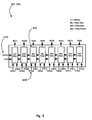
- FIG. 3 illustrates RAM arrays 517, 524, whose function was described above.
- the RAM arrays 517, 524 in this example are 8-bits wide by 16-bits deep. Compared to equivalent flip-flops, a RAM device takes up less space, and has its addressing functionality built into the RAM array rather than being external to the device, as in a flip-flop array.
- Eight RAM devices 610 are packaged in each RAM array 517, 524.
- the lines labeled "A" are a 4-bit addressing input to the array; the lines labeled "WE” indicate write-enable; the lines labeled "WD” indicate write-data; and the lines labeled "RD” indicate read-data.
- the RAM array also takes a clock "CLK” input (at 100 MHz in the present example). The fact that there are 12 10-nsec cycles of the fast (100 MHz) clock within the 122-nsec period of the slower (8.192 MHz) clock allows the steps described to be carried out on the 24 sets of incoming T
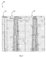
- FIG. 4 illustrates an exemplary data cell format according to one embodiment compatible with the present invention.
- Each cell 700 carries two channels/bytes of data 720, 730 from each of the incoming 24 TDM data streams.
- One TDM frame is therefore carried by 64 cells according to the present exemplary cell format.
- ST denotes a stream number
- CH denotes a channel number within the stream, with “n” being an even number starting with "0”.
- a 2-bit frame number and a 6-bit cell number identifying the cell within the frame are provided in the first byte (byte 0).
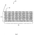
- Figure 5 illustrates an exemplary bit placement table for bits in the RAM arrays 517, 524.
- the cells are written as multiple 32-bit words into the egress synchronous queue 536.
- the table 800 corresponds to the hardware described in the previous figures, and includes 12 rows 810 and 8 columns 820.
- the table is filled with the data as indicated by the stream "ST" and Bit numbers, with the order of filling being in columns, from top to bottom (12 bits 830).
- the RAM arrays are read in rows from left to right (8 bits 840).
Landscapes
- Engineering & Computer Science (AREA)
- Computer Networks & Wireless Communication (AREA)
- Signal Processing (AREA)
- Time-Division Multiplex Systems (AREA)
- Data Exchanges In Wide-Area Networks (AREA)
- Signal Processing For Digital Recording And Reproducing (AREA)
- Synchronisation In Digital Transmission Systems (AREA)
Claims (9)
- System zum Konvertieren wenigstens eines Datenstroms (100) in ein Format einer Datenzelle (700), umfassend:- einen Eingabeprozessor (505), welcher Daten von dem wenigstens einen Datenstrom (100) bei einer ersten Taktfrequenz empfängt und eine Ausgabe des Eingabeprozessors (505) bei einer zweiten Taktfrequenz bereitstellt;- ein Speicherfeld (517), welches die Ausgabe des Eingabeprozessors (505) in einer seriellen Art und Weise empfängt und eine Speicherfeld-Ausgabe (521) in einer parallelen Art und Weise bereitstellt; und- ein Register (525), welches die Speicherfeld-Ausgabe (521) nimmt und eine Mehrzahl von Bits parallel gemäß eines zweiten Formats bereitstellt;dadurch gekennzeichnet, dass die zweite Taktfrequenz schneller als die erste Taktfrequenz ist.
- System nach Anspruch 1, wobei der Eingabeprozessor eine Asynchron-Warteschlange ist.
- System nach Anspruch 2, ferner umfassend einen Multiplexer, welcher zwischen der Asynchron-Warteschlange (505) und dem Speicherfeld (517) angeordnet ist.
- System nach Anspruch 1, wobei das Speicherfeld (517) wenigstens eine RAM-Einheit umfasst, die eine Mehrzahl von Bit-Stellen einschließt.
- System nach Anspruch 2, ferner umfassend eine Synchron-Warteschlange, welche die Mehrzahl der Bits von dem Register (525) empfängt und eine Datenzelle (700) von Ausgabe-Bits bereitstellt.
- System nach Anspruch 1, wobei der wenigstens eine Datenstrom (100) serielle, nach dem Zeitmultiplexverfahren gebündelte TDM-Daten umfasst.
- System nach Anspruch 1, ferner umfassend:- ein Speicherfeld (524), welches Daten in einem ersten Format in einer parallelen Art und Weise empfängt und eine Speicherfeld-Ausgabe (522) in einer seriellen Art und Weise bereitstellt; und- einen Ausgabeprozessor (506), welcher mit dem Speicherfeld (524) gekoppelt ist, das eine Eingabe in einer seriellen Art und Weise bei der zweiten Taktfrequenz empfängt und einen Datenstrom (560) bei der ersten Taktfrequenz und in einem ersten Format (100) ausgibt.
- Verfahren zum Konvertieren wenigstens eines Datenstroms in ein Format einer Datenzelle, umfassend:- Empfangen von Daten von dem wenigstens einen Datenstrom (100) bei einer ersten Taktfrequenz in einer Asynchron-Warteschlange (505) und Bereitstellen einer Asynchron-Warteschlange-Ausgabe bei einer zweiten Taktfrequenz von der Asynchron-Warteschlange (505);- Ablegen der Ausgabe der Asynchron-Warteschlange in ein Speicherfeld (517) in einer seriellen Art und Weise und Bereitstellen einer Speicherfeld-Ausgabe (521) von dem Speicherfeld (517) in einer parallelen Art und Weise; und- Empfangen der Speicherfeld-Ausgabe (521) an einem Register (525) und paralleles Bereitstellen von dem Register (525) einer Mehrzahl von Bits gemäß eines zweiten Formats;dadurch gekennzeichnet, dass die zweite Taktfrequenz schneller als die erste Taktfrequenz ist.
- Verfahren nach Anspruch 8, ferner umfassend:Empfangen von Daten in dem zweiten Format (700) und in einer parallelen Art und Weise und Konvertieren der Daten in ein erstes Format (100) und von einer parallelen Art und Weise in eine serielle Art und Weise zum Ausgeben.
Applications Claiming Priority (2)
| Application Number | Priority Date | Filing Date | Title |
|---|---|---|---|
| US47552103P | 2003-06-03 | 2003-06-03 | |
| PCT/US2004/017287 WO2004109997A1 (en) | 2003-06-03 | 2004-06-03 | System and method for reformatting data |
Publications (2)
| Publication Number | Publication Date |
|---|---|
| EP1636951A1 EP1636951A1 (de) | 2006-03-22 |
| EP1636951B1 true EP1636951B1 (de) | 2008-08-13 |
Family
ID=33511688
Family Applications (1)
| Application Number | Title | Priority Date | Filing Date |
|---|---|---|---|
| EP04753995A Expired - Lifetime EP1636951B1 (de) | 2003-06-03 | 2004-06-03 | System und verfahren zur formatierung von daten |
Country Status (8)
| Country | Link |
|---|---|
| US (1) | US7903685B2 (de) |
| EP (1) | EP1636951B1 (de) |
| JP (1) | JP4594930B2 (de) |
| CN (1) | CN1817011A (de) |
| AT (1) | ATE405073T1 (de) |
| CA (1) | CA2528051C (de) |
| DE (1) | DE602004015792D1 (de) |
| WO (1) | WO2004109997A1 (de) |
Families Citing this family (5)
| Publication number | Priority date | Publication date | Assignee | Title |
|---|---|---|---|---|
| CN1855783B (zh) * | 2005-04-21 | 2011-05-04 | 华为技术有限公司 | 大容量时分多路复用交换芯片的数据处理方法 |
| US9201834B2 (en) | 2011-10-11 | 2015-12-01 | Etron Technology, Inc. | Reconfigurable high speed memory chip module and electronic device with a reconfigurable high speed memory chip module |
| CN103117270B (zh) * | 2011-10-11 | 2015-09-02 | 钰创科技股份有限公司 | 高速记忆芯片模块和电子系统装置 |
| EP3005827A4 (de) * | 2013-06-04 | 2017-01-18 | Attobahn Inc. | Molekulare virale netzwerkarchitektur und entwurf |
| US11889590B2 (en) * | 2013-06-04 | 2024-01-30 | Attobahn, Inc. | System and method for a viral molecular network utilizing mobile devices |
Family Cites Families (18)
| Publication number | Priority date | Publication date | Assignee | Title |
|---|---|---|---|---|
| US5058051A (en) * | 1988-07-29 | 1991-10-15 | Texas Medical Instruments, Inc. | Address register processor system |
| JPH0738592B2 (ja) * | 1988-08-12 | 1995-04-26 | 沖電気工業株式会社 | 変換回路 |
| EP0363053B1 (de) * | 1988-10-06 | 1998-01-14 | Gpt Limited | Asynchrone Zeitvielfachvermittlungsanordnung und Verfahren zum Betrieb der Anordnung |
| JPH0783339B2 (ja) * | 1989-03-01 | 1995-09-06 | 富士通株式会社 | 多重同期回路 |
| JPH04124995A (ja) * | 1990-09-17 | 1992-04-24 | Hitachi Ltd | 2ポートメモリ及びその基本メモリセル並びにそれを用いた直並列変換器及び時間スイッチ |
| JPH06275069A (ja) * | 1993-03-20 | 1994-09-30 | Hitachi Ltd | シリアルメモリ |
| CA2100729C (en) * | 1993-07-16 | 2001-01-16 | Simon Skierszkan | Serial bit rate converter embedded in a switching matrix |
| KR100230230B1 (ko) * | 1993-12-24 | 1999-11-15 | 윤종용 | 메모리 어드레싱 방법 및 장치 |
| US5841771A (en) * | 1995-07-07 | 1998-11-24 | Northern Telecom Limited | Telecommunications switch apparatus and method for time switching |
| US6381239B1 (en) * | 1996-02-13 | 2002-04-30 | Taqua Systems, Inc. | Multiple application switching platform and method |
| US5878045A (en) * | 1996-04-26 | 1999-03-02 | Motorola, Inc. | Method and apparatus for converting data streams in a cell based communications system |
| US5796733A (en) * | 1996-07-03 | 1998-08-18 | General Signal Corporation | Time division switching system |
| US6529510B1 (en) * | 1997-12-19 | 2003-03-04 | Lg Information & Communications, Ltd. | ATM switching apparatus and method thereof |
| US6684275B1 (en) * | 1998-10-23 | 2004-01-27 | Octave Communications, Inc. | Serial-to-parallel/parallel-to-serial conversion engine |
| JP3344401B2 (ja) * | 2000-03-03 | 2002-11-11 | 日本電気株式会社 | ゆらぎバッファ制御装置 |
| US7593432B2 (en) * | 2001-03-31 | 2009-09-22 | Redback Networks Inc. | Method and apparatus for deframing signals |
| US7181485B1 (en) * | 2001-11-26 | 2007-02-20 | Integrated Device Technology, Inc. | Variably delayable transmission of packets between independently clocked source, intermediate, and destination circuits while maintaining orderly and timely processing in one or both of the intermediate and destination circuits |
| CA2366397A1 (en) * | 2001-12-31 | 2003-06-30 | Tropic Networks Inc. | An interface for data transfer between integrated circuits |
-
2004
- 2004-06-03 CA CA2528051A patent/CA2528051C/en not_active Expired - Fee Related
- 2004-06-03 DE DE602004015792T patent/DE602004015792D1/de not_active Expired - Lifetime
- 2004-06-03 EP EP04753995A patent/EP1636951B1/de not_active Expired - Lifetime
- 2004-06-03 AT AT04753995T patent/ATE405073T1/de not_active IP Right Cessation
- 2004-06-03 CN CNA2004800192415A patent/CN1817011A/zh active Pending
- 2004-06-03 US US10/860,365 patent/US7903685B2/en active Active
- 2004-06-03 JP JP2006515068A patent/JP4594930B2/ja not_active Expired - Fee Related
- 2004-06-03 WO PCT/US2004/017287 patent/WO2004109997A1/en not_active Ceased
Also Published As
| Publication number | Publication date |
|---|---|
| JP4594930B2 (ja) | 2010-12-08 |
| EP1636951A1 (de) | 2006-03-22 |
| ATE405073T1 (de) | 2008-08-15 |
| US7903685B2 (en) | 2011-03-08 |
| CA2528051C (en) | 2013-01-22 |
| JP2007526656A (ja) | 2007-09-13 |
| US20050030982A1 (en) | 2005-02-10 |
| CN1817011A (zh) | 2006-08-09 |
| CA2528051A1 (en) | 2004-12-16 |
| WO2004109997A1 (en) | 2004-12-16 |
| DE602004015792D1 (de) | 2008-09-25 |
Similar Documents
| Publication | Publication Date | Title |
|---|---|---|
| EP0363053B1 (de) | Asynchrone Zeitvielfachvermittlungsanordnung und Verfahren zum Betrieb der Anordnung | |
| EP1305691A2 (de) | Sprache-über-ip-kommunikation ohne echolöschung | |
| US6684275B1 (en) | Serial-to-parallel/parallel-to-serial conversion engine | |
| JPH02111138A (ja) | バッファキュー書込みポインタ制御回路 | |
| US20030229734A1 (en) | FIFO scheduling time sharing | |
| JPH08293877A (ja) | 通信システム | |
| JP2738762B2 (ja) | 高速パケット交換機 | |
| EP1384357B1 (de) | Architekturen für einen einstufigen schalter | |
| CA2528051C (en) | System and method for reformatting data | |
| US7436815B2 (en) | Switching system and method having low, deterministic latency | |
| US5796733A (en) | Time division switching system | |
| US7568074B1 (en) | Time based data storage for shared network memory switch | |
| US5546393A (en) | Asynchronous transfer mode data cell routing device for a reverse omega network | |
| CN1232333A (zh) | 异步传输模式信元转换装置及使用该装置的方法 | |
| CN101137246B (zh) | 用于同步数字传输系统中的超大规模数据交叉连接的方法 | |
| NO843557L (no) | Konferansebro-krets | |
| EP1282330B1 (de) | Vorrichtung zur Vermittlung von Zeitmultiplexkanälen | |
| CN100579071C (zh) | 数据汇聚和解析、数据转发以及数据交换的方法 | |
| US7730276B1 (en) | Striping of data into memory of a network data switch to prevent read and write collisions | |
| CN1306768C (zh) | 共享内存地址搜索逻辑装置 | |
| CN101741720A (zh) | 多路信元时隙复用的装置和方法 | |
| US7996604B1 (en) | Class queue for network data switch to identify data memory locations by arrival time | |
| GB2223648A (en) | Asynchronous packet switch | |
| US6973080B1 (en) | System for using indirect memory addressing to perform cross-connecting of data transfers | |
| CN1297296A (zh) | 同步数字传输设备中的超大规模交叉连接装置 |
Legal Events
| Date | Code | Title | Description |
|---|---|---|---|
| PUAI | Public reference made under article 153(3) epc to a published international application that has entered the european phase |
Free format text: ORIGINAL CODE: 0009012 |
|
| 17P | Request for examination filed |
Effective date: 20051223 |
|
| AK | Designated contracting states |
Kind code of ref document: A1 Designated state(s): AT BE BG CH CY CZ DE DK EE ES FI FR GB GR HU IE IT LI LU MC NL PL PT RO SE SI SK TR |
|
| RAP1 | Party data changed (applicant data changed or rights of an application transferred) |
Owner name: STARENT NETWORKS CORPORATION |
|
| DAX | Request for extension of the european patent (deleted) | ||
| 17Q | First examination report despatched |
Effective date: 20061227 |
|
| GRAP | Despatch of communication of intention to grant a patent |
Free format text: ORIGINAL CODE: EPIDOSNIGR1 |
|
| GRAS | Grant fee paid |
Free format text: ORIGINAL CODE: EPIDOSNIGR3 |
|
| GRAA | (expected) grant |
Free format text: ORIGINAL CODE: 0009210 |
|
| AK | Designated contracting states |
Kind code of ref document: B1 Designated state(s): AT BE BG CH CY CZ DE DK EE ES FI FR GB GR HU IE IT LI LU MC NL PL PT RO SE SI SK TR |
|
| REG | Reference to a national code |
Ref country code: GB Ref legal event code: FG4D |
|
| REG | Reference to a national code |
Ref country code: CH Ref legal event code: EP |
|
| REG | Reference to a national code |
Ref country code: IE Ref legal event code: FG4D |
|
| REF | Corresponds to: |
Ref document number: 602004015792 Country of ref document: DE Date of ref document: 20080925 Kind code of ref document: P |
|
| PG25 | Lapsed in a contracting state [announced via postgrant information from national office to epo] |
Ref country code: ES Free format text: LAPSE BECAUSE OF FAILURE TO SUBMIT A TRANSLATION OF THE DESCRIPTION OR TO PAY THE FEE WITHIN THE PRESCRIBED TIME-LIMIT Effective date: 20081124 Ref country code: NL Free format text: LAPSE BECAUSE OF FAILURE TO SUBMIT A TRANSLATION OF THE DESCRIPTION OR TO PAY THE FEE WITHIN THE PRESCRIBED TIME-LIMIT Effective date: 20080813 |
|
| PG25 | Lapsed in a contracting state [announced via postgrant information from national office to epo] |
Ref country code: SI Free format text: LAPSE BECAUSE OF FAILURE TO SUBMIT A TRANSLATION OF THE DESCRIPTION OR TO PAY THE FEE WITHIN THE PRESCRIBED TIME-LIMIT Effective date: 20080813 Ref country code: FI Free format text: LAPSE BECAUSE OF FAILURE TO SUBMIT A TRANSLATION OF THE DESCRIPTION OR TO PAY THE FEE WITHIN THE PRESCRIBED TIME-LIMIT Effective date: 20080813 Ref country code: AT Free format text: LAPSE BECAUSE OF FAILURE TO SUBMIT A TRANSLATION OF THE DESCRIPTION OR TO PAY THE FEE WITHIN THE PRESCRIBED TIME-LIMIT Effective date: 20080813 |
|
| PG25 | Lapsed in a contracting state [announced via postgrant information from national office to epo] |
Ref country code: BE Free format text: LAPSE BECAUSE OF FAILURE TO SUBMIT A TRANSLATION OF THE DESCRIPTION OR TO PAY THE FEE WITHIN THE PRESCRIBED TIME-LIMIT Effective date: 20080813 |
|
| PG25 | Lapsed in a contracting state [announced via postgrant information from national office to epo] |
Ref country code: DK Free format text: LAPSE BECAUSE OF FAILURE TO SUBMIT A TRANSLATION OF THE DESCRIPTION OR TO PAY THE FEE WITHIN THE PRESCRIBED TIME-LIMIT Effective date: 20080813 Ref country code: BG Free format text: LAPSE BECAUSE OF FAILURE TO SUBMIT A TRANSLATION OF THE DESCRIPTION OR TO PAY THE FEE WITHIN THE PRESCRIBED TIME-LIMIT Effective date: 20081113 |
|
| PG25 | Lapsed in a contracting state [announced via postgrant information from national office to epo] |
Ref country code: CZ Free format text: LAPSE BECAUSE OF FAILURE TO SUBMIT A TRANSLATION OF THE DESCRIPTION OR TO PAY THE FEE WITHIN THE PRESCRIBED TIME-LIMIT Effective date: 20080813 Ref country code: SK Free format text: LAPSE BECAUSE OF FAILURE TO SUBMIT A TRANSLATION OF THE DESCRIPTION OR TO PAY THE FEE WITHIN THE PRESCRIBED TIME-LIMIT Effective date: 20080813 Ref country code: RO Free format text: LAPSE BECAUSE OF FAILURE TO SUBMIT A TRANSLATION OF THE DESCRIPTION OR TO PAY THE FEE WITHIN THE PRESCRIBED TIME-LIMIT Effective date: 20080813 Ref country code: PT Free format text: LAPSE BECAUSE OF FAILURE TO SUBMIT A TRANSLATION OF THE DESCRIPTION OR TO PAY THE FEE WITHIN THE PRESCRIBED TIME-LIMIT Effective date: 20090113 |
|
| PLBE | No opposition filed within time limit |
Free format text: ORIGINAL CODE: 0009261 |
|
| STAA | Information on the status of an ep patent application or granted ep patent |
Free format text: STATUS: NO OPPOSITION FILED WITHIN TIME LIMIT |
|
| 26N | No opposition filed |
Effective date: 20090514 |
|
| PG25 | Lapsed in a contracting state [announced via postgrant information from national office to epo] |
Ref country code: EE Free format text: LAPSE BECAUSE OF FAILURE TO SUBMIT A TRANSLATION OF THE DESCRIPTION OR TO PAY THE FEE WITHIN THE PRESCRIBED TIME-LIMIT Effective date: 20080813 |
|
| PG25 | Lapsed in a contracting state [announced via postgrant information from national office to epo] |
Ref country code: IT Free format text: LAPSE BECAUSE OF FAILURE TO SUBMIT A TRANSLATION OF THE DESCRIPTION OR TO PAY THE FEE WITHIN THE PRESCRIBED TIME-LIMIT Effective date: 20080813 |
|
| PG25 | Lapsed in a contracting state [announced via postgrant information from national office to epo] |
Ref country code: SE Free format text: LAPSE BECAUSE OF FAILURE TO SUBMIT A TRANSLATION OF THE DESCRIPTION OR TO PAY THE FEE WITHIN THE PRESCRIBED TIME-LIMIT Effective date: 20081113 Ref country code: MC Free format text: LAPSE BECAUSE OF NON-PAYMENT OF DUE FEES Effective date: 20090630 |
|
| REG | Reference to a national code |
Ref country code: CH Ref legal event code: PL |
|
| PG25 | Lapsed in a contracting state [announced via postgrant information from national office to epo] |
Ref country code: IE Free format text: LAPSE BECAUSE OF NON-PAYMENT OF DUE FEES Effective date: 20090603 Ref country code: CH Free format text: LAPSE BECAUSE OF NON-PAYMENT OF DUE FEES Effective date: 20090630 Ref country code: LI Free format text: LAPSE BECAUSE OF NON-PAYMENT OF DUE FEES Effective date: 20090630 |
|
| PG25 | Lapsed in a contracting state [announced via postgrant information from national office to epo] |
Ref country code: PL Free format text: LAPSE BECAUSE OF FAILURE TO SUBMIT A TRANSLATION OF THE DESCRIPTION OR TO PAY THE FEE WITHIN THE PRESCRIBED TIME-LIMIT Effective date: 20080813 |
|
| PG25 | Lapsed in a contracting state [announced via postgrant information from national office to epo] |
Ref country code: GR Free format text: LAPSE BECAUSE OF FAILURE TO SUBMIT A TRANSLATION OF THE DESCRIPTION OR TO PAY THE FEE WITHIN THE PRESCRIBED TIME-LIMIT Effective date: 20081114 |
|
| PG25 | Lapsed in a contracting state [announced via postgrant information from national office to epo] |
Ref country code: LU Free format text: LAPSE BECAUSE OF NON-PAYMENT OF DUE FEES Effective date: 20090603 |
|
| PG25 | Lapsed in a contracting state [announced via postgrant information from national office to epo] |
Ref country code: HU Free format text: LAPSE BECAUSE OF FAILURE TO SUBMIT A TRANSLATION OF THE DESCRIPTION OR TO PAY THE FEE WITHIN THE PRESCRIBED TIME-LIMIT Effective date: 20090214 |
|
| PG25 | Lapsed in a contracting state [announced via postgrant information from national office to epo] |
Ref country code: TR Free format text: LAPSE BECAUSE OF FAILURE TO SUBMIT A TRANSLATION OF THE DESCRIPTION OR TO PAY THE FEE WITHIN THE PRESCRIBED TIME-LIMIT Effective date: 20080813 |
|
| PG25 | Lapsed in a contracting state [announced via postgrant information from national office to epo] |
Ref country code: CY Free format text: LAPSE BECAUSE OF FAILURE TO SUBMIT A TRANSLATION OF THE DESCRIPTION OR TO PAY THE FEE WITHIN THE PRESCRIBED TIME-LIMIT Effective date: 20080813 |
|
| REG | Reference to a national code |
Ref country code: GB Ref legal event code: 732E Free format text: REGISTERED BETWEEN 20111222 AND 20111223 |
|
| REG | Reference to a national code |
Ref country code: FR Ref legal event code: TP Owner name: CISCO TECHNOLOGY, INC., US Effective date: 20120209 Ref country code: FR Ref legal event code: CJ Effective date: 20120209 |
|
| REG | Reference to a national code |
Ref country code: DE Ref legal event code: R082 Ref document number: 602004015792 Country of ref document: DE Representative=s name: WEICKMANN & WEICKMANN, DE |
|
| REG | Reference to a national code |
Ref country code: DE Ref legal event code: R082 Ref document number: 602004015792 Country of ref document: DE Representative=s name: PATENTANWAELTE WEICKMANN & WEICKMANN, DE Effective date: 20120326 Ref country code: DE Ref legal event code: R081 Ref document number: 602004015792 Country of ref document: DE Owner name: CISCO TECHNOLOGY, INC., SAN JOSE, US Free format text: FORMER OWNER: STARENT NETWORKS CORP., TEWKSBURY, MASS., US Effective date: 20120326 Ref country code: DE Ref legal event code: R082 Ref document number: 602004015792 Country of ref document: DE Representative=s name: WEICKMANN & WEICKMANN PATENTANWAELTE - RECHTSA, DE Effective date: 20120326 Ref country code: DE Ref legal event code: R082 Ref document number: 602004015792 Country of ref document: DE Representative=s name: WEICKMANN & WEICKMANN PATENT- UND RECHTSANWAEL, DE Effective date: 20120326 |
|
| REG | Reference to a national code |
Ref country code: FR Ref legal event code: PLFP Year of fee payment: 13 |
|
| REG | Reference to a national code |
Ref country code: FR Ref legal event code: PLFP Year of fee payment: 14 |
|
| REG | Reference to a national code |
Ref country code: FR Ref legal event code: PLFP Year of fee payment: 15 |
|
| PGFP | Annual fee paid to national office [announced via postgrant information from national office to epo] |
Ref country code: FR Payment date: 20190625 Year of fee payment: 16 |
|
| PGFP | Annual fee paid to national office [announced via postgrant information from national office to epo] |
Ref country code: GB Payment date: 20190627 Year of fee payment: 16 Ref country code: DE Payment date: 20190627 Year of fee payment: 16 |
|
| REG | Reference to a national code |
Ref country code: DE Ref legal event code: R119 Ref document number: 602004015792 Country of ref document: DE |
|
| GBPC | Gb: european patent ceased through non-payment of renewal fee |
Effective date: 20200603 |
|
| PG25 | Lapsed in a contracting state [announced via postgrant information from national office to epo] |
Ref country code: GB Free format text: LAPSE BECAUSE OF NON-PAYMENT OF DUE FEES Effective date: 20200603 Ref country code: FR Free format text: LAPSE BECAUSE OF NON-PAYMENT OF DUE FEES Effective date: 20200630 |
|
| PG25 | Lapsed in a contracting state [announced via postgrant information from national office to epo] |
Ref country code: DE Free format text: LAPSE BECAUSE OF NON-PAYMENT OF DUE FEES Effective date: 20210101 |
|
| P01 | Opt-out of the competence of the unified patent court (upc) registered |
Effective date: 20230525 |