EP1607738A1 - Procédé et dispositif pour l'inspection de plaquettes - Google Patents
Procédé et dispositif pour l'inspection de plaquettes Download PDFInfo
- Publication number
- EP1607738A1 EP1607738A1 EP05104644A EP05104644A EP1607738A1 EP 1607738 A1 EP1607738 A1 EP 1607738A1 EP 05104644 A EP05104644 A EP 05104644A EP 05104644 A EP05104644 A EP 05104644A EP 1607738 A1 EP1607738 A1 EP 1607738A1
- Authority
- EP
- European Patent Office
- Prior art keywords
- wafer
- edge
- image
- optical
- inspected
- Prior art date
- Legal status (The legal status is an assumption and is not a legal conclusion. Google has not performed a legal analysis and makes no representation as to the accuracy of the status listed.)
- Withdrawn
Links
- 238000000034 method Methods 0.000 title claims abstract description 46
- 238000007689 inspection Methods 0.000 title claims abstract description 35
- 230000003287 optical effect Effects 0.000 claims abstract description 70
- 238000005286 illumination Methods 0.000 claims description 48
- 229920002120 photoresistant polymer Polymers 0.000 claims description 24
- 239000002966 varnish Substances 0.000 claims description 19
- 238000001454 recorded image Methods 0.000 claims description 4
- PLXMOAALOJOTIY-FPTXNFDTSA-N Aesculin Natural products OC[C@@H]1[C@@H](O)[C@H](O)[C@@H](O)[C@H](O)[C@H]1Oc2cc3C=CC(=O)Oc3cc2O PLXMOAALOJOTIY-FPTXNFDTSA-N 0.000 claims description 3
- 238000012545 processing Methods 0.000 abstract description 15
- 239000011324 bead Substances 0.000 abstract description 5
- 239000004065 semiconductor Substances 0.000 abstract description 2
- 230000000295 complement effect Effects 0.000 abstract 1
- 229910044991 metal oxide Inorganic materials 0.000 abstract 1
- 150000004706 metal oxides Chemical class 0.000 abstract 1
- 235000012431 wafers Nutrition 0.000 description 107
- 238000003384 imaging method Methods 0.000 description 16
- 238000004519 manufacturing process Methods 0.000 description 9
- 239000000126 substance Substances 0.000 description 8
- 238000004590 computer program Methods 0.000 description 7
- 238000011161 development Methods 0.000 description 7
- 239000011159 matrix material Substances 0.000 description 5
- 239000003973 paint Substances 0.000 description 5
- 230000005855 radiation Effects 0.000 description 5
- 238000000576 coating method Methods 0.000 description 3
- 238000001514 detection method Methods 0.000 description 3
- 238000011835 investigation Methods 0.000 description 3
- 238000003909 pattern recognition Methods 0.000 description 3
- 230000000007 visual effect Effects 0.000 description 3
- 239000011248 coating agent Substances 0.000 description 2
- 230000000052 comparative effect Effects 0.000 description 2
- 238000011109 contamination Methods 0.000 description 2
- 230000007547 defect Effects 0.000 description 2
- 238000012217 deletion Methods 0.000 description 2
- 230000037430 deletion Effects 0.000 description 2
- 238000011156 evaluation Methods 0.000 description 2
- 238000005259 measurement Methods 0.000 description 2
- 239000013307 optical fiber Substances 0.000 description 2
- 239000000969 carrier Substances 0.000 description 1
- 230000000694 effects Effects 0.000 description 1
- 239000000835 fiber Substances 0.000 description 1
- 229910052736 halogen Inorganic materials 0.000 description 1
- 150000002367 halogens Chemical class 0.000 description 1
- 238000002513 implantation Methods 0.000 description 1
- 230000002452 interceptive effect Effects 0.000 description 1
- 230000015654 memory Effects 0.000 description 1
- 229910001507 metal halide Inorganic materials 0.000 description 1
- 150000005309 metal halides Chemical class 0.000 description 1
- 238000003672 processing method Methods 0.000 description 1
- 230000035945 sensitivity Effects 0.000 description 1
- 239000002904 solvent Substances 0.000 description 1
- 230000003595 spectral effect Effects 0.000 description 1
- 238000001228 spectrum Methods 0.000 description 1
- 238000011144 upstream manufacturing Methods 0.000 description 1
- 238000007740 vapor deposition Methods 0.000 description 1
Images


Classifications
-
- G—PHYSICS
- G01—MEASURING; TESTING
- G01N—INVESTIGATING OR ANALYSING MATERIALS BY DETERMINING THEIR CHEMICAL OR PHYSICAL PROPERTIES
- G01N21/00—Investigating or analysing materials by the use of optical means, i.e. using sub-millimetre waves, infrared, visible or ultraviolet light
- G01N21/84—Systems specially adapted for particular applications
- G01N21/88—Investigating the presence of flaws or contamination
- G01N21/95—Investigating the presence of flaws or contamination characterised by the material or shape of the object to be examined
- G01N21/9501—Semiconductor wafers
- G01N21/9503—Wafer edge inspection
-
- G—PHYSICS
- G06—COMPUTING; CALCULATING OR COUNTING
- G06T—IMAGE DATA PROCESSING OR GENERATION, IN GENERAL
- G06T7/00—Image analysis
- G06T7/0002—Inspection of images, e.g. flaw detection
- G06T7/0004—Industrial image inspection
- G06T7/001—Industrial image inspection using an image reference approach
-
- G—PHYSICS
- G01—MEASURING; TESTING
- G01N—INVESTIGATING OR ANALYSING MATERIALS BY DETERMINING THEIR CHEMICAL OR PHYSICAL PROPERTIES
- G01N21/00—Investigating or analysing materials by the use of optical means, i.e. using sub-millimetre waves, infrared, visible or ultraviolet light
- G01N21/84—Systems specially adapted for particular applications
- G01N21/88—Investigating the presence of flaws or contamination
- G01N21/8806—Specially adapted optical and illumination features
- G01N2021/8822—Dark field detection
- G01N2021/8825—Separate detection of dark field and bright field
-
- G—PHYSICS
- G06—COMPUTING; CALCULATING OR COUNTING
- G06T—IMAGE DATA PROCESSING OR GENERATION, IN GENERAL
- G06T2207/00—Indexing scheme for image analysis or image enhancement
- G06T2207/30—Subject of image; Context of image processing
- G06T2207/30108—Industrial image inspection
- G06T2207/30148—Semiconductor; IC; Wafer
Definitions
- the invention relates to a method for inspection of a Wafers, in particular for the investigation of edge varnish, wherein an optical image of the area to be inspected is recorded. Furthermore, the invention relates to a corresponding System with an optical detector for recording an optical image of the area to be inspected. Finally, the invention relates to a computer program and a computer program product for implementing the inspection procedure.
- Edge varnishing can be wet-chemical and / or optical.
- a suitable solvent sprayed on the edge of the wafer, to the optical Randentlackung is the edge exposed specifically and the exposed Area subsequently removed in the development process.
- Border paint defects may be due to inaccurate alignment the corresponding Entlackungsvortechnischen relative to Wafers result. Other sources of error are inaccurate Alignment of the illumination device relative to Wafer during the exposure of the photoresist. Error in the Border paint can be too small or too large Width of the stripped wafer edge or to an eccentric Course of this edge lead. Too little edge varnish may cause contamination in the subsequent Wafer processing lead, however, can be too large Edge varnish to increase rejects due to reduction of the usable wafer range. In both cases the productivity of the manufacturing process is reduced. Therefore it is necessary to make statements about the breadth of Edge varnish to meet. For this it is of interest this after every manufacturing step of the wafer, i. after each application of a photoresist layer followed by Edge varnish, to inspect.
- DE 102 32 781 A1 therefore proposes a system consisting of a reflected light illumination source and an imaging device for inspecting a wafer surface, wherein the illumination device at a suitable angle such turned out of the bright field illumination setting is that an observation of the wafer surface in the dark field he follows.
- This allows mainly small Inspect structures particularly well, characterized by low Distinguish height difference from the ground.
- Object of the present invention is therefore, a method and a system for inspecting a wafer, in particular for Examination of edge varnish to indicate, by means of an optical detector of an optical image of the inspected Area is to be included, and where the to be examined clearly structures to be examined.
- This object is achieved in that a first optical image before applying a layer the wafer disk and a second optical image after the at least partially removed this layer and that the imaged area of the wafer surface inspected by comparing the first and second images becomes.
- the layer to be applied is in practice usually around a photoresist layer (through Applying photoresist) or an antireflection coating. Without limitation of generality is below mainly from a photoresist layer the speech be carried out at the above-described Randentlackung becomes. However, the invention is also for different types Layers that are at least partially removed, such as Antireflection layers, valid.
- the inventive comparison of the first and the second Picture makes it possible, features of previous processes to eliminate. This can cause structures that are out previous process steps, no longer disturbing impact.
- the comparison of the two pictures takes place using appropriate image processing that makes the difference working out between the pictures. This can be z. In easy way done by creating a difference image.
- the application of the photoresist layer ie before application the drop of paint on the rotating wafer disc
- the first optical picture taken. This then shows the actual state the wafer surface as it is due to the preceding Process steps results.
- the type of edge varnish wet-chemical and / or optical
- the second picture shows that by the development of the photoresist relief including the EBR.
- the second picture are also those in the first one Picture existing structures (at least in part) visible. By comparing both images, they can be left over remained structures from the previous process steps eliminate. In the simplest case, this is a difference image However, a weighted difference can also be created or other known image processing methods, to the differences of the two pictures maximum to make recognizable.
- the edge deletion i. So the distance of the paint removal from the wafer edge, better than previously determined can.
- the border width and possibly other variables of interest such as tolerance, measure of Eccentricity, etc., to be determined. It makes sense only to save the result image (eg difference image) or, to further reduce the amount of data, only the certain result values.
- the result image eg difference image
- the certain result values can also be provided be, in hard-to-evaluate problem cases both images to save a subsequent visual follow-up to enable.
- the inventive method can with the known types of lighting operate, the optical images then in the bright field, in the dark field or in the combined light and Darkfield are recorded.
- the area to be inspected may be from an optical detector (Line or matrix detector). Also One-Shots (recording the entire wafer in one image) are appropriate.
- the optical resolution must be the desired Resolution of the areas to be detected (the Width of the Randentlackung) be adapted.
- the too inspecting area can be illuminated monochrome or polychrome.
- the optical Detector can represent a monochrome or color camera.
- a polychrome lighting does not necessarily A color camera ahead, rather, can also be a monochrome camera be used, at least for one area the polychromatic illumination is spectrally sensitive. in the In general, you can work with incident light brightfield illumination become.
- a wafer inspection system is for inspection a wafer, in particular for the investigation of edge varnish, with an optical detector for receiving a optical image of the area to be inspected and with a Data read-out device for reading optical data Detector supplied image data with one with the data read-out device related computer unit to Comparison of recorded images of the inspected Area equipped. It is sufficient and advantageous if the system has a single optical detector, the prior to applying a layer to the wafer wafer a first picture and after at least partial removal this layer takes a second image. The computer unit compares the recorded images and allows them the inventive inspection of the imaged area the wafer surface.
- the wafer can be integrated so that the processed wafer the inspection system once before applying, for example the photoresist layer and then, for example passes through after developing the photoresist.
- the computer unit expediently takes over next to Comparison of image data equal to the determination of the interest Measured variables, such as edge width, tolerance, etc. with.
- a computer program with program code means is expediently in the mentioned computer unit of the inspection system Abariabar to the inventive inspection method perform.
- the computer program suitably an image processing module, the differences between two optical images in for the present Optimally working out wafer inspection, on.
- the computer program has means such as Pattern recognition module, in order to extract from the resulting comparison or difference image the data of interest extract.
- the extracting data count in the case edge deletion inspection the width of the edge, the average deviation from this (tolerance) the measure of Eccentricity of the entblackten edge on the circular wafer wafer etc.
- the determined data can be used in appropriate Be stored, it may be convenient if corresponding when exceeding exceeded tolerances Warning signals or instructions on this occur.
- the computer program may be on suitable data carriers, such as EEPROMs, flash memories, but also CD-ROMs, floppy disks or Hard disk drives stored. Also the download the computer program via internal or public usable networks is possible and known.
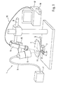
- Figure 1 shows a suitable for the present invention System for wafer inspection, in particular for examination the edge lacquering.
- An optical detector 9, here an imaging device in the form of a CCD line scan camera and a Incident light illumination device 5 are to be inspected Area of the wafer 2 in the area of its wafer edge 23 directed.
- the overall system for wafer inspection is denoted by 1.
- a wafer edge position detection device 22 provided, wherein an adjustment by means of illumination below the wafer 2 is made.
- the recorded by the imaging device 9 Image data is received via a data line 16 a data read-out 17 transmitted.
- This data read-out device 17 is or contains a computer unit 18 for evaluation of recorded images.
- the epi-illumination device 5 to be inspected Area of the wafer edge 23 of the wafer 2 directed.
- Light passes through a light source 7 and an optical fiber bundle 6 in the lighting device 5, the opposite the surface of the wafer 2 is arranged inclined.
- At one displaceable support member 8 is by means of a support rail 15, the imaging device 9 is arranged.
- the axes the imaging device 9 and the illumination device 5 are dashed lines and intersect on the surface of the wafer edge 23.
- the illumination device 5 becomes the imaging device 9 arranged that the dashed line Axes of the two bodies 9 and 5 with the on the surface of the wafer 2 vertical wafer standards at the intersection of the two axes in a common Lie flat.
- the wafer 2 is located on a recording device 3, the wafer 2 by means of Vacuum suction holds.
- the required vacuum is the receiving device 3 is supplied by means of a vacuum line 4.
- the user can the bright field or dark field illumination adapt to the property to be inspected, to optimally map the structure to be examined can.
- the wafer 2 passes through the inspection system 1 twice per Jerusalemssen istszyklus.
- the possibly preprocessed wafer is the first time before the next processing step in the Inspection system 1 introduced where an optical image - in This embodiment of the wafer edge - recorded becomes.
- the usual processing of the Wafers by coating the wafer wafer, curing the paint, Removing the edge bead (EBR), usually by wet chemical Edge varnish (EBR) and depending on the manufacturing process then by optical edge decoating (OEBR), followed by Exposure of the photoresist in the stepper and finally development the photoresist layer to form the desired Reliefs on the wafer surface.
- EBR edge bead
- OEBR optical edge decoating
- the wafer performing the said processing steps usually passes through several times.
- a Examination of the edge decoating takes place according to the invention in each cycle before application of the photoresist layer and after the Randentlackung, so expediently after development the photoresist layer.
- the processed wafer accordingly becomes a second time expediently after development of the photoresist layer, the inspection system 1 supplied to a second optical image of the wafer edge. Will the wafer disk immediately After that, again this can take pictures again as the first image in the next processing cycle serve.
- the image data of the first and second images are transmitted via the data line 16 of the data readout device 17 with Computer unit 18 supplied. There is done by means of image processing a comparison of the first and the second picture, in this embodiment, the width of the edge decoating be shown as accurately as possible on the wafer edge 23 should. In the simplest way, the inventive Comparison of the pictures by subtraction, where a Weighting of the image data of the first and second images can be useful.
- FIG. 2 very schematically shows a first optical image 25 and a second optical image 26, as is typical when examining the Randentlackung with z.
- B a matrix camera in the system 1 described above.
- Figure 2C shows a comparison image 27 showing the differences of the first and second images.
- the first optical image 25 shows structures 28 from previous process steps on the wafer surface, Edges 30 from previous process steps as well as the Wafer edge 29.
- the second optical image 26 ( Figure 2B) shows the image of the same area to be inspected after the Applying a photoresist layer and after the Randentlackung (EWC).
- the resist covered area is indicated at 32, the Resistrand after edge lacquering with 31.
- this second optical Figure 26 Structures based on the previous process steps come, namely the structures 28 and 30. This Structures complicate the automatic inspection of edge varnish and make them partially impossible.
- the illustrated invention enables a fast Throughput of examined wafers within their manufacturing process with minimal space requirements.
- the described Imaging device 9 can also scan x / y or one-shots (recording the entire wafer) used become.
- sources of radiation are, inter alia, fiber lighting, LEDs, fluorescent lamps, halogen lamps, metal halide lamps, Flash lamps or lasers.
- the spectrum of Radiation can be poly- or monochromatic. Also the Spectral range can vary depending on the sensitivity the imaging device 9 in the visual, infrared or in the UV range.
- optical detector 9 are suitable photodiodes, line or matrix cameras, which in turn as monochrome or color cameras, approximately in the form of CCD or CMOS cameras, can be configured.
- the data read-out unit 17 can offer only the results of Inspection store and the actual image data too discard. Should with the existing pictures no results to be calculated or the tolerances to be maintained can be exceeded, for visual follow-up stored in individual cases the different optical images become.
- FIG. 3 schematically shows two optical images as they are e.g. with a line scan camera in a system according to FIG. 1 can be recorded ( Figure 3A and 3B) and a comparison image ( Figure 3C).
- the optical images 25 and 26 may, for example, in a as shown in Figure 1 shown system, in the wafer wafer 2 under a line scan as optical Detector 9 rotates, the imaging axis of the optical Detector 9 preferably perpendicular to the wafer wafer 2 stands. This rotation scan gives you Fig. 25 shows an edge development of that shown in FIG. 2A Structures.
- the first optical image 25 (FIG. 3A) shows structures 28 from previous process steps on the wafer surface and margins 30 from previous process steps. Of the Waferrand is designated 29.
- the edge processing begins here at a mark called Notch or Flat 21, for orientation and calibration purposes is applied to a wafer disk.
- the second optical image 26 ( Figure 3B) shows the image of the same area to be inspected after application of a Photoresist layer and after edge varnish (EBR). Of the Resist-covered area is indicated at 32. To wet chemical and / or optical edge decoating is in the region of the wafer wheel to be inspected is the Resistrand 31 available.
- the second optical image 26 has structures that are known from the preceding FIGS Process steps come, namely the structures 28 and 30. Because of these structures was so far the automatic inspection of edge varnish using an optical Image 26 of the area to be inspected almost impossible. Therefore, according to the invention, the images 25 and 26 subjected to a comparison. For this purpose are preferably Image processing procedures used. In both pictures 25 and 26 common structures are to be used in this Comparison suppressed as possible while new added structures are to be strengthened. In the simplest Case, the comparison can be made by forming a difference Pictures 26 and 25 are done.
- a comparative image 27 according to the invention is shown in FIG. 3C shown.
- the areas 33, their appearance through superimposed resist have been altered, are mitigated too detect.
- the edges 30 are from previous ones Process steps (almost) eliminated and the structures 28 greatly weakened by previous process steps. Clear Resistrand 31 appears in relation to the wafer edge 29.
- the comparison image 27 to ensure that the wafer edge 29 as a reference line preserved.
- the width of the edge lacquering can be measured exactly. In particular, the accurate measurement of edge decoating automated by means of a pattern recognition process become.
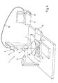
- FIG. 4 shows a wafer inspection system 1 with a similar one Structure of the system of Figure 1.
- the same elements denoted by the same reference numerals.
- the wafer slice 2 is received by a receiving device 3, the one Rotation of the wafer slice 2 around its center allows.
- the receiving device 3 is connected to an x-scan table 11 and connected to a y-scan table 10.
- the combination rotatable Facility 3 and Scant 10 and 11 allows for a an adjustment of the area to be inspected 23 the wafer wafer 2, on the other hand different recording methods, like x-y-scan, the already discussed edge processing (Rotation scan), but also a one-shot of the inspected Area 23 with a matrix camera.
- a bright field illumination device 13 In contrast to the system of Figure 1 is a bright field illumination device 13 with their dashed lines Axially arranged parallel to the surface of the wafer disc 2.
- a beam splitter 12 for example, a semitransparent mirror
- the optical detector 9 is now drawn with its dashed line also Image axis perpendicular to the to be inspected Region 23 arranged.
- a dark field illumination device 14 is provided.
- This device can in principle like the epi-illumination device 5 be configured from Figure 1.
- the dashed axis the dark field illumination device 14 is not parallel to the imaging axis of the optical detector 9, but is inclined to do so. This inclination becomes one Observation in the dark field ensured at the only on investigating structures in the region 23 of the wafer wafer 2 diffracted or scattered radiation on the receiving surface of the optical detector 9 drops.
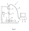
- FIG. 5 essentially shows the wafer inspection system 1 from Figure 4 with changed dark field illumination device 14.
- FIG. 5 essentially shows the wafer inspection system 1 from Figure 4 with changed dark field illumination device 14.
- the dark field illumination device 14 in FIG. 5 it is, for example, a light source with upstream collimating lens system.
- a light source with upstream collimating lens system By this arrangement Ensures that only radiation is dashed from the dash drawn cone of the dark field illumination device 14 on the area to be inspected 23 on the wafer disc 2 meets. Because the optical detector 9 arranged in the center of the illumination device 14 is, an observation in the dark field is ensured. Again, in addition, an observation in the bright field, by the bright field illumination device 13 in Operation is taken.
- FIG. 6 shows the system 1 from FIG. 5 again in one other view (from the side) dar. This is the Beam path of the dark field illumination device 14, represented by the dashed cone and the dashed line imaging axis of the optical Detector 9 clearly visible.
- the bright-field illumination device is not specifically, but on the fastening device for the optical detector 9 and the Dark field illumination device 14 attached. Corresponding the position of the beam splitter 12 is adjusted.
- FIG. 7 shows a further embodiment of the invention System 1 according to Figure 1. Shown here is an embodiment of the system 1 of Figure 1 with an additional Dark field illumination device 14, which combined a Observation in brightfield and darkfield possible. For this becomes the epi-illumination device 5 of the system. 1 from Figure 1 here as a bright field illumination device 13th used. In principle, it can be with the lighting devices 13 and 14 around the same type of lighting equipment (with optical fiber bundle 6 and light source 7) act, but there are also different types of lighting equipment in question.
- the illumination axis of the dark field illumination device 14 is not in this level and is oriented to mirror that plane in the to-be-inspected Area 23 on the wafer slice 2 cuts.
Applications Claiming Priority (2)
| Application Number | Priority Date | Filing Date | Title |
|---|---|---|---|
| DE102004029012A DE102004029012B4 (de) | 2004-06-16 | 2004-06-16 | Verfahren zur Inspektion eines Wafers |
| DE102004029012 | 2004-06-16 |
Publications (1)
| Publication Number | Publication Date |
|---|---|
| EP1607738A1 true EP1607738A1 (fr) | 2005-12-21 |
Family
ID=34940020
Family Applications (1)
| Application Number | Title | Priority Date | Filing Date |
|---|---|---|---|
| EP05104644A Withdrawn EP1607738A1 (fr) | 2004-06-16 | 2005-05-31 | Procédé et dispositif pour l'inspection de plaquettes |
Country Status (5)
| Country | Link |
|---|---|
| US (1) | US20050280807A1 (fr) |
| EP (1) | EP1607738A1 (fr) |
| JP (1) | JP2006005360A (fr) |
| DE (1) | DE102004029012B4 (fr) |
| TW (1) | TW200604517A (fr) |
Cited By (3)
| Publication number | Priority date | Publication date | Assignee | Title |
|---|---|---|---|---|
| US8435593B2 (en) | 2007-05-22 | 2013-05-07 | Asml Netherlands B.V. | Method of inspecting a substrate and method of preparing a substrate for lithography |
| US8492178B2 (en) | 2007-02-23 | 2013-07-23 | Rudolph Technologies, Inc. | Method of monitoring fabrication processing including edge bead removal processing |
| WO2024016380A1 (fr) * | 2022-07-21 | 2024-01-25 | 长鑫存储技术有限公司 | Procédé de traitement, appareil de traitement et système de traitement pour structure semi-conductrice |
Families Citing this family (26)
| Publication number | Priority date | Publication date | Assignee | Title |
|---|---|---|---|---|
| US7280197B1 (en) * | 2004-07-27 | 2007-10-09 | Kla-Tehcor Technologies Corporation | Wafer edge inspection apparatus |
| KR100719367B1 (ko) * | 2005-06-24 | 2007-05-17 | 삼성전자주식회사 | 반도체 제조 장치 및 웨이퍼 가공 방법 |
| JP4413831B2 (ja) * | 2005-08-11 | 2010-02-10 | 株式会社日立ハイテクノロジーズ | ウェハ表面検査装置及びウェハ表面検査方法 |
| JP2007205864A (ja) * | 2006-02-01 | 2007-08-16 | Reitetsukusu:Kk | 基盤検査装置、及び、基盤検査方法 |
| JP5085953B2 (ja) * | 2006-02-24 | 2012-11-28 | 株式会社日立ハイテクノロジーズ | 表面検査装置 |
| EP2023130B1 (fr) * | 2006-05-09 | 2018-03-07 | Nikon Corporation | Dispositif d'inspection de bord |
| JP2007303853A (ja) * | 2006-05-09 | 2007-11-22 | Nikon Corp | 端部検査装置 |
| JP5245212B2 (ja) * | 2006-05-09 | 2013-07-24 | 株式会社ニコン | 端部検査装置 |
| US7616804B2 (en) * | 2006-07-11 | 2009-11-10 | Rudolph Technologies, Inc. | Wafer edge inspection and metrology |
| JP2008032621A (ja) * | 2006-07-31 | 2008-02-14 | Hitachi High-Technologies Corp | 表面検査装置およびその方法 |
| JP5067049B2 (ja) * | 2007-07-12 | 2012-11-07 | 株式会社ニコン | 端部検査装置、及び被検査体の端部検査方法 |
| DE102007042271B3 (de) * | 2007-09-06 | 2009-02-05 | Vistec Semiconductor Systems Gmbh | Verfahren zur Bestimmung der Lage der Entlackungskante eines scheibenförmigen Objekts |
| KR20090055775A (ko) * | 2007-11-29 | 2009-06-03 | 주식회사 동부하이텍 | 반도체 소자의 제조방법 |
| JP5308934B2 (ja) * | 2009-06-29 | 2013-10-09 | オリンパス株式会社 | 基板検査方法および基板検査装置 |
| US20110317003A1 (en) * | 2010-06-02 | 2011-12-29 | Porat Roy | Method and system for edge inspection using a tilted illumination |
| JP5751994B2 (ja) * | 2011-09-02 | 2015-07-22 | ルネサスエレクトロニクス株式会社 | マスクブランクの欠陥検査方法 |
| US9404873B2 (en) * | 2012-03-09 | 2016-08-02 | Kla-Tencor Corp. | Wafer inspection with multi-spot illumination and multiple channels |
| US9809898B2 (en) * | 2013-06-26 | 2017-11-07 | Lam Research Corporation | Electroplating and post-electrofill systems with integrated process edge imaging and metrology systems |
| US9822460B2 (en) | 2014-01-21 | 2017-11-21 | Lam Research Corporation | Methods and apparatuses for electroplating and seed layer detection |
| US9734568B2 (en) * | 2014-02-25 | 2017-08-15 | Kla-Tencor Corporation | Automated inline inspection and metrology using shadow-gram images |
| US9735035B1 (en) | 2016-01-29 | 2017-08-15 | Lam Research Corporation | Methods and apparatuses for estimating on-wafer oxide layer reduction effectiveness via color sensing |
| EP3220101B1 (fr) * | 2016-03-16 | 2020-01-29 | Ricoh Company, Ltd. | Appareil d'évaluation de texture, procédé d'évaluation de texture et support d'enregistrement lisible par ordinateur |
| TWI692049B (zh) * | 2018-08-16 | 2020-04-21 | 江德明 | 晶圓表面檢測前處理裝置及應用其之晶圓表面檢測設備 |
| US11112356B2 (en) * | 2019-07-26 | 2021-09-07 | Photon Control Inc. | Optical reflective edge or contrast sensor |
| JP6788089B2 (ja) * | 2019-10-23 | 2020-11-18 | 東京エレクトロン株式会社 | 基板処理方法、基板処理装置及びコンピュータ読み取り可能な記録媒体 |
| CN111564382A (zh) * | 2020-04-08 | 2020-08-21 | 中国科学院微电子研究所 | 晶圆检测装置及检测方法 |
Citations (6)
| Publication number | Priority date | Publication date | Assignee | Title |
|---|---|---|---|---|
| US5917588A (en) * | 1996-11-04 | 1999-06-29 | Kla-Tencor Corporation | Automated specimen inspection system for and method of distinguishing features or anomalies under either bright field or dark field illumination |
| US6061476A (en) * | 1997-11-24 | 2000-05-09 | Cognex Corporation | Method and apparatus using image subtraction and dynamic thresholding |
| US20020186368A1 (en) * | 2001-06-08 | 2002-12-12 | Eliezer Rosengaus | Systems and methods for inspection of specimen surfaces |
| US20030030050A1 (en) * | 2001-01-26 | 2003-02-13 | Byung-Kon Choi | Apparatus and method of inspecting semiconductor wafer |
| TW540126B (en) * | 2002-03-14 | 2003-07-01 | United Microelectronics Corp | Method of monitoring edge bevel rinse and wafer edge exposure |
| DE10324474A1 (de) * | 2003-05-30 | 2004-12-30 | Leica Microsystems Semiconductor Gmbh | Vorrichtung zur Wafer-Inspektion |
Family Cites Families (9)
| Publication number | Priority date | Publication date | Assignee | Title |
|---|---|---|---|---|
| US4376583A (en) * | 1981-05-12 | 1983-03-15 | Aeronca Electronics, Inc. | Surface inspection scanning system |
| US5293538A (en) * | 1990-05-25 | 1994-03-08 | Hitachi, Ltd. | Method and apparatus for the inspection of defects |
| US6185511B1 (en) * | 1997-11-28 | 2001-02-06 | Advanced Micro Devices, Inc. | Method to accurately determine classification codes for defects during semiconductor manufacturing |
| US7579308B2 (en) * | 1998-07-06 | 2009-08-25 | Ekc/Dupont Electronics Technologies | Compositions and processes for photoresist stripping and residue removal in wafer level packaging |
| DE10027135A1 (de) * | 2000-05-31 | 2001-12-06 | Tokyo Seimitsu Co Ltd | Prüfung von Randabschnitten zweidimensionaler Strukturen |
| DE10131665B4 (de) * | 2001-06-29 | 2005-09-22 | Infineon Technologies Ag | Verfahren und Vorrichtung zur Inspektion des Randbereichs eines Halbleiterwafers |
| US20040032581A1 (en) * | 2002-01-15 | 2004-02-19 | Mehrdad Nikoonahad | Systems and methods for inspection of specimen surfaces |
| WO2003077291A1 (fr) * | 2002-03-12 | 2003-09-18 | Olympus Corporation | Procede de fabrication de semi-conducteurs et dispositif d'usinage associe |
| DE10232781B4 (de) * | 2002-07-18 | 2013-03-28 | Vistec Semiconductor Systems Gmbh | Vorrichtung zur Wafer-Inspektion |
-
2004
- 2004-06-16 DE DE102004029012A patent/DE102004029012B4/de not_active Expired - Fee Related
-
2005
- 2005-05-31 EP EP05104644A patent/EP1607738A1/fr not_active Withdrawn
- 2005-06-14 TW TW094119578A patent/TW200604517A/zh unknown
- 2005-06-15 US US11/153,294 patent/US20050280807A1/en not_active Abandoned
- 2005-06-16 JP JP2005176744A patent/JP2006005360A/ja active Pending
Patent Citations (6)
| Publication number | Priority date | Publication date | Assignee | Title |
|---|---|---|---|---|
| US5917588A (en) * | 1996-11-04 | 1999-06-29 | Kla-Tencor Corporation | Automated specimen inspection system for and method of distinguishing features or anomalies under either bright field or dark field illumination |
| US6061476A (en) * | 1997-11-24 | 2000-05-09 | Cognex Corporation | Method and apparatus using image subtraction and dynamic thresholding |
| US20030030050A1 (en) * | 2001-01-26 | 2003-02-13 | Byung-Kon Choi | Apparatus and method of inspecting semiconductor wafer |
| US20020186368A1 (en) * | 2001-06-08 | 2002-12-12 | Eliezer Rosengaus | Systems and methods for inspection of specimen surfaces |
| TW540126B (en) * | 2002-03-14 | 2003-07-01 | United Microelectronics Corp | Method of monitoring edge bevel rinse and wafer edge exposure |
| DE10324474A1 (de) * | 2003-05-30 | 2004-12-30 | Leica Microsystems Semiconductor Gmbh | Vorrichtung zur Wafer-Inspektion |
Non-Patent Citations (1)
| Title |
|---|
| DATABASE WPI Derwent World Patents Index; AN 2003-894864, XP002343442, CHOU C; LIN D; LIU M; TSAI H; YU C: "Method of monitoring edge bevel rinse and wafer edge exposure" * |
Cited By (3)
| Publication number | Priority date | Publication date | Assignee | Title |
|---|---|---|---|---|
| US8492178B2 (en) | 2007-02-23 | 2013-07-23 | Rudolph Technologies, Inc. | Method of monitoring fabrication processing including edge bead removal processing |
| US8435593B2 (en) | 2007-05-22 | 2013-05-07 | Asml Netherlands B.V. | Method of inspecting a substrate and method of preparing a substrate for lithography |
| WO2024016380A1 (fr) * | 2022-07-21 | 2024-01-25 | 长鑫存储技术有限公司 | Procédé de traitement, appareil de traitement et système de traitement pour structure semi-conductrice |
Also Published As
| Publication number | Publication date |
|---|---|
| DE102004029012B4 (de) | 2006-11-09 |
| TW200604517A (en) | 2006-02-01 |
| JP2006005360A (ja) | 2006-01-05 |
| DE102004029012A1 (de) | 2006-01-12 |
| US20050280807A1 (en) | 2005-12-22 |
Similar Documents
| Publication | Publication Date | Title |
|---|---|---|
| DE102004029012B4 (de) | Verfahren zur Inspektion eines Wafers | |
| DE102004029014B4 (de) | Verfahren und System zur Inspektion eines Wafers | |
| DE60024924T2 (de) | Defektprüfvorrichtung | |
| DE102005028427B3 (de) | Verfahren zur optischen Aufnahme und Inspektion eines Wafers im Rahmen der Randentlackung | |
| DE112017000384T5 (de) | Systeme und Verfahren für erweiterte infrarotspektroskopische Ellipsometrie | |
| EP1756645A1 (fr) | Dispositif et procede d'inspection optique en lumiere reflechie et/ou en lumiere transmise de microstructures en ir | |
| DE3926349C2 (fr) | ||
| DE102009044151B4 (de) | Vorrichtung zur optischen Waferinspektion | |
| DE112017002925T5 (de) | Simultane Mehrwinkel-Spektroskopie | |
| EP1574842A1 (fr) | Méthode ellipsométrique avec correction d'image via recalage | |
| DE2354141A1 (de) | Verfahren zum untersuchen einer oberflaeche und vorrichtung zur durchfuehrung dieses verfahrens | |
| DE112016000853T5 (de) | Optische Metrologie mit reduzierter Empfindlichkeit gegenüber Fokus-Fehlern | |
| DE102006036504A1 (de) | Vorrichtung und Verfahren zur Messung des Höhenprofils eines strukturierten Substrats | |
| DE102016104464B4 (de) | Optische prüfvorrichtung | |
| DE102007039982B3 (de) | Verfahren zur optischen Inspektion und Visualisierung der von scheibenförmigen Objekten gewonnenen optischen Messerwerte | |
| DE10324474A1 (de) | Vorrichtung zur Wafer-Inspektion | |
| DE102005038034B3 (de) | Vorrichtung und Verfahren zur Inspektion der Oberfläche eines Wafers | |
| EP4010145B1 (fr) | Procédé d'analyse de la surface d'une pièce dans le cadre d'un processus d'usinage laser et dispositif d'analyse destiné à analyser la surface d'une pièce | |
| DE102005002267B4 (de) | Verfahren zum Wellenlängenkalibrieren eines optischen Messsystems | |
| DE60115064T2 (de) | Analyseeinrichtung und -verfahren für flüssigkeitshaltige substanzen | |
| DE10323139A1 (de) | Verfahren und Vorrichtung zum Hochauflösenden Fehlerfinden und Klassifizieren | |
| EP3988989A1 (fr) | Procédé et microscope doté d'un dispositif de détection des déplacements d'un échantillon par rapport à une lentille | |
| EP1273878B1 (fr) | Procédé pour détecter un objet en utilisant de résolutions différentes | |
| DE10232781B4 (de) | Vorrichtung zur Wafer-Inspektion | |
| DE112009001936B4 (de) | Inspektionsvorrichtung- und Verfahren für die optische Untersuchung von Objektoberflächen, insbesondere von Waferkanten |
Legal Events
| Date | Code | Title | Description |
|---|---|---|---|
| PUAI | Public reference made under article 153(3) epc to a published international application that has entered the european phase |
Free format text: ORIGINAL CODE: 0009012 |
|
| AK | Designated contracting states |
Kind code of ref document: A1 Designated state(s): AT BE BG CH CY CZ DE DK EE ES FI FR GB GR HU IE IS IT LI LT LU MC NL PL PT RO SE SI SK TR |
|
| AX | Request for extension of the european patent |
Extension state: AL BA HR LV MK YU |
|
| 17P | Request for examination filed |
Effective date: 20060615 |
|
| AKX | Designation fees paid |
Designated state(s): DE FR GB |
|
| RAP1 | Party data changed (applicant data changed or rights of an application transferred) |
Owner name: VISTEC SEMICONDUCTOR SYSTEMS GMBH |
|
| R17C | First examination report despatched (corrected) |
Effective date: 20070419 |
|
| STAA | Information on the status of an ep patent application or granted ep patent |
Free format text: STATUS: THE APPLICATION IS DEEMED TO BE WITHDRAWN |
|
| 18D | Application deemed to be withdrawn |
Effective date: 20070830 |