EP1603153B1 - Procédé d'exposition, procédé de fabrication d'un dispositif et procédé pour afficher des informations - Google Patents
Procédé d'exposition, procédé de fabrication d'un dispositif et procédé pour afficher des informations Download PDFInfo
- Publication number
- EP1603153B1 EP1603153B1 EP04714029.8A EP04714029A EP1603153B1 EP 1603153 B1 EP1603153 B1 EP 1603153B1 EP 04714029 A EP04714029 A EP 04714029A EP 1603153 B1 EP1603153 B1 EP 1603153B1
- Authority
- EP
- European Patent Office
- Prior art keywords
- areas
- substrate
- position information
- higher order
- formula
- Prior art date
- Legal status (The legal status is an assumption and is not a legal conclusion. Google has not performed a legal analysis and makes no representation as to the accuracy of the status listed.)
- Expired - Lifetime
Links
- 238000000034 method Methods 0.000 title claims description 174
- 238000004519 manufacturing process Methods 0.000 title claims description 18
- 238000012937 correction Methods 0.000 claims description 171
- 238000012545 processing Methods 0.000 claims description 96
- 238000004364 calculation method Methods 0.000 claims description 95
- 230000008569 process Effects 0.000 claims description 77
- 239000000758 substrate Substances 0.000 claims description 71
- 238000001514 detection method Methods 0.000 claims description 29
- 238000003860 storage Methods 0.000 claims description 19
- 238000004458 analytical method Methods 0.000 claims description 8
- 238000012546 transfer Methods 0.000 claims description 8
- 238000012935 Averaging Methods 0.000 claims description 6
- 235000012431 wafers Nutrition 0.000 description 154
- 238000005259 measurement Methods 0.000 description 77
- 230000003287 optical effect Effects 0.000 description 31
- 238000003384 imaging method Methods 0.000 description 26
- 238000005286 illumination Methods 0.000 description 22
- 238000013461 design Methods 0.000 description 8
- 230000006870 function Effects 0.000 description 7
- 239000004065 semiconductor Substances 0.000 description 7
- 238000004891 communication Methods 0.000 description 6
- 239000010409 thin film Substances 0.000 description 5
- 230000001594 aberrant effect Effects 0.000 description 4
- 238000001459 lithography Methods 0.000 description 4
- 238000012986 modification Methods 0.000 description 4
- 230000004048 modification Effects 0.000 description 4
- 238000005457 optimization Methods 0.000 description 4
- 239000003504 photosensitizing agent Substances 0.000 description 4
- 230000000694 effects Effects 0.000 description 3
- 239000010408 film Substances 0.000 description 3
- 238000005498 polishing Methods 0.000 description 3
- XUIMIQQOPSSXEZ-UHFFFAOYSA-N Silicon Chemical compound [Si] XUIMIQQOPSSXEZ-UHFFFAOYSA-N 0.000 description 2
- 239000008186 active pharmaceutical agent Substances 0.000 description 2
- 238000004422 calculation algorithm Methods 0.000 description 2
- 238000005229 chemical vapour deposition Methods 0.000 description 2
- 230000001427 coherent effect Effects 0.000 description 2
- 239000006185 dispersion Substances 0.000 description 2
- 238000005530 etching Methods 0.000 description 2
- 238000005339 levitation Methods 0.000 description 2
- 239000004973 liquid crystal related substance Substances 0.000 description 2
- 230000002165 photosensitisation Effects 0.000 description 2
- 230000009467 reduction Effects 0.000 description 2
- 229910052710 silicon Inorganic materials 0.000 description 2
- 239000010703 silicon Substances 0.000 description 2
- 238000000018 DNA microarray Methods 0.000 description 1
- 230000001133 acceleration Effects 0.000 description 1
- 230000004075 alteration Effects 0.000 description 1
- 238000004380 ashing Methods 0.000 description 1
- 201000009310 astigmatism Diseases 0.000 description 1
- 230000008901 benefit Effects 0.000 description 1
- 239000011248 coating agent Substances 0.000 description 1
- 238000000576 coating method Methods 0.000 description 1
- 230000008602 contraction Effects 0.000 description 1
- 230000002950 deficient Effects 0.000 description 1
- 230000001419 dependent effect Effects 0.000 description 1
- 230000006866 deterioration Effects 0.000 description 1
- 238000011161 development Methods 0.000 description 1
- 230000018109 developmental process Effects 0.000 description 1
- 238000006073 displacement reaction Methods 0.000 description 1
- 238000009826 distribution Methods 0.000 description 1
- 238000010894 electron beam technology Methods 0.000 description 1
- 230000008030 elimination Effects 0.000 description 1
- 238000003379 elimination reaction Methods 0.000 description 1
- 230000007717 exclusion Effects 0.000 description 1
- 239000011521 glass Substances 0.000 description 1
- 238000009499 grossing Methods 0.000 description 1
- 229910052736 halogen Inorganic materials 0.000 description 1
- 150000002367 halogens Chemical class 0.000 description 1
- 230000012447 hatching Effects 0.000 description 1
- 238000010884 ion-beam technique Methods 0.000 description 1
- 239000000463 material Substances 0.000 description 1
- 239000011159 matrix material Substances 0.000 description 1
- 230000007246 mechanism Effects 0.000 description 1
- QSHDDOUJBYECFT-UHFFFAOYSA-N mercury Chemical compound [Hg] QSHDDOUJBYECFT-UHFFFAOYSA-N 0.000 description 1
- 229910052753 mercury Inorganic materials 0.000 description 1
- 238000004806 packaging method and process Methods 0.000 description 1
- 239000002245 particle Substances 0.000 description 1
- 229920002120 photoresistant polymer Polymers 0.000 description 1
- 230000008439 repair process Effects 0.000 description 1
- 239000011347 resin Substances 0.000 description 1
- 229920005989 resin Polymers 0.000 description 1
- 230000000087 stabilizing effect Effects 0.000 description 1
- 230000001429 stepping effect Effects 0.000 description 1
- 239000000126 substance Substances 0.000 description 1
Images


Classifications
-
- G—PHYSICS
- G03—PHOTOGRAPHY; CINEMATOGRAPHY; ANALOGOUS TECHNIQUES USING WAVES OTHER THAN OPTICAL WAVES; ELECTROGRAPHY; HOLOGRAPHY
- G03F—PHOTOMECHANICAL PRODUCTION OF TEXTURED OR PATTERNED SURFACES, e.g. FOR PRINTING, FOR PROCESSING OF SEMICONDUCTOR DEVICES; MATERIALS THEREFOR; ORIGINALS THEREFOR; APPARATUS SPECIALLY ADAPTED THEREFOR
- G03F9/00—Registration or positioning of originals, masks, frames, photographic sheets or textured or patterned surfaces, e.g. automatically
- G03F9/70—Registration or positioning of originals, masks, frames, photographic sheets or textured or patterned surfaces, e.g. automatically for microlithography
- G03F9/7003—Alignment type or strategy, e.g. leveling, global alignment
Definitions
- the present invention relates to an exposure method for exposing a substrate suitable for use in a lithography process for production of for example a semiconductor device, liquid crystal display device, CCD, or other imaging device, a plasma display device, thin film magnetic head, or other electronic device (hereinafter simply referred to as an "electronic device”) and an method of display of information. Further, the present invention relates to a method of production of a device using the exposure method.
- a step-and-repeat type, step-and-scan type, or other exposure apparatus, wafer prober, laser repair apparatus, etc. is used.
- These reference positions are for example processing points or other positions defined for processing in different apparatuses and are defined by a stationary coordinate system defining the movement and position of a substrate under processing. Specifically, for example, they are defined by a Cartesian coordinate system defined by laser interferometers etc.
- the semiconductor wafer or glass plate or other substrate has to be aligned with a high accuracy and stability with respect to the projected positions of patterns formed on the mask or reticle (hereinafter simply referred to as a "reticle").
- reticle a high accuracy and stability with respect to the projected positions of patterns formed on the mask or reticle
- 10 or more layers of circuit patterns (reticle patterns) are transferred overlaid on a wafer. Therefore, if the overlay accuracy between the layers is poor, the characteristics of the circuits formed deteriorate. In the worst case, the semiconductor devices have to be discarded as defective and the overall yield is lowered.
- marks arranged in advance at the shot areas on the wafer are used for wafer alignment. That is, alignment marks are arranged in advance at the plurality of shot areas on the wafer.
- the position (coordinate values) on the stage coordinate system (stationary coordinate system) of the alignment mark in a shot area being exposed is detected. Further, the shot area is aligned with respect to the reticle pattern based on the position information of this alignment mark and the position information of a pre-measured reticle pattern.
- D/D die-by-die
- GAA enhanced global alignment
- the positional coordinates of only a plurality of shot areas selected in advance as specific shot areas are measured in one wafer.
- the number of the shot areas has to be three or more and normally is 7 to 15 or so.
- the positional coordinates of all of the shot areas on the -wafer are calculated using the least square method or other statistical processing. Further, the wafer stage is moved in a stepping action in accordance with the calculated arrangement of the shot areas. Therefore, the EGA system has the advantage that the measurement time can be shortened and an effect of averaging random measurement error can be expected.
- EGA EGA system of wafer alignment
- ⁇ Xn ⁇ ⁇ Yn a b c d ⁇ Xn Yn + e f
- the parameters a, b, c, d, e, and f are calculated to minimize the value E of equation (2). Further, the arrangement coordinates of all shot areas on the wafer are calculated based on the calculated parameters a to f and design arrangement coordinates (Xn.Yn).
- the EGA system gives a linear primary approximation of the deviation between a design position and a position actually defined in the wafer and can correct the linear components of elongation, rotation, or other deviation of the wafer.
- stage grid error error between stage coordinate systems between exposure apparatuses. This sometimes causes nonlinear overlay error.
- the wafer suction holding mechanism or suction holding force etc. differs between exposure apparatuses. Due to this, sometimes distortion is given to the wafer. This distortion of the wafer also causes nonlinear deviation, that is, overlay error.
- EGA measurement is performed again based on the EGA results to extract the nonlinear components. Further, the extracted nonlinear components are averaged for a plurality of wafers, and the average value is held as a map correction value. In the subsequent exposure sequences, this map correction value is used for correction of the exposure shot position.
- the nonlinear components are measured for each exposure condition and process using a reference wafer and stored in a map correction file.
- the map correction file in accordance with the exposure conditions is used for correcting the position of each shot area.
- EGA has to be performed for close to all of the shots on each wafer, so the problem arises of deterioration of the throughput.
- a single map correction file is selected for each process (exposure condition) for correction of the nonlinear components, so there is the problem that the nonlinear components of each wafer cannot be corrected at the same exposure sequence.
- US 5 986 766 A describes a global alignment method. As explained in US 5 986 766 A , for any design exposure position (x, y), deviations (d x ', d y ') from this position are predicted using a set of expression corresponding to equations (10).
- the parameters a 00 , b 00 denote substrate displacements in the x- and y-directions respectively, a 10 , b 01 , denote substrate stretching/contraction in the x- and y-directions respectively and a 01 , b 10 denote substrate rotations.
- US 5 863 680 A discloses an exposure method wherein alignment correction parameters are dependent on differing alignment conditions.
- An object of the present invention is to provide an exposure method enabling reduction of the nonlinear components of shot arrangement error and exposure maintaining a good overlay accuracy.
- Still another object of the present invention is to provide a method of production of a device using an exposure process with a good overlay accuracy and a high throughput to enable production of a high quality electronic device efficiently, that is, with a high productivity, and such a high quality device.
- the invention proposes an exposure method as defined in claim 1.
- the method uses the information of the differences between predetermined number calculated position information obtained by calculating position information of a predetermined number of areas among the plurality of areas and predetermined number measured position information obtained by measuring the predetermined number of areas so as to determine the plurality of coefficients of the predetermined calculation formula.
- the method further comprises determining the plurality of coefficients of the predetermined calculation formula so that the differences between the calculated position information and the measured position information become the minimum.
- the method further comprises determining the plurality of coefficients of the predetermined calculation formula so that the sum of squares of the differences between the calculated position information and the measured position information becomes the minimum.
- an alignment method not forming part of the present invention comprises using the calculation formula detected by any method as set forth above to calculate position information of the plurality of areas on the substrate and aligning the plurality of areas on the substrate with predetermined positions.
- the exposure method of the present invention is an exposure method transferring predetermined patterns to a plurality of areas formed on a substrate, comprising using the above alignment method to align the plurality of areas on the substrate with the predetermined patterns and transferring the predetermined patterns to the aligned areas.
- a method of production of a device of the present invention includes a step of using the above exposure method to transfer device patterns to a device substrate.
- an exposure method of the present invention is an exposure method aligning a plurality of areas formed on a substrate with predetermined patterns and exposing the plurality of areas by the predetermined patterns, comprising, in a registration period, using information of the differences between calculated position information obtained by using a first calculation formula provided with second or greater orders and a plurality of coefficients to calculate position information of the plurality of areas and measured position information of the plurality of areas measured in advance to determine the plurality of coefficients of the first calculation formula and storing a second calculation formula for which the plurality of coefficients are determined and, in a processing period after the registration period, reading out a stored second calculation formula, using the read out second calculation formula to calculate the position information of the plurality of areas on the substrate and, based on the calculated position information, aligning the plurality of areas with the predetermined patterns to transfer the predetermined patterns to the aligned areas.
- the method further comprises, in the advanced processing period, measuring the position information of the plurality of areas and storing the measured position information measured in the advanced processing period.
- the method further comprises, after the advanced processing period and before the registration period, measuring the results of positioning between the plurality of areas on the substrate in the advanced processing period and the predetermined patterns and storing the measured position information based on the results of positioning.
- the method further comprises changing the alignment conditions and determining the coefficients of the second calculation formula for each condition in the registration period.
- the method further comprises changing the alignment conditions in accordance with the content of processing performed on the substrate.
- the method further comprises changing the alignment conditions by changing the first calculation formula.
- the method further comprises changing the alignment conditions by changing the number of the calculated position information used for determining the second calculation formula in the registration period and the measured position information.
- the method further comprises using information of the differences between calculated position information obtained by using a first calculation formula provided with a second or greater orders and a plurality of coefficients to calculate position information of a predetermined number of areas among the plurality of areas and measured position information of the read out predetermined number of areas to determine the first calculation formula and storing a second calculation formula for which the plurality of coefficients are determined and changing the alignment conditions by changing the arrangement of the predetermined number of areas.
- the method further comprises forming the measured position information of the plurality of areas by analysis of signal waveforms based on the results of detection of marks formed on the substrate corresponding to the plurality of areas and changing the alignment conditions by changing the method of analysis of the signal waveforms.
- the method further comprises, in the registration period, storing a plurality of the second calculation formulas for which coefficients are determined for each condition and, in the processing period, selecting a specific second calculation formula from the stored plurality of second calculation formulas and using the second calculation formula to calculate the position information for the plurality of areas on the substrate, aligning the plurality of areas with the predetermined patterns based on the calculated position information, and transferring the predetermined patterns to the aligned areas.
- the method further comprises, in the processing period, measuring the position information of the plurality of areas on the substrate and using information of the differences between measured position information of the plurality of areas and calculated position information obtained by using the stored plurality of the second calculation formulas to calculate position information of the plurality of areas so as to select a specific second calculation formula from the plurality of second calculation formulas.
- the method further comprises, in the processing period, detecting information on the trends in arrangement of a plurality of areas on the substrate in the processing period and selecting a specific second calculation formula from the plurality of second calculation formulas based on the detected information of arrangement trends.
- the exposure method further comprises, in the registration period, using information of the differences between the calculated position information obtained by using a plurality of second calculation formulas for which coefficients are determined for each condition to calculate the position information of the plurality of areas and the measured position information so as to selectively store a specific second calculation formula.
- another exposure method of the present invention is an exposure method aligning a plurality of areas formed on a substrate with-predetermined patterns and exposing the plurality of areas by the predetermined patterns, comprising, in a registration period, changing the alignment conditions, using the information of the differences between calculated position information obtained by using a first calculation formula provided with a second or greater orders and a plurality of coefficients for each condition to calculate the position information of the plurality of areas and measured position information of the plurality of areas so as to determine the plurality of coefficients of the first calculation formula and registering these as second calculation formulas, and, in a processing period after the registration period, using the second calculation formulas to calculate position information of the plurality of areas on a substrate, using the calculated position information to align the plurality of areas with the predetermined patterns, and transferring the predetermined patterns to the aligned areas.
- the method further comprises changing the alignment conditions in accordance with the content of processing performed on the substrate.
- the method further comprises changing the alignment conditions by changing the first calculation formula.
- the method further comprises changing the alignment conditions by changing the number of the calculated position information used for determining the second calculation formula in the registration period and the number of the measured position information.
- the method further comprises, in the registration period, changing the alignment conditions, using the information of the differences between calculated position information obtained by using a first calculation formula provided with a second or greater orders and a plurality of coefficients for each condition to calculate position information of a predetermined number of areas among the plurality of areas and measured position information of the predetermined number of areas stored in advance so as to determine the plurality of coefficients of the first calculation formula and storing this as a second calculation formula, and changing the alignment conditions by changing the arrangement of the predetermined number of areas.
- the method further comprises forming the measured position information of the plurality of areas by analysis of signal waveforms based on the results of detection of marks formed on the substrate corresponding to the plurality of areas and changing the alignment conditions by changing the method of analysis of the signal waveforms.
- the method further comprises, in the registration period, storing a plurality of the second calculation formulas and, in the processing period, selecting a specific second calculation formula from the stored plurality of second calculation formulas and using the selected second calculation formula to calculate the position information for the plurality of areas on the substrate, aligning the plurality of areas with the predetermined patterns based on the calculated position information, and transferring the predetermined patterns to the aligned areas.
- the method further comprises, in the processing period, measuring the position information of the plurality of areas on the substrate and using information of the differences between the measured position information of the plurality of areas and calculated position information obtained by using the stored plurality of the second calculation formulas to calculate position information of the plurality of areas so as to select a specific second calculation formula from the plurality of second calculation formulas.
- the method further comprises, in the processing period, detecting information on the trends in arrangement of a plurality of areas on the substrate and selecting a specific second calculation formula from the plurality of second calculation formulas based on the detected information of arrangement trends.
- the method further comprises, in the registration period, using information of the differences between calculated position information obtained by using a plurality of second calculation formulas for which coefficients are determined for each condition to calculate the position information of the plurality of areas and the measured position information so as to selectively store a specific second calculation formula.
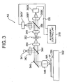
- FIG. 1 is a view of the overall configuration of the exposure system 100 according to the present embodiment.
- the exposure system 100 has N number of exposure apparatuses 200-1 to 200-n, an overlay measurement device 130, and a host computer 140. These devices are connected by a LAN 110 so as to enable the transfer of data. Note that the LAN 110 may also have other processing devices, measurement devices, computers, etc. connected to it to enable transfer of data.
- lot units for example, 1 lot including 25 wafers
- the alignment method according to the present invention enabling correction of nonlinear deviation for each shot area is used for alignment of each shot area.
- the exposure apparatus 200 is connected through the LAN 110 to a host computer 140 controlling the exposure system 100 as a whole and successively processes the wafers for each lot based on instructions from the host computer 140.
- the exposure apparatus 200 is supplied from the host computer 140 with alignment conditions referred to at the time of alignment of the wafers and shot areas.
- the exposure apparatus 200 positions each wafer and shot areas based on the alignment conditions or further selects the optimum conditions from those conditions.
- the exposure apparatus 200 provides the host computer 140 with data (log data) of the results of positioning by the ordinary EGA system performed by the exposure apparatus 200 in accordance with need so the host computer 140 can find the alignment conditions.
- the exposure apparatus 200 is made a step-and-scan type projection exposure apparatus (hereinafter referred to as a scan type exposure apparatus), but it may also be made a step-and repeat type projection exposure apparatus (stepper).
- a scan type exposure apparatus a step-and-scan type projection exposure apparatus
- stepper a step-and repeat type projection exposure apparatus
- the overlay measurement device 130 measures the overlay error of a wafer successively formed with patterns by the exposure apparatus 200.
- the overlay measurement device 130 detects images of registration measurement marks (for example registration images) formed on the wafer, finds the difference in relative positions between marks formed at the time of exposure of different layers, and detects this as the overlay error.
- the overlay measurement device 130 is loaded with wafers formed with patterns and detects the state of overlay when analyzing the results of lot processing, in particular when measurement of overlay error is required.
- the overlay measurement device 130 measures the overlay for wafers loaded after going through specific processes and outputs the measurement results through the LAN 110 to the host computer 140.
- the data of the overlay measurement results is used by the host computer 140 to find the alignment conditions provided to the exposure apparatus 200 in the same way as the data of the EGA measurement results detected at the exposure apparatus 200.
- the host computer 140 is a computer having a large capacity storage device and processing device and controls the overall lithography process in the exposure system 100.
- the host computer 140 has a large capacity storage device which stores information relating to the individual lots or individual wafers processed by the exposure system 100 such as various information for controlling the processes, various parameters or exposure history data, or other various information. Further, based on the information, it controls and manages the exposure apparatuses 200-1 to 200-n so that each lot is suitably processed.
- the host computer 140 finds the alignment conditions used for positioning processing in each exposure apparatus 200-i and registers these in each exposure apparatus 200-i.
- the host computer 140 finds the alignment conditions based on the EGA log data measured by the exposure apparatus 200 or the overlay result data measured by the overlay measurement device 130 or based on the pre-registered design position information or other information of the shot areas.
- One or more alignment conditions are found for each exposure apparatus-i or for each process performed for a lot under exposure. Note that when finding a plurality of alignment conditions, each exposure apparatus 200-i further selects and uses one optimum alignment condition. The method of detection of the alignment conditions will be explained in detail later.
- FIG. 2 is a view of the general configuration of a scan type exposure apparatus as constituted by the exposure apparatus 200.
- the exposure apparatus 200 is provided with an illumination system 210, a reticle stage RST holding a mask constituted by a reticle R, a projection optical system PL, a wafer stage WST on which a substrate constituted by a wafer W is carried, an alignment system AS, a main control system 220 for controlling the apparatus as a whole, etc
- the illumination system 210 has a light source, an optical integrator constituted by a luminance leveling optical system including a fly eye lens or rod integrator (in-plane reflection type integrator), relay lens, variable ND filter, reticle blind, dichroic mirror, etc. (all not shown).
- the illumination system 210 illuminates the slit-shaped illumination areas defined by the reticle blinds on the reticle R drawn by the circuit patterns etc. by the illumination light IL by a substantially uniform luminance.
- the illumination light IL KrF excimer laser light (wavelength 248 nm) or other ultraviolet light, ArF excimer laser light (wavelength 193 nm), F 2 laser light (wavelength 157 nm), or other vacuum ultraviolet light, or ultraviolet band rays (grays, i-rays, etc.) from an extra-high voltage mercury lamp may be used.
- the reticle stage RST has a reticle R fixed to it by for example vacuum suction holding.
- the reticle stage RST is designed to align the reticle R by a not shown reticle stage drive unit comprised of for example a magnetic levitation type two-way linear actuator by means of being able to be driven finely in the XY plane perpendicular to the optical axis of the illumination system 210 (matching with optical axis AX of later explained projection optical system PL) and by being able to be driven at a scan speed designated for a predetermined scan direction (here, made the Y-axis direction).
- the magnetic levitation type two-way linear actuator one including not only a X-drive coil and Y-drive coil, but also a Z-drive coil is used, so the reticle stage RST can also be moved finely in the Z-axis direction.
- the position of the reticle stage RST in the plane of movement of the stage is constantly detected by a reticle laser interferometer (hereinafter called a "reticle interferometer") 216 through a moving mirror 215 by a resolution of for example 0.5 to 1 nm.
- the position information of the reticle stage RST from the reticle interferometer 216 is supplied to the stage control system 219 and through it to the main control system 220.
- the stage control system 219 drives and controls the reticle stage RST in accordance with instructions from the main control system 220 based on position information of the reticle stage RST.
- a pair of reticle alignment systems 222 (reticle alignment system at deep side of figure not shown) are arranged.
- Each of this pair of reticle alignment systems 222 is comprised of an oblique illumination system for illuminating marks for detection by illumination light of the same wavelength as the illumination light IL and an alignment microscope for obtaining images of the marks for detection.
- the alignment microscope includes an imaging optical system and imaging device. The imaging results from the alignment microscope are supplied to the main control system 220.
- deflection mirrors for guiding the detection light from the reticle R to the reticle alignment systems 222 are arranged to be movable.
- drive units are used to make the deflection mirrors retract to the outsides of the paths of the illumination light IL together with the reticle alignment systems 222.
- the projection optical system PL is arranged under the reticle stage RST in FIG. 2 .
- the direction of its optical axis AX is made the Z-axis direction.
- As the projection optical system PL for example, a double telecentric reduction system is used.
- the projection rate of this projection optical system PL is 1/4, 1/5, 1/6, etc. Therefore, if the illumination light IL from the illumination system 210 is used to illuminate the illumination area of the reticle R, the illumination light IL passing through this reticle R is used to form a reduced image (partially inverted image) of the circuit patterns of the reticle R in the illumination area through the projection optical system PL on the surface of the wafer W on which the resist (photosensitizer) is coated.
- the projection optical system PL a refraction system comprised of only a plurality of, for example 10 to 20, refractive optical devices (lens devices) 213 as shown in FIG. 2 is used.
- the plurality of lens devices 213 forming this projection optical system PL are movable lenses able to be driven to shift in the Z-axis direction (optical axis direction of projection optical system PL) and driven in a direction inclined from the XY plane (that is, a direction rotated about the X-axis and a direction rotated about the Y-axis) by not shown drive devices, for example, by piezoelectric actuators etc.
- the imaging characteristic correction controller 248 independently adjusts the voltages supplied to the drive devices based on instructions from the main control system 220 so that the movable lenses are individually driven and the various imaging characteristics of the projection optical system PL (magnification, distortion, astigmatism, comatic aberration, image plane curvature, etc.) are adjusted. Note that, the imaging characteristic correction controller 248 can control the light source to shift the center wavelength of the illumination light IL and, in the same way as movement of the movable lenses, can adjust the imaging characteristics by shifting the center wavelength.
- the wafer stage WST is arranged on a not shown base below the projection optical system PL in FIG. 2 .
- This wafer stage WST has the wafer holder 225 placed on it.
- This wafer holder 225 has the wafer W fixed to it by for example vacuum suction holding etc.
- the wafer holder 225 is able to incline in any direction with respect to the plane perpendicular to the optical axis of the projection optical system PL by not shown drive units and to be able to move finely in the optical axis AX direction (Z-axis direction) of the projection optical system PL. Further, this wafer holder 225 can operate to be finely rotated about the optical axis AX.
- the wafer stage WST is designed to move in not only the scan direction (Y-axis direction), but also to move in the non-scan direction (X-axis direction) perpendicular to the scan direction so as to enable a plurality of shot areas on the wafer W to be positioned at an exposure area conjugate with the illumination area. It engages in an operation to expose the shot areas on the wafer W by scanning and in a step-and-scan operation for movement to an acceleration start position for exposure of shot areas.
- This wafer stage WST is driven in the two X- and Y-directions by a wafer stage drive unit 224 including for example linear motors.
- the position of the wafer stage WST in the XY plane is constantly detected through a moving mirror 217 provided on its top surface by a wafer laser interferometer system 218 at a resolution of for example 0.5 to 1 nm or so.
- the wafer stage WST is provided with a Y-moving mirror having a reflection surface perpendicular to the scan direction (Y-direction) and an X-moving mirror having a
- the wafer laser interferometer 218 is provided with a Y-interferometer emitting an interferometer beam perpendicular to the Y-moving mirror and an X-interferometer emitting an interferometer beam perpendicular to the X-moving mirror.
- a stationary coordinate system (Cartesian coordinate system) defining the movement position of the wafer stage WST is defined by the measurement axes of the Y-interferometer and X-interferometer of the wafer laser interferometer system 218.
- this stationary coordinate system will also be referred to as a "stage coordinate system".
- the end faces of the wafer stage WST may also be polished to a mirror finish to form reflection surfaces for the above-mentioned interferometer beams.
- the position information (or speed information) on the stage coordinate system of the wafer stage WST is supplied to the stage control system 219 and through this to the main control system 220.
- the stage control system 219 controls the wafer stage WST through the wafer stage drive unit 224 in accordance with instructions of the main control system 220 based on the position information (or speed information) of the wafer stage WST.
- the wafer stage WST has a fiduciary mark plate FM fastened to it near the wafer W.
- the surface of this fiduciary mark plate FM is set to the same height as the surface of the wafer W. This surface is formed with fiduciary marks for so-called baseline measurement, fiduciary marks for reticle alignment, and other fiduciary marks of a later explained alignment system.
- the projection optical system PL is provided at its side with an off-axis type alignment system AS.
- this alignment system AS here, for example, an alignment sensor on Field Image Alignment (FIA) system such as disclosed in Japanese Patent Publication No. H2-54103 is used.
- This alignment system AS emits illumination light having a predetermined wavelength band (for example, white light) to the wafer and detects the images of the alignment marks on the wafer and the images of index marks on an index plate formed in a plane conjugate with the wafer formed by an object lens etc. on the light receiving surface of an imaging device (CCD camera etc.)
- the alignment system AS outputs the imaging results of the alignment marks (and fiduciary marks on the fiduciary mark plate FM) toward the main control system 220.
- the exposure apparatus 200 is further provided with an oblique incidence type multipoint focus detection system comprised of a not shown emitting optical system for supplying imaging beams for forming a plurality of slit images toward the best imaging plane of the projection optical system PL in an oblique direction with respect to the direction of the optical axis AX and a not shown receiving optical system for receiving the imaging light beams reflected from the surface of the wafer W through the slits and fastened to a support (not shown) supporting the projection optical system PL.
- this multipoint focus detection system one of a configuration similar to that disclosed in for example Japanese Patent Publication No. H5-190423 , Japanese Patent Publication No. H6-283403 , etc. is used.
- the stage control system 219 drives the wafer holder 225 in the Z-axis direction and direction of inclination based on the wafer position information from this multipoint focus detection system.
- the main control system 20 is configured including a microcomputer or workstation and centrally controls the components of the apparatus.
- the main control system 220 is connected to the above-mentioned LAN 110. Further, in the present embodiment, the hard disk or other storage device or RAM or other memory forming part of the main control system 220 stores a plurality of types of correction conditions (correction coefficients) prepared in advance as a database.
- the alignment system AS has a light source 341, collimater lens 342, beam splitter 344, mirror 346, object lens 348, condensing lens 350, index plate 352, first relay lens 354, beam splitter 356, X-axis second relay lens 358X, X-axis imaging device 360X comprised of a two-dimensional CCD, Y-axis second relay lens 358Y, and Y-axis imaging device 360Y comprised of a two-dimensional CCD.
- a halogen lamp a light source emitting non-photosensitizing light not photosensitizing the photo resist on the wafer and having a broad wavelength distribution having a certain bandwidth (for example 200 nm or so), here, a halogen lamp.
- broadband illumination light is used.
- the illumination light from the light source 341 travels via the collimater lens 342, beam splitter 344, mirror 346, and object lens 348 to near an alignment mark MA on the wafer W.
- the light reflected from the alignment mark MA travels via the object lens 348, mirror 346, beam splitter 344, and condensing lens 350 to the index plate 352, whereby the index plate 352 is formed with an image of the alignment mark MA.
- the light passing through the index plate 352 travels via the first relay lens 354 toward the beam splitter 356.
- the light passing through the beam splitter 356 is focused by the X-axis second relay lens 358X on the imaging surface of the X-axis imaging device 360X, while the light reflected at the beam splitter 356 is focused on the imaging surface of the Y-axis imaging device 360Y by the Y-axis second relay
- the imaging surfaces of the imaging devices 360X and 360Y are formed with images of the alignment mark MA and images of the index mark of the index plate 352 superposed.
- the imaging signals (DS) of the imaging devices 360X and 360Y are supplied to the main control system 220.
- the main control unit 220 is also supplied with measurement values of the wafer laser interferometer 218 through the stage control system 219. Therefore, the main control unit 220 calculates the position of an alignment mark MA on the stage coordinate system based on the imaging signal DS from the alignment system AS and the measurement value of the wafer laser interferometer 218.
- the exposure apparatus 200 selects the correction condition for correcting the nonlinear error at the time of positioning in the host computer 140 and registers this in the exposure apparatus 200 (processing for registration of nonlinear error correction condition).
- the exposure apparatus 200 uses the registered correction condition for successive aligning and shot exposure processing for each lot, each wafer, and each shot (lot processing).
- the processing for registration of the nonlinear error correction condition selects one or more correction conditions preferable for correction of the nonlinear shot arrangement error and registers them at the exposure apparatus 200.
- the one or more correction conditions are registered corresponding to the process condition of the lot for lot processing at the exposure apparatus 200, that is, for each process condition.
- a plurality of conditions including calculation models of correction formulas are designated and pre-measured history data is applied to the conditions so as to find the correction coefficients of the calculation model for each condition and thereby find the correction conditions. Further, among the correction conditions for the plurality of designated conditions, one or more correction conditions with little residual component in the case of application to history data are selected and registered at the exposure apparatus 200.
- condition for finding the correction conditions in the present embodiment, the conditions of the EGA calculation model, order condition, and correction coefficient are considered.
- a six-parameter model, 10-parameter model, in-shot averaging model, or other calculation model may be considered.
- the models able to be designated are limited in accordance with the number of measurement points in a shot. When there is one measurement point in a shot, .normally the six-parameter model is designated. Further, in the case of a model with numerous measurement points in a shot, the 10-parameter model, in-shot averaging model, and six-parameter model using any single point in a shot may be designated.
- the highest order used such as up to the second order term, third order term, or fourth order term, is designated.
- the shot alignment deformation calculation model shown in equation (3) and equation (4) is used, while when designating the second order, the shot alignment deformation calculation model shown in equation (5) and equation (6) is used.
- W x and Wy show positions of the shot center using the wafer center as the origin
- S x and S y show positions of the measurement point using the shot center as the origin
- ⁇ X and ⁇ Y show the distances to be corrected, that is, the positional deviations.
- W x and W y are positions of the measurement points using the wafer center as the origin.
- the condition for the correction coefficients is for example stabilizing the results of higher order correction by excluding the high correlation correction coefficients, that is, setting 0.
- the condition for the correction coefficients is for example stabilizing the results of higher order correction by excluding the high correlation correction coefficients, that is, setting 0.
- the condition for the correction coefficients is for example stabilizing the results of higher order correction by excluding the high correlation correction coefficients, that is, setting 0.
- the high correlation correction coefficients that is, setting 0.
- W x 2 W y and W x W y 2 by excluding the terms W x 2 W y and W x W y 2 from the coefficients W x 3 , W X 2 W y , W x W y 2 , and W y 3 .
- stable results of higher order correction can be obtained in some cases.
- the higher the order the more effective designation of exclusion of the high correlation correction coefficients in some cases. This condition is designated by several variations.
- the above-mentioned EGA calculation model, order condition, and condition of the correction coefficients were used, but various other conditions may also be considered.
- the number of sample shots of the EGA rough measurement used when selecting correction conditions in the later explained lot processing and the arrangement of the sample shots may also be used.
- the condition of being a reference substrate system for alignment based on a reference wafer or an interferometer reference system for alignment based on an interferometer mirror may also be considered.
- the waveform analysis algorithm, slice level, contrast limit value, processing gate width, and condition of being an internal slope type or external slope type may be considered.
- the condition of setting the smoothing and slice level etc. may be considered, while when it is provided with an LIA type alignment system, the condition of the order of the diffraction light etc. may be considered.
- These conditions for finding the correction conditions may be freely set in a manner corresponding to the processing at the exposure apparatus and the changed conditions.
- the history data referred to for selecting the correction conditions either the EGA log file of the exposure apparatus or the log file of the results of overlay measurement is used.
- the EGA log file of the exposure apparatus is data of position measurement by an exposure apparatus using ordinary EGA in past exposure processing using lot processing or a reference wafer under the same process conditions as when using the selected correction conditions.
- the overlay measurement file is data relating to the positional deviation obtained by positioning based on the results of position measurement, exposure, and measurement of the marks or registration images of the results by an overlay measurement device.
- the correction coefficients corresponding to the designations of the different conditions are found by entering the measurement values of the plurality of shot positions for each wafer stored in the EGA log file or overlay measurement file into the calculation models of the different conditions to calculate the different coefficients (correction coefficients) and averaging these for a plurality of wafers. At this time, when there is aberrant data sufficiently separated from the other coefficient values in the found coefficient values, this is excluded when averaging the values.
- the measurement values of the shot positions used at this time are for calculating the trends in shot alignment deviation of the wafer as a whole, use is made of measurement values of a number of samples larger by a certain extent from the number of measured shots by ordinary linear EGA or the number of measured shots at the time of the later mentioned higher order EGA rough measurement or the measured values of all shots.
- the correction conditions for the different designated conditions are found, a plurality of conditions actually giving small residual components after higher order EGA correction at these conditions are selected, the one giving the smallest residual component is selected, and this is registered in the exposure apparatus 200.
- the residual component is evaluated by the residual sum of squares.
- the conditions are changed in various ways to find the optimum correction coefficient for the set calculation model, and the correction condition including the calculation model, its correction coefficients, and other various conditions is registered in the exposure apparatus 200.
- the above-mentioned calculation model, the order condition, the condition of the correction coefficients, and the correction condition having the found correction coefficients finally can be boiled down to the issue of setting correction coefficients for the correction calculation formula having the highest order term in the 10-parameter model. That is, when the calculation algorithm of such a correction calculation formula is set in common at the exposure apparatus 200 as well, simply registering the correction coefficients in the exposure apparatus 200 becomes equivalent to registering the above-mentioned correction condition. Due to this, in the following explanation, registration of the correction condition in the exposure apparatus 200 will sometimes be referred to as simply setting the correction coefficients.
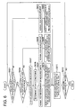
- the various conditions for selecting the correction condition that is, the calculation model to be considered, the condition of the order for optimization by the higher order EGA, and the condition of the correction coefficients for optimization by higher order EGA are set (step S501).
- the conditions are successively designated, the EGA log file or overlay measurement file is referred to for the combinations of these conditions, and the higher order correction coefficients are calculated for a pre-designated predetermined number of wafers.
- the first calculation model is designated as the calculation model (step S502)
- the conditions of the order and correction coefficients are designated (step S503)
- the higher order EGA correction coefficient is calculated (step S504). This is successively performed for a predetermined number of wafers (step S505).
- step S505 After the higher order correction coefficients finish being calculated for a predetermined number of wafers (step S505), aberrant wafer data remarkably separate from the data is rejected (step S506), then the conditions of the order and correction coefficients are set (steps S507 and S503) and then the higher order EGA correction coefficients of a predetermined number of wafers are calculated by the next condition (step S504, S505).
- step S507 After calculating the higher order EGA correction coefficients for all of the set conditions of the order and correction coefficients (step S507), the calculation model is changed (steps S508 and S502), the next calculation model is used for successively setting the conditions of the order and correction coefficients again, and the higher order EGA correction coefficients for a predetermined number of wafers are calculated at each condition (-step S503 to S507).
- the higher order EGA correction coefficients of a predetermined number of wafers are calculated for all of the orders and correction coefficients of all of the set calculation models, that is, for all combinations of the optimization conditions (step S508), then the higher order EGA correction coefficients obtained for the wafers for each optimization condition are averaged (step S509). Note that at step S509, the data remaining after rejecting the aberrant wafer data at step S506 is used.
- the averaged higher order EGA correction coefficient is used to select a predetermined number of higher order EGA correction coefficients from those with small residual sums of squares after correction and these are registered at the exposure apparatus 200 (step S510). At this time, any condition among the conditions of the calculation model/order/correction coefficients may be registered or each condition of wafer deformation may be registered.
- the rejection operation of the aberrant wafer data at step S506 excludes wafer data with a residual sum of squares after higher order correction over a predetermined threshold value in the present embodiment.
- the threshold instead of the residual sum of squares, it is also possible to use as the threshold a decision coefficient (taking value of 0 to 1, the closer to 0, the greater the residual) obtained by dividing the dispersion of the higher order correction position by the dispersion of the measurement result position.
- Each exposure apparatus 200-i set with an alignment correction condition for each process condition not only performs normal EGA processing including linear correction, but also higher order EGA correction, that is, nonlinear component correction, by the set correction condition to align the shot areas of the wafer.
- the linear error as determined by the EGA is corrected by the following calculation model.
- ⁇ X C x ⁇ 10 ⁇ W x + C x ⁇ 10 ⁇ W y + C xsx ⁇ S x + C xsy ⁇ S y + C x ⁇ 00
- ⁇ Y C y ⁇ 10 ⁇ W x + C y ⁇ 10 ⁇ W y + C ysx ⁇ S x + C ysy ⁇ S y + C y ⁇ 00
- W x and W y show positions of the shot center using the wafer center as the origin
- S x and S y show positions of the measurement point using the shot center as the origin
- ⁇ X and ⁇ Y show the amounts of positional correction.
- W x and W y show positions of the measurement point using the wafer center as the origin.
- the coefficient C x10 relates to the X-direction wafer scaling, the coefficient C x01 to wafer rotation, the coefficient C xsx to X-direction shot scaling, the coefficient C xsy to shot rotation, the coefficient C x00 to X-direction offset, the coefficient C y01 to Y-direction wafer scaling, the coefficient C y10 to wafer rotation, the C ysx to shot rotation, the coefficient C ysy to Y-direction shot scaling, and the coefficient C y00 to Y-direction offset.
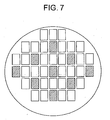
- the higher order EGA rough measurement measures sample shots evenly and roughly designated over the entire region of the wafer.
- the number of the sample shots is greater than the number of shots measured at the time of usual EGA. As an example, nine shots are sampled as shown in FIG. 7 .
- the optimum correction condition is selected by nonlinear correction of the higher order EGA rough shot measurement results for each of the registered plurality of correction conditions, in other words, application of the registered plurality of correction coefficients for higher order correction, and selection of the correction coefficient giving the smallest residual sum of squares.
- the higher order correction coefficients may also be calculated from the higher order EGA rough measurement results, and the coefficients matching the trends in shot arrangement deformation obtained from these may be selected from the registered plurality of correction coefficients.
- this higher order EGA rough measurement may be performed for all wafers of a lot, may be performed for a first predetermined number of wafers of each lot, or may be performed for every other pre-designated number of wafers. At this time, for a wafer not subjected to the higher order EGA rough measurement, it is preferable to use the correction coefficients selected in the higher order EGA rough measurement performed immediately before to perform higher order correction.
- the exposure apparatus 200 uses these inverted in sign.
- the 0-th and 1st components are corrected doubly.
- the 0-th and 1st correction coefficients calculated by ordinary EGA are subtracted from the 0-th -and 1st correction coefficients.
- the presence of any shot component is calculated by matching the conditions between the higher order EGA and ordinary EGA.
- the results of calculation of higher order EGA are used as they are.
- step S601 first it is judged if the higher order EGA rough measurement function is active (on) or inactive (off) (step S601). If inactive, the wafer is measured by ordinary EGA (step S602) and the higher order correction coefficients corresponding to the designated process condition are selected from the pre-registered higher order correction coefficients (step S603). Further, linear correction based on this ordinary EGA measurement result and nonlinear correction by fixed higher order correction coefficients corresponding to the selected process condition are applied for successive aligning and exposure of the shot areas (step S611).
- step S601 When the higher order EGA rough measurement function is active (step S601), it is detected if the wafer being processed is a wafer to be covered by the higher order EGA rough measurement (step S604). Whether a wafer is covered by this higher order EGA rough measurement is set for any one or more wafers based on the wafer positions in the lot as explained above.
- step S604 When the wafer being processed is not a wafer to be covered by the higher order EGA rough measurement (step S604), that wafer is measured by ordinary EGA measurement (step S605) and the higher order EGA correction coefficients used in the exposure of the immediately preceding wafer are selected (step S606). Further, linear correction based on the ordinary EGA measurement results and nonlinear correction by the selected higher order correction coefficients are applied for successive detection and correction of the shot areas, that is, alignment, and exposure (step S611).
- step S604 when the wafer covered by the processing is a wafer to be covered by higher order EGA rough measurement (step S604), higher order EGA rough measurement is performed on the measured shot 930 as shown by the hatching in for example FIG. 7 and the trends in shot arrangement deformation of the wafer 910 are detected (step S607).
- step S608 the single optimum correction coefficient is selected from the plurality of higher order correction coefficients registered for that process condition (step S608). Further, linear correction based on this ordinary EGA measurement result and nonlinear correction by the selected higher order correction coefficient are applied for successive alignment and exposure of the shot areas (step S611).
- step S612 the shot areas in a wafer are successively exposed and all wafers in the lot are exposed.
- the optimum nonlinear correction coefficient (correction condition) is selected in accordance with the trends in nonlinear deformation for each lot or for each wafer, whereby nonlinear deformation is corrected and positioning performed. Therefore, nonlinear error can be corrected in wafer units and accurate positioning is possible. As a result, high accuracy exposure is possible and high quality electronic devices can be produced.
- the correction coefficients are detected by detecting them and registering them in the exposure apparatus in the period before lot processing. Therefore, at the time of lot processing, huge processing for calculating the correction coefficients is not necessary.
- Rough EGA measurement for determining the trends in nonlinear deformation is sufficient.
- shot arrangement need only be measured for nine sample shots or slightly greater than the number of shots in ordinary EGA measurement. Therefore, the effect on the throughput can be suppressed to a minimum, the processing efficiency of the exposure processing can be maintained, and devices can be produced with a high productivity.
- correction coefficients are selected base on the EGA log data or overlay measurement result data or other actual measurement data corresponding to the process condition. Therefore, it is possible to detect a suitable correction coefficient enabling suitable correction of nonlinear error and possible to achieve even more accurate alignment, high definition exposure processing, and production of high quality devices.
- display format it is preferable that display of the measurement values, correction values, residual error after correction using the higher order EGA correction coefficients, etc. can be switched for each shot area on a map like display such as shown in FIG. 7 . Further, this map display preferably enables selective display of the average value for each wafer and for all wafers. Further, as the mode of display for each shot area, it is preferable that display of numerical data and display of a histogram can be selected.
- display of the signal waveforms such as disclosed in for example Japanese Patent Publication No. H4-324615 (Paragraph No. 0066) would be effective for selection of the optimum condition.
- mark position information As the content of the display of the signal waveforms, mark position information, mark detection results, mark detection parameters, mark shape parameters, wafer nos., shot nos., graph display scale, etc. may be mentioned.
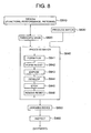
- FIG. 8 is a flow chart of the process of production of for example an IC or LSI or other semiconductor chip, liquid crystal display panel, CCD, thin film magnetic head, micromachine, or other electronic device.
- step S810 in the process of production of an electronic device, first the circuits of the electronic device are designed or the functions and performances of the device are designed and the patterns for realizing these functions are designed (step S810), then a mask for forming the designed circuit patterns is fabricated (step S820).
- silicon or another material is used to produce a wafer (silicon substrate) (step S830).
- step S840 the mask fabricated at step S820 and the wafer produced at step S830 are used for lithography etc. to form the actual circuits etc. on the wafer (step S840).
- the wafer is formed on its surface with an insulating film, electrode interconnect film, and semiconductor film as thin films (step S841), then the entire surface of these thin films is coated by a resist coating device (coater) with a photosensitizer (resist) (step S842).
- a resist coating device coater
- a photosensitizer resist
- the substrate coated with this resist is loaded on a wafer holder of the exposure apparatus according to the present invention
- the-mask produced at step S830 is loaded on a reticle stage
- the patterns formed at the mask are reduced and transferred onto the wafer (step S843).
- the alignment method according to the present invention is used to successively align these at the shot areas of the wafer and successively transfer the patterns of the mask to the shot areas.
- the wafer is unloaded from the wafer holder and a developing apparatus (developer) is used for development (step S844). Due to this, the wafer is formed on its surface with registration images of the mask patterns.
- developer developing apparatus
- step S845 the wafer finished being developed is etched using an etching device (step S845) and the resist remaining on the wafer surface is removed using for example a plasma ashing device etc. (step S846).
- each shot area of the wafer is formed with an insulating layer or electrode interconnects or other patterns. Further, this processing is successively repeated by changing the masks so that the wafer is formed with the actual circuits etc.
- step S850 After the wafer is formed with the circuits etc., it is used to obtain individual devices (step S850). Specifically, the wafer is diced to individual chips which are then mounted in lead frames or packages, bonded with electrodes, and sealed in resin for packaging.
- step S860 the produced devices are tested to confirm their operation, tested for durability, and otherwise inspected (step S860) and then shipped out as finished devices.
- the exposure system is not limited in overall configuration to the configuration shown in FIG. 1 .
- a separate information server 160 may be provided for centrally storing the EGA measurement result data or overlay measurement results and correction coefficients in combination or other various information.
- other computers may be connected to the Intranet 110 to disperse the processing.
- the system may be constructed as a system constructed through a communications network 170 separate from the Intranet 110 or a so-called server client type system.
- the exposure system 102 shown in FIG. 9B is connected with a factory system 103 and server 180 through an external communications network 170.
- the server 180 is equipped with the functions of the host computer 140 and information server 160 in the exposure system 101 of FIG. 9A .
- the factory system 103 has an exposure apparatus 200-i and overlay measurement device 130 for actually processing the wafer and a gateway device constituted by a communications control device 141 for connecting the external communications network 170 and Internet 110.
- the external communications network 170 is for example the Intranet, a communications network using dedicated lines, etc.
- This type of exposure system 102 is preferable when a management division is controlling or managing, for example, a factory system 103 arranged at a far off factory. Further, while not shown, it is preferable when controlling and managing a plurality of factory system 103 by a single server- 180. Further, it may also be applied to a system providing an environment for example for an exposure apparatus manufacturer maintaining characteristics or other information of an exposure apparatus 200 to decide on correction coefficients for a factory system 103 constructed at an electronic device manufacturer through a server 180.
- the mode of sharing the processing for calculation and control and other processing at the different devices of the exposure system in other words, the mode of sharing functions as a dispersed processing system, or the mode of connection of the devices as a network system may be any mode.
- the alignment system the case where an off-axis type FIA system (imaging type alignment system) was used was explained, but the invention is not limited to this. Any type of mark detection system may be used. That is, in addition to a TTR (Through The Reticle) system, TTL (Through The Lens) system, or any other off-axis type system and further an imaging system employing an FIA type detection system (image processing system), for example a system detecting diffraction light or scattered light may be used.
- TTR Through The Reticle
- TTL Through The Lens
- image processing system for example a system detecting diffraction light or scattered light
- an alignment system emitting a coherent beam substantially vertical to an alignment mark on a wafer and causing interference with the same order of diffraction light ( ⁇ 1st order, ⁇ 2n order, ......, ⁇ n-th order diffraction light) from the mark for detection may be used.
- the present invention is not limited to a step-and-scan type exposure apparatus and may be used in exactly the same way for various types of exposure apparatuses such as step-and-repeat type or proximity type exposure apparatuses (X-ray exposure apparatus etc.)
- the exposure illumination light (energy beam) used in the exposure apparatus is not limited to ultraviolet light and may also be X-rays (including EUV light), electron beams or ion beams or other charged particle beams etc. Further, the exposure apparatus may also be one used for production of a DNA chip, mask or reticle, etc.
- the present invention it is possible to provide an alignment method able to reduce the effect on throughput and enabling nonlinear correction for the optical shot alignment for each wafer and an optimum position detection type detection method for the same.
- the present disclosure relates to subject matter contained in Japanese Patent Application No. 2003-049421, filed on February 26, 2003 .
Landscapes
- Physics & Mathematics (AREA)
- General Physics & Mathematics (AREA)
- Exposure And Positioning Against Photoresist Photosensitive Materials (AREA)
- Exposure Of Semiconductors, Excluding Electron Or Ion Beam Exposure (AREA)
Claims (27)
- Procédé d'exposition alignant une pluralité de zones formées sur un substrat (W) avec des motifs prédéterminés et exposant ladite pluralité de zones par l'intermédiaire dudit motif prédéterminé, comportant,
au cours d'une période d'enregistrement (S607, S608),
d'utiliser des informations des différences entre des informations de position calculées obtenues en utilisant une première formule de calcul ayant un second ordre ou un ordre supérieur et une pluralité de coefficients pour calculer des informations de position de la pluralité de zones, et des informations de position mesurées de ladite pluralité de zones mesurées à l'avance afin de déterminer ladite pluralité de coefficients de ladite première formule de calcul et de mémoriser une seconde formule de calcul pour laquelle ladite pluralité de coefficients sont déterminés, et
au cours d'une période de traitement (S609 - S611) après ladite période d'enregistrement,
d'extraire la seconde formule de calcul mémorisée, d'utiliser la seconde formule de calcul extraite pour calculer les informations de position de ladite pluralité de zones sur ledit substrat et, sur la base desdites informations de position calculées, d'aligner ladite pluralité de zones avec lesdits motifs prédéterminés pour transférer lesdits motifs prédéterminés vers lesdites zones alignées,
dans lequel les coefficients déterminés au cours de ladite période d'enregistrement (S607, S608) sont basés sur plus de données de points de mesure que le nombre de points de mesure utilisés lors d'une étape d'alignement (S609) au cours de ladite période de traitement (S609 - S611). - Procédé d'exposition selon la revendication 1, comportant en outre, au cours d'une période de traitement préalable avant ladite période d'enregistrement, de mesurer lesdites informations de position de la pluralité de zones et de mémoriser lesdites informations de position mesurées.
- Procédé d'exposition selon la revendication 1 ou 2, comportant en outre, après ladite période de traitement préalable et avant ladite période d'enregistrement,
de mesurer les résultats de positionnement entre ladite pluralité de zones sur ledit substrat (W) au cours de ladite période de traitement préalable et lesdits motifs prédéterminés, et de mémoriser les informations de position mesurées sur la base des résultats de positionnement. - Procédé d'exposition selon la revendication 2, comportant en outre de changer une condition d'alignement sous laquelle ladite pluralité de zones sur le substrat (W) sont alignées avec lesdits motifs prédéterminés et de déterminer le coefficient de ladite seconde formule de calcul pour chaque condition d'alignement au cours de ladite période d'enregistrement.
- Procédé d'exposition selon la revendication 4, comportant en outre de changer ladite condition d'alignement conformément au traitement exécuté sur ledit substrat.
- Procédé d'exposition selon la revendication 4, comportant en outre de changer ladite condition d'alignement en changeant ladite première formule de calcul.
- Procédé d'exposition selon la revendication 4, comportant en outre de changer ladite condition d'alignement en changeant le nombre desdites informations de position calculées utilisées pour déterminer ladite seconde formule de calcul au cours de ladite période d'enregistrement et desdites informations de position mesurées.
- Procédé d'exposition selon la revendication 4, comportant en outre :d'utiliser des informations des différences entre des informations de position calculées obtenues en utilisant une première formule de calcul ayant un second ordre ou un ordre supérieur et une pluralité de coefficients pour calculer des informations de position d'un nombre prédéterminé de zones parmi ladite pluralité de zones et des informations de position mesurées dudit nombre prédéterminé extrait de zones afin de déterminer ladite première formule de calcul et de mémoriser une seconde formule de calcul pour laquelle ladite pluralité de coefficients sont déterminés, etde changer lesdites conditions d'alignement en changeant l'agencement dudit nombre prédéterminé de zones.
- Procédé d'exposition selon la revendication 4, comportant en outre :de former les informations de position mesurées de ladite pluralité de zones en analysant des formes d'onde de signaux sur la base des résultats de détection de marques formées sur ledit substrat correspondant à ladite pluralité de zones, etde changer lesdites conditions d'alignement en changeant le procédé d'analyse desdites formes d'onde de signaux.
- Procédé d'exposition selon la revendication 4, comportant en outre, au cours de ladite période d'enregistrement,
de mémoriser une pluralités desdites secondes formules de calcul pour lesquelles les coefficients sont déterminés pour chacune desdites conditions, et
au cours de ladite période de traitement,
de sélectionner une seconde formule de calcul parmi ladite pluralité de secondes formules de calcul mémorisées, et
d'utiliser ladite seconde formule de calcul pour calculer les informations de position pour ladite pluralité de zones sur ledit substrat, de positionner ladite pluralité de zones avec lesdits motifs prédéterminés sur la base desdites informations de position calculées, et de transférer lesdits motifs prédéterminés vers lesdites zones alignées. - Procédé d'exposition selon la revendication 10, comportant en outre,
de mesurer lesdites informations de position de la pluralité de zones sur ledit substrat au cours de ladite période de traitement, et
d'utiliser des informations des différences entre des informations de position mesurées de ladite pluralité de zones et des informations de position calculées obtenues en utilisant ladite pluralité desdites secondes formules de calcul mémorisées pour calculer des informations de position de la pluralité de zones de manière à sélectionner une seconde formule de calcul spécifique à partir de la pluralité de secondes formules de calcul. - Procédé d'exposition selon la revendication 10, comportant en outre,
de détecter des informations sur les tendances d'agencement de ladite pluralité de zones sur ledit substrat (W) au cours de ladite période de traitement, et
de sélectionner une seconde formule de calcul spécifique parmi la pluralité de secondes formules de calcul sur la base des informations détectées de tendances d'agencement. - Procédé d'exposition selon la revendication 4, comportant en outre, au cours de ladite période d'enregistrement, d'utiliser des informations des différences entre lesdites informations de position calculées obtenues en utilisant une pluralité de secondes formules de calcul pour lesquelles des coefficients sont déterminés pour chaque condition afin de calculer lesdites informations de position de la pluralité de zones et lesdites informations de position mesurées de manière à mémoriser de manière sélective une seconde formule de calcul spécifique.
- Procédé d'exposition selon la revendication 1, dans lequel des informations de position d'une pluralité de zones d'impact sur un substrat (W) sont calculées et des motifs prédéterminés sur chaque zone d'impact sont exposés tout en commandant la position dudit substrat sur la base desdites informations de position calculées, incluant
une étape (S501) consistant à sélectionner au moins une condition de correction pour corriger une erreur d'alignement non linéaire d'une pluralité de conditions de correction préparées à l'avance pour chaque condition d'une pluralité de conditions de traitement en vue d'un traitement d'exposition du substrat (W),
une étape (S503) consistant à sélectionner au moins une formule de modèle de second ordre ou d'ordre supérieur parmi une pluralité de formules, pour lesquelles des coefficients sont déterminés, mémorisées à l'avance dans un dispositif de mémorisation,
une étape de lecture des données antérieures mémorisées à l'avance sur un dispositif de mémorisation et concernant des résultats de commande de position du substrat (W) sur lequel un premier traitement est exécuté sous une condition sélectionnée parmi lesdites conditions de traitement,
une étape (S504) consistant à traiter lesdits résultats de commande de position sur la base de données spécifiant ladite formule de modèle de second ordre ou d'ordre supérieur sélectionnée, de ladite condition de traitement sélectionnée, et desdits résultats de commande de position lus, et à utiliser les résultats de traitement pour trouver lesdits coefficients de ladite formule de modèle de second ordre ou d'ordre supérieur, et à calculer la formule du second ordre ou d'ordre supérieur pour trouver des informations de position de la pluralité de zones d'impact sur ledit substrat,
une étape consistant à répéter l'étape (S504) de calcul de ladite formule de second ordre ou d'ordre supérieur tout en changeant au moins l'une de ladite condition de correction et de ladite formule de modèle de second ordre ou d'ordre supérieur et à mémoriser dans un dispositif de mémorisation au moins une formule parmi la pluralité de formules de second ordre ou d'ordre supérieur calculées conjointement avec les conditions de traitement associées audit premier traitement,
une étape consistant à extraire des données concernant des résultats d'alignement antérieur du substrat (W) soumis à un second traitement différent dudit premier traitement et mémorisées à l'avance dans ledit dispositif de mémorisation, à calculer la formule de second ordre ou d'ordre supérieur pour ledit second traitement de la même manière que pour calculer la formule de second ordre ou d'ordre supérieur correspondant audit premier traitement, et à mémoriser dans un dispositif de mémorisation la formule de second ordre ou d'ordre supérieur calculée conjointement avec la condition de traitement associée audit second traitement, et
lors d'une nouvelle exécution d'une commande de position pour le substrat (W) soumis au premier traitement, extraire la formule de second ordre ou d'ordre supérieur et les conditions de traitement mémorisées dans ledit dispositif de mémorisation associées audit premier traitement, utiliser ladite formule de second ordre ou d'ordre supérieur extraite et les conditions de traitement pour trouver les informations de position de la pluralité de zones d'impact sur ledit substrat, et exposer des motifs prédéterminés sur la pluralité de zones d'impact sur ledit substrat tout en commandant la position dudit substrat. - Procédé d'exposition selon la revendication 14, dans lequel
la commande de la position dudit substrat inclut une étape consistant à utiliser de manière sélective des données de détection d'un nombre prédéterminé de zones d'impact parmi la pluralité de zones d'impact sur le substrat, et
lesdites conditions de traitement incluent un élément concernant le nombre de zones d'impact dans lesquelles les données de détection sont utilisées. - Procédé d'exposition selon la revendication 14, dans lequel
la commande de la position dudit substrat inclut une étape consistant à utiliser de manière sélective des données de détection de zones d'impact formées selon un agencement prédéterminé parmi la pluralité de zones d'impact sur le substrat, et
lesdites conditions de traitement incluent un élément concernant l'agencement de zones d'impact dans lesquelles les données de détection sont utilisées. - Procédé d'exposition selon la revendication 14, dans lequel
la commande de la position dudit substrat inclut une étape consistant à détecter les images de marques formées correspondant à une pluralité de zones sur le substrat, et
lesdites conditions de traitement incluent un élément concernant le procédé d'analyse de la forme d'onde de signaux desdites images. - Procédé d'exposition selon la revendication 14, dans lequel ledit modèle de second ordre ou d'ordre supérieur est l'un parmi une formule de modèle à 6 paramètres, une formule de modèle à 10 paramètres, et une formule de modèle de mise en moyenne d'impacts.
- Procédé d'exposition selon la revendication 14, dans lequel il existe une pluralité d'ensembles de formules de second ordre ou d'ordre supérieur et de conditions de traitement mémorisées dans ledit dispositif de mémorisation associées à des traitements pour chaque traitement.
- Procédé d'exposition selon la revendication 19, comportant en outre,
lors d'une nouvelle commande de la position d'un substrat, de détecter un nombre spécifique de zones d'impact parmi une pluralité de zones formées sur ledit substrat, et
de sélectionner une formule de second ordre ou d'ordre supérieur spécifique et une condition de traitement à partir de ladite pluralité d'ensembles de formules de second ordre ou d'ordre supérieur et de conditions de traitement mémorisées dans ledit dispositif de mémorisation associées à des traitements sur la base des résultats de détection de ladite pluralité de nombres de zones d'impact. - Procédé de production d'un dispositif par un substrat (W) exposé avec des motifs prédéterminés incluant une étape consistant à exposer ledit substrat auxdits motifs prédéterminés par l'intermédiaire d'un procédé d'exposition selon l'une quelconque des revendications précédentes.
- Procédé d'affichage d'informations concernant une commande de position sur un écran d'affichage dans un procédé d'exposition calculant des informations de position d'une pluralité de zones d'impact sur un substrat (W) et exposant des motifs prédéterminés sur chaque zone d'impact tout en commandant la position dudit substrat sur la base desdites informations de position calculées, incluant
une étape (S501) consistant à sélectionner au moins une condition de correction pour corriger une erreur d'alignement non linéaire d'une pluralité de conditions de correction préparées à l'avance pour chaque condition de la pluralité de conditions de traitement en vue d'un traitement d'exposition du substrat (W),
une étape (S503) consistant à sélectionner au moins une formule de second ordre ou d'ordre supérieur parmi une pluralité de formules pour lesquelles des coefficients sont mémorisés à l'avance dans un dispositif de mémorisation,
une étape consistant à lire des données antérieures mémorisées à l'avance sur un dispositif de mémorisation et concernant des résultats de commande de position du substrat (W) sur lequel un premier traitement est exécuté sous une condition sélectionnée parmi lesdites conditions de traitement,
une étape (S504) consistant à traiter lesdits résultats de commande de position sur la base de données spécifiant ladite formule de modèle de second ordre ou d'ordre supérieur sélectionnée, ladite condition de traitement sélectionnée, et lesdits résultats de commande de position lus, et à utiliser les résultats de traitement pour trouver lesdits coefficients de ladite formule de modèle de second ordre ou d'ordre supérieur, et à calculer la formule de second ordre ou d'ordre supérieur pour trouver des informations de position de la pluralité de zones d'impact sur ledit substrat,
une étape consistant à répéter l'étape (S504) de calcul de ladite formule de second ordre ou d'ordre supérieur tout en changeant au moins l'une de ladite condition de correction et de ladite formule de modèle de second ordre ou d'ordre supérieur et à mémoriser dans un dispositif de mémorisation au moins l'une de la pluralité de formules de second ordre ou d'ordre supérieur calculées conjointement avec la condition de traitement associée audit premier traitement,
une étape consistant à extraire des données concernant des résultats d'alignement antérieur du substrat (W) soumis à un second traitement différent dudit premier traitement et mémorisé à l'avance dans ledit dispositif de mémorisation, à calculer la formule de second ordre ou d'ordre supérieur pour ledit second traitement de la même manière que pour calculer la formule de second ordre ou d'ordre supérieur correspondant audit premier traitement, et à mémoriser dans un dispositif de mémorisation la formule de second ordre ou d'ordre supérieur calculée conjointement avec la condition de traitement associée audit second traitement, et
lors d'une nouvelle exécution d'une commande de position pour le substrat (W) soumis au premier traitement, extraire la formule de second ordre ou d'ordre supérieur et une condition de traitement mémorisée dans ledit dispositif de mémorisation associée audit premier traitement, utiliser ladite formule de second ordre ou d'ordre supérieur extraite et une condition de traitement pour trouver les informations de position de la pluralité de zones d'impact sur ledit substrat, et afficher lesdites informations de position trouvées sur ledit écran d'affichage. - Procédé d'affichage selon la revendication 22, comportant en outre d'afficher les informations de position trouvées conjointement avec une image de l'image de substrat et des images de zones d'impact agencées sur l'image de ladite image de substrat.
- Procédé d'affichage selon la revendication 22, comportant en outre d'afficher les informations de position trouvées par l'intermédiaire de valeurs numériques.
- Procédé d'affichage selon la revendication 22, comportant en outre d'afficher un histogramme basé sur les informations de position trouvées.
- Procédé d'exposition exposant des motifs prédéterminés sur un substrat incluant le procédé d'affichage selon la revendication 22, dans lequel il existe une pluralité d'ensembles de formules de second ordre ou d'ordre supérieur et de conditions de traitement mémorisées dans ledit dispositif de mémorisation associées à des traitements pour chaque traitement.
- Procédé d'exposition selon la revendication 26, comportant en outre de sélectionner une formule de second ordre ou d'ordre supérieur spécifique et une condition de traitement parmi ladite pluralité d'ensembles de formules de second ordre ou d'ordre supérieur et de conditions de traitement mémorisées dans ledit dispositif de mémorisation associées à des traitements sur la base des informations de position affichées sur ledit écran d'affichage.
Applications Claiming Priority (3)
| Application Number | Priority Date | Filing Date | Title |
|---|---|---|---|
| JP2003049421A JP2004265957A (ja) | 2003-02-26 | 2003-02-26 | 最適位置検出式の検出方法、位置合わせ方法、露光方法、デバイス製造方法及びデバイス |
| JP2003049421 | 2003-02-26 | ||
| PCT/JP2004/002116 WO2004077534A1 (fr) | 2003-02-26 | 2004-02-24 | Procede de detection d'equation de detection de position optimale, procede de positionnement, procede d'exposition, procede de fabrication de dispositif et dispositif |
Publications (3)
| Publication Number | Publication Date |
|---|---|
| EP1603153A1 EP1603153A1 (fr) | 2005-12-07 |
| EP1603153A4 EP1603153A4 (fr) | 2008-07-09 |
| EP1603153B1 true EP1603153B1 (fr) | 2013-05-01 |
Family
ID=32923308
Family Applications (1)
| Application Number | Title | Priority Date | Filing Date |
|---|---|---|---|
| EP04714029.8A Expired - Lifetime EP1603153B1 (fr) | 2003-02-26 | 2004-02-24 | Procédé d'exposition, procédé de fabrication d'un dispositif et procédé pour afficher des informations |
Country Status (7)
| Country | Link |
|---|---|
| US (1) | US20060040191A1 (fr) |
| EP (1) | EP1603153B1 (fr) |
| JP (1) | JP2004265957A (fr) |
| KR (1) | KR101022680B1 (fr) |
| CN (1) | CN1751378B (fr) |
| TW (1) | TW200507136A (fr) |
| WO (1) | WO2004077534A1 (fr) |
Families Citing this family (35)
| Publication number | Priority date | Publication date | Assignee | Title |
|---|---|---|---|---|
| KR101060982B1 (ko) * | 2003-11-28 | 2011-08-31 | 가부시키가이샤 니콘 | 노광 방법 및 디바이스 제조 방법, 노광 장치, 그리고 프로그램을 기록한 컴퓨터 판독가능 기록 매체 |
| KR101191057B1 (ko) | 2004-08-19 | 2012-10-15 | 가부시키가이샤 니콘 | 얼라인먼트 정보 표시 방법과 그 프로그램, 얼라인먼트방법, 노광 방법, 디바이스 제조 방법, 표시 시스템, 표시장치, 프로그램 및 측정/검사 장치 |
| WO2006030727A1 (fr) * | 2004-09-14 | 2006-03-23 | Nikon Corporation | Procédé de correction et dispositif d’exposition |
| JP2006148013A (ja) * | 2004-11-24 | 2006-06-08 | Nikon Corp | 位置合わせ方法及び露光方法 |
| US7126669B2 (en) * | 2004-12-27 | 2006-10-24 | Asml Netherlands B.V. | Method and system for automated process correction using model parameters, and lithographic apparatus using such method and system |
| DE102005006239A1 (de) * | 2005-02-10 | 2006-08-17 | Leica Microsystems Cms Gmbh | Vorrichtung zur Einstellung der Divergenz und/oder Konvergenz eines Lichtstrahls |
| EP1744217B1 (fr) * | 2005-07-12 | 2012-03-14 | ASML Netherlands B.V. | Procédé de sélection d'un modèle de grille pour corriger les déformations de la grille dans un appareil lithographique et ensemble lithographique l'utilisant |
| KR101440630B1 (ko) * | 2006-01-26 | 2014-09-15 | 가부시키가이샤 니콘 | 중첩 관리 방법 및 장치, 처리 장치, 측정 장치 및 노광 장치, 디바이스 제조 시스템 및 디바이스 제조 방법, 및 정보 기록 매체 |
| KR100724579B1 (ko) * | 2006-02-01 | 2007-06-04 | 삼성전자주식회사 | 웨이퍼 프리 얼라인먼트 유니트를 갖는 노광설비 및 이를이용한 웨이퍼 프리 얼라인먼트 방법 |
| JP4589998B2 (ja) * | 2006-05-10 | 2010-12-01 | 株式会社目白プレシジョン | 投影露光装置及び投影露光方法 |
| JP2009094265A (ja) * | 2007-10-09 | 2009-04-30 | Canon Inc | マーク位置検出方法および装置 |
| TWI382187B (zh) * | 2008-05-27 | 2013-01-11 | Aerospace Ind Dev Corp | 磁浮自動逆向工程設備及其檢測之方法 |
| JP5264406B2 (ja) * | 2008-10-22 | 2013-08-14 | キヤノン株式会社 | 露光装置、露光方法およびデバイスの製造方法 |
| US8260449B2 (en) | 2008-11-06 | 2012-09-04 | Micron Technology, Inc. | Photolithography systems and associated methods of overlay error correction |
| US9052604B2 (en) * | 2008-11-06 | 2015-06-09 | Micron Technology, Inc. | Photolithography systems and associated alignment correction methods |
| JP2010186918A (ja) * | 2009-02-13 | 2010-08-26 | Nikon Corp | アライメント方法、露光方法及び露光装置、デバイス製造方法、並びに露光システム |
| US7977655B2 (en) * | 2009-05-21 | 2011-07-12 | Taiwan Semiconductor Manufacturing Company, Ltd. | Method and system of monitoring E-beam overlay and providing advanced process control |
| JP5903891B2 (ja) * | 2010-01-18 | 2016-04-13 | 株式会社ニコン | 露光方法、露光装置、及びデバイス製造方法 |
| JP2012089591A (ja) * | 2010-10-18 | 2012-05-10 | Hitachi High-Technologies Corp | 真空処理装置及び真空処理方法 |
| CN103365124B (zh) * | 2012-03-31 | 2015-01-21 | 中芯国际集成电路制造(上海)有限公司 | 曝光对准方法 |
| CN102929105A (zh) * | 2012-11-13 | 2013-02-13 | 美迪亚印刷设备(杭州)有限公司 | 曝光质量检测方法 |
| WO2015081167A1 (fr) | 2013-11-27 | 2015-06-04 | Tokyo Electron Limited | Système et procédé de réglage de substrat au moyen d'une projection optique |
| US9645391B2 (en) | 2013-11-27 | 2017-05-09 | Tokyo Electron Limited | Substrate tuning system and method using optical projection |
| JP6418744B2 (ja) * | 2014-01-23 | 2018-11-07 | キヤノン株式会社 | パターン形成方法、リソグラフィ装置およびシステム、ならびに物品製造方法 |
| US10661101B2 (en) * | 2015-07-01 | 2020-05-26 | Hitachi, Ltd. | Dose distribution calculation device, particle beam therapy system, and dose distribution calculation method |
| WO2017060054A1 (fr) * | 2015-10-08 | 2017-04-13 | Asml Netherlands B.V. | Procédé de commande d'un appareil lithographique et procédé de fabrication de dispositif, système de commande pour appareil lithographique et appareil lithographique |
| US10133193B2 (en) * | 2016-07-19 | 2018-11-20 | Applied Materials, Inc. | Piecewise alignment modeling method |
| US10692227B2 (en) * | 2017-01-05 | 2020-06-23 | Kla-Tencor Corporation | Determination of sampling maps for alignment measurements based on reduction of out of specification points |
| JP7023062B2 (ja) * | 2017-07-24 | 2022-02-21 | 株式会社荏原製作所 | 基板研磨装置及び方法 |
| CN109146956B (zh) * | 2018-08-09 | 2021-11-16 | 厦门市计量检定测试院 | 一种视觉定位系统的线性误差修正系数获取方法 |
| US11011435B2 (en) * | 2018-11-20 | 2021-05-18 | Asm Technology Singapore Pte Ltd | Apparatus and method inspecting bonded semiconductor dice |
| JP7369529B2 (ja) * | 2019-02-28 | 2023-10-26 | 株式会社オーク製作所 | 露光装置およびアライメント方法 |
| CN110045582B (zh) * | 2019-04-19 | 2020-12-18 | 东莞市多普光电设备有限公司 | 一种基于数字微镜ldi的装置及倾斜扫描方法 |
| TWI738510B (zh) * | 2020-09-15 | 2021-09-01 | 倍利科技股份有限公司 | 半導體元件圖像疊合方法 |
| CN113178408A (zh) * | 2021-05-28 | 2021-07-27 | 重庆翰博显示科技研发中心有限公司 | 一种微型电子组件排料转移定位装置及其工作方法 |
Family Cites Families (8)
| Publication number | Priority date | Publication date | Assignee | Title |
|---|---|---|---|---|
| US5561606A (en) * | 1991-08-30 | 1996-10-01 | Nikon Corporation | Method for aligning shot areas on a substrate |
| JP3219217B2 (ja) * | 1993-01-22 | 2001-10-15 | 株式会社ニコン | 位置合わせ方法及び装置、並びに露光方法及び装置 |
| US5525808A (en) * | 1992-01-23 | 1996-06-11 | Nikon Corporaton | Alignment method and alignment apparatus with a statistic calculation using a plurality of weighted coordinate positions |
| JP3287047B2 (ja) * | 1993-02-08 | 2002-05-27 | 株式会社ニコン | 位置合わせ方法、その位置合わせ方法を用いた露光方法、その露光方法を用いたデバイス製造方法、そのデバイス製造方法で製造されたデバイス、並びに位置合わせ装置、その位置合わせ装置を備えた露光装置 |
| JP3258178B2 (ja) * | 1994-09-27 | 2002-02-18 | 株式会社東芝 | 位置合わせ方法 |
| JPH09115817A (ja) * | 1995-10-13 | 1997-05-02 | Nikon Corp | 露光方法及び装置 |
| JP3634487B2 (ja) * | 1996-02-09 | 2005-03-30 | キヤノン株式会社 | 位置合せ方法、位置合せ装置、および露光装置 |
| JP3595707B2 (ja) * | 1998-10-23 | 2004-12-02 | キヤノン株式会社 | 露光装置および露光方法 |
-
2003
- 2003-02-26 JP JP2003049421A patent/JP2004265957A/ja active Pending
-
2004
- 2004-02-24 KR KR1020057015828A patent/KR101022680B1/ko active IP Right Grant
- 2004-02-24 WO PCT/JP2004/002116 patent/WO2004077534A1/fr active Application Filing
- 2004-02-24 EP EP04714029.8A patent/EP1603153B1/fr not_active Expired - Lifetime
- 2004-02-24 CN CN2004800047924A patent/CN1751378B/zh not_active Expired - Fee Related
- 2004-02-26 TW TW093104866A patent/TW200507136A/zh not_active IP Right Cessation
-
2005
- 2005-08-25 US US11/210,879 patent/US20060040191A1/en not_active Abandoned
Also Published As
| Publication number | Publication date |
|---|---|
| TW200507136A (en) | 2005-02-16 |
| JP2004265957A (ja) | 2004-09-24 |
| TWI342057B (fr) | 2011-05-11 |
| KR101022680B1 (ko) | 2011-03-22 |
| EP1603153A4 (fr) | 2008-07-09 |
| US20060040191A1 (en) | 2006-02-23 |
| CN1751378A (zh) | 2006-03-22 |
| KR20050098963A (ko) | 2005-10-12 |
| EP1603153A1 (fr) | 2005-12-07 |
| WO2004077534A1 (fr) | 2004-09-10 |
| CN1751378B (zh) | 2010-06-23 |
Similar Documents
| Publication | Publication Date | Title |
|---|---|---|
| EP1603153B1 (fr) | Procédé d'exposition, procédé de fabrication d'un dispositif et procédé pour afficher des informations | |
| US8982320B2 (en) | Alignment information display method and its program, alignment method, exposure method, device production process, display system, display device, and program and measurement/inspection system | |
| US8539394B2 (en) | Method and apparatus for minimizing overlay errors in lithography | |
| JP4905617B2 (ja) | 露光方法及びデバイス製造方法 | |
| US7817242B2 (en) | Exposure method and device manufacturing method, exposure apparatus, and program | |
| US20020037460A1 (en) | Stage unit, measurement unit and measurement method, and exposure apparatus and exposure method | |
| JP4443537B2 (ja) | リソグラフィ装置又はその一部を較正又は検定する方法及びデバイス製造方法 | |
| US20060033916A1 (en) | Selection method, exposure method, selection unit, exposure apparatus, and device manufacturing method | |
| JP3950082B2 (ja) | リソグラフィ装置およびデバイスを製造する方法 | |
| US20090128792A1 (en) | Lithographic apparatus and method | |
| JP2011119457A (ja) | 位置合わせ条件最適化方法及びシステム、パターン形成方法及びシステム、露光装置、デバイス製造方法、並びに重ね合わせ精度評価方法及びシステム | |
| US20030020889A1 (en) | Stage unit, measurement unit and measurement method, and exposure apparatus and exposure method | |
| JP5838594B2 (ja) | ダブルパターニング最適化方法及びシステム、パターン形成方法、露光装置、並びにデバイス製造方法 | |
| JP2004200632A (ja) | 位置検出方法、露光方法及び露光装置、デバイス製造方法、並びにプログラム及び情報記録媒体 | |
| JP2006148013A (ja) | 位置合わせ方法及び露光方法 | |
| US20100309486A1 (en) | Pattern transfer apparatus and method of manufacturing device | |
| JPH1050600A (ja) | 投影露光方法及び投影露光装置 | |
| JP4596166B2 (ja) | 位置検出方法、露光方法、位置検出装置、露光装置及びデバイス製造方法 | |
| JP4461908B2 (ja) | 位置合わせ方法、位置合わせ装置、及び露光装置 | |
| JPH11233424A (ja) | 投影光学装置、収差測定方法、及び投影方法、並びにデバイス製造方法 | |
| JP2005064369A (ja) | 最適化方法、露光方法、最適化装置、露光装置、デバイス製造方法、及びプログラム、並びに情報記録媒体 | |
| JP2012079735A (ja) | マスク伸縮補正最適化方法、露光方法及びデバイス製造方法、並びにデバイス製造システム | |
| JP2004087562A (ja) | 位置検出方法及びその装置、露光方法及びその装置、並びにデバイス製造方法 | |
| JP2013254849A (ja) | パターン形成最適化方法及びシステム、露光方法及び装置、検出装置、並びにデバイス製造方法 |
Legal Events
| Date | Code | Title | Description |
|---|---|---|---|
| PUAI | Public reference made under article 153(3) epc to a published international application that has entered the european phase |
Free format text: ORIGINAL CODE: 0009012 |
|
| 17P | Request for examination filed |
Effective date: 20050922 |
|
| AK | Designated contracting states |
Kind code of ref document: A1 Designated state(s): AT BE BG CH CY CZ DE DK EE ES FI FR GB GR HU IE IT LI LU MC NL PT RO SE SI SK TR |
|
| AX | Request for extension of the european patent |
Extension state: AL LT LV MK |
|
| DAX | Request for extension of the european patent (deleted) | ||
| A4 | Supplementary search report drawn up and despatched |
Effective date: 20080610 |
|
| 17Q | First examination report despatched |
Effective date: 20080929 |
|
| RAP1 | Party data changed (applicant data changed or rights of an application transferred) |
Owner name: NIKON CORPORATION |
|
| GRAP | Despatch of communication of intention to grant a patent |
Free format text: ORIGINAL CODE: EPIDOSNIGR1 |
|
| GRAS | Grant fee paid |
Free format text: ORIGINAL CODE: EPIDOSNIGR3 |
|
| GRAA | (expected) grant |
Free format text: ORIGINAL CODE: 0009210 |
|
| AK | Designated contracting states |
Kind code of ref document: B1 Designated state(s): AT BE BG CH CY CZ DE DK EE ES FI FR GB GR HU IE IT LI LU MC NL PT RO SE SI SK TR |
|
| REG | Reference to a national code |
Ref country code: GB Ref legal event code: FG4D |
|
| REG | Reference to a national code |
Ref country code: AT Ref legal event code: REF Ref document number: 610392 Country of ref document: AT Kind code of ref document: T Effective date: 20130515 Ref country code: CH Ref legal event code: EP |
|
| REG | Reference to a national code |
Ref country code: IE Ref legal event code: FG4D |
|
| REG | Reference to a national code |
Ref country code: DE Ref legal event code: R096 Ref document number: 602004041967 Country of ref document: DE Effective date: 20130627 |
|
| REG | Reference to a national code |
Ref country code: NL Ref legal event code: T3 |
|
| REG | Reference to a national code |
Ref country code: AT Ref legal event code: MK05 Ref document number: 610392 Country of ref document: AT Kind code of ref document: T Effective date: 20130501 |
|
| PG25 | Lapsed in a contracting state [announced via postgrant information from national office to epo] |
Ref country code: PT Free format text: LAPSE BECAUSE OF FAILURE TO SUBMIT A TRANSLATION OF THE DESCRIPTION OR TO PAY THE FEE WITHIN THE PRESCRIBED TIME-LIMIT Effective date: 20130902 Ref country code: FI Free format text: LAPSE BECAUSE OF FAILURE TO SUBMIT A TRANSLATION OF THE DESCRIPTION OR TO PAY THE FEE WITHIN THE PRESCRIBED TIME-LIMIT Effective date: 20130501 Ref country code: ES Free format text: LAPSE BECAUSE OF FAILURE TO SUBMIT A TRANSLATION OF THE DESCRIPTION OR TO PAY THE FEE WITHIN THE PRESCRIBED TIME-LIMIT Effective date: 20130812 Ref country code: SI Free format text: LAPSE BECAUSE OF FAILURE TO SUBMIT A TRANSLATION OF THE DESCRIPTION OR TO PAY THE FEE WITHIN THE PRESCRIBED TIME-LIMIT Effective date: 20130501 Ref country code: SE Free format text: LAPSE BECAUSE OF FAILURE TO SUBMIT A TRANSLATION OF THE DESCRIPTION OR TO PAY THE FEE WITHIN THE PRESCRIBED TIME-LIMIT Effective date: 20130501 Ref country code: AT Free format text: LAPSE BECAUSE OF FAILURE TO SUBMIT A TRANSLATION OF THE DESCRIPTION OR TO PAY THE FEE WITHIN THE PRESCRIBED TIME-LIMIT Effective date: 20130501 Ref country code: GR Free format text: LAPSE BECAUSE OF FAILURE TO SUBMIT A TRANSLATION OF THE DESCRIPTION OR TO PAY THE FEE WITHIN THE PRESCRIBED TIME-LIMIT Effective date: 20130802 |
|
| PG25 | Lapsed in a contracting state [announced via postgrant information from national office to epo] |
Ref country code: BG Free format text: LAPSE BECAUSE OF FAILURE TO SUBMIT A TRANSLATION OF THE DESCRIPTION OR TO PAY THE FEE WITHIN THE PRESCRIBED TIME-LIMIT Effective date: 20130801 Ref country code: CY Free format text: LAPSE BECAUSE OF FAILURE TO SUBMIT A TRANSLATION OF THE DESCRIPTION OR TO PAY THE FEE WITHIN THE PRESCRIBED TIME-LIMIT Effective date: 20130501 |
|
| PG25 | Lapsed in a contracting state [announced via postgrant information from national office to epo] |
Ref country code: SK Free format text: LAPSE BECAUSE OF FAILURE TO SUBMIT A TRANSLATION OF THE DESCRIPTION OR TO PAY THE FEE WITHIN THE PRESCRIBED TIME-LIMIT Effective date: 20130501 Ref country code: BE Free format text: LAPSE BECAUSE OF FAILURE TO SUBMIT A TRANSLATION OF THE DESCRIPTION OR TO PAY THE FEE WITHIN THE PRESCRIBED TIME-LIMIT Effective date: 20130501 Ref country code: CZ Free format text: LAPSE BECAUSE OF FAILURE TO SUBMIT A TRANSLATION OF THE DESCRIPTION OR TO PAY THE FEE WITHIN THE PRESCRIBED TIME-LIMIT Effective date: 20130501 Ref country code: EE Free format text: LAPSE BECAUSE OF FAILURE TO SUBMIT A TRANSLATION OF THE DESCRIPTION OR TO PAY THE FEE WITHIN THE PRESCRIBED TIME-LIMIT Effective date: 20130501 Ref country code: DK Free format text: LAPSE BECAUSE OF FAILURE TO SUBMIT A TRANSLATION OF THE DESCRIPTION OR TO PAY THE FEE WITHIN THE PRESCRIBED TIME-LIMIT Effective date: 20130501 |
|
| PG25 | Lapsed in a contracting state [announced via postgrant information from national office to epo] |
Ref country code: RO Free format text: LAPSE BECAUSE OF FAILURE TO SUBMIT A TRANSLATION OF THE DESCRIPTION OR TO PAY THE FEE WITHIN THE PRESCRIBED TIME-LIMIT Effective date: 20130501 Ref country code: IT Free format text: LAPSE BECAUSE OF FAILURE TO SUBMIT A TRANSLATION OF THE DESCRIPTION OR TO PAY THE FEE WITHIN THE PRESCRIBED TIME-LIMIT Effective date: 20130501 |
|
| PLBE | No opposition filed within time limit |
Free format text: ORIGINAL CODE: 0009261 |
|
| STAA | Information on the status of an ep patent application or granted ep patent |
Free format text: STATUS: NO OPPOSITION FILED WITHIN TIME LIMIT |
|
| 26N | No opposition filed |
Effective date: 20140204 |
|
| REG | Reference to a national code |
Ref country code: DE Ref legal event code: R097 Ref document number: 602004041967 Country of ref document: DE Effective date: 20140204 |
|
| REG | Reference to a national code |
Ref country code: DE Ref legal event code: R119 Ref document number: 602004041967 Country of ref document: DE |
|
| PG25 | Lapsed in a contracting state [announced via postgrant information from national office to epo] |
Ref country code: LU Free format text: LAPSE BECAUSE OF FAILURE TO SUBMIT A TRANSLATION OF THE DESCRIPTION OR TO PAY THE FEE WITHIN THE PRESCRIBED TIME-LIMIT Effective date: 20140224 Ref country code: MC Free format text: LAPSE BECAUSE OF FAILURE TO SUBMIT A TRANSLATION OF THE DESCRIPTION OR TO PAY THE FEE WITHIN THE PRESCRIBED TIME-LIMIT Effective date: 20130501 |
|
| REG | Reference to a national code |
Ref country code: CH Ref legal event code: PL |
|
| GBPC | Gb: european patent ceased through non-payment of renewal fee |
Effective date: 20140224 |
|
| PG25 | Lapsed in a contracting state [announced via postgrant information from national office to epo] |
Ref country code: LI Free format text: LAPSE BECAUSE OF NON-PAYMENT OF DUE FEES Effective date: 20140228 Ref country code: CH Free format text: LAPSE BECAUSE OF NON-PAYMENT OF DUE FEES Effective date: 20140228 |
|
| REG | Reference to a national code |
Ref country code: FR Ref legal event code: ST Effective date: 20141031 |
|
| REG | Reference to a national code |
Ref country code: DE Ref legal event code: R119 Ref document number: 602004041967 Country of ref document: DE Effective date: 20140902 |
|
| REG | Reference to a national code |
Ref country code: IE Ref legal event code: MM4A |
|
| PG25 | Lapsed in a contracting state [announced via postgrant information from national office to epo] |
Ref country code: DE Free format text: LAPSE BECAUSE OF NON-PAYMENT OF DUE FEES Effective date: 20140902 Ref country code: FR Free format text: LAPSE BECAUSE OF NON-PAYMENT OF DUE FEES Effective date: 20140228 Ref country code: IE Free format text: LAPSE BECAUSE OF NON-PAYMENT OF DUE FEES Effective date: 20140224 Ref country code: GB Free format text: LAPSE BECAUSE OF NON-PAYMENT OF DUE FEES Effective date: 20140224 |
|
| PG25 | Lapsed in a contracting state [announced via postgrant information from national office to epo] |
Ref country code: HU Free format text: LAPSE BECAUSE OF FAILURE TO SUBMIT A TRANSLATION OF THE DESCRIPTION OR TO PAY THE FEE WITHIN THE PRESCRIBED TIME-LIMIT; INVALID AB INITIO Effective date: 20040224 Ref country code: TR Free format text: LAPSE BECAUSE OF FAILURE TO SUBMIT A TRANSLATION OF THE DESCRIPTION OR TO PAY THE FEE WITHIN THE PRESCRIBED TIME-LIMIT Effective date: 20130501 |
|
| PGFP | Annual fee paid to national office [announced via postgrant information from national office to epo] |
Ref country code: NL Payment date: 20220118 Year of fee payment: 19 |
|
| REG | Reference to a national code |
Ref country code: NL Ref legal event code: MM Effective date: 20230301 |
|
| PG25 | Lapsed in a contracting state [announced via postgrant information from national office to epo] |
Ref country code: NL Free format text: LAPSE BECAUSE OF NON-PAYMENT OF DUE FEES Effective date: 20230301 |