EP1596267B1 - Rückkopplungsschutzschaltung und Verfahren für Spannungsregler - Google Patents
Rückkopplungsschutzschaltung und Verfahren für Spannungsregler Download PDFInfo
- Publication number
- EP1596267B1 EP1596267B1 EP05008414A EP05008414A EP1596267B1 EP 1596267 B1 EP1596267 B1 EP 1596267B1 EP 05008414 A EP05008414 A EP 05008414A EP 05008414 A EP05008414 A EP 05008414A EP 1596267 B1 EP1596267 B1 EP 1596267B1
- Authority
- EP
- European Patent Office
- Prior art keywords
- voltage
- feedback
- integrated circuit
- output
- pull
- Prior art date
- Legal status (The legal status is an assumption and is not a legal conclusion. Google has not performed a legal analysis and makes no representation as to the accuracy of the status listed.)
- Expired - Fee Related
Links
Images

Classifications
-
- H—ELECTRICITY
- H02—GENERATION; CONVERSION OR DISTRIBUTION OF ELECTRIC POWER
- H02M—APPARATUS FOR CONVERSION BETWEEN AC AND AC, BETWEEN AC AND DC, OR BETWEEN DC AND DC, AND FOR USE WITH MAINS OR SIMILAR POWER SUPPLY SYSTEMS; CONVERSION OF DC OR AC INPUT POWER INTO SURGE OUTPUT POWER; CONTROL OR REGULATION THEREOF
- H02M1/00—Details of apparatus for conversion
- H02M1/08—Circuits specially adapted for the generation of control voltages for semiconductor devices incorporated in static converters
-
- G—PHYSICS
- G05—CONTROLLING; REGULATING
- G05F—SYSTEMS FOR REGULATING ELECTRIC OR MAGNETIC VARIABLES
- G05F1/00—Automatic systems in which deviations of an electric quantity from one or more predetermined values are detected at the output of the system and fed back to a device within the system to restore the detected quantity to its predetermined value or values, i.e. retroactive systems
- G05F1/10—Regulating voltage or current
- G05F1/46—Regulating voltage or current wherein the variable actually regulated by the final control device is dc
- G05F1/613—Regulating voltage or current wherein the variable actually regulated by the final control device is dc using semiconductor devices in parallel with the load as final control devices
Definitions
- This invention relates to power systems for electronic circuits.
- a typical voltage regulator includes a feedback signal extending from the power input to the system back to the DC/DC converter.
- the feedback signal is used in the voltage regulator to regulate the output power at the input to the system, thereby reducing error in the regulated output that might be caused by conduction losses between the voltage regulator and the system.
- FIG. 1 shows a typical conventional feedback system used with a voltage regulator 12 and electronic system 14.
- An integrated circuit 16 may include the voltage regulator 12 and connect via a pin 17 to external filter components such as an output inductor 18 and output capacitor 20.
- a feedback signal 22 from the regulated output, Vout may connect to the voltage regulator via a pin 19.
- the feedback signal 22 is typically received from a junction of the output inductor 18 and the output capacitor 20 so that gain and phase associated with the filter components is included within the control loop of the voltage regulator 12.
- the feedback signal may additionally be obtained from a point nearer to the input to the electronic system 14 to minimize the error caused by parasitic effects such as conduction losses and leakage inductance.
- sensing the junction of the filter components to generate the feedback signal may improve the stability and accuracy of the regulated output of the voltage regulator 12, if the line carrying the feedback signal becomes electrically degraded, the regulated output may drift outside of the regulation limits causing the voltage regulator 12 to shutdown.
- a remote load is powered by a power supply in response to a PWM IC, the error amp of which is responsive to a voltage feedback signal on remote sense leads from the load.
- Remote sense leads are applied through a polarity correcting bridge to the + input of the error amp.
- a switch operates to connect the input of the error amp to the output of the power supply, locally.
- a voltage divider input is provided to the - input of the error amp.
- the voltage divider input is compared with a bridge output, which is based on a load voltage.
- the output of a comparator is positive, transistor is OFF, and the bridge output is provided to the input.
- the output of the comparator is no longer positive, transistor is ON, and the voltage from the output terminal is provided to the input.
- EP 0 823 681 A discloses a soft-start switch and voltage regulation circuit, wherein a pull-up resistor, which is used to provide a voltage to the + input of an op-amp which performs as the comparator. The voltage is compared with a feedback voltage on the - terminal of the op-amp.
- a redundant power supply system includes power supply PS1 and PS2.
- Each of the power supplies has a +5 V voltage output and a feedback input 5VS.
- a control circuit regulates a current supply to a load from each of the power supplies.
- the feedback input 5VS on the other power supply is used to regulate voltage to the load.
- the voltage provided to feedback input 5VS is simply the load voltage.
- the present invention provides an integrated circuit comprising a feedback terminal to receive a feedback signal in which: a voltage regulator has a feedback input to receive the feedback signal from the feedback terminal; the voltage regulator has a power output in communication with an output terminal, the voltage regulator being responsive to the feedback signal, to generate the power output; a voltage generator generates a pull-up voltage having an amplitude greater than a DC voltage amplitude of the power output, the pull-up voltage being derived separately from the power output; a pull-up resistor is in communication with the pull-up generator and the feedback input of the voltage regulator.
- FIG. 1 is a block diagram of an aspect of a conventional power supply feedback system.
- FIG. 2 is a block diagram of a power distribution system that includes an embodiment of a feedback protection system according to the present invention.
- FIG. 3 is a block diagram of a power distribution system that includes a feedback protection system.
- FIG. 4 is a block diagram of a power distribution system that includes another feedback protection system.
- FIG. 2 shows a block diagram of an embodiment according to the present invention of a power distribution system 30 for supplying a regulated output voltage, Vout, to a system 35 such as an electronic system.
- the power distribution system 30 includes a feedback protection system 50 to protect the power distribution system 30 from the potential effects of a feedback line 32 that is electrically degraded from normal operation, wherein electrically degraded is defined as having an increased impedance that causes a feedback signal on the feedback line 32 to be of insufficient quality for the control loop of the power distribution system 30 to control the regulated output voltage.
- the increased impedance of the feedback line 32 may be due to any cause such as a cold solder joint, the feedback line 32 being partially disconnected from the regulated output voltage, and the feedback line 32 being completely disconnected from the regulated output voltage.
- a voltage regulator 34 may generate the regulated output voltage, Vout, from an input voltage, Vin, and supply that regulated output voltage to the system 35.
- the voltage regulator 34 is at least one of a switching regulator, a linear regulator or other voltage regulator.
- An integrated circuit 36 may include the voltage regulator 34 and connect via one or more output terminals 38 to external filter components such as an output inductor 40 and output capacitor 42. Any type of terminals may be used for the output terminals 38 such as pins, ball grid arrays, and connectors.
- the voltage regulator 34 may generate a power output, Vc, that is filtered by the external filter components to generate Vout.
- the power output, Vc may be any type of power output to be used for powering the system 35 such as a chopped output of a switching regulator that is filtered by the external filter components, and a DC output from either a switching regulator or a linear regulator.
- the feedback line 32 connects from the regulated output, Vout, to the voltage regulator via one or more feedback terminals 44. Any type of terminals may be used for the feedback terminals 44 such as pins, ball grid arrays, and connectors.
- a feedback signal carried on the feedback line 32 may be sensed at a junction of the output inductor 40 and the output capacitor 42 such as near an input 37 to the system 35.
- the integrated circuit 36 includes a feedback protection system to protect the system 35 if the feedback line 32 is electrically degraded.
- the feedback protection system 50 monitors the feedback line 32 and detect if feedback line 32 is electrically degraded.
- the feedback protection system 50 includes a pull-up resistor 46 connected between the feedback line 32 and a pull-up voltage.
- the pull-up resistor 46 may apply the pull-up voltage through the relatively high impedance of the pull-up resistor 46 to the feedback line 32.
- the pull-up resistor 46 advantageously causes the output voltage to decrease if the feedback line 32 is electrically degraded.
- the feedback protection circuit 50 may advantageously operate if the feedback line 32 is electrically degraded to cause the control loop of the voltage regulator 32 to decrease the output voltage instead of relying on a overvoltage protection circuit. In addition, the feedback protection circuit 50 may cause the output voltage to decrease without first increasing.
- the pull-up voltage that is applied through the pull-up resistor 46 is high enough to cause the overvoltage circuit in the voltage regulator 34 to trigger an overvoltage shutdown of the voltage regulator 34 causing the output voltage to decrease to approximately zero volts.
- the overvoltage circuit operates to shutdown the voltage regulator 34 if the feedback line 32 is electrically degraded, the output voltage does not initially increase, but instead initially decreases.
- the shutdown circuit eventually causes the voltage regulator 34 to shutdown, the initial decrease in the output voltage may be due to operation of either the control loop or the overprotection circuit depending on their relative speed of operation.
- the pull-up resistor 46 may be any suitable resistance to pull-up the feedback line 32 to approximately the pull-up voltage if the feedback line 32 is electrically degraded. Exemplary values of the resistance may range from approximately 100 ohms to 1Meg ohms, although the resistance may be greater than or less than this range depending on several design factors such as the differential between the pull-up voltage and the output voltage, and the impedance of interface circuits that connect to the pull-up resistor 46. Although only a single pull-up resistor 46 is shown, another pull-up resistor may be coupled to a feedback return line if differential feedback sensing is employed.
- a voltage generator 54 generates the pull-up voltage that is applied to the pull-up resistor 46.
- the pull-up voltage may be any voltage that is greater than Vout such as a voltage that is approximately 20% greater than Vout. Any energy source may be used for generating the pull-up voltage such as the input voltage, Vin, and voltages from the voltage regulator 34.
- a feedback monitor 56 monitors the feedback line 32 within the integrated circuit 50 to detect if the portion of the feedback line 32 extending from the regulated output voltage through the feedback terminal 44 is electrically degraded.
- the feedback monitor 56 may communicate a feedback degraded signal to the voltage regulator 34 to indicate that the feedback line 32 has an increased impedance.
- the feedback monitor 56 may compare the voltage on a portion of the feedback line 32 internal to the integrated circuit 36 to a reference voltage to determine if the feedback line 32 is electrically degraded.
- FIG. 3 shows a power distribution system 100 for supplying a regulated output voltage, Vout, to a system 102 such as an electronic system.
- the power distribution system 100 includes a feedback protection system 104 to protect the power distribution system 100 from the potential effects of a feedback line 106 that is electrically degraded from normal operation, wherein electrically degraded is defined as having an increased impedance that causes a feedback signal on the feedback line 106 to be of insufficient quality for the control loop of the power distribution system 100 to control the regulated output voltage.
- the increased impedance of the feedback line 106 may be due to any cause such as a cold solder joint, the feedback line 106 being partially disconnected from the regulated output voltage, and the feedback line 106 being completely disconnected from the regulated output voltage..
- a voltage regulator 108 generates the regulated output voltage, Vout, from an input voltage, Vin, and supplys that regulated output voltage to the system 102.
- the voltage regulator 108 may be any type of voltage regulator such as switching regulators and linear regulators.
- An integrated circuit 110 may include the voltage regulator 108 and connect via one or more output terminals 112 to external filter components such as an output inductor 114 and output capacitor 116.
- the voltage regulator 108 may generate a power output, Vc, that is filtered by the external filter components to generate Vout.
- the power output, Vc may be any type of power output to be used for powering the system 35 such as a chopped output of a switching regulator that is filtered by the external filter components, and a DC output from either a switching regulator or a linear regulator.
- Multiple feedback lines 106 connect from the regulated output, Vout, to the voltage regulator via two or more feedback terminals 118.
- a feedback signal carried on the feedback lines 106 may be sensed at a junction of the output inductor 114 and the output capacitor 116 such as near an input 120 to the system 102.
- the feedback protection system 104 may comprise the feedback terminals 118 and interconnection of the feedback terminals 118 within the integrated circuit 110.
- the feedback protection system 104 advantageously provides redundant feedback lines 106 and feedback terminals 118 to prevent the electrical degradation of any one of the feedback lines from affecting the operation of the voltage regulator 108.
- the other feedback line(s) 106 and feedback pin(s) 106 provide a redundant low impedance path for the feedback signal.
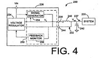
- Figure 4 shows another power distribution system 230 for supplying a regulated output voltage, Vout, to a system 235 such as an electronic system.
- the power distribution system 230 is similar to power distribution system 30 in function with corresponding elements numbered in the range 230-260, except that the power distribution system 230 includes a signal generator 254 instead of the voltage generator 54 and the pull-up resistor 46.
- the signal generator 254 may be any type of high impedance signal generator such as a current generator, and a voltage generator with a series resistor.
- the output impedance of the signal generator may be selected to be sufficiently high to not load down the source of the feedback signal. For example, if the feedback signal is derived from an inductor-capacitor filter such as inductor 240 and capacitor 242 the source impedance of the inductor-capacitor filter is very low, being approximately 0 ohms, therefore the output impedance may be any impedance greater than approximately 10 ohms.
- the signal generator 254 may be any type of source including an alternating current (AC) source and a direct current (DC) source.
- a tone detector may monitor the feedback input of the voltage regulator 234 to detect an AC signal from the AC source, which indicates a degraded electrical condition of the feedback line 232 and feedback terminal 244.
- the feedback monitor 256 may comprise the tone detector.
Landscapes
- Engineering & Computer Science (AREA)
- Power Engineering (AREA)
- Physics & Mathematics (AREA)
- Electromagnetism (AREA)
- General Physics & Mathematics (AREA)
- Radar, Positioning & Navigation (AREA)
- Automation & Control Theory (AREA)
- Dc-Dc Converters (AREA)
- Continuous-Control Power Sources That Use Transistors (AREA)
- Control Of Voltage And Current In General (AREA)
Claims (17)
- Integrierte Schaltung (36), die umfasst:einen Ausgangsanschluss (38);einen Rückkopplungsanschluss (44) zum Empfangen eines Rückkopplungssignals (32);einen Spannungsregler (34) mit einem Rückkopplungseingang zum Empfangen des Rückkopplungssignals von dem Rückkopplungsanschluss;wobei der Spannungsregler (34) einen Leistungsausgang hat, der mit dem Ausgangsanschluss in Verbindung steht, und der Spannungsregler auf das Rückkopplungssignal anspricht, um die Leistung, die an eine Ausgangsspannung ausgegeben wird, zu erzeugen und zu regeln;einen Spannungsgenerator (54) zum Erzeugen einer Pull-up-Spannung, die eine Amplitude hat, die größer ist als eine Gleichspannungsamplitude der Ausgangsspannung, wobei die Pull-up-Spannung separat von dem Leistungsausgang hergeleitet wird; undeinen Pull-up-Wderstand (64), der die Pull-up-Spannung zu dem Rückkopplungseingang des Spannungsreglers koppelt.
- Integrierte Schaltung nach Anspruch 1, wobei die Pull-up-Spannung ungefähr 120 % der Gleichspannungsamplitude des Leistungsausgangs beträgt.
- Integrierte Schaltung nach Anspruch 1, die des weiteren ein Filter zum Erzeugen einer regulierten Ausgangsspannung von dem Leistungsausgang umfasst; und
wobei das Rückkopplungssignal von der geregelten Ausgangsspannung hergeleitet wird. - Integrierte Schaltung nach Anspruch 3, die in einem Stromverteilungssystem integriert ist, das eine Rückkopplungsleitung zum Leiten des Rückkopplungssignals von der regulierten Ausgangsspannung zu dem Rückkopplungsanschluss umfasst.
- Integrierte Schaltung nach Anspruch 1, die in einem Stromverteilungssystem enthalten ist, das externe Filter umfasst, die mit dem Ausgangsanschluss gekoppelt sind;
wobei die externen Filterkomponenten eine Ausgangsinduktivität (40) und einen Ausgangskondensator (42) zum Filtern des Ausgangsstroms umfassen, um eine geregelte Ausgangsspannung zu erzeugen. - Integrierte Schaltung nach Anspruch 1, wobei der Pull-up-Widerstand eine Impedanz im Bereich von ungefähr 100 Ohm bis 1.000.000 Ohm hat.
- Integrierte Schaltung nach Anspruch 1, wobei der Spannungsregler aus einer Gruppe ausgewählt wird, die aus einem Schaltregler und einem Linearregler besteht.
- Integrierte Schaltung nach Anspruch 1, wobei der Ausgangsanschluss aus einer Gruppe ausgewählt wird, die aus einem Stift, einem Ball-Grid-Array und einem Verbinder besteht.
- Integrierte Schaltung nach Anspruch 1, wobei der Rückkopplungsanschluss aus einer Gruppe ausgewählt wird, die aus einem Stift, einem Ball-Grid-Array und einem Verbinder besteht.
- Integrierte Schaltung nach Anspruch 4, die des Weiteren eine Rückkopplungs-Überwachungseinrichtung (56) zum Erfassen einer elektrisch geschwächten Verbindung zwischen dem Rückkopplungsanschluss und der geregelten Ausgangsspannung umfasst.
- Integrierte Schaltung nach Anspruch 10, wobei der Leistungsausgang eine Amplitude hat; und
wobei die elektrisch geschwächte Verbindung dadurch definiert ist, dass sie eine erhöhte Impedanz aufweist, die bewirkt, dass die Qualität des Rückkopplungssignals für den Spannungsregler zum Steuern der Amplitude des Leistungsausgangs nicht ausreicht. - Integrierte Schaltung nach Anspruch 10, wobei die elektrisch geschwächte Verbindung aus einer Gruppe ausgewählt wird, die aus einer kalten Lötstelle, einer teilweisen Trennung der Rückkopplungsleitung von der regulierten Ausgangsspannung und einer vollständigen Trennung der Rückkopplungsleitung von der geregelten Ausgangsspannung besteht.
- Integrierte Schaltung nach Anspruch 10, wobei die Rückkopplungs-Überwachungseinrichtung eine Spannung an dem Rückkopplungsanschluss mit einer Bezugsspannung vergleicht, um die elektrisch geschwächte Verbindung zu erfassen.
- Integrierte Schaltung nach Anspruch 1, wobei die integrierte Schaltung des Weiteren wenigstens zwei Rückkopplungsanschlüsse umfasst, die jeweils das Rückkopplungssignal empfangen.
- Integrierte Schaltung nach Anspruch 14, die in einem Stromverteilungssystem enthalten ist, das umfasst:ein Filter zum Erzeugen einer geregelten Ausgangsspannung von dem Leistungsausgang; undredundante Rückkopplungsleitungen, die zwischen die geregelte Ausgangsspannung und die wenigstens zwei Rückkopplungsanschlüsse der integrierten Schaltung gekoppelt sind, um das Rückkopplungssignal zu leiten.
- Integrierte Schaltung nach Anspruch 14, die des Weiteren eine Verbindungsschaltung zum Verbinden der Rückkopplungsanschlüsse miteinander umfasst.
- Integrierte Schaltung nach Anspruch 1, wobei der Spannungsgenerator ein Quellentyp ist, der aus einer Gruppe ausgewählt wird, die aus einer Wechselstromquelle und einer Gleichstromquelle besteht.
Priority Applications (2)
| Application Number | Priority Date | Filing Date | Title |
|---|---|---|---|
| EP05011612A EP1602997B1 (de) | 2004-05-13 | 2005-04-18 | Spannungsregler mit Signalgenerator mit hoher Ausgangsimpedanz |
| EP05011613A EP1602998A1 (de) | 2004-05-13 | 2005-04-18 | Spannungsregler mit Mehrfach-Rückführung |
Applications Claiming Priority (2)
| Application Number | Priority Date | Filing Date | Title |
|---|---|---|---|
| US846717 | 2004-05-13 | ||
| US10/846,717 US7514911B2 (en) | 2004-05-13 | 2004-05-13 | Voltage regulator feedback protection method and apparatus |
Related Child Applications (2)
| Application Number | Title | Priority Date | Filing Date |
|---|---|---|---|
| EP05011613A Division EP1602998A1 (de) | 2004-05-13 | 2005-04-18 | Spannungsregler mit Mehrfach-Rückführung |
| EP05011612A Division EP1602997B1 (de) | 2004-05-13 | 2005-04-18 | Spannungsregler mit Signalgenerator mit hoher Ausgangsimpedanz |
Publications (2)
| Publication Number | Publication Date |
|---|---|
| EP1596267A1 EP1596267A1 (de) | 2005-11-16 |
| EP1596267B1 true EP1596267B1 (de) | 2008-10-15 |
Family
ID=34935311
Family Applications (3)
| Application Number | Title | Priority Date | Filing Date |
|---|---|---|---|
| EP05011612A Expired - Fee Related EP1602997B1 (de) | 2004-05-13 | 2005-04-18 | Spannungsregler mit Signalgenerator mit hoher Ausgangsimpedanz |
| EP05011613A Ceased EP1602998A1 (de) | 2004-05-13 | 2005-04-18 | Spannungsregler mit Mehrfach-Rückführung |
| EP05008414A Expired - Fee Related EP1596267B1 (de) | 2004-05-13 | 2005-04-18 | Rückkopplungsschutzschaltung und Verfahren für Spannungsregler |
Family Applications Before (2)
| Application Number | Title | Priority Date | Filing Date |
|---|---|---|---|
| EP05011612A Expired - Fee Related EP1602997B1 (de) | 2004-05-13 | 2005-04-18 | Spannungsregler mit Signalgenerator mit hoher Ausgangsimpedanz |
| EP05011613A Ceased EP1602998A1 (de) | 2004-05-13 | 2005-04-18 | Spannungsregler mit Mehrfach-Rückführung |
Country Status (6)
| Country | Link |
|---|---|
| US (2) | US7514911B2 (de) |
| EP (3) | EP1602997B1 (de) |
| JP (3) | JP4712429B2 (de) |
| CN (3) | CN1696859B (de) |
| DE (2) | DE602005019946D1 (de) |
| TW (3) | TWI388963B (de) |
Families Citing this family (9)
| Publication number | Priority date | Publication date | Assignee | Title |
|---|---|---|---|---|
| US8008970B1 (en) | 2010-06-07 | 2011-08-30 | Skyworks Solutions, Inc. | Apparatus and method for enabled switch detection |
| US8988140B2 (en) | 2013-06-28 | 2015-03-24 | International Business Machines Corporation | Real-time adaptive voltage control of logic blocks |
| JP2016181071A (ja) * | 2015-03-24 | 2016-10-13 | 日立オートモティブシステムズ株式会社 | 電源装置 |
| KR102163054B1 (ko) * | 2015-09-15 | 2020-10-08 | 삼성전기주식회사 | 신호 생성 장치 |
| CN107678482B (zh) * | 2017-09-12 | 2020-04-03 | 郑州云海信息技术有限公司 | 一种电压调节的装置及调节方法 |
| DE112018007757T5 (de) * | 2018-06-22 | 2021-03-11 | Rohm Co., Ltd. | Schaltnetzteil, integrierte halbleiterschaltungseinrichtung und differentialeingangsschaltung |
| CN111130328B (zh) * | 2018-10-31 | 2021-12-28 | 瑞昱半导体股份有限公司 | 介面电路以及控制介面电路内的开关电路的方法 |
| CN113994295B (zh) * | 2019-08-15 | 2023-06-02 | 赤多尼科两合股份有限公司 | 输出负载识别方法和结合有该方法的设备 |
| CN114337297A (zh) * | 2021-12-15 | 2022-04-12 | 珠海格力电器股份有限公司 | 一种开关电源的反馈电路、开关电源及用电设备 |
Family Cites Families (33)
| Publication number | Priority date | Publication date | Assignee | Title |
|---|---|---|---|---|
| US3769568A (en) * | 1972-07-31 | 1973-10-30 | Bell Telephone Labor Inc | Dc-to-dc converter having soft start and other regulation features employing priority of pulse feedback |
| US4621313A (en) * | 1985-06-28 | 1986-11-04 | Zenith Electronics Corporation | Soft-start capacitor discharge circuit |
| JPH0331531A (ja) * | 1989-06-27 | 1991-02-12 | Nissan Motor Co Ltd | 内燃機関のスロットル弁制御装置 |
| IE75374B1 (en) * | 1989-11-13 | 1997-09-10 | Nat Csf Corp | Uninterruptible power supply |
| JPH0655295B2 (ja) | 1990-06-27 | 1994-07-27 | 新日本製鐵株式会社 | 耐食性,溶接性,潤滑性,連続パンチ打抜き性,上塗り塗装性に優れた表面処理鋼板及びその製造方法 |
| JP2545533Y2 (ja) * | 1990-10-04 | 1997-08-25 | 株式会社リコー | レーザダイオード制御回路 |
| US5204809A (en) * | 1992-04-03 | 1993-04-20 | International Business Machines Corporation | H-driver DC-to-DC converter utilizing mutual inductance |
| US5408173A (en) * | 1992-10-01 | 1995-04-18 | Kronos Incorporated | Manual-adjustment-free controlled-voltage and current-limited D.C. voltage supply |
| JP3426342B2 (ja) * | 1994-06-03 | 2003-07-14 | 日本アビオニクス株式会社 | 溶接電源 |
| US5530636A (en) | 1995-01-13 | 1996-06-25 | Dell Usa, L.P. | Automatic feedback system for a dual output power supply |
| US5508603A (en) * | 1995-03-28 | 1996-04-16 | Northrop Grumman Corporation | Polarity corrected, intermittent compensated, remote load voltage regulation |
| JP3349897B2 (ja) * | 1995-08-11 | 2002-11-25 | 富士通株式会社 | 直流−直流変換装置 |
| US6046896A (en) | 1995-08-11 | 2000-04-04 | Fijitsu Limited | DC-to-DC converter capable of preventing overvoltage |
| JPH0984342A (ja) * | 1995-09-18 | 1997-03-28 | Ricoh Co Ltd | 電源装置 |
| US5672958A (en) * | 1995-11-14 | 1997-09-30 | Dell Usa L.P. | Method and apparatus for modifying feedback sensing for a redundant power supply system |
| US5698973A (en) | 1996-07-31 | 1997-12-16 | Data General Corporation | Soft-start switch with voltage regulation and current limiting |
| US5894243A (en) * | 1996-12-11 | 1999-04-13 | Micro Linear Corporation | Three-pin buck and four-pin boost converter having open loop output voltage control |
| SE520359C2 (sv) * | 1997-03-06 | 2003-07-01 | Ericsson Telefon Ab L M | Elektrisk krets för att kompensera oönskat spänningsbortfall i en ledare |
| JPH10248252A (ja) * | 1997-03-07 | 1998-09-14 | Meidensha Corp | コンデンサの充電装置 |
| SE509679C2 (sv) * | 1997-04-10 | 1999-02-22 | Ericsson Telefon Ab L M | Förfarande för att styra en likspänning från en DC-DC- omvandlare och en DC-DC-omvandlare |
| US5834925A (en) * | 1997-05-08 | 1998-11-10 | Cisco Technology, Inc. | Current sharing power supplies with redundant operation |
| US5867013A (en) * | 1997-11-20 | 1999-02-02 | Cypress Semiconductor Corporation | Startup circuit for band-gap reference circuit |
| JPH11249750A (ja) * | 1998-03-02 | 1999-09-17 | Minolta Co Ltd | 電子機器 |
| US5977757A (en) * | 1998-11-02 | 1999-11-02 | Hewlett-Packard Company | Power supply having automatic voltage sensing |
| US6301133B1 (en) * | 1999-04-07 | 2001-10-09 | Astec International Limited | Power supply system with ORing element and control circuit |
| CN1312493A (zh) * | 2000-02-07 | 2001-09-12 | 精工电子有限公司 | 半导体集成电路 |
| JP2001359273A (ja) * | 2000-06-14 | 2001-12-26 | Toshiba Corp | 電源装置及びこの電源装置を有する情報処理装置 |
| US6362986B1 (en) * | 2001-03-22 | 2002-03-26 | Volterra, Inc. | Voltage converter with coupled inductive windings, and associated methods |
| JP3595532B2 (ja) | 2001-10-18 | 2004-12-02 | Smk株式会社 | 半導体レーザの駆動制御装置 |
| US6958552B2 (en) * | 2002-04-10 | 2005-10-25 | Adc Dsl Systems, Inc. | Failsafe power oring with current sharing |
| CN2553414Y (zh) * | 2002-07-05 | 2003-05-28 | 北京通力环电气股份有限公司 | Pwm型高频开关电源恒压/恒流控制器 |
| US6772011B2 (en) * | 2002-08-20 | 2004-08-03 | Thoratec Corporation | Transmission of information from an implanted medical device |
| KR100594872B1 (ko) | 2002-10-04 | 2006-06-30 | 롬 씨오.엘티디 | 전압귀환회로를 갖는 반도체 장치 및 이를 이용한 전자장치 |
-
2004
- 2004-05-13 US US10/846,717 patent/US7514911B2/en active Active
-
2005
- 2005-04-18 EP EP05011612A patent/EP1602997B1/de not_active Expired - Fee Related
- 2005-04-18 DE DE602005019946T patent/DE602005019946D1/de active Active
- 2005-04-18 EP EP05011613A patent/EP1602998A1/de not_active Ceased
- 2005-04-18 DE DE602005010325T patent/DE602005010325D1/de active Active
- 2005-04-18 EP EP05008414A patent/EP1596267B1/de not_active Expired - Fee Related
- 2005-04-20 TW TW094112632A patent/TWI388963B/zh not_active IP Right Cessation
- 2005-04-20 TW TW094132733A patent/TWI370341B/zh not_active IP Right Cessation
- 2005-04-20 TW TW094132734A patent/TW200613942A/zh unknown
- 2005-04-25 JP JP2005126973A patent/JP4712429B2/ja not_active Expired - Fee Related
- 2005-04-29 CN CN200510067954.5A patent/CN1696859B/zh not_active Expired - Fee Related
- 2005-05-13 CN CN200510069369.9A patent/CN1702587B/zh not_active Expired - Fee Related
- 2005-05-13 CN CNA2005100752254A patent/CN1862437A/zh active Pending
- 2005-06-20 JP JP2005180009A patent/JP4712453B2/ja not_active Expired - Fee Related
- 2005-06-20 JP JP2005180008A patent/JP2006014590A/ja not_active Withdrawn
-
2009
- 2009-03-05 US US12/398,265 patent/US7960958B2/en not_active Expired - Lifetime
Also Published As
| Publication number | Publication date |
|---|---|
| TWI388963B (zh) | 2013-03-11 |
| CN1696859A (zh) | 2005-11-16 |
| CN1696859B (zh) | 2010-06-02 |
| CN1702587B (zh) | 2010-04-14 |
| EP1602997A1 (de) | 2005-12-07 |
| JP2006014590A (ja) | 2006-01-12 |
| JP2005327270A (ja) | 2005-11-24 |
| TW200613942A (en) | 2006-05-01 |
| US20090167275A1 (en) | 2009-07-02 |
| JP4712429B2 (ja) | 2011-06-29 |
| TW200537268A (en) | 2005-11-16 |
| US20050253566A1 (en) | 2005-11-17 |
| US7960958B2 (en) | 2011-06-14 |
| TW200602833A (en) | 2006-01-16 |
| JP2005354896A (ja) | 2005-12-22 |
| EP1602998A1 (de) | 2005-12-07 |
| DE602005019946D1 (de) | 2010-04-29 |
| EP1596267A1 (de) | 2005-11-16 |
| DE602005010325D1 (de) | 2008-11-27 |
| CN1702587A (zh) | 2005-11-30 |
| EP1602997B1 (de) | 2010-03-17 |
| TWI370341B (en) | 2012-08-11 |
| US7514911B2 (en) | 2009-04-07 |
| JP4712453B2 (ja) | 2011-06-29 |
| CN1862437A (zh) | 2006-11-15 |
Similar Documents
| Publication | Publication Date | Title |
|---|---|---|
| EP1596267B1 (de) | Rückkopplungsschutzschaltung und Verfahren für Spannungsregler | |
| US9866016B2 (en) | Multiport power converter with load detection capabilities | |
| US6301133B1 (en) | Power supply system with ORing element and control circuit | |
| US5737204A (en) | Method and apparatus for interfacing battery backup to power factor correction front end for maintaining power | |
| JP2667345B2 (ja) | N+1電力供給システム | |
| US8710820B2 (en) | Switched capacitor hold-up scheme for constant boost output voltage | |
| CN1909314B (zh) | 装备有电源电路的电子断开装置和包含断开装置的断路器 | |
| US20040062063A1 (en) | Dynamic DC source and load energy recycling power system | |
| KR20090045917A (ko) | 전자 시스템, 전자장치 및 전원장치 | |
| JP7151574B2 (ja) | 電源システム及び電源装置 | |
| EP1224720B1 (de) | Vereinfachte stromaufteilungsschaltung | |
| Schuellein | Current sharing of redundant synchronous buck regulators powering high performance microprocessors using the V/sup 2/control method | |
| EP1107417A2 (de) | Schaltung und Verfahren zur Erzeugung abgeschätzter Rückkopplung für den Regler eines Slave-Stromversorgungsmoduls in einer Master-Slave Parallelanordnung | |
| CN216115893U (zh) | 扫描仪及扫描系统 | |
| CN111009958B (zh) | 一种供电控制电路 | |
| US20240120765A1 (en) | Integrated battery charge regulation circuit based on power fet conductivity modulation | |
| TWI441432B (zh) | 開關機電壓設定與輸出功率補償之整合控制電路及其操作方法 | |
| KR100419740B1 (ko) | 경보발생을 방지하는 보상회로를 포함하는 전원 모듈이병렬로 접속된 전원 공급 장치 | |
| US20090033409A1 (en) | Bias correction device | |
| Angkititrakul et al. | Design considerations of 1.2 kW redundant parallel DC/DC power supplies | |
| CN114337190A (zh) | 一种输出电压补偿电路及补偿方法 | |
| JPH11252906A (ja) | 電源活性保守化アダプタ | |
| JPH08115133A (ja) | 電源装置 | |
| KR20030012346A (ko) | 스위칭방식 전원의 출력 정전압 체크장치 | |
| KR20050117724A (ko) | 이상 동작 방지 기능을 구비한 충전 회로 |
Legal Events
| Date | Code | Title | Description |
|---|---|---|---|
| PUAI | Public reference made under article 153(3) epc to a published international application that has entered the european phase |
Free format text: ORIGINAL CODE: 0009012 |
|
| AK | Designated contracting states |
Kind code of ref document: A1 Designated state(s): AT BE BG CH CY CZ DE DK EE ES FI FR GB GR HU IE IS IT LI LT LU MC NL PL PT RO SE SI SK TR |
|
| AX | Request for extension of the european patent |
Extension state: AL BA HR LV MK YU |
|
| 17P | Request for examination filed |
Effective date: 20060512 |
|
| AKX | Designation fees paid |
Designated state(s): DE FR GB |
|
| 17Q | First examination report despatched |
Effective date: 20070220 |
|
| GRAP | Despatch of communication of intention to grant a patent |
Free format text: ORIGINAL CODE: EPIDOSNIGR1 |
|
| GRAS | Grant fee paid |
Free format text: ORIGINAL CODE: EPIDOSNIGR3 |
|
| GRAA | (expected) grant |
Free format text: ORIGINAL CODE: 0009210 |
|
| AK | Designated contracting states |
Kind code of ref document: B1 Designated state(s): DE FR GB |
|
| REG | Reference to a national code |
Ref country code: GB Ref legal event code: FG4D |
|
| REF | Corresponds to: |
Ref document number: 602005010325 Country of ref document: DE Date of ref document: 20081127 Kind code of ref document: P |
|
| PLBE | No opposition filed within time limit |
Free format text: ORIGINAL CODE: 0009261 |
|
| STAA | Information on the status of an ep patent application or granted ep patent |
Free format text: STATUS: NO OPPOSITION FILED WITHIN TIME LIMIT |
|
| 26N | No opposition filed |
Effective date: 20090716 |
|
| REG | Reference to a national code |
Ref country code: FR Ref legal event code: PLFP Year of fee payment: 12 |
|
| REG | Reference to a national code |
Ref country code: FR Ref legal event code: PLFP Year of fee payment: 13 |
|
| REG | Reference to a national code |
Ref country code: FR Ref legal event code: PLFP Year of fee payment: 14 |
|
| PGFP | Annual fee paid to national office [announced via postgrant information from national office to epo] |
Ref country code: DE Payment date: 20180427 Year of fee payment: 14 |
|
| PGFP | Annual fee paid to national office [announced via postgrant information from national office to epo] |
Ref country code: FR Payment date: 20180425 Year of fee payment: 14 |
|
| PGFP | Annual fee paid to national office [announced via postgrant information from national office to epo] |
Ref country code: GB Payment date: 20180427 Year of fee payment: 14 |
|
| REG | Reference to a national code |
Ref country code: DE Ref legal event code: R119 Ref document number: 602005010325 Country of ref document: DE |
|
| GBPC | Gb: european patent ceased through non-payment of renewal fee |
Effective date: 20190418 |
|
| PG25 | Lapsed in a contracting state [announced via postgrant information from national office to epo] |
Ref country code: GB Free format text: LAPSE BECAUSE OF NON-PAYMENT OF DUE FEES Effective date: 20190418 Ref country code: DE Free format text: LAPSE BECAUSE OF NON-PAYMENT OF DUE FEES Effective date: 20191101 |
|
| PG25 | Lapsed in a contracting state [announced via postgrant information from national office to epo] |
Ref country code: FR Free format text: LAPSE BECAUSE OF NON-PAYMENT OF DUE FEES Effective date: 20190430 |