EP1596212B1 - Work function controlled probe for measuring properties of a semiconductor wafer and method of use thereof - Google Patents
Work function controlled probe for measuring properties of a semiconductor wafer and method of use thereof Download PDFInfo
- Publication number
- EP1596212B1 EP1596212B1 EP05104011A EP05104011A EP1596212B1 EP 1596212 B1 EP1596212 B1 EP 1596212B1 EP 05104011 A EP05104011 A EP 05104011A EP 05104011 A EP05104011 A EP 05104011A EP 1596212 B1 EP1596212 B1 EP 1596212B1
- Authority
- EP
- European Patent Office
- Prior art keywords
- contact
- work function
- semiconductor wafer
- coating
- electrical
- Prior art date
- Legal status (The legal status is an assumption and is not a legal conclusion. Google has not performed a legal analysis and makes no representation as to the accuracy of the status listed.)
- Expired - Lifetime
Links
- 239000004065 semiconductor Substances 0.000 title claims abstract description 33
- 238000000034 method Methods 0.000 title claims abstract description 16
- 239000000523 sample Substances 0.000 title claims description 10
- 239000000463 material Substances 0.000 claims abstract description 49
- 238000000576 coating method Methods 0.000 claims abstract description 40
- 239000011248 coating agent Substances 0.000 claims abstract description 37
- 239000012799 electrically-conductive coating Substances 0.000 claims abstract description 3
- 229910052715 tantalum Inorganic materials 0.000 claims description 9
- GUVRBAGPIYLISA-UHFFFAOYSA-N tantalum atom Chemical compound [Ta] GUVRBAGPIYLISA-UHFFFAOYSA-N 0.000 claims description 9
- 229910052741 iridium Inorganic materials 0.000 claims description 7
- GKOZUEZYRPOHIO-UHFFFAOYSA-N iridium atom Chemical compound [Ir] GKOZUEZYRPOHIO-UHFFFAOYSA-N 0.000 claims description 7
- KJTLSVCANCCWHF-UHFFFAOYSA-N Ruthenium Chemical compound [Ru] KJTLSVCANCCWHF-UHFFFAOYSA-N 0.000 claims description 3
- 229910052707 ruthenium Inorganic materials 0.000 claims description 3
- 229910052751 metal Inorganic materials 0.000 claims description 2
- 239000002184 metal Substances 0.000 claims description 2
- 150000002739 metals Chemical class 0.000 claims description 2
- 235000012431 wafers Nutrition 0.000 description 21
- 239000000758 substrate Substances 0.000 description 12
- 238000012360 testing method Methods 0.000 description 12
- 238000005259 measurement Methods 0.000 description 6
- BASFCYQUMIYNBI-UHFFFAOYSA-N platinum Chemical compound [Pt] BASFCYQUMIYNBI-UHFFFAOYSA-N 0.000 description 4
- 229910001362 Ta alloys Inorganic materials 0.000 description 2
- 230000004075 alteration Effects 0.000 description 2
- 238000012986 modification Methods 0.000 description 2
- 230000004048 modification Effects 0.000 description 2
- 229910052697 platinum Inorganic materials 0.000 description 2
- 229910000575 Ir alloy Inorganic materials 0.000 description 1
- 238000004630 atomic force microscopy Methods 0.000 description 1
- 239000002800 charge carrier Substances 0.000 description 1
- 239000004020 conductor Substances 0.000 description 1
- 230000001419 dependent effect Effects 0.000 description 1
- 238000010586 diagram Methods 0.000 description 1
- 238000004519 manufacturing process Methods 0.000 description 1
- 230000000873 masking effect Effects 0.000 description 1
- 238000004621 scanning probe microscopy Methods 0.000 description 1
- 230000005641 tunneling Effects 0.000 description 1
Images

Classifications
-
- G—PHYSICS
- G01—MEASURING; TESTING
- G01R—MEASURING ELECTRIC VARIABLES; MEASURING MAGNETIC VARIABLES
- G01R31/00—Arrangements for testing electric properties; Arrangements for locating electric faults; Arrangements for electrical testing characterised by what is being tested not provided for elsewhere
- G01R31/26—Testing of individual semiconductor devices
- G01R31/2648—Characterising semiconductor materials
-
- G—PHYSICS
- G01—MEASURING; TESTING
- G01R—MEASURING ELECTRIC VARIABLES; MEASURING MAGNETIC VARIABLES
- G01R1/00—Details of instruments or arrangements of the types included in groups G01R5/00 - G01R13/00 and G01R31/00
- G01R1/02—General constructional details
- G01R1/06—Measuring leads; Measuring probes
- G01R1/067—Measuring probes
- G01R1/06711—Probe needles; Cantilever beams; "Bump" contacts; Replaceable probe pins
Definitions
- the present invention relates to testing of semiconductor wafers.
- conductive elastic probes for measuring one or more electrical properties of a semiconductor wafer is disclosed in United States Patent No. 6,492,827 to Mazur et al. It has been observed that conductive elastic probes formed from certain materials, such as platinum, iridium or tantalum, or probes having platinum, iridium or tantalum-coated tips work best for testing semiconductor wafers. Heretofore, it was believed that the inability to grow oxides and/or the ability to grow conductive oxides on one or more of these materials rendered them more useful for such testing. However, in accordance with the present invention, it is believed that the work function of the probe surface that presses into contact with a semiconductor wafer during the testing can affect the measurement thereof.
- EP-A-1 413 892 discloses a method and apparatus for measuring charge carrier lifetime of a semiconductor wafer.
- US-A-6,139,759 discloses a method of manufacturing silicided microtips for scanning probe microscopy.
- US-A-2004/0016286 discloses atomic force microscopy measurements of contact resistance and current-dependent stiction. It describes electron tunneling theory using a work function that assumes a variation of the work function with applied force (on the tip). Data were computed for a fixed work function value and a fixed film thickness.
- the invention is a method as defined is claim 1.
- the conductive contact can be the tip of a probe.
- the coating can have a thickness of an extent whereupon the conductive contact has an overall work function that is either equal to the second work function or intermediate the first work function and the second work function. Desirably, the thickness of the coating is no more than five (5) Debye lengths.
- the base material can be comprised of tantalum and the coating can be comprised of iridium.
- the coating can include a layer of first material overlaying the base material and a layer of a second material overlaying the first material, wherein the second work function is related to, e.g., intermediate, the work functions of the first and second materials.
- the base material, the first material and the second material are different metals.
- the base material can be comprised of tantalum
- the first material can be comprised of iridium
- the second material can be comprised of at least one of a ruthenium and tantalum.
- Fig. 1 is a cross-sectional view of a semiconductor wafer having a block diagram of a semiconductor wafer test system in operative relation thereto;
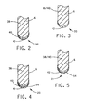
- Figs. 2-5 are different embodiments of a contact of the test system shown in Fig. 1 .
- a semiconductor wafer test system 2 includes an electrically conductive vacuum chuck 4 and a contact 6.
- the illustration of contact 6 in Fig. 1 in the form of an elongated probe is not to be construed as limiting the invention since it is envisioned that contact 6 can have any shape or form suitable for testing a semiconductor wafer 10.
- Chuck 4 is configured to support a backside 8 of a semiconductor wafer 10 which includes a substrate 12 formed of semiconducting material which is held in contact with chuck 4 by means of a vacuum (not shown).
- Semiconductor wafer 10 can, but does not necessarily, include a dielectric layer 14 overlaying a topside 16 of substrate 12.
- contact 6 includes at least a partially spherical and conductive surface 20 for contacting topside 16 of substrate 12 or a topside 22 of dielectric layer 14 when present. While a partially spherical conductive surface 20 is desired, it is envisioned that surfaces (not shown) having other shapes suitable for testing a semiconductor wafer 10 can be utilized. Accordingly, the illustration in Fig. 1 of conductive surface 20 being partially spherical is not to be construed as limiting the invention.
- a contact forming means 26 controls the vertical movement of chuck 4 and/or contact 6, in the directions shown by arrow 28, to move contact 6 and semiconductor wafer 10 toward each other whereupon contact 6 presses into contact with topside 16 of substrate 12 or topside 22 of dielectric layer 14 if present.
- a means for applying electrical stimulus 30 can be electrically connected to apply a suitable electrical stimulus to contact 6 and semiconductor wafer 10 when it is received on chuck 4 and contact 6 is in contact with semiconductor wafer 10.
- a measurement means 32 can be electrically connected for measuring the response of semiconductor wafer 10 to the test stimulus applied by the means for applying electrical stimulus 30.
- chuck 4 is connected to a reference ground.
- this is not to be construed as limiting the invention since chuck 4 alternatively can be connected to an AC or DC reference bias.
- a first embodiment of contact 6 includes a body 38 formed of a suitable electrically conductive material having an electrically conductive layer or coating 42, formed from iridium or an iridium alloy, overlaying an electrically conductive base material 40, such as tantalum or a tantalum alloy, in contact with body 38.
- a second embodiment of contact 6 includes electrically conductive coating 42 overlaying electrically conductive base material 40 which, in this embodiment, forms body 38 of contact 6.
- another embodiment of contact 6 includes body 38 having coating 42 overlaying base material 40 in contact with body 38 in a manner similar to the embodiment of contact 6 shown in Fig. 2 .
- a layer or coating 54 formed from ruthenium (Ru), tantalum (Ta) or a Ru-Ta alloy, overlays coating 42.
- another embodiment of contact 6 includes body 38 formed from a base material 40 like the embodiment of contact 6 shown in Fig. 3 .
- coating 54 overlays coating 42.
- coating 42 is desirably in electrical contact with body 38 only via base material 40. In other words, coating 42 is desirably not in direct electrical contact with body 38.
- coating 42 is directly in contact with body 38 formed from base material 40.
- coating 42 is desirably in contact with body 38 only via base material 40
- coating 54 is desirably in contact with body 38 only via coating 42 and base material 40. In other words, there is no direct electrical contact between coating 42 and body 38, or between coating 54 and base material 40 or body 38.
- coating 54 is desirably in contact with body 38 only via coating 42. In other words, coating 54 is not in direct electrical contact with body 38 formed from base material 40.
- coating 42 has a thickness whereupon surface 20 of each embodiment contact 6 has an overall work function equal to the work function of the material forming coating 42.
- coating 42 can have a thickness whereupon surface 20 of each embodiment contact 6 has an overall work function that is intermediate the work functions of the materials forming coating 42 and base material 40.
- coating 42 must be thick enough to impart the work function of its material to the overall work function, but thin enough to avoid its work function from masking the work function of base material 40.
- coating 42 has a thickness of no more than five (5) Debye lengths. However, this is not to be construed as limiting the invention.
- coating 54 desirably has a thickness whereupon surface 20 has an overall work function that is either equal to the work function of the material forming coating 54 or a work function intermediate the work functions of coatings 42 and 54. This intermediate work function can be achieved by controlling the thickness of coating 54 in the manner described above for coating 42 overlaying base material 40.
- the work function of surface 20 of each of the embodiments of contact 6 shown in Figs. 2-5 is between 3.0 eV and 6.0 eV for testing semiconductor wafers.
- this is not to be construed as limiting the invention since the overall work function of surface 20 can be set as desired to optimize the testing of semiconductor wafers.
- contact forming means 26 causes surface 20 of contact 6 to press into contact with either topside surface 16 of substrate 12 or topside 22 of dielectric layer 14 if provided, thereby forming a first electrical contact.
- the backside 8 of semiconductor wafer 10 in contact with chuck 4 defines a second electrical contact.
- the second electrical contact can be formed directly with substrate 12 or via another contact (not shown) in contact with topside surface 16 of substrate 12 or topside 22 of dielectric layer 14 if provided.
- the means for applying the electrical stimulus 30 applies a suitable electrical stimulus between the first electrical contact and the second electrical contact.
- measurement means 32 measures a response of the semiconductor wafer 10 to the electric stimulus. Based on this response, measurement means 32 can determine at least one electrical property of dielectric layer 14, substrate 12, an interface of dielectric layer 14 and substrate 12, or some combination thereof.
- Non-limiting examples of suitable electrical stimuli that can be applied by the means for applying electrical stimulus 30 that measurement means 32 can measure include a capacitance-voltage type stimulus (CV), a conductance-voltage (GV) type stimulus, a charge-voltage (QV) type stimulus, and/or a current-voltage (IV) type stimulus.
- Non-limiting examples of electrical properties that can be determined from these stimuli include flat-band voltage (V FB ), threshold voltage (V T ) and leakage current (I LEAK ).
- each of the embodiments of contact 6 is illustrated as a probe having a tip defining surface 20.
- this is not to be construed as limiting the invention.
- the illustration of the various layers 40, 42, 54 extending outside the radius of body 38 is shown for illustration purposes only.
- coatings 40, 42, and 54 are relatively thin whereupon these layers would not extend outside the radius of body 38 to the extent shown in Figs. 2-5 . It is intended that the invention be construed as including all such modifications and alterations insofar as they come within the scope of the appended claims.
Landscapes
- Physics & Mathematics (AREA)
- General Physics & Mathematics (AREA)
- Testing Or Measuring Of Semiconductors Or The Like (AREA)
- Measuring Leads Or Probes (AREA)
- Testing Of Individual Semiconductor Devices (AREA)
Applications Claiming Priority (2)
| Application Number | Priority Date | Filing Date | Title |
|---|---|---|---|
| US845815 | 2004-05-14 | ||
| US10/845,815 US7023231B2 (en) | 2004-05-14 | 2004-05-14 | Work function controlled probe for measuring properties of a semiconductor wafer and method of use thereof |
Publications (2)
| Publication Number | Publication Date |
|---|---|
| EP1596212A1 EP1596212A1 (en) | 2005-11-16 |
| EP1596212B1 true EP1596212B1 (en) | 2008-09-10 |
Family
ID=34939824
Family Applications (1)
| Application Number | Title | Priority Date | Filing Date |
|---|---|---|---|
| EP05104011A Expired - Lifetime EP1596212B1 (en) | 2004-05-14 | 2005-05-13 | Work function controlled probe for measuring properties of a semiconductor wafer and method of use thereof |
Country Status (6)
| Country | Link |
|---|---|
| US (1) | US7023231B2 (OSRAM) |
| EP (1) | EP1596212B1 (OSRAM) |
| JP (1) | JP2005333148A (OSRAM) |
| AT (1) | ATE408154T1 (OSRAM) |
| DE (1) | DE602005009603D1 (OSRAM) |
| TW (1) | TWI391686B (OSRAM) |
Families Citing this family (57)
| Publication number | Priority date | Publication date | Assignee | Title |
|---|---|---|---|---|
| US6380751B2 (en) | 1992-06-11 | 2002-04-30 | Cascade Microtech, Inc. | Wafer probe station having environment control enclosure |
| US5345170A (en) | 1992-06-11 | 1994-09-06 | Cascade Microtech, Inc. | Wafer probe station having integrated guarding, Kelvin connection and shielding systems |
| US5561377A (en) | 1995-04-14 | 1996-10-01 | Cascade Microtech, Inc. | System for evaluating probing networks |
| US6232789B1 (en) | 1997-05-28 | 2001-05-15 | Cascade Microtech, Inc. | Probe holder for low current measurements |
| US5729150A (en) * | 1995-12-01 | 1998-03-17 | Cascade Microtech, Inc. | Low-current probe card with reduced triboelectric current generating cables |
| US5914613A (en) | 1996-08-08 | 1999-06-22 | Cascade Microtech, Inc. | Membrane probing system with local contact scrub |
| US6002263A (en) * | 1997-06-06 | 1999-12-14 | Cascade Microtech, Inc. | Probe station having inner and outer shielding |
| US6034533A (en) * | 1997-06-10 | 2000-03-07 | Tervo; Paul A. | Low-current pogo probe card |
| US6256882B1 (en) | 1998-07-14 | 2001-07-10 | Cascade Microtech, Inc. | Membrane probing system |
| US6578264B1 (en) * | 1999-06-04 | 2003-06-17 | Cascade Microtech, Inc. | Method for constructing a membrane probe using a depression |
| US6445202B1 (en) | 1999-06-30 | 2002-09-03 | Cascade Microtech, Inc. | Probe station thermal chuck with shielding for capacitive current |
| US6838890B2 (en) * | 2000-02-25 | 2005-01-04 | Cascade Microtech, Inc. | Membrane probing system |
| US6965226B2 (en) | 2000-09-05 | 2005-11-15 | Cascade Microtech, Inc. | Chuck for holding a device under test |
| US6914423B2 (en) | 2000-09-05 | 2005-07-05 | Cascade Microtech, Inc. | Probe station |
| DE10143173A1 (de) | 2000-12-04 | 2002-06-06 | Cascade Microtech Inc | Wafersonde |
| US7355420B2 (en) | 2001-08-21 | 2008-04-08 | Cascade Microtech, Inc. | Membrane probing system |
| WO2003020467A1 (en) | 2001-08-31 | 2003-03-13 | Cascade Microtech, Inc. | Optical testing device |
| US6777964B2 (en) | 2002-01-25 | 2004-08-17 | Cascade Microtech, Inc. | Probe station |
| US6951846B2 (en) * | 2002-03-07 | 2005-10-04 | The United States Of America As Represented By The Secretary Of The Army | Artemisinins with improved stability and bioavailability for therapeutic drug development and application |
| JP2005527823A (ja) | 2002-05-23 | 2005-09-15 | カスケード マイクロテック インコーポレイテッド | デバイスのテスト用プローブ |
| US6847219B1 (en) | 2002-11-08 | 2005-01-25 | Cascade Microtech, Inc. | Probe station with low noise characteristics |
| US6724205B1 (en) | 2002-11-13 | 2004-04-20 | Cascade Microtech, Inc. | Probe for combined signals |
| US7250779B2 (en) | 2002-11-25 | 2007-07-31 | Cascade Microtech, Inc. | Probe station with low inductance path |
| US6861856B2 (en) | 2002-12-13 | 2005-03-01 | Cascade Microtech, Inc. | Guarded tub enclosure |
| US7221172B2 (en) | 2003-05-06 | 2007-05-22 | Cascade Microtech, Inc. | Switched suspended conductor and connection |
| US7492172B2 (en) | 2003-05-23 | 2009-02-17 | Cascade Microtech, Inc. | Chuck for holding a device under test |
| US7057404B2 (en) | 2003-05-23 | 2006-06-06 | Sharp Laboratories Of America, Inc. | Shielded probe for testing a device under test |
| WO2006017078A2 (en) | 2004-07-07 | 2006-02-16 | Cascade Microtech, Inc. | Probe head having a membrane suspended probe |
| US7250626B2 (en) | 2003-10-22 | 2007-07-31 | Cascade Microtech, Inc. | Probe testing structure |
| US7321234B2 (en) * | 2003-12-18 | 2008-01-22 | Lecroy Corporation | Resistive test probe tips and applications therefor |
| WO2005065258A2 (en) | 2003-12-24 | 2005-07-21 | Cascade Microtech, Inc. | Active wafer probe |
| US7187188B2 (en) | 2003-12-24 | 2007-03-06 | Cascade Microtech, Inc. | Chuck with integrated wafer support |
| US7176705B2 (en) | 2004-06-07 | 2007-02-13 | Cascade Microtech, Inc. | Thermal optical chuck |
| US7330041B2 (en) | 2004-06-14 | 2008-02-12 | Cascade Microtech, Inc. | Localizing a temperature of a device for testing |
| KR20070058522A (ko) | 2004-09-13 | 2007-06-08 | 캐스케이드 마이크로테크 인코포레이티드 | 양측 프루빙 구조 |
| US7535247B2 (en) | 2005-01-31 | 2009-05-19 | Cascade Microtech, Inc. | Interface for testing semiconductors |
| US7656172B2 (en) | 2005-01-31 | 2010-02-02 | Cascade Microtech, Inc. | System for testing semiconductors |
| US7282941B2 (en) * | 2005-04-05 | 2007-10-16 | Solid State Measurements, Inc. | Method of measuring semiconductor wafers with an oxide enhanced probe |
| US7449899B2 (en) | 2005-06-08 | 2008-11-11 | Cascade Microtech, Inc. | Probe for high frequency signals |
| US20070294047A1 (en) * | 2005-06-11 | 2007-12-20 | Leonard Hayden | Calibration system |
| EP1932003A2 (en) | 2005-06-13 | 2008-06-18 | Cascade Microtech, Inc. | Wideband active-passive differential signal probe |
| US7637009B2 (en) * | 2006-02-27 | 2009-12-29 | Sv Probe Pte. Ltd. | Approach for fabricating probe elements for probe card assemblies using a reusable substrate |
| DE112007001399T5 (de) | 2006-06-09 | 2009-05-07 | Cascade Microtech, Inc., Beaverton | Messfühler für differentielle Signale mit integrierter Symmetrieschaltung |
| US7723999B2 (en) | 2006-06-12 | 2010-05-25 | Cascade Microtech, Inc. | Calibration structures for differential signal probing |
| US7403028B2 (en) | 2006-06-12 | 2008-07-22 | Cascade Microtech, Inc. | Test structure and probe for differential signals |
| US7764072B2 (en) | 2006-06-12 | 2010-07-27 | Cascade Microtech, Inc. | Differential signal probing system |
| US7443186B2 (en) | 2006-06-12 | 2008-10-28 | Cascade Microtech, Inc. | On-wafer test structures for differential signals |
| US20080290889A1 (en) * | 2007-05-24 | 2008-11-27 | Solid State Measurements, Inc. | Method of destructive testing the dielectric layer of a semiconductor wafer or sample |
| US7876114B2 (en) | 2007-08-08 | 2011-01-25 | Cascade Microtech, Inc. | Differential waveguide probe |
| JP5053788B2 (ja) * | 2007-10-10 | 2012-10-17 | 株式会社アルバック | 導電性プローブ、導電性プローブの製造方法、及び磁気特性測定方法 |
| US7888957B2 (en) | 2008-10-06 | 2011-02-15 | Cascade Microtech, Inc. | Probing apparatus with impedance optimized interface |
| WO2010059247A2 (en) | 2008-11-21 | 2010-05-27 | Cascade Microtech, Inc. | Replaceable coupon for a probing apparatus |
| US8319503B2 (en) | 2008-11-24 | 2012-11-27 | Cascade Microtech, Inc. | Test apparatus for measuring a characteristic of a device under test |
| DE102012205352B4 (de) * | 2012-02-24 | 2022-12-08 | Rohde & Schwarz GmbH & Co. Kommanditgesellschaft | Adapter für einen Tastkopf zur Messung eines differenziellen Signals |
| JP6301680B2 (ja) * | 2014-02-25 | 2018-03-28 | エイブリック株式会社 | 弾性プローブ |
| US20200233033A1 (en) * | 2019-01-17 | 2020-07-23 | Intel Corporation | Test probe for wafer-level and panel-level testing |
| US12411155B2 (en) | 2019-01-29 | 2025-09-09 | Yokowo Co., Ltd. | Plunger and contact probe |
Family Cites Families (20)
| Publication number | Priority date | Publication date | Assignee | Title |
|---|---|---|---|---|
| US4463060A (en) * | 1983-11-15 | 1984-07-31 | E. I. Du Pont De Nemours And Company | Solderable palladium-nickel coatings and method of making said coatings |
| US5378971A (en) * | 1990-11-30 | 1995-01-03 | Tokyo Electron Limited | Probe and a method of manufacturing the same |
| JP2917674B2 (ja) * | 1992-06-03 | 1999-07-12 | 松下電器産業株式会社 | 走査トンネル顕微鏡用探針およびその製造方法 |
| JP2900764B2 (ja) * | 1993-08-30 | 1999-06-02 | 住友金属工業株式会社 | 半導体表面薄膜の評価方法 |
| US5500607A (en) * | 1993-12-22 | 1996-03-19 | International Business Machines Corporation | Probe-oxide-semiconductor method and apparatus for measuring oxide charge on a semiconductor wafer |
| JPH10185878A (ja) * | 1996-12-26 | 1998-07-14 | Mitsubishi Electric Corp | 絶縁破壊測定方法 |
| US5796121A (en) * | 1997-03-25 | 1998-08-18 | International Business Machines Corporation | Thin film transistors fabricated on plastic substrates |
| US6139759A (en) * | 1997-07-08 | 2000-10-31 | International Business Machines Corporation | Method of manufacturing silicided silicon microtips for scanning probe microscopy |
| US6891360B1 (en) * | 1997-10-02 | 2005-05-10 | International Business Machines Corporation | Plated probe structure |
| US6181144B1 (en) * | 1998-02-25 | 2001-01-30 | Micron Technology, Inc. | Semiconductor probe card having resistance measuring circuitry and method fabrication |
| EP1256006B1 (en) * | 1999-10-19 | 2006-07-19 | Solid State Measurements, Inc. | Non-invasive electrical measurement of semiconductor wafers |
| US6741093B2 (en) * | 2000-10-19 | 2004-05-25 | Solid State Measurements, Inc. | Method of determining one or more properties of a semiconductor wafer |
| JP2002131334A (ja) * | 2000-10-24 | 2002-05-09 | Nec Yamaguchi Ltd | プローブ針、プローブカード、及びプローブカードの作製方法 |
| JP2006508495A (ja) * | 2002-03-18 | 2006-03-09 | ナノネクサス インク | 小型化されたコンタクトスプリング |
| US6842029B2 (en) * | 2002-04-11 | 2005-01-11 | Solid State Measurements, Inc. | Non-invasive electrical measurement of semiconductor wafers |
| US6894519B2 (en) * | 2002-04-11 | 2005-05-17 | Solid State Measurements, Inc. | Apparatus and method for determining electrical properties of a semiconductor wafer |
| US6632691B1 (en) * | 2002-04-11 | 2003-10-14 | Solid State Measurements, Inc. | Apparatus and method for determining doping concentration of a semiconductor wafer |
| US6612161B1 (en) * | 2002-07-23 | 2003-09-02 | Fidelica Microsystems, Inc. | Atomic force microscopy measurements of contact resistance and current-dependent stiction |
| US6836139B2 (en) * | 2002-10-22 | 2004-12-28 | Solid State Measurments, Inc. | Method and apparatus for determining defect and impurity concentration in semiconducting material of a semiconductor wafer |
| US6879176B1 (en) * | 2003-11-04 | 2005-04-12 | Solid State Measurements, Inc. | Conductance-voltage (GV) based method for determining leakage current in dielectrics |
-
2004
- 2004-05-14 US US10/845,815 patent/US7023231B2/en not_active Expired - Fee Related
-
2005
- 2005-05-11 TW TW094115310A patent/TWI391686B/zh not_active IP Right Cessation
- 2005-05-13 AT AT05104011T patent/ATE408154T1/de not_active IP Right Cessation
- 2005-05-13 DE DE602005009603T patent/DE602005009603D1/de not_active Expired - Fee Related
- 2005-05-13 JP JP2005170117A patent/JP2005333148A/ja active Pending
- 2005-05-13 EP EP05104011A patent/EP1596212B1/en not_active Expired - Lifetime
Also Published As
| Publication number | Publication date |
|---|---|
| EP1596212A1 (en) | 2005-11-16 |
| DE602005009603D1 (de) | 2008-10-23 |
| ATE408154T1 (de) | 2008-09-15 |
| JP2005333148A (ja) | 2005-12-02 |
| US20050253618A1 (en) | 2005-11-17 |
| US7023231B2 (en) | 2006-04-04 |
| TW200538748A (en) | 2005-12-01 |
| TWI391686B (zh) | 2013-04-01 |
Similar Documents
| Publication | Publication Date | Title |
|---|---|---|
| EP1596212B1 (en) | Work function controlled probe for measuring properties of a semiconductor wafer and method of use thereof | |
| JP4102068B2 (ja) | 測定装置及び電気特性測定方法 | |
| US6842029B2 (en) | Non-invasive electrical measurement of semiconductor wafers | |
| US20040251923A1 (en) | Flexible membrane probe and method of use thereof | |
| US5023561A (en) | Apparatus and method for non-invasive measurement of electrical properties of a dielectric layer in a semiconductor wafer | |
| EP0660387A2 (en) | Method and apparatus for measuring oxide charge on a semiconductor wafer | |
| US6930502B2 (en) | Method using conductive atomic force microscopy to measure contact leakage current | |
| KR100680440B1 (ko) | 절연막의 평가방법 및 평가장치 | |
| EP1584932A1 (en) | Method of testing semiconductor wafers with non-penetrating probes | |
| EP1710594B1 (en) | Method of measuring semiconductor wafers with an oxide enhanced probe | |
| JP2005183933A (ja) | シリコンオンインシュレータ(soi)ウエハの電気特性決定方法 | |
| US20080290889A1 (en) | Method of destructive testing the dielectric layer of a semiconductor wafer or sample | |
| US7190186B2 (en) | Method and apparatus for determining concentration of defects and/or impurities in a semiconductor wafer | |
| JP4623807B2 (ja) | 半導体素子の電圧計測装置および電圧計測方法 | |
| CN119715685B (zh) | 一种测定薄膜功函数的方法 | |
| EP1530053B1 (en) | Conductance-voltage (GV) based method for determining leakage current in dielectrics | |
| US7037734B2 (en) | Method and apparatus for determining generation lifetime of product semiconductor wafers | |
| JP2751353B2 (ja) | ウェハ特性の電気的測定方法および装置 | |
| WO2017147395A1 (en) | High range and resolution scanning probe and methods |
Legal Events
| Date | Code | Title | Description |
|---|---|---|---|
| PUAI | Public reference made under article 153(3) epc to a published international application that has entered the european phase |
Free format text: ORIGINAL CODE: 0009012 |
|
| AK | Designated contracting states |
Kind code of ref document: A1 Designated state(s): AT BE BG CH CY CZ DE DK EE ES FI FR GB GR HU IE IS IT LI LT LU MC NL PL PT RO SE SI SK TR |
|
| AX | Request for extension of the european patent |
Extension state: AL BA HR LV MK YU |
|
| 17P | Request for examination filed |
Effective date: 20060509 |
|
| AKX | Designation fees paid |
Designated state(s): AT BE BG CH CY CZ DE DK EE ES FI FR GB GR HU IE IS IT LI LT LU MC NL PL PT RO SE SI SK TR |
|
| 17Q | First examination report despatched |
Effective date: 20060623 |
|
| 17Q | First examination report despatched |
Effective date: 20060623 |
|
| GRAP | Despatch of communication of intention to grant a patent |
Free format text: ORIGINAL CODE: EPIDOSNIGR1 |
|
| GRAS | Grant fee paid |
Free format text: ORIGINAL CODE: EPIDOSNIGR3 |
|
| GRAA | (expected) grant |
Free format text: ORIGINAL CODE: 0009210 |
|
| AK | Designated contracting states |
Kind code of ref document: B1 Designated state(s): AT BE BG CH CY CZ DE DK EE ES FI FR GB GR HU IE IS IT LI LT LU MC NL PL PT RO SE SI SK TR |
|
| REG | Reference to a national code |
Ref country code: GB Ref legal event code: FG4D |
|
| REG | Reference to a national code |
Ref country code: CH Ref legal event code: EP |
|
| REG | Reference to a national code |
Ref country code: IE Ref legal event code: FG4D |
|
| REF | Corresponds to: |
Ref document number: 602005009603 Country of ref document: DE Date of ref document: 20081023 Kind code of ref document: P |
|
| PG25 | Lapsed in a contracting state [announced via postgrant information from national office to epo] |
Ref country code: LT Free format text: LAPSE BECAUSE OF FAILURE TO SUBMIT A TRANSLATION OF THE DESCRIPTION OR TO PAY THE FEE WITHIN THE PRESCRIBED TIME-LIMIT Effective date: 20080910 |
|
| PG25 | Lapsed in a contracting state [announced via postgrant information from national office to epo] |
Ref country code: FI Free format text: LAPSE BECAUSE OF FAILURE TO SUBMIT A TRANSLATION OF THE DESCRIPTION OR TO PAY THE FEE WITHIN THE PRESCRIBED TIME-LIMIT Effective date: 20080910 Ref country code: AT Free format text: LAPSE BECAUSE OF FAILURE TO SUBMIT A TRANSLATION OF THE DESCRIPTION OR TO PAY THE FEE WITHIN THE PRESCRIBED TIME-LIMIT Effective date: 20080910 Ref country code: SI Free format text: LAPSE BECAUSE OF FAILURE TO SUBMIT A TRANSLATION OF THE DESCRIPTION OR TO PAY THE FEE WITHIN THE PRESCRIBED TIME-LIMIT Effective date: 20080910 |
|
| NLV1 | Nl: lapsed or annulled due to failure to fulfill the requirements of art. 29p and 29m of the patents act | ||
| PG25 | Lapsed in a contracting state [announced via postgrant information from national office to epo] |
Ref country code: BE Free format text: LAPSE BECAUSE OF FAILURE TO SUBMIT A TRANSLATION OF THE DESCRIPTION OR TO PAY THE FEE WITHIN THE PRESCRIBED TIME-LIMIT Effective date: 20080910 |
|
| PG25 | Lapsed in a contracting state [announced via postgrant information from national office to epo] |
Ref country code: ES Free format text: LAPSE BECAUSE OF FAILURE TO SUBMIT A TRANSLATION OF THE DESCRIPTION OR TO PAY THE FEE WITHIN THE PRESCRIBED TIME-LIMIT Effective date: 20081221 Ref country code: BG Free format text: LAPSE BECAUSE OF FAILURE TO SUBMIT A TRANSLATION OF THE DESCRIPTION OR TO PAY THE FEE WITHIN THE PRESCRIBED TIME-LIMIT Effective date: 20081210 |
|
| PG25 | Lapsed in a contracting state [announced via postgrant information from national office to epo] |
Ref country code: RO Free format text: LAPSE BECAUSE OF FAILURE TO SUBMIT A TRANSLATION OF THE DESCRIPTION OR TO PAY THE FEE WITHIN THE PRESCRIBED TIME-LIMIT Effective date: 20080910 Ref country code: NL Free format text: LAPSE BECAUSE OF FAILURE TO SUBMIT A TRANSLATION OF THE DESCRIPTION OR TO PAY THE FEE WITHIN THE PRESCRIBED TIME-LIMIT Effective date: 20080910 Ref country code: PT Free format text: LAPSE BECAUSE OF FAILURE TO SUBMIT A TRANSLATION OF THE DESCRIPTION OR TO PAY THE FEE WITHIN THE PRESCRIBED TIME-LIMIT Effective date: 20090210 Ref country code: SK Free format text: LAPSE BECAUSE OF FAILURE TO SUBMIT A TRANSLATION OF THE DESCRIPTION OR TO PAY THE FEE WITHIN THE PRESCRIBED TIME-LIMIT Effective date: 20080910 Ref country code: IS Free format text: LAPSE BECAUSE OF FAILURE TO SUBMIT A TRANSLATION OF THE DESCRIPTION OR TO PAY THE FEE WITHIN THE PRESCRIBED TIME-LIMIT Effective date: 20090110 Ref country code: CZ Free format text: LAPSE BECAUSE OF FAILURE TO SUBMIT A TRANSLATION OF THE DESCRIPTION OR TO PAY THE FEE WITHIN THE PRESCRIBED TIME-LIMIT Effective date: 20080910 |
|
| PLBE | No opposition filed within time limit |
Free format text: ORIGINAL CODE: 0009261 |
|
| STAA | Information on the status of an ep patent application or granted ep patent |
Free format text: STATUS: NO OPPOSITION FILED WITHIN TIME LIMIT |
|
| PG25 | Lapsed in a contracting state [announced via postgrant information from national office to epo] |
Ref country code: EE Free format text: LAPSE BECAUSE OF FAILURE TO SUBMIT A TRANSLATION OF THE DESCRIPTION OR TO PAY THE FEE WITHIN THE PRESCRIBED TIME-LIMIT Effective date: 20080910 Ref country code: DK Free format text: LAPSE BECAUSE OF FAILURE TO SUBMIT A TRANSLATION OF THE DESCRIPTION OR TO PAY THE FEE WITHIN THE PRESCRIBED TIME-LIMIT Effective date: 20080910 |
|
| 26N | No opposition filed |
Effective date: 20090611 |
|
| PG25 | Lapsed in a contracting state [announced via postgrant information from national office to epo] |
Ref country code: MC Free format text: LAPSE BECAUSE OF NON-PAYMENT OF DUE FEES Effective date: 20090531 |
|
| REG | Reference to a national code |
Ref country code: CH Ref legal event code: PL |
|
| GBPC | Gb: european patent ceased through non-payment of renewal fee |
Effective date: 20090513 |
|
| PG25 | Lapsed in a contracting state [announced via postgrant information from national office to epo] |
Ref country code: CH Free format text: LAPSE BECAUSE OF NON-PAYMENT OF DUE FEES Effective date: 20090531 Ref country code: LI Free format text: LAPSE BECAUSE OF NON-PAYMENT OF DUE FEES Effective date: 20090531 Ref country code: SE Free format text: LAPSE BECAUSE OF FAILURE TO SUBMIT A TRANSLATION OF THE DESCRIPTION OR TO PAY THE FEE WITHIN THE PRESCRIBED TIME-LIMIT Effective date: 20081210 |
|
| REG | Reference to a national code |
Ref country code: FR Ref legal event code: ST Effective date: 20100129 |
|
| REG | Reference to a national code |
Ref country code: IE Ref legal event code: MM4A |
|
| PG25 | Lapsed in a contracting state [announced via postgrant information from national office to epo] |
Ref country code: IE Free format text: LAPSE BECAUSE OF NON-PAYMENT OF DUE FEES Effective date: 20090513 Ref country code: FR Free format text: LAPSE BECAUSE OF NON-PAYMENT OF DUE FEES Effective date: 20090602 |
|
| PG25 | Lapsed in a contracting state [announced via postgrant information from national office to epo] |
Ref country code: PL Free format text: LAPSE BECAUSE OF FAILURE TO SUBMIT A TRANSLATION OF THE DESCRIPTION OR TO PAY THE FEE WITHIN THE PRESCRIBED TIME-LIMIT Effective date: 20080910 Ref country code: GB Free format text: LAPSE BECAUSE OF NON-PAYMENT OF DUE FEES Effective date: 20090513 |
|
| PG25 | Lapsed in a contracting state [announced via postgrant information from national office to epo] |
Ref country code: DE Free format text: LAPSE BECAUSE OF NON-PAYMENT OF DUE FEES Effective date: 20091201 |
|
| PG25 | Lapsed in a contracting state [announced via postgrant information from national office to epo] |
Ref country code: GR Free format text: LAPSE BECAUSE OF FAILURE TO SUBMIT A TRANSLATION OF THE DESCRIPTION OR TO PAY THE FEE WITHIN THE PRESCRIBED TIME-LIMIT Effective date: 20081211 |
|
| PG25 | Lapsed in a contracting state [announced via postgrant information from national office to epo] |
Ref country code: IT Free format text: LAPSE BECAUSE OF NON-PAYMENT OF DUE FEES Effective date: 20090513 |
|
| PG25 | Lapsed in a contracting state [announced via postgrant information from national office to epo] |
Ref country code: LU Free format text: LAPSE BECAUSE OF NON-PAYMENT OF DUE FEES Effective date: 20090513 |
|
| PG25 | Lapsed in a contracting state [announced via postgrant information from national office to epo] |
Ref country code: HU Free format text: LAPSE BECAUSE OF FAILURE TO SUBMIT A TRANSLATION OF THE DESCRIPTION OR TO PAY THE FEE WITHIN THE PRESCRIBED TIME-LIMIT Effective date: 20090311 |
|
| PG25 | Lapsed in a contracting state [announced via postgrant information from national office to epo] |
Ref country code: TR Free format text: LAPSE BECAUSE OF FAILURE TO SUBMIT A TRANSLATION OF THE DESCRIPTION OR TO PAY THE FEE WITHIN THE PRESCRIBED TIME-LIMIT Effective date: 20080910 |
|
| PG25 | Lapsed in a contracting state [announced via postgrant information from national office to epo] |
Ref country code: CY Free format text: LAPSE BECAUSE OF FAILURE TO SUBMIT A TRANSLATION OF THE DESCRIPTION OR TO PAY THE FEE WITHIN THE PRESCRIBED TIME-LIMIT Effective date: 20080910 |