EP1594187A1 - Gefaltete flächige Antenne - Google Patents
Gefaltete flächige Antenne Download PDFInfo
- Publication number
- EP1594187A1 EP1594187A1 EP04010663A EP04010663A EP1594187A1 EP 1594187 A1 EP1594187 A1 EP 1594187A1 EP 04010663 A EP04010663 A EP 04010663A EP 04010663 A EP04010663 A EP 04010663A EP 1594187 A1 EP1594187 A1 EP 1594187A1
- Authority
- EP
- European Patent Office
- Prior art keywords
- antenna
- slot
- lamina
- plane
- folded
- Prior art date
- Legal status (The legal status is an assumption and is not a legal conclusion. Google has not performed a legal analysis and makes no representation as to the accuracy of the status listed.)
- Granted
Links
Images


Classifications
-
- H—ELECTRICITY
- H01—ELECTRIC ELEMENTS
- H01Q—ANTENNAS, i.e. RADIO AERIALS
- H01Q9/00—Electrically-short antennas having dimensions not more than twice the operating wavelength and consisting of conductive active radiating elements
- H01Q9/04—Resonant antennas
- H01Q9/30—Resonant antennas with feed to end of elongated active element, e.g. unipole
- H01Q9/42—Resonant antennas with feed to end of elongated active element, e.g. unipole with folded element, the folded parts being spaced apart a small fraction of the operating wavelength
-
- H—ELECTRICITY
- H01—ELECTRIC ELEMENTS
- H01Q—ANTENNAS, i.e. RADIO AERIALS
- H01Q1/00—Details of, or arrangements associated with, antennas
- H01Q1/36—Structural form of radiating elements, e.g. cone, spiral, umbrella; Particular materials used therewith
- H01Q1/38—Structural form of radiating elements, e.g. cone, spiral, umbrella; Particular materials used therewith formed by a conductive layer on an insulating support
-
- H—ELECTRICITY
- H01—ELECTRIC ELEMENTS
- H01Q—ANTENNAS, i.e. RADIO AERIALS
- H01Q13/00—Waveguide horns or mouths; Slot antennas; Leaky-waveguide antennas; Equivalent structures causing radiation along the transmission path of a guided wave
- H01Q13/10—Resonant slot antennas
- H01Q13/16—Folded slot antennas
Definitions
- the invention relates to antennas, especially, but not exclusively, electrically small planar antennas for use in portable wireless devices such as mobile (cellular) telephones, personal digital assistants (PDAs) and audio-visual entertainment devices.
- portable wireless devices such as mobile (cellular) telephones, personal digital assistants (PDAs) and audio-visual entertainment devices.
- modem wireless systems demand increasingly greater bandwidths in order to accommodate higher data rates. This is particularly true of video and audio applications that use the Ultra-Wideband (UWB) protocols being standardised by the IEEE.
- UWB Ultra-Wideband
- the goals of reduced physical size and increased bandwidth are not normally compatible. Further, reducing the physical size of the antenna normally tends to reduce the radiation efficiency of the antenna.
- the invention provides an antenna comprising a lamina of conductive material, the antenna being operable in one or more resonant operational modes in which at least one portion of the antenna is associated with an relatively high electromagnetic field and in which at least one other portion of the antenna is associated with a relatively low or substantially zero electromagnetic field, wherein the lamina is folded on itself so that said at least one portion of the antenna lies in a first plane and said at least one other portion of the antenna lies in a second plane, the second plane being substantially parallel with the first plane.
- the antenna is folded on itself so that the portions of the antenna or lamina that are associated with a non-negligible electric field (and in some embodiments a non-negligible magnetic current) are located on an obverse face of the antenna, while the portions of the antenna or lamina that are associated with a negligible, or zero, electric field (and in some embodiments a negligible, or zero, magnetic current) are located on the reverse face of the antenna.
- the folded slot portions are not associated with a significant electric field, they may be folded into a position in which they are in close proximity with one another without causing electromagnetic interference with one another.
- the lamina is provided on a substrate layer, for example a layer of dielectric material, the lamina being folded around said substrate layer so that said at least one portion of the antenna is located on an obverse face of the substrate layer and said at least one other portion of the antenna is located on a reverse face of the substrate layer.
- the antenna is operable in a resonant mode in which the lamina acts as a quarter wave monopole.
- the antenna is a slot-loop type antenna and comprises a layer of conductive material which provides said lamina and which is shaped to define a slot loop around said lamina, the antenna being operable in one or more resonant operational modes in which at least one portion of said slot loop is associated with a relatively high electromagnetic field and in which at least one other portion of said slot loop is associated with a relatively low or substantially no electromagnetic field, wherein the conductive layer is folded on itself so that said at least one portion of said slot loop lies in said first plane and said at least one other portion of said slot loop lies in said second plane.
- the antenna may be operable in a full wavelength, or fundamental, resonant operational mode in which the electrical length of said loop slot is substantially equal to the wavelength of signals at the operational frequency of the antenna.
- a quantity of the conductive material is removed from layer 12 to define a generally rectangular loop-shaped slot 14 (which may be referred to as a slot-loop) through which the substrate is exposed.
- the slot 14 divides the conductive layer 12 into a lamina 16 and a ground plane member 18.
- the slot 14 substantially surrounds the lamina 16 but is open ended to provide a feed point or portion 20 of conductive material by which electrical signals (typically electromagnetic signals such as radio frequency (RF) or microwave signals) may be fed to and received from the lamina 16.
- a coupling device in the form of a conductive feed line 21, for example a coplanar waveguide, is provided for supplying signals to, and/or receiving signals from, the lamina 16 via the feed portion 20.
- the feed line 21 is electrically isolated from the ground plane 18 by feed line slot portions 22. Where a coplanar waveguide is used, the coplanar waveguide excitation ground connections are preferably directly adjacent the end of feed line 21.
- the slot 14 is generally loop shaped and comprises a first slot portion 24 which is oppositely disposed with respect to the feed portion 20; a second slot portion 26 which is oppositely disposed with respect to the first slot portion 14 and is interrupted by the feed portion 20; and third and fourth slot portions 28, 30 which are oppositely disposed with respect to one another and which join the first and second slot portions 24, 26 at respective ends.
- the slot 14 is generally rectangular, the first and second slot portions 24, 26 being generally parallel with one another and the third and fourth slot portions 28, 30 being generally parallel with one another.
- the lamina 16 is also generally rectangular in the preferred embodiment.
- the antenna 10 may be said to be planar in that the lamina 16, ground plane 18, slot 14 and feed portion 20 all lie in a common primary plane.
- the lamina 16, ground plane 18 and slot 14 may together be referred to as the resonant structure of the antenna 10.
- one or more elements of the resonant structure may serve as the seat for standing electromagnetic waves during one or more resonant modes of use (for example, when excited by an electromagnetic signal in an operational frequency band supplied via feed line 21 or received from free space).
- the antenna 10 may be referred to as a slot-loop, or loop slot, antenna and, when operating as such, the slot 14 provides a resonant path for standing electromagnetic waves.
- the electromagnetic waves are present in the slot 14 when the slot 14 operates in one or more resonant modes of operation.
- the characteristics of the standing electromagnetic waves depend on the resonant mode. In one or more resonant modes, the characteristics of the electromagnetic waves are such that, in some portions of the slot 14 the strength of the near-field magnetic field and associated electric field is maximized while in other portions of the slot 14 the strength of the magnetic field and associated electric field is negligible or substantially zero.
- the antenna 10 is operable in a slot-loop fundamental, or full wavelength, resonant mode in which the electrical length of the slot 14 is substantially equal to one full wavelength of signals at the operating frequency (typically the centre frequency of an operating band) of the antenna 10.
- the antenna 10 operates in the fundamental resonance mode, it is observed that the strength of the near-field electric and magnetic fields are maximized in the first and second slot portions 24, 26, and more particularly substantially at or around the respective midpoints of the first and second slot portions. This is illustrated in Figure 2 by broken arrows, which indicate the areas of maximum magnetic current, and solid arrows which indicate the areas of maximum electric field.
- the magnetic current vectors in slot portions 24, 26 are in phase and constructively contribute to far-field radiation, as do the associated electric fields.
- the strength of the electric and magnetic fields in the third and fourth slot portions 28, 30 is very small or substantially zero.
- the electromagnetic field characteristics described above are best exhibited where the length W of the first slot portion 24 is greater than the length L of the third and fourth slot portions 28, 30.
- the aspect ratio of the slot 14, i.e. the ratio of W/L is greater than 1 but less than or equal to 2.
- the or each portion of the antenna 10 which includes one or more slot portion which, during one or more resonant mode, is associated with, or adjacent, negligible or substantially zero electric field (or magnetic current) may be folded to lie in a plane which is non-coplanar with the primary antenna plane, while the antenna portion(s) which include one or more slot portion which, during the same resonant mode, is associated with, or adjacent, a non-negligible magnetic current or electric field lie in the primary antenna plane.
- the folded slot portions are not associated with, or adjacent, an appreciable electric field (or magnetic current or field), they do not give rise to destructive electromagnetic interference. Accordingly, it is found that the performance of the antenna 10 in terms of bandwidth and radiation efficiency is not adversely affected.
- the folded antenna portions are folded to lie in a plane that is substantially parallel with the primary antenna plane.
- the antenna 10 is folded on itself so that the portions of the antenna 10 that are associated with a non-negligible or relatively high electric field or magnetic current are located on an obverse face of the antenna 10, while the portions of the antenna 10 that are associated with a relatively low, negligible, or zero, electric field or magnetic current are located on the reverse face of the antenna 10.
- the overall thickness of the antenna in a direction perpendicular to both the length a and width b
- the folded slot portions are not associated with an appreciable electric field, they may be folded into a position in which they are in close proximity with one another without causing electromagnetic interference with one another.
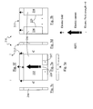
- FIG. 3 there is shown a layout of an unfolded conductive layer 112, including a generally rectangular loop slot 114, ground plane 118, and radiator lamina 116, which is generally similar to the conductive layer 12 of antenna 10 and, accordingly, like numerals are used to indicate like parts (although the values of dimensions L, W, a and b need not necessarily be the same as for antenna 10).
- the ground plane 118 is reduced in size in comparison with the ground plane 18 of antenna 10 such that the ground plane 118 comprises a strip of conductive material which substantially surrounds the slot 114.
- the width W1 of the ground plane 118 may be similar to, or comparable with, the width s of the slot 114. It is preferred that the antenna 110, and more particularly the lamina 116, is fed from a side or edge (as illustrated in Figure 3) and hence the feed point 120 is located at the side or edge 117 of the lamina 116 defined by the slot portions 126. Preferably, the feed point 120 is located substantially at the mid-point of the edge 117.
- the lamina 116 is typically generally rectangular in shape, the feed point 120 typically being located on one of the longer edges (when the aspect ratio is other than 1:1).
- the feed line 121 may comprise a coplanar waveguide or may comprise any other suitable feed mechanism, for example a microstrip line (not illustrated).
- portions of the ground plane are removed to provide a gap between the ground plane 118 for the slot-loop and the ground plane 118' for the feed line 121.
- the slot-loop ground plane 118 and the feed line ground plane 118' are joined by bridge portions 119 and the gap runs substantially parallel with the second slot portions 126. It will be understood, however, that it is equally possible to fold an antenna of the type illustrated in Figure 1 without removing any portions from the ground plane.
- the conductive layer 112 is suitable for use as a planar slot-loop antenna on its own or when provided on a substrate, for example a layer of dielectric material (not shown) or other suitable material.
- a first notional fold line F1 is shown between the feed portion 120 and the third slot portion 128, the fold line F1 running substantially perpendicular to, and intersecting, the first and second slot portions 124, 126 and, in the present embodiment, running substantially parallel with the longitudinal axis of the feed line 121.
- a second notional fold line F2 is similarly provided between the feed portion 120 and the fourth slot portion 130.
- the fold lines F1 and F2 are positioned to notionally divide the conductive layer 112 into three regions: a main or central region 132 of width Wb (which includes the feed point 120) defined between the fold lines F1 and F2, the slot portions of which, during fundamental resonance mode, are associated with an appreciable electric field or magnetic current; a first end region 134 defined beyond the fold line F1 with respect to the central region 132, the slot portions of which, during fundamental resonance mode, are associated with substantially zero electric field or magnetic current; and a second end region 136 defined beyond the fold line F2 with respect to the central region 132, the slot portions of which, during fundamental resonance mode, are associated with substantially zero electric field or magnetic current.
- the end regions 134, 136 may be folded to lie in a plane, or respective planes, that are non-coplanar with the plane in which the central region 132 lies (i.e. the primary plane of the planar antenna) without adversely affecting bandwidth or radiation efficiency.
- the conductive layer 112 is folded in on itself so that the end regions 134, 136 lie in a common plane that is substantially parallel with the plane in which the central region 132 lies.
- two further notional fold lines F1', F2' are defined, each being substantially parallel with the respective fold lines F1, F2 and located in a respective end region 134, 136.
- the respective end region 134, 136 (or at least the portion of the respective end regions 134, 136 beyond the respective fold lines F1', F2') are folded through approximately 180° with respect to the central region 132.
- the spacing Ws between fold line pairs F1, F1' and F2, F2' are equal so that the folded end regions 134, 136 lie in a common plane.
- the electromagnetic fields generated in the resonant modes are said to be associated with respective portions of the slot 14, 114. It may also be said that the electromagnetic fields are associated with adjacent portions (typically the edges) of the lamina 16, 116 itself, since the edges of the lamina 16, 116 partially define the slot 14, 114.
- a planar rectangular slot-loop antenna 110 comprising the conductive layer 112 provided on a generally rectangular substrate layer 115 (e.g. of dielectric material) which has a width substantially equal to Wb , a length substantially equal to a , and a thickness of approximately Ws.
- the antenna 110 has a generally rectangular obverse face (Figure 2a) and a generally rectangular reverse face (Figure 2b) joined by four generally rectangular side faces ( Figures 2c to 2f).
- the obverse face and reverse face are generally parallel and oppositely disposed with respect to one another, the side faces being generally perpendicular to the obverse and reverse faces.
- the conductive layer 112 is provided on the substrate layer 115 such that the central region 132, including the feed portion 120, is located on the obverse face and that the end regions 134, 136 are located partly on opposing side faces ( Figures 2c and 2d) but mainly on the reverse face.
- the slot 14 is folded around the substrate layer 115 so that the portions of the slot 114 which, during fundamental resonance mode, are associated with a significant electric or magnetic field are located on the obverse face, while the portions of the slot 114 which, during fundamental resonance mode, are associated with negligible or substantially zero electric or magnetic field are located mainly on the reverse face.
- the close proximity of the end regions 134, 136 and their respective slot portions on the reverse face of the antenna 110 does not cause mutual interference because the slot portions are associated with little or no magnetic current/electric field.
- the maximum magnetic current points along the slot 14 (and correspondingly the locations of the maximum electric field across the slot 14) occur substantially at the mid-point of the slot portions 124, 126 on the obverse face of the antenna 110.
- any significant magnetic current in, or electric field across, the slot 14 is associated with regions of the slot portions 124, 126 that are located on the obverse face of the antenna 110. Accordingly, the behaviour of the near-field electromagnetic fields in the antenna 110 are not adversely affected when compared to a corresponding unfolded antenna.
- the overall width Wb of the antenna 110 is significantly less than the width W of a corresponding unfolded antenna (and so the area of antenna 110 is correspondingly reduced) without adversely affecting the performance of the antenna 110 in terms of bandwidth or radiation efficiency in comparison with the corresponding unfolded antenna.
- FIG. 5a to 5f illustrate a folded planar lamina antenna, in the preferred form of a planar monopole antenna.
- FIGs 4a to 4f there is shown an unfolded planar antenna 210, or lamina antenna, comprising a layer 212 of conductive material which defines a radiator lamina 216.
- the radiator lamina 216 serves as the resonant structure of the antenna 210 during use.
- a feed line 221 is provided for supplying electromagnetic signals to, and/or receiving electromagnetic signals from, the lamina 216.
- Figure 4a shows the obverse face of the antenna 210
- Figure 4b shows the reverse face
- Figures 4c to 4f each show a respective side face.
- the lamina 216 is carried wholly by the obverse face
- the reverse face of the antenna 210 comprises substrate carrying no conductive material
- the only side face to carry conductive material is the side face associated with the feed line 220.
- the antenna 210 is generally similar to the antennas 10, 110 with the peripheral ground plane 18, 118 (and therefore the slot 14, 114) removed.
- the antenna 210 behaves as a quarter-wavelength planar monopole antenna.
- the main resonant electric current path originates at, or adjacent, the feed point 220 at the centre of the edge 217 of the lamina 216 (shown as point A), and extends to a region or point between the centre of the opposite edge 223 of the lamina 216 (point B) and the centre of the other edges 225 (i.e.
- the edges running between edges 217, 223) of the lamina 216 (points C).
- the actual electric current path depends on the excitation frequency, and the lowest well-matched frequency is determined by the length L between Point A and Point B.
- the bandwidth of the planar monopole is relatively large, the practical upper limit being approximately set by the half-width W/2 (where W is the length of edges 217, 223 and, in the present example, W/2 is the distance from the feed point 220 to the corner at the intersection of edges 217, 225).
- W is the length of edges 217, 223 and, in the present example, W/2 is the distance from the feed point 220 to the corner at the intersection of edges 217, 225).
- the electric field is near, or substantially, zero at or adjacent the feed point 220 and increases to a maximum at the respective Points B and C, depending on excitation frequency.
- the antenna 210 may be folded in a manner similar to that described in relation to Figures 1 to 3 in order to reduce the size of the antenna 210 (in a direction parallel with edges 217, 223). It is found that folding the antenna 210 in this way does not have a significant effect on the bandwidth in comparison with a corresponding unfolded planar monopole antenna.
- Figures 5a to 5f show the antenna 210 folded to produce a folded lamina antenna 210.
- Figure 5a shows the obverse face of the antenna 210
- Figure 5b shows the reverse face
- Figures 5c to 5f each show a respective side face.
- a central region 232 (including the feed point 220) of the lamina 216 is provided on the obverse face of the antenna 210 and that first and second end regions 234, 236 of the lamina 216 are located on the reverse face of the antenna 210, where the central region 232 is located between the end regions 234, 236 when the lamina 216 is unfolded.
- the end regions 234, 236 include the edges 225. Because the lamina 216 is folded or wrapped around the substrate layer 218, the sides of the antenna 210 ( Figures 5c and 5d) each carry a portion of the lamina 216.
- the antennas 110, 210 are generally planar in form although they may more accurately be described as folded planar antennas.
- the invention is not limited to use with antennas in which the conductive layer is carried by a substrate.
- a conductive layer 12, 112 of the type shown in Figures 1 and 3 may be used as antenna and may be folded in the manner described herein without the presence of a supporting substrate layer.
- one or more end regions 334, 336 (including some of slot portions 324, 326 and slot portions 328, 330) of the conductive layer and the respective portions of the substrate layer 315 on which they lie are folded to lie in a plane that is substantially parallel with the primary plane in which the central region of the conductive layer lies.
- the substrate 315 may be folded so as to define a gap, or cavity, between the folded substrate portion(s) and the unfolded substrate portion.
- the antenna 310 is shown with its reverse face facing upwardly.
- the obverse face (not visible in Figure 6) may be generally similar to the obverse face of the antenna 110 shown in Figure 2a.
- the invention is not limited to use with rectangular loop slots.
- the loop slot may take a variety of alternative shapes comprising straight and/or curved sides.
- the invention is not limited to use with planar antenna that are generally rectangular in shape.
Priority Applications (5)
| Application Number | Priority Date | Filing Date | Title |
|---|---|---|---|
| EP04010663A EP1594187B1 (de) | 2004-05-05 | 2004-05-05 | Gefaltete flächige Antenne |
| DE602004020867T DE602004020867D1 (de) | 2004-05-05 | 2004-05-05 | Gefaltete flächige Antenne |
| AT04010663T ATE430388T1 (de) | 2004-05-05 | 2004-05-05 | Gefaltete flächige antenne |
| US11/117,494 US7042402B2 (en) | 2004-05-05 | 2005-04-29 | Planar antenna |
| JP2005133937A JP4373960B2 (ja) | 2004-05-05 | 2005-05-02 | 平面アンテナ |
Applications Claiming Priority (1)
| Application Number | Priority Date | Filing Date | Title |
|---|---|---|---|
| EP04010663A EP1594187B1 (de) | 2004-05-05 | 2004-05-05 | Gefaltete flächige Antenne |
Publications (2)
| Publication Number | Publication Date |
|---|---|
| EP1594187A1 true EP1594187A1 (de) | 2005-11-09 |
| EP1594187B1 EP1594187B1 (de) | 2009-04-29 |
Family
ID=34924861
Family Applications (1)
| Application Number | Title | Priority Date | Filing Date |
|---|---|---|---|
| EP04010663A Expired - Lifetime EP1594187B1 (de) | 2004-05-05 | 2004-05-05 | Gefaltete flächige Antenne |
Country Status (5)
| Country | Link |
|---|---|
| US (1) | US7042402B2 (de) |
| EP (1) | EP1594187B1 (de) |
| JP (1) | JP4373960B2 (de) |
| AT (1) | ATE430388T1 (de) |
| DE (1) | DE602004020867D1 (de) |
Cited By (6)
| Publication number | Priority date | Publication date | Assignee | Title |
|---|---|---|---|---|
| GB2422723B (en) * | 2005-02-01 | 2007-04-18 | Antenova Ltd | Balanced-Unbalanced Antennas |
| US7548211B2 (en) | 2006-03-30 | 2009-06-16 | Phonak Ag | Wireless audio signal receiver device for a hearing instrument |
| CN1925223B (zh) * | 2006-09-21 | 2010-05-12 | 电子科技大学 | 一种具有双折叠槽结构的方向图可重构天线及其阵列 |
| EP2257080A1 (de) | 2006-03-30 | 2010-12-01 | Phonak Ag | Drahtloses Audiosignalsempfängsgerät für ein Hörgerät |
| US9743198B2 (en) | 2014-01-15 | 2017-08-22 | Starkey Laboratories, Inc. | Systems and methods for hearing assistance device antenna |
| WO2018006260A1 (zh) * | 2016-07-05 | 2018-01-11 | 华为技术有限公司 | 一种天线设备和用于天线设备的波束方向调整方法 |
Families Citing this family (24)
| Publication number | Priority date | Publication date | Assignee | Title |
|---|---|---|---|---|
| US7592968B2 (en) * | 2006-03-23 | 2009-09-22 | Tdk Corporation | Embedded antenna |
| US7646341B1 (en) * | 2006-06-19 | 2010-01-12 | National Taiwan University | Ultra-wideband (UWB) antenna |
| US7646346B2 (en) * | 2006-11-10 | 2010-01-12 | Sony Ericsson Mobile Communications Ab | Antenna for a pen-shaped mobile phone |
| US9286481B2 (en) * | 2007-01-18 | 2016-03-15 | Honeywell International Inc. | System and method for secure and distributed physical access control using smart cards |
| US7646347B2 (en) | 2007-01-26 | 2010-01-12 | Sony Ericsson Mobile Communications Ab | Antenna for a pen-shaped mobile phone |
| US7528676B2 (en) * | 2007-04-16 | 2009-05-05 | Tdk Corporation | Balun circuit suitable for integration with chip antenna |
| TW201015788A (en) * | 2008-10-08 | 2010-04-16 | Sunplus Mmobile Inc | Antenna |
| US9412061B2 (en) | 2010-08-13 | 2016-08-09 | Avery Dennison Corporation | Sensing radio frequency identification device with reactive strap attachment |
| US9092709B2 (en) * | 2010-08-25 | 2015-07-28 | Avery Dennison Corporation | RFID tag including environmentally sensitive materials |
| TWI414222B (zh) * | 2010-10-15 | 2013-11-01 | Altek Corp | 於手機中彎折軟性電路板連接之方法及其軟性電路板 |
| US9299021B2 (en) * | 2010-11-11 | 2016-03-29 | Avery Dennison Corporation | RFID devices and methods for manufacturing |
| KR101379123B1 (ko) | 2010-12-17 | 2014-03-31 | 주식회사 케이티 | 광대역 단일 공진 안테나 |
| KR101446248B1 (ko) | 2010-12-29 | 2014-10-01 | 주식회사 케이티 | 선형 배열을 이용한 외장형 안테나 |
| US20120214424A1 (en) * | 2011-02-23 | 2012-08-23 | Mediatek Inc. | Single Input/Multiple Output (SIMO) or Multiple Input/Single Output (MISO) or Multiple Input/Multiple Output (MIMO) Antenna Module |
| WO2012125186A1 (en) * | 2011-03-15 | 2012-09-20 | Intel Corporation | Conformal phased array antenna with integrated transceiver |
| JP5687536B2 (ja) * | 2011-03-23 | 2015-03-18 | 日精株式会社 | 基板型アンテナ |
| US9112262B2 (en) | 2011-06-02 | 2015-08-18 | Brigham Young University | Planar array feed for satellite communications |
| US9112270B2 (en) | 2011-06-02 | 2015-08-18 | Brigham Young Univeristy | Planar array feed for satellite communications |
| US8870069B2 (en) | 2012-08-22 | 2014-10-28 | Symbol Technologies, Inc. | Co-located antenna arrangement |
| US9099789B1 (en) * | 2012-09-05 | 2015-08-04 | Amazon Technologies, Inc. | Dual-band inverted slot antenna |
| CN104577338B (zh) * | 2013-10-09 | 2019-06-18 | 深圳富泰宏精密工业有限公司 | 天线组件及具有该天线组件的无线通信装置 |
| JP6361431B2 (ja) * | 2014-09-30 | 2018-07-25 | 富士通株式会社 | 周波数特性調整用治具、アンテナ検査装置及びアンテナ検査方法及びならびにループアンテナ |
| KR20160045312A (ko) | 2014-10-17 | 2016-04-27 | 삼성전자주식회사 | 안테나 장치 및 그를 포함하는 전자 장치 |
| US10236559B2 (en) * | 2017-04-14 | 2019-03-19 | Futurewei Technologies, Inc. | Three-slotted antenna apparatus and method |
Citations (5)
| Publication number | Priority date | Publication date | Assignee | Title |
|---|---|---|---|---|
| US3623162A (en) * | 1970-07-24 | 1971-11-23 | Sanders Associates Inc | Folded slot antenna |
| JP2000059125A (ja) * | 1998-08-11 | 2000-02-25 | Tdk Corp | チップアンテナ |
| US6124831A (en) * | 1999-07-22 | 2000-09-26 | Ericsson Inc. | Folded dual frequency band antennas for wireless communicators |
| EP1176664A2 (de) * | 2000-07-24 | 2002-01-30 | The Furukawa Electric Co., Ltd. | Chip-Antenne und Verfahren zur Herstellung einer derartigen Antenne |
| US6407715B1 (en) * | 2001-05-04 | 2002-06-18 | Acer Communications And Multimedia Inc. | Dual frequency band antenna with folded structure and related method |
Family Cites Families (22)
| Publication number | Priority date | Publication date | Assignee | Title |
|---|---|---|---|---|
| DE861114C (de) | 1951-10-11 | 1952-12-29 | Max Grundig | Einbauantennen fuer Fernseh- und UKW-Empfaenger |
| KR920002439B1 (ko) * | 1988-08-31 | 1992-03-24 | 삼성전자 주식회사 | 휴대용 무선전화기의 슬로트 안테나 장치 |
| GB2276274B (en) | 1993-03-17 | 1997-10-22 | Seiko Epson Corp | Slot antenna device |
| US5757326A (en) * | 1993-03-29 | 1998-05-26 | Seiko Epson Corporation | Slot antenna device and wireless apparatus employing the antenna device |
| DE59507497D1 (de) | 1994-02-24 | 2000-02-03 | Ascom Ag Bern | Tragbares Funkgerät |
| US5781158A (en) * | 1995-04-25 | 1998-07-14 | Young Hoek Ko | Electric/magnetic microstrip antenna |
| DE59708915D1 (de) * | 1996-03-13 | 2003-01-23 | Ascom Systec Ag Maegenwil | Flache dreidimensionale Antenne |
| FR2752646B1 (fr) * | 1996-08-21 | 1998-11-13 | France Telecom | Antenne imprimee plane a elements superposes court-circuites |
| DE69726523T2 (de) | 1996-09-12 | 2004-09-30 | Mitsubishi Materials Corp. | Antenne |
| US5754143A (en) * | 1996-10-29 | 1998-05-19 | Southwest Research Institute | Switch-tuned meandered-slot antenna |
| US6198437B1 (en) * | 1998-07-09 | 2001-03-06 | The United States Of America As Represented By The Secretary Of The Air Force | Broadband patch/slot antenna |
| JP3344333B2 (ja) | 1998-10-22 | 2002-11-11 | 株式会社村田製作所 | フィルタ内蔵誘電体アンテナ、デュプレクサ内蔵誘電体アンテナおよび無線装置 |
| US6452554B1 (en) * | 1998-11-06 | 2002-09-17 | Hitachi Metals, Ltd. | Antenna element and radio communication apparatus |
| US6049314A (en) * | 1998-11-17 | 2000-04-11 | Xertex Technologies, Inc. | Wide band antenna having unitary radiator/ground plane |
| SE513525C2 (sv) * | 1998-11-20 | 2000-09-25 | Smarteq Ab | En antennanordning |
| US6343208B1 (en) * | 1998-12-16 | 2002-01-29 | Telefonaktiebolaget Lm Ericsson (Publ) | Printed multi-band patch antenna |
| JP4327982B2 (ja) * | 1999-05-28 | 2009-09-09 | 株式会社日本自動車部品総合研究所 | 携帯型無線機用アンテナ |
| US6414642B2 (en) * | 1999-12-17 | 2002-07-02 | Tyco Electronics Logistics Ag | Orthogonal slot antenna assembly |
| JP2001257519A (ja) * | 2000-03-09 | 2001-09-21 | Alps Electric Co Ltd | アンテナ |
| US6518924B1 (en) * | 2001-08-13 | 2003-02-11 | Ethertronics, Inc. | Integrated multifrequency slot/patch antenna and method |
| US6417809B1 (en) * | 2001-08-15 | 2002-07-09 | Centurion Wireless Technologies, Inc. | Compact dual diversity antenna for RF data and wireless communication devices |
| TW541759B (en) * | 2002-07-24 | 2003-07-11 | Ind Tech Res Inst | Foldable dual-band monopole antenna |
-
2004
- 2004-05-05 DE DE602004020867T patent/DE602004020867D1/de not_active Expired - Lifetime
- 2004-05-05 EP EP04010663A patent/EP1594187B1/de not_active Expired - Lifetime
- 2004-05-05 AT AT04010663T patent/ATE430388T1/de not_active IP Right Cessation
-
2005
- 2005-04-29 US US11/117,494 patent/US7042402B2/en active Active
- 2005-05-02 JP JP2005133937A patent/JP4373960B2/ja not_active Expired - Fee Related
Patent Citations (5)
| Publication number | Priority date | Publication date | Assignee | Title |
|---|---|---|---|---|
| US3623162A (en) * | 1970-07-24 | 1971-11-23 | Sanders Associates Inc | Folded slot antenna |
| JP2000059125A (ja) * | 1998-08-11 | 2000-02-25 | Tdk Corp | チップアンテナ |
| US6124831A (en) * | 1999-07-22 | 2000-09-26 | Ericsson Inc. | Folded dual frequency band antennas for wireless communicators |
| EP1176664A2 (de) * | 2000-07-24 | 2002-01-30 | The Furukawa Electric Co., Ltd. | Chip-Antenne und Verfahren zur Herstellung einer derartigen Antenne |
| US6407715B1 (en) * | 2001-05-04 | 2002-06-18 | Acer Communications And Multimedia Inc. | Dual frequency band antenna with folded structure and related method |
Non-Patent Citations (1)
| Title |
|---|
| PATENT ABSTRACTS OF JAPAN vol. 2000, no. 05 14 September 2000 (2000-09-14) * |
Cited By (13)
| Publication number | Priority date | Publication date | Assignee | Title |
|---|---|---|---|---|
| GB2422723B (en) * | 2005-02-01 | 2007-04-18 | Antenova Ltd | Balanced-Unbalanced Antennas |
| EP2257079A1 (de) | 2006-03-30 | 2010-12-01 | Phonak Ag | Drahtloses Audiosignalsempfängsgerät für ein Hörgerät |
| US7777681B2 (en) | 2006-03-30 | 2010-08-17 | Phonak Ag | Wireless audio signal receiver device for a hearing instrument |
| US7791551B2 (en) | 2006-03-30 | 2010-09-07 | Phonak Ag | Wireless audio signal receiver device for a hearing instrument |
| EP2257080A1 (de) | 2006-03-30 | 2010-12-01 | Phonak Ag | Drahtloses Audiosignalsempfängsgerät für ein Hörgerät |
| US7548211B2 (en) | 2006-03-30 | 2009-06-16 | Phonak Ag | Wireless audio signal receiver device for a hearing instrument |
| CN1925223B (zh) * | 2006-09-21 | 2010-05-12 | 电子科技大学 | 一种具有双折叠槽结构的方向图可重构天线及其阵列 |
| US9743198B2 (en) | 2014-01-15 | 2017-08-22 | Starkey Laboratories, Inc. | Systems and methods for hearing assistance device antenna |
| US10405109B2 (en) | 2014-01-15 | 2019-09-03 | Starkey Laboratories, Inc. | Systems and methods for hearing assistance device antenna |
| WO2018006260A1 (zh) * | 2016-07-05 | 2018-01-11 | 华为技术有限公司 | 一种天线设备和用于天线设备的波束方向调整方法 |
| CN107851892A (zh) * | 2016-07-05 | 2018-03-27 | 华为技术有限公司 | 一种天线设备和用于天线设备的波束方向调整方法 |
| CN107851892B (zh) * | 2016-07-05 | 2019-12-17 | 华为技术有限公司 | 一种天线设备和用于天线设备的波束方向调整方法 |
| US10862215B2 (en) | 2016-07-05 | 2020-12-08 | Huawei Technologies Co., Ltd. | Antenna device and beam direction adjustment method applied to antenna device |
Also Published As
| Publication number | Publication date |
|---|---|
| US20050248488A1 (en) | 2005-11-10 |
| EP1594187B1 (de) | 2009-04-29 |
| JP2005323368A (ja) | 2005-11-17 |
| DE602004020867D1 (de) | 2009-06-10 |
| ATE430388T1 (de) | 2009-05-15 |
| JP4373960B2 (ja) | 2009-11-25 |
| US7042402B2 (en) | 2006-05-09 |
Similar Documents
| Publication | Publication Date | Title |
|---|---|---|
| US7042402B2 (en) | Planar antenna | |
| US7592968B2 (en) | Embedded antenna | |
| EP2230717B1 (de) | Breitbandige, hoch isolierte Antennenanordnung mit zwei Anschlüssen für tragbare, MIMO-fähige Geräte | |
| KR101025680B1 (ko) | 안테나 장치 및 휴대 무선 통신 단말기 | |
| US7274334B2 (en) | Stacked multi-resonator antenna | |
| JP4423809B2 (ja) | 複共振アンテナ | |
| JP2001522558A (ja) | 無線通信装置用アンテナ | |
| KR20110129452A (ko) | 균형 메타 재료 안테나 장치 | |
| JP2002057523A (ja) | 導電層を有するアンテナおよびアンテナを含む2帯域送信器 | |
| JP2002517925A (ja) | アンテナ | |
| JP3255403B2 (ja) | パッチアンテナおよびそれを用いた電子機器 | |
| JP4268585B2 (ja) | アンテナ装置 | |
| KR20010101891A (ko) | 마이크로 스트립 안테나 | |
| JP3234393B2 (ja) | アンテナ装置 | |
| JP2002100915A (ja) | 誘電体アンテナ | |
| JP2013530623A (ja) | 平面導電素子を有するアンテナ | |
| JP3839393B2 (ja) | 2周波共用アンテナ装置 | |
| US6437744B1 (en) | Circularly polarized wave antenna device | |
| JP2003168916A (ja) | アンテナ装置 | |
| JP3286894B2 (ja) | 表面実装型アンテナ | |
| JP2003037423A (ja) | 表面実装型アンテナおよびそれを搭載した通信機器 | |
| CN109088168B (zh) | 一种移动终端天线和移动终端 | |
| JP3838971B2 (ja) | 無線装置 | |
| KR100581712B1 (ko) | 이동통신단말기용 링형 안테나 구조 | |
| JPH05343915A (ja) | マイクロストリップアンテナ |
Legal Events
| Date | Code | Title | Description |
|---|---|---|---|
| PUAI | Public reference made under article 153(3) epc to a published international application that has entered the european phase |
Free format text: ORIGINAL CODE: 0009012 |
|
| AK | Designated contracting states |
Kind code of ref document: A1 Designated state(s): AT BE BG CH CY CZ DE DK EE ES FI FR GB GR HU IE IT LI LU MC NL PL PT RO SE SI SK TR |
|
| AX | Request for extension of the european patent |
Extension state: AL HR LT LV MK |
|
| 17P | Request for examination filed |
Effective date: 20060322 |
|
| AKX | Designation fees paid |
Designated state(s): AT BE BG CH CY CZ DE DK EE ES FI FR GB GR HU IE IT LI LU MC NL PL PT RO SE SI SK TR |
|
| GRAP | Despatch of communication of intention to grant a patent |
Free format text: ORIGINAL CODE: EPIDOSNIGR1 |
|
| RIC1 | Information provided on ipc code assigned before grant |
Ipc: H01Q 9/42 20060101ALI20081110BHEP Ipc: H01Q 1/24 20060101ALI20081110BHEP Ipc: H01Q 13/10 20060101AFI20081110BHEP |
|
| GRAS | Grant fee paid |
Free format text: ORIGINAL CODE: EPIDOSNIGR3 |
|
| GRAA | (expected) grant |
Free format text: ORIGINAL CODE: 0009210 |
|
| AK | Designated contracting states |
Kind code of ref document: B1 Designated state(s): AT BE BG CH CY CZ DE DK EE ES FI FR GB GR HU IE IT LI LU MC NL PL PT RO SE SI SK TR |
|
| REG | Reference to a national code |
Ref country code: GB Ref legal event code: FG4D |
|
| REG | Reference to a national code |
Ref country code: CH Ref legal event code: EP |
|
| REF | Corresponds to: |
Ref document number: 602004020867 Country of ref document: DE Date of ref document: 20090610 Kind code of ref document: P |
|
| REG | Reference to a national code |
Ref country code: IE Ref legal event code: FG4D |
|
| NLV1 | Nl: lapsed or annulled due to failure to fulfill the requirements of art. 29p and 29m of the patents act | ||
| PG25 | Lapsed in a contracting state [announced via postgrant information from national office to epo] |
Ref country code: AT Free format text: LAPSE BECAUSE OF FAILURE TO SUBMIT A TRANSLATION OF THE DESCRIPTION OR TO PAY THE FEE WITHIN THE PRESCRIBED TIME-LIMIT Effective date: 20090429 Ref country code: FI Free format text: LAPSE BECAUSE OF FAILURE TO SUBMIT A TRANSLATION OF THE DESCRIPTION OR TO PAY THE FEE WITHIN THE PRESCRIBED TIME-LIMIT Effective date: 20090429 Ref country code: ES Free format text: LAPSE BECAUSE OF FAILURE TO SUBMIT A TRANSLATION OF THE DESCRIPTION OR TO PAY THE FEE WITHIN THE PRESCRIBED TIME-LIMIT Effective date: 20090809 Ref country code: PT Free format text: LAPSE BECAUSE OF FAILURE TO SUBMIT A TRANSLATION OF THE DESCRIPTION OR TO PAY THE FEE WITHIN THE PRESCRIBED TIME-LIMIT Effective date: 20090829 |
|
| PG25 | Lapsed in a contracting state [announced via postgrant information from national office to epo] |
Ref country code: SE Free format text: LAPSE BECAUSE OF FAILURE TO SUBMIT A TRANSLATION OF THE DESCRIPTION OR TO PAY THE FEE WITHIN THE PRESCRIBED TIME-LIMIT Effective date: 20090729 Ref country code: NL Free format text: LAPSE BECAUSE OF FAILURE TO SUBMIT A TRANSLATION OF THE DESCRIPTION OR TO PAY THE FEE WITHIN THE PRESCRIBED TIME-LIMIT Effective date: 20090429 Ref country code: PL Free format text: LAPSE BECAUSE OF FAILURE TO SUBMIT A TRANSLATION OF THE DESCRIPTION OR TO PAY THE FEE WITHIN THE PRESCRIBED TIME-LIMIT Effective date: 20090429 Ref country code: SI Free format text: LAPSE BECAUSE OF FAILURE TO SUBMIT A TRANSLATION OF THE DESCRIPTION OR TO PAY THE FEE WITHIN THE PRESCRIBED TIME-LIMIT Effective date: 20090429 |
|
| PG25 | Lapsed in a contracting state [announced via postgrant information from national office to epo] |
Ref country code: MC Free format text: LAPSE BECAUSE OF NON-PAYMENT OF DUE FEES Effective date: 20090531 |
|
| REG | Reference to a national code |
Ref country code: CH Ref legal event code: PL |
|
| PG25 | Lapsed in a contracting state [announced via postgrant information from national office to epo] |
Ref country code: RO Free format text: LAPSE BECAUSE OF FAILURE TO SUBMIT A TRANSLATION OF THE DESCRIPTION OR TO PAY THE FEE WITHIN THE PRESCRIBED TIME-LIMIT Effective date: 20090429 Ref country code: LI Free format text: LAPSE BECAUSE OF NON-PAYMENT OF DUE FEES Effective date: 20090531 Ref country code: EE Free format text: LAPSE BECAUSE OF FAILURE TO SUBMIT A TRANSLATION OF THE DESCRIPTION OR TO PAY THE FEE WITHIN THE PRESCRIBED TIME-LIMIT Effective date: 20090429 Ref country code: CH Free format text: LAPSE BECAUSE OF NON-PAYMENT OF DUE FEES Effective date: 20090531 Ref country code: CZ Free format text: LAPSE BECAUSE OF FAILURE TO SUBMIT A TRANSLATION OF THE DESCRIPTION OR TO PAY THE FEE WITHIN THE PRESCRIBED TIME-LIMIT Effective date: 20090429 Ref country code: DK Free format text: LAPSE BECAUSE OF FAILURE TO SUBMIT A TRANSLATION OF THE DESCRIPTION OR TO PAY THE FEE WITHIN THE PRESCRIBED TIME-LIMIT Effective date: 20090429 |
|
| PG25 | Lapsed in a contracting state [announced via postgrant information from national office to epo] |
Ref country code: SK Free format text: LAPSE BECAUSE OF FAILURE TO SUBMIT A TRANSLATION OF THE DESCRIPTION OR TO PAY THE FEE WITHIN THE PRESCRIBED TIME-LIMIT Effective date: 20090429 Ref country code: BE Free format text: LAPSE BECAUSE OF FAILURE TO SUBMIT A TRANSLATION OF THE DESCRIPTION OR TO PAY THE FEE WITHIN THE PRESCRIBED TIME-LIMIT Effective date: 20090429 |
|
| PLBE | No opposition filed within time limit |
Free format text: ORIGINAL CODE: 0009261 |
|
| STAA | Information on the status of an ep patent application or granted ep patent |
Free format text: STATUS: NO OPPOSITION FILED WITHIN TIME LIMIT |
|
| REG | Reference to a national code |
Ref country code: IE Ref legal event code: MM4A |
|
| PG25 | Lapsed in a contracting state [announced via postgrant information from national office to epo] |
Ref country code: BG Free format text: LAPSE BECAUSE OF FAILURE TO SUBMIT A TRANSLATION OF THE DESCRIPTION OR TO PAY THE FEE WITHIN THE PRESCRIBED TIME-LIMIT Effective date: 20090729 |
|
| 26N | No opposition filed |
Effective date: 20100201 |
|
| PG25 | Lapsed in a contracting state [announced via postgrant information from national office to epo] |
Ref country code: IE Free format text: LAPSE BECAUSE OF NON-PAYMENT OF DUE FEES Effective date: 20090505 |
|
| PG25 | Lapsed in a contracting state [announced via postgrant information from national office to epo] |
Ref country code: GR Free format text: LAPSE BECAUSE OF FAILURE TO SUBMIT A TRANSLATION OF THE DESCRIPTION OR TO PAY THE FEE WITHIN THE PRESCRIBED TIME-LIMIT Effective date: 20090730 |
|
| PG25 | Lapsed in a contracting state [announced via postgrant information from national office to epo] |
Ref country code: IT Free format text: LAPSE BECAUSE OF FAILURE TO SUBMIT A TRANSLATION OF THE DESCRIPTION OR TO PAY THE FEE WITHIN THE PRESCRIBED TIME-LIMIT Effective date: 20090429 |
|
| PG25 | Lapsed in a contracting state [announced via postgrant information from national office to epo] |
Ref country code: LU Free format text: LAPSE BECAUSE OF NON-PAYMENT OF DUE FEES Effective date: 20090505 |
|
| PG25 | Lapsed in a contracting state [announced via postgrant information from national office to epo] |
Ref country code: HU Free format text: LAPSE BECAUSE OF FAILURE TO SUBMIT A TRANSLATION OF THE DESCRIPTION OR TO PAY THE FEE WITHIN THE PRESCRIBED TIME-LIMIT Effective date: 20091030 |
|
| PG25 | Lapsed in a contracting state [announced via postgrant information from national office to epo] |
Ref country code: TR Free format text: LAPSE BECAUSE OF FAILURE TO SUBMIT A TRANSLATION OF THE DESCRIPTION OR TO PAY THE FEE WITHIN THE PRESCRIBED TIME-LIMIT Effective date: 20090429 |
|
| PG25 | Lapsed in a contracting state [announced via postgrant information from national office to epo] |
Ref country code: CY Free format text: LAPSE BECAUSE OF FAILURE TO SUBMIT A TRANSLATION OF THE DESCRIPTION OR TO PAY THE FEE WITHIN THE PRESCRIBED TIME-LIMIT Effective date: 20090429 |
|
| REG | Reference to a national code |
Ref country code: FR Ref legal event code: PLFP Year of fee payment: 12 |
|
| REG | Reference to a national code |
Ref country code: FR Ref legal event code: PLFP Year of fee payment: 13 |
|
| REG | Reference to a national code |
Ref country code: FR Ref legal event code: PLFP Year of fee payment: 14 |
|
| PGFP | Annual fee paid to national office [announced via postgrant information from national office to epo] |
Ref country code: DE Payment date: 20170502 Year of fee payment: 14 |
|
| REG | Reference to a national code |
Ref country code: FR Ref legal event code: PLFP Year of fee payment: 15 |
|
| PGFP | Annual fee paid to national office [announced via postgrant information from national office to epo] |
Ref country code: GB Payment date: 20180329 Year of fee payment: 15 |
|
| PGFP | Annual fee paid to national office [announced via postgrant information from national office to epo] |
Ref country code: FR Payment date: 20180411 Year of fee payment: 15 |
|
| REG | Reference to a national code |
Ref country code: DE Ref legal event code: R119 Ref document number: 602004020867 Country of ref document: DE |
|
| PG25 | Lapsed in a contracting state [announced via postgrant information from national office to epo] |
Ref country code: DE Free format text: LAPSE BECAUSE OF NON-PAYMENT OF DUE FEES Effective date: 20181201 |
|
| GBPC | Gb: european patent ceased through non-payment of renewal fee |
Effective date: 20190505 |
|
| PG25 | Lapsed in a contracting state [announced via postgrant information from national office to epo] |
Ref country code: GB Free format text: LAPSE BECAUSE OF NON-PAYMENT OF DUE FEES Effective date: 20190505 |
|
| PG25 | Lapsed in a contracting state [announced via postgrant information from national office to epo] |
Ref country code: FR Free format text: LAPSE BECAUSE OF NON-PAYMENT OF DUE FEES Effective date: 20190531 |