EP1593996A2 - Beleuchtungs-Anordnung für die Fluoreszenz-Mikroskopie - Google Patents
Beleuchtungs-Anordnung für die Fluoreszenz-Mikroskopie Download PDFInfo
- Publication number
- EP1593996A2 EP1593996A2 EP05009607A EP05009607A EP1593996A2 EP 1593996 A2 EP1593996 A2 EP 1593996A2 EP 05009607 A EP05009607 A EP 05009607A EP 05009607 A EP05009607 A EP 05009607A EP 1593996 A2 EP1593996 A2 EP 1593996A2
- Authority
- EP
- European Patent Office
- Prior art keywords
- illumination
- led
- fluorescence
- dimmer
- signal
- Prior art date
- Legal status (The legal status is an assumption and is not a legal conclusion. Google has not performed a legal analysis and makes no representation as to the accuracy of the status listed.)
- Withdrawn
Links
- 238000005286 illumination Methods 0.000 title claims abstract description 91
- 230000003287 optical effect Effects 0.000 claims abstract description 24
- 230000004044 response Effects 0.000 claims description 14
- 238000003384 imaging method Methods 0.000 claims description 3
- 230000005284 excitation Effects 0.000 description 52
- 238000010586 diagram Methods 0.000 description 15
- 230000004907 flux Effects 0.000 description 15
- 238000000799 fluorescence microscopy Methods 0.000 description 9
- 238000012546 transfer Methods 0.000 description 9
- QSHDDOUJBYECFT-UHFFFAOYSA-N mercury Chemical compound [Hg] QSHDDOUJBYECFT-UHFFFAOYSA-N 0.000 description 7
- 229910052753 mercury Inorganic materials 0.000 description 7
- 229910052724 xenon Inorganic materials 0.000 description 7
- FHNFHKCVQCLJFQ-UHFFFAOYSA-N xenon atom Chemical compound [Xe] FHNFHKCVQCLJFQ-UHFFFAOYSA-N 0.000 description 7
- 238000002073 fluorescence micrograph Methods 0.000 description 6
- 230000000694 effects Effects 0.000 description 5
- 238000004061 bleaching Methods 0.000 description 4
- 230000009467 reduction Effects 0.000 description 4
- 230000004888 barrier function Effects 0.000 description 3
- 239000000975 dye Substances 0.000 description 3
- 230000020169 heat generation Effects 0.000 description 3
- 230000004048 modification Effects 0.000 description 3
- 238000012986 modification Methods 0.000 description 3
- 108090000623 proteins and genes Proteins 0.000 description 3
- 108010043121 Green Fluorescent Proteins Proteins 0.000 description 2
- 102000004144 Green Fluorescent Proteins Human genes 0.000 description 2
- 230000005540 biological transmission Effects 0.000 description 2
- 238000004891 communication Methods 0.000 description 2
- 239000003814 drug Substances 0.000 description 2
- 238000005401 electroluminescence Methods 0.000 description 2
- 239000005090 green fluorescent protein Substances 0.000 description 2
- 238000004020 luminiscence type Methods 0.000 description 2
- 238000000034 method Methods 0.000 description 2
- 102000004169 proteins and genes Human genes 0.000 description 2
- 230000035945 sensitivity Effects 0.000 description 2
- BHPQYMZQTOCNFJ-UHFFFAOYSA-N Calcium cation Chemical compound [Ca+2] BHPQYMZQTOCNFJ-UHFFFAOYSA-N 0.000 description 1
- 229910001424 calcium ion Inorganic materials 0.000 description 1
- 238000001816 cooling Methods 0.000 description 1
- 230000003247 decreasing effect Effects 0.000 description 1
- 230000006866 deterioration Effects 0.000 description 1
- 230000006870 function Effects 0.000 description 1
- YFHXZQPUBCBNIP-UHFFFAOYSA-N fura-2 Chemical compound CC1=CC=C(N(CC(O)=O)CC(O)=O)C(OCCOC=2C(=CC=3OC(=CC=3C=2)C=2OC(=CN=2)C(O)=O)N(CC(O)=O)CC(O)=O)=C1 YFHXZQPUBCBNIP-UHFFFAOYSA-N 0.000 description 1
- 238000012423 maintenance Methods 0.000 description 1
- 238000005259 measurement Methods 0.000 description 1
- 230000007246 mechanism Effects 0.000 description 1
- 238000012545 processing Methods 0.000 description 1
- 230000005855 radiation Effects 0.000 description 1
- 238000011160 research Methods 0.000 description 1
- 230000000007 visual effect Effects 0.000 description 1
Images

Classifications
-
- G—PHYSICS
- G02—OPTICS
- G02B—OPTICAL ELEMENTS, SYSTEMS OR APPARATUS
- G02B21/00—Microscopes
- G02B21/16—Microscopes adapted for ultraviolet illumination ; Fluorescence microscopes
Definitions
- the present invention relates to a microscope fluorescence illumination apparatus for use in a fluorescence microscope for observing fluorescence from a living tissue in a research field such as medicine or biology.
- a light source having a continuous wavelength such as a mercury lamp or a xenon lamp is used as a fluorescence observation illuminating apparatus for use in a fluorescence microscope, and the light generated from such a light source is emitted to a sample as excitation light.
- the light from the mercury lamp or xenon lamp has a plenty of wavelength components, and thus, the light from which a specific wavelength component has been extracted is emitted to a sample as excitation light by using a wavelength selecting filter called an excitation filter.
- a wavelength selecting filter called an excitation filter.
- filters are mounted, and further, a filter device enabling switching of these filters is required, thus requiring a large space required for mounting the filter device.
- the mercury lamp and xenon lamp are large in size and much in heat radiation, its handling is inconvenient.
- a fluorescence microscope using solid-state illumination devices such as one or a plurality of light emitting diodes (LEDs), laser diodes (LDs), and organic electro-luminescences (ELs) is devised as a light source.
- LEDs light emitting diodes
- LDs laser diodes
- ELs organic electro-luminescences
- an LED becomes prevailingly known with high luminescence. From among them, an LED emitting white light has been used as an illumination in a variety of fields. In addition, a single color LED is also higher in luminescence or is diversified in light emitting wavelength, and is widely used for display such as a signal indicator. Further, when an LED is used as an illumination light source of a microscope, a plenty of advantages such as free maintenance, downsizing of an illuminating apparatus, low power consumption, and reduction of heat generation can be expected by downsizing, exterminated service life, low heat generation and the like which are features of the LED.
- Jpn. Pat. Appln. KOKAI Publication No. 2001-154103 discloses an illuminating apparatus achieving space reduction and good operability capable of eliminating a variety of adjustments during replacement of a conventional lamp by using an array of white color LEDs and switching a bright-field observation or a dark-field observation of a microscope by switching lighting portions in the same LED array.
- Jpn. Pat. Appln. KOKAI Publication No. 2002-131648 there is provided a fluorescence microscope achieving space reduction which does not require an excitation filter by using it for an illuminating apparatus for a fluorescence microscope by paying attention to the fact that a single color LED is in a wavelength bandwidth of orders of several tens of nm in width. Further, excitation light illumination using the LED is used as a transmission type or incident-light type dark-field optical system, thus enabling fluorescence observation with high sensitivity having an improved signal-to-noise ratio.
- the high speed shutter or the filter turret uses a mechanical mechanism, thus requiring a switching time of several milliseconds to several tens of milliseconds.
- a high speed camera which enables photography of about 500 images per second, for example, even if synchronization with start or end of exposure of this camera is obtained, unnecessary excitation light is emitted to a sample for several milliseconds to several tens of milliseconds.
- the mercury lamp or the xenon lamp is an electric power discharge tube, and cannot adjust a luminous flux continuously.
- dimming is carried out by reducing the luminous flux in stepwise manner using two or three ND filters.
- stepwise dimming has been sufficient.
- weak fluorescence which cannot be recognized with naked eye is acquired as an image by means of a CCD camera having high sensitivity, and the acquired image is analyzed. In this imaging using weak fluorescence, very fine adjustment and high precision are required for dimming of excitation light.
- An object of the present invention is to provide a microscope fluorescence illumination apparatus which is excellent in sample protection, operability, and power saving by using a solid-state illumination device as an illumination light source of fluorescence observation.
- a microscope fluorescence illumination apparatus is characterized by comprising: a light source having a solid-state illumination device which generates illumination light; an illumination optical system which guides the illumination light from the light source onto a sample; and a controller configured to control turning ON and OFF of the solid-state illumination device and dimming of the illumination light.
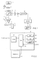
- FIG. 1 shows a schematic configuration of a microscope system using a microscope fluorescence illumination apparatus according to a first embodiment of the present invention.
- a fluorescence sample S is placed as a sample on a stage 1.
- the stage 1 can move vertically in an optical axis direction and the fluorescence sample S can be focused by moving the stage 1 in the vertical direction.
- an objection lens 1 is allocated in proximity with the fluorescence sample S.
- a plurality of objective lenses 3 each having different magnification are held by a nosepiece 2, and the objective lenses 3 are positioned on an optical axis by a rotating operation of the nosepiece 2, whereby the fluorescence sample S can be observed.
- a dichroic mirror 7 is allocated via a condenser 5 or an excitation filter 6 configuring an illumination optical system.
- the condenser 5 converts the light from the LED 4 to parallel light beams, and the excitation filter 6 transmits only the light having a wavelength in a bandwidth required for exciting the fluorescence sample S.
- the dichroic mirror 7 has such a feature of reflecting the excitation light transmitted through the excitation filter 6, and then, transmitting the fluorescence emitted from the fluorescence sample S.
- the fluorescence sample S on the stage 1 is allocated via the objective lens 3, and the excitation light is emitted from above the fluorescence sample S.
- the fluorescence emitted from the fluorescence sample S is produced as light shifted from a wavelength of the excitation light to a long wavelength, and the produced light is transmitted from the objective lens 3 through the dichroic mirror 7.
- a barrier filter 8 and a beam splitter 9 configuring an observation optical system are allocated in an optical path transmitted through the dichroic mirror 7.
- the barrier filter 8 cuts the light other than a bandwidth of fluorescence and acquires an observation image having a good signal-to-noise ratio.
- the beam splitter 9 splits the light which is incident from the barrier filter 8 in two directions.
- An eyepiece 10 is allocated in one optical path and visual observation can be carried out.
- a CCD camera 11 serving as image pickup means which is an external device is allocated in the other optical path, and fluorescence can be picked up as an image.
- a controller 13 is connected,to the LED 4 via an LED driver 12.
- the LED driver 12 controls turning ON/OFF the LED 4 in accordance with an instruction from the controller 13.
- An operation unit 14 serving as a man-machine interface is connected to the controller 13.
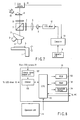
- FIG. 2 is a diagram showing a schematic configuration of the controller 13.
- the controller 13 comprises a CPU 131, a ROM 132, a RAM 133, a nonvolatile memory 134, and a dimmer 135.
- the CPU 131, the ROM 132, the RAM 133, the nonvolatile memory 134, and the dimmer 135 are connected to one another via a CPU bus.
- the ROM 132 stores a program which describes the content of control in the CPU 131.
- the RAM 133 stores data such as control processing.
- An EEPROM, a flash memory or the like is used for the nonvolatile memory 134, and required information is stored in or read from the nonvolatile memory 134 by executing the program.
- the dimmer 135 turns ON/OFF the LED 4 via the LED driver 12 in response to an instruction of turning ON/OFF the LED 4 from the CPU 131.
- the dimmer 135 also outputs a power variable signal to the LED driver 12 in response to a dimming instruction from the CPU 131 and makes dimming control for increasing or decreasing the illumination luminous flux of the LED 4.
- a button 142 and a dimmer dial 143 are allocated on a surface of an operation unit main body 141, and each of these button and dial is connected to the CPU 131.
- the button 142 outputs an operation signal for turning ON/OFF the LED 4 in response to a push operation or a release operation.
- the operation signal can be read out by the CPU 131.
- the dimmer dial 143 outputs a dimming operation signal according to an operation angle (rotation angle).
- the dimming operation signal can be read out by the CPU 131.
- the controller 13 has an external communication unit such as RS-232C, USB, or Ethernet (not shown). From an external device such as a personal computer (PC) (hereinafter, referred to as a host), the CPU 131 transmits and receives a command via an interface (I/F) (not shown), thereby making control equivalent to the operation from the operation unit 14 and making external information exchange.
- PC personal computer
- the LED 4 is turned OFF in an initial state.
- the button 142 on the operation unit 14 is pushed.
- the CPU 131 of the controller 13 detects a push operation of the button 142; reads out an operation angle (rotation angle) of the dimmer dial 143; and outputs to the dimmer 135 an electric power indicator value according to the operation angle.
- the dimmer 135 generates an electric power indicator signal which corresponds to the dimmer indicator value from the CPU 131 and outputs this electric power indicator signal to the LED driver 12.
- the LED driver 12 turns ON the LED 4 at brightness (luminous flux) which corresponds to the dimmer indicator value.
- the CPU 131 detects an amount of dial operation.
- the CPU 131 reads out an operation angle (rotation angle) from the dimmer dial 143, and outputs to the dimmer 135 the dimmer indicator value according to the rotation angle.
- the dimmer 135 outputs the dimmer indicator value from the CPU 131 to the LED driver 12.
- the LED driver 12 outputs an electric power indicator signal which corresponds to the dimmer indicator value from the CPU 131, and turns ON the LED 4 at the brightness which corresponds to the dimmer output value. In this manner, the LED 4 can be turned ON at arbitrary brightness (luminous flux) by adjusting the operation angle (rotation angle) of the dimmer dial 143 on the operation unit 14.
- the CPU 131 detects a release operation of the button 142; determines an instruction for turning OFF power; and outputs a turning OFF signal to the dimmer 135.
- the dimmer 135 outputs a turning OFF signal from the CPU 131 to the LED driver 12.
- the LED driver 12 turns OFF the LED 4 in accordance with the turning OFF signal.
- the LED 4 which is a solid-state illumination device has been used as a light source for fluorescence illumination.
- a conventional mercury lamp or a xenon lamp used as a light source continuous adjustment of turning ON/OFF control and brightness (luminous flux) can be easily made; excellent operability can be obtained; and power saving can be achieved.
- emission of excitation light can be carried out only during a required period of time. Therefore, sample bleaching due to wasteful emission of excitation light cased by carelessness of an observer, a coarse control method and the like can be avoided to the minimum, and the damage to a living sample can be reduced to the minimum. That is, excellent sample protection can be achieved.
- a high voltage power supply required for power discharge of a mercury lamp or a xenon lamp can be eliminated, thus making it possible to ensure downsizing and/or space reduction of whole equipment configuration.
- the LED 4 serving as a light source is low in heat generation, and thus, there can be reduced an effect of a thermal drift of a microscope which becomes a problem in fluorescence observation for a long time (single molecule fluorescence imaging or fluorescence time lapse).
- a so-called toggle operation control button can be used such that turning ON/OFF is replaced with each other every time the button 142 is pushed.
- two buttons are provided, and one button and the other button independently function as a button for turning ON the LED 4 and as a button for turning OFF the LED 4, respectively.
- an illumination light type button having a small sized light emitting element incorporated therein is used as the button 142, whereby a configuration may be used such that the small sized light emitting element is turned ON/OFF in association with turning ON/OFF the LED 4. By doing this, a control state of turning ON/OFF the LED 4 can be easily visually checked.
- FIG. 4 shows a schematic configuration of a microscope system using a microscope fluorescence illumination apparatus according to the second embodiment of the present invention.
- Like elements in FIG. 1 are designated by like reference numerals.
- a CCD camera 21 having an exposure control signal input terminal is allocated in a photography optical path split by the beam splitter 9.
- the CCD camera 21 can control the start and end of exposure in response to a signal of a TTL level that is inputted from another device to the exposure control signal input terminal.
- an exposure standby state is set by a camera controller (not shown)
- exposure is started at a high input signal level and an exposure state is established in response to a signal level inputted to the exposure control signal input terminal. Then, exposure is terminated at a low input signal level, and an exposure standby state is established again.
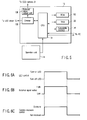
- FIG. 5 shows a schematic configuration of the controller 13. Like elements shown in FIG. 2 are designated by like reference numerals.
- an external signal output unit 136 is connected to the dimmer 135.
- the external signal output unit 136 outputs a TTL level signal serving as a control signal of the CCD camera 21 in accordance with an instruction for turning ON/OFF the LED 4 from the CPU 131.
- the external signal output unit 136 outputs a high level when the LED 4 is turned ON, and outputs a low level when the LED 4 is turned OFF.
- An output signal from the external signal output unit 136 is inputted to the exposure control signal input terminal of the CCD camera 21 via a cable (not shown).
- the CCD camera 21 is set to an exposure standby state by the camera controller (not shown).
- the CPU 131 detects a push operation of the button 142; reads out an operation angle (rotation angle) of the dimmer dial 143; and outputs to the dimmer 135 the dimmer indicator value according to the operation angle.
- the dimmer 135 outputs an electric power indicator signal which corresponds to the dimmer indicator value to the LED driver 12, and turns ON the LED 4 at the brightness (luminous flux) which corresponds to the dimmer indicator value (FIG. 6A). At the same time, the dimmer 135 outputs an electric power indicator signal to the external signal output unit 136.
- the external signal output unit 136 generates a high level signal by turning ON the LED 4 (FIG. 6B), and outputs the generated signal to the exposure control signal input terminal of the CCD camera 21. In this manner, the CCD camera 21 having received the high level input signal from the external signal output unit 136 starts exposure (FIG. 6C).
- the CPU 131 detects a release operation of the button 142; determines a turning OFF instruction; and outputs a turning OFF signal to the dimmer 135. Having received this signal, the dimmer 135 outputs the turning OFF signal to the LED driver 12, and turns OFF the LED 4 (FIG. 6A). In addition, the dimmer 135 outputs the turning OFF signal to the external signal output unit 136.
- the external signal output unit 136 generates a low level signal by turning OFF the LED 4 (FIG. 6B), and outputs the generated signal to the external control signal input terminal of the CCD camera 21. In this manner, the CCD camera 21 having received the low level input signal from the external signal output unit 136 ends exposure (FIG. 6C).
- the high/low level signal is outputted at the same time as when the LED 4 is turned ON/OFF by operation of the button 142 on the operation unit 14.
- an auxiliary button is provided on the operation unit 14, whereby enabling/disabling of an output of a high/low level signal corresponding to turning ON/OFF the LED 4 may be controlled by operation of the auxiliary button.
- the output of the high/low level signal corresponding to turning ON/OFF the LED 4 is enabled, it is possible to employ a control such that operation of the dimmer dial 143 is disabled.
- undesired dimming during exposure of the CCD camera 21 can be prevented in advance.
- FIG. 7 is a diagram showing a schematic configuration of a microscope system using a microscope fluorescence illumination apparatus according to the third embodiment of the invention. Like elements shown in FIG. 1 are designated by like reference numerals.
- a CCD camera 22 having an exposure control signal output terminal is allocated in a photography optical path split by the beam splitter 9.
- the CCD camera 22 outputs a TTL level signal from the exposure control signal output terminal in accordance with an exposure control state.
- a high level signal is outputted from the exposure control signal output terminal.
- a low level signal is outputted therefrom.
- the CCD camera 22 according to the embodiment can notify another device of the exposure control state.
- a signal from the exposure control signal output terminal of the CCD camera 22 is inputted to the controller 13 via a cable (not shown).
- FIG. 8 is a diagram showing a schematic configuration of the controller 13. Like elements shown in FIG. 2 are designated by like reference numerals.
- an external signal input unit 137 which receives a TTL level of an instruction input command according to an operating state of the CCD camera 22 is connected to the dimmer 135.
- the dimmer 135 turns ON/OFF the LED 4 in response to the instruction input signal of the external signal input unit 137.
- the LED 4 is turned ON.
- the LED 4 is turned OFF.
- the dimmer 135 turns ON/OFF the LED 4 via the LED driver 12 in accordance with an instruction for turning ON/OFF the LED 4 from the CPU 131 regardless of the instruction input signal of the external signal input unit 137. Further, the dimmer 135 is designed to adjust a power variable signal for the LED driver 12 and increase or decrease the illumination luminous flux by the LED 4 in accordance with a dimming instruction from the CPU 131.
- the CPU 131 reads out an operation angle of the dimmer dial 143 and outputs to the dimmer a dimmer indicator value which corresponds thereto.
- the dimmer 135 outputs to the LED driver 12 a power indicator signal which corresponds to the dimmer indicator value and turns ON the LED 4 at the brightness (luminous flux) which corresponds to the dimmer indicator value. In this case, the dimmer 135 holds the dimmer indicator value.
- the CPU 131 detects the push operation of the button 142 and enables the dimmer 135 to turn OFF the LED and the external signal input unit 137 to capture the instruction input signal.
- the dimmer 135 turns OFF the LED 4 via the LED driver 12 and enters a standby state of the instruction input signal for the external signal input unit 137.
- a low level signal is generated from the exposure control signal output terminal, and the fact is notified to the external signal input unit 137 (FIG. 9A).
- the dimmer 135 turns OFF the LED 4 via the LED driver 12 in response to the low level signal from the external signal input unit 137 (FIG. 9B).
- excitation light is emitted to the fluorescence sample S only while exposure is carried out by the CCD camera 22.
- emission can be carried out smoothly without any problem and minimum excitation light emission can be achieved as required.
- FIG. 10 is a diagram showing a schematic configuration of a microscope system using a microscope fluorescence illumination apparatus according to the fourth embodiment of the invention. Like elements shown in FIG. 1 are designated by like reference numerals.
- an LED 31 as well as the LED 4 is allocated as an illumination light source.
- the LED 31 has a light emitting main wavelength which is different from the LED 4.
- a condenser 32 and a dichroic mirror 33 are allocated in an optical path of the light emitted from the LED 31.
- the condenser 32 converts the light emitted from the LED 31 into parallel light beams.
- the dichroic mirror 33 is provided at a position at which the optical path of the light emitted from the LED 1 and the optical path of the light emitted from the LED 4 intersect against each other.
- the dichroic mirror 33 has a feature of reflecting the wavelength light from the LED 31 and transmitting the wavelength light from the LED 4.
- the controller 13 is connected to the LED 31 via an LED driver 34.
- the LED driver 34 controls turning ON/OFF of the LED 31 in accordance with an instruction supplied from the controller 13.
- a CCD camera 35 having an exposure control signal output terminal is allocated on an optical path for photography split by the beam splitter 9.
- the CCD camera 35 outputs a TTL level signal from the exposure control signal output terminal in accordance with an exposure control state.
- a high level signal is outputted from the exposure control signal output terminal.
- a low level signal is outputted therefrom.
- the CCD camera 35 can notify another device of the exposure control state.
- the CCD camera 35 is provided as a fully pixel readout interline type CCD high speed camera. The camera enables exposure of several milliseconds at an exposure data transfer time of some tens of microseconds and repetition continuous image pickup.
- a signal from the exposure control signal output terminal of the CCD camera 35 is inputted to the controller 13 via a cable (not shown).
- FIG. 11 is a diagram showing a schematic configuration of the controller 13. Like elements shown in FIG. 2 are designated by like reference numerals.
- an external signal input unit 138 which receives an indicator input signal (TTL level) according to the operating state of the CCD camera 35 is connected to the dimmer 135.
- the LED driver 12 and an LED driver 34 are connected to the dimmer 135, so that the LED 4 and the LED 31 can be turned ON/OFF in response to the indicator input signal from the external signal input unit 138.
- the dimmer 135 having received the dimmer indicator value from the CPU 131 outputs to the LED driver 12 and the LED driver 34 the pulse width modulation (PWM) waveform which corresponds to this dimmer indicator value.
- PWM pulse width modulation
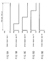
- the PWM cycle is 250 microseconds and a duty (ratio between high level and low level of PWM cycle) can be varied in accordance with the dimmer indicator value in units of 2.5 microseconds.
- the PWM waveform duty as shown in FIGS. 13A to 13E can be obtained in accordance with the dimmer indicator value.
- the LED driver 12 supplies a current Ia to the LED 4 only while the PWM waveform inputted from the dimmer 135 is at a high level and interrupts the current Ia while it is at a low level.
- the current Ia is preset to the LED driver 12 and is adjusted in accordance with a feature of the LED 4. By varying a time during which the current Ia is thus supplied, the luminous flux radiated from the LED 4 is varied, and the excitation light illumination from the LED 4 is dimmed.
- the LED driver 34 also supplies a current Ib to the LED 31 only while the PWM waveform inputted from the dimmer 135 is at a high level and interrupts the current Ib while it is at a low level.
- the current Ib is also preset to the LED driver 34 and adjusted in accordance with a feature of the LED 31. By varying a time at which the current Ib is thus supplied, the luminous flux radiated from the LED 31 is varied and the excitation light illumination from the LED 31 is dimmed.
- the operation unit 14 serving as a man-machine interface is connected to the controller 13 configured as described above.
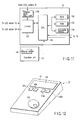
- FIG. 12 is a view showing a schematic configuration of the operation unit 14. Like elements shown in FIG. 3 are designated by like reference numerals.
- the operation unit 14 is allocated on the surface of the operation unit main body 141.
- the operation unit comprises four buttons 142a, 142b, 142c, 142d which form an operating input unit, and further, comprises an LCD 144 serving as a display unit.
- the buttons 142a, 142b, 142c, 142d each outputs an operation signal according to a push operation or a release operation. These operation signals can be read out by the CPU 131.
- the button 142a turns ON/OFF the LED 4.
- the button 142b turns ON/OFF the LED 31.
- the button 142c selects an LED targeted for dimming. Dimming objects of the dimmer dial 143 are toggle-selected as the LED 4, the LED 31, the LED 4, ... every time the button 142c is operated.
- the button 142d toggle-switches two control modes, i.e., a normal mode and a two-wavelength excitation mode described later every time the button is operated.
- the LCD 144 displays various kinds of setting information or operation information in accordance with an instruction from the CPU 131. Then, the CPU 131 having received an operation signal from the operation unit 14 controls each unit in response to the operation signal.
- the CPU 131 detects this operation.
- the CPU 131 reads out an operation angle (rotation angle) of the dimmer dial 143 and outputs to the dimmer 135 the dimmer indicator value according to the operation angle.
- the dimmer 135 outputs the PWM waveform according to the dimmer indicator value to the LED driver 12 and turns ON the LED 4 at the brightness (luminous flux) which corresponds to the dimmer indicator value.
- the CPU 131 outputs to the dimmer 135 "100" which is the maximum dimmer indicator value.
- the dimmer 135, as shown in FIG. 13C outputs to the LED driver 12 the PWM waveform when all the periods of the PWN cycle are at a high level. In this manner, the LED 4 radiates the maximum luminous flux specified by the supply current Ia and carries out the brightest excitation light illumination for the fluorescence sample S.
- the CPU 131 detects this operation; outputs to the dimmer 135 a switch signal of a dimming target; and switches the dimming target from the LED 4 to the LED 31.
- the CPU 131 reads out an operation angle (rotation angle) of the dimmer dial 143 and outputs to the dimmer 135 the dimmer indicator value according to the operation angle.
- the dimmer 135 outputs to the LED driver 34 the PWM waveform according to the dimmer indicator value and turns ON the LED 31 at the brightness (luminous flux) which corresponds to the dimmer indicator value.
- the CPU 131 when the dimmer dial 143 is set at an intermediate operation angle, the CPU 131 outputs to the dimmer 135 "50" which is the intermediate dimmer indicator value.
- the dimmer 135 outputs to the LED driver 34 the PWM waveform when a period which is half of the PWM cycle is at a high level, as shown in FIG. 13C. In this manner, the LED 31 radiates half of the maximum luminous flux specified by the supply current Ia and carries out excitation light illumination for the fluorescence sample S at the brightness which is half of the maximum brightness.
- the CPU 131 detects this operation and switches the normal mode to the two-wavelength excitation mode.
- the CPU 131 outputs a signal indicating the two-waveform excitation mode to the dimmer 135.
- the dimmer 135 fixes a current level to a low level based on the PWM waveform outputs to the LED driver 12 and the LED driver 34 while holding the dimmer indicator values of the LED 4 and the LED 31. In this manner, both of the LED 4 and the LED 31 are turned OFF, and the excitation input illumination for the fluorescence sample S is eliminated. Then, the dimmer 135 enters an instruction input signal standby state for the external signal input unit 138.
- a high level signal is outputted from the exposure control signal output terminal, and the outputted signal is sent to the external signal input unit 138.
- the dimmer 135 outputs the PWM waveform (PWM waveform corresponding to the held dimmer indicator value) to the LED driver 12 immediately due to input of the high level signal to the external signal input unit 138 (refer to FIG. 14B). In this manner, the PWM waveform is outputted to the LED driver in synchronization with the input of the high level signal to the external signal input unit 138, and the excitation light illumination by the LED 4 is started.
- a low level signal is outputted from the exposure control signal output terminal of the CCD camera 35 and the CCD camera 35 starts transfer and readout of the first image.
- the low level signal outputted from the exposure control signal output terminal of the CCD camera 35 is sent to the external signal input unit 138.
- the dimmer 135 outputs the PWM waveform (all the periods of the PWM cycle are at a low level) to the LED driver 12 due to input of the low level signal to the external signal input unit 138. In this manner, the low level signal is outputted to the LED driver 12 in synchronization with the input of the low level signal of the external signal input unit 138, and the excitation light illumination by the LED 4 is turned OFF.
- the CCD camera 35 is also connected to an image acquisition board (not shown).
- the image acquisition board is mounted on a PC (not shown) via a PCI bus or the like. In this manner, the CCD camera 35 transfers the read-out image data to the PC.
- next exposure is enabled.
- the CCD camera 35 starts a second exposure (refer to a second exposure period shown in FIG. 14A)
- a high level signal is outputted from the exposure control signal output terminal and the outputted signal is sent to the external signal input unit 138.
- the dimmer 135 outputs the PWM waveform (PWM waveform corresponding to the held dimmer indicator value) to the LED driver 34 immediately due to input of the high level signal to the external signal input unit 138 (refer to FIG. 14B).
- the PWM waveform is outputted to the LED driver 34 in synchronization with the input of the high level signal to the external signal input unit 138, and the excitation light illumination by the LED 31 is started.
- the dimmer 135 outputs the PWM waveform (when all the periods of the PWM cycle are at a low level) to the LED driver 12 immediately due to input of the low level signal to the external signal input unit 138. In this manner, the low level signal is outputted to the LED driver 12 in synchronization with the input of the low level signal to the external signal input unit 138, and the excitation light illumination by the LED 4 is turned OFF.
- the CCD camera 35 is also connected to an image acquisition board, although not shown.
- the image acquisition board is mounted on a PC, although not shown, via a PCI bus or the like.
- image transfer by the CCD camera 35 is terminated (within some tens of microseconds in a fast case), next exposure is enabled.
- the CCD camera 35 starts a second exposure (refer to a period of the second exposure shown in FIG. 14A)
- a high level signal is outputted from the exposure control signal outputted terminal, and the outputted signal is sent to the external signal input unit 138.
- the dimmer 135 outputs the PWM waveform (PWM waveform corresponding to the held dimmer indicator value) to the LED driver 34 by inputting the high level signal to the external signal input unit 138 (refer to FIG. 14B). In this manner, the PWM waveform is outputted to the LED driver 34 in synchronization with the input of the high level signal to the external signal input unit 138 and the excitation light illumination by the LED 31 is started.
- PWM waveform PWM waveform corresponding to the held dimmer indicator value
- a low level signal is outputted from the exposure control output terminal of the CCD camera 35 and the CCD camera 35 starts transfer and readout of a second image.
- the low level signal outputted from the exposure control signal output terminal of the CCD camera 35 is sent to the external signal input unit 138.
- the dimmer 135 outputs the PWM waveform (when all the periods of the PWM cycle are at a low level) to the LED driver 34 immediately due to input of the low level signal to the external signal input unit 138 (refer to FIG. 14B). In this manner, the low level signal is outputted to the LED driver 34 in synchronization with the input of the low level signal of the external signal input unit 138, and the excitation light illumination by the LED 31 is turned OFF.
- the CCD camera 35 transfers the read-out image data to the PC.
- next exposure is enabled.
- the CCD camera 35 starts a third exposure (refer to a period of third exposure shown in FIG. 14A)
- a high level signal is outputted from the exposure control signal output terminal and the outputted signal is sent to the external signal input unit 138.
- the dimmer 135 outputs the PWM waveform (PWM waveform corresponding to the held dimmer indicator value) to the LED driver 12 immediately due to input of the high level signal to the external signal input unit 138.
- the low level signal is outputted to the LED driver 12 in synchronization with the input of the high level signal of the external signal input unit 138, and the excitation light illumination by the LED 4 is started.
- the above-described operation is then repeated until the exposure count set at the camera controller (not shown) of the CCD camera 35 has been terminated.
- a fluorescence image of the fluorescence sample S due to the excitation light illumination of the LED 4 is acquired during exposure in odd numbered shot of the CCD camera 35.
- a fluorescence image of the fluorescence sample S due to the excitation light illumination of the LED 31 is acquired during exposure in even numbered shot of the CCD camera 35.
- the apparatus according to the fourth embodiment configured as described above is applied to two-wavelength ratio imaging in which Fura 2 has been introduced as calcium ion concentration measurement.
- an LED having a light emitting main wavelength of 340 nm and an LED having a light emitting main wavelength of 380 nm are used for the LED 4 and the LED 31, respectively.
- the switching of these two types of excitation light beams (340 nm and 380 nm) is carried out by using an exposure control signal output from the CCD camera 35. In this manner, there can be achieved two-wavelength switching in order of microseconds which have been conventionally impossible in a mechanical configuration such as a high speed shutter or a high speed filter wheel.
- PWM control which is a dimming control can be started in synchronization with the start of each exposure of the CCD camera 35.
- the acquired image by each exposure can be obtained as a stable fluorescence image without any distortion or instability in excitation light illumination.
- a ratio having good precision can be obtained.
- the required minimum excitation light illumination is achieved for the fluorescence sample S.
- the damage to a living cell can be remarkably reduced than conventionally, enabling observation or fluorescence imaging of the living cell for a long time.
- the apparatus of the present invention has a command set including a plurality of control commands. Therefore, by using an external communication unit (not shown) and transmitting and receiving the command set by a proper application on the PC, a GUI application can achieve a further integrated, sophisticated fluorescence imaging work environment.
- a microscope fluorescence illumination apparatus having excellence in sample protection, operability, and power saving, in which emission of the excitation light can be carried out only during the required minimum period during observation or photography in fluorescence observation by using a solid-state illumination device as a light source for illumination of the fluorescence observation.
Applications Claiming Priority (2)
| Application Number | Priority Date | Filing Date | Title |
|---|---|---|---|
| JP2004137439A JP2005321453A (ja) | 2004-05-06 | 2004-05-06 | 顕微鏡用蛍光照明装置 |
| JP2004137439 | 2004-05-06 |
Publications (2)
| Publication Number | Publication Date |
|---|---|
| EP1593996A2 true EP1593996A2 (de) | 2005-11-09 |
| EP1593996A3 EP1593996A3 (de) | 2006-10-11 |
Family
ID=34936045
Family Applications (1)
| Application Number | Title | Priority Date | Filing Date |
|---|---|---|---|
| EP05009607A Withdrawn EP1593996A3 (de) | 2004-05-06 | 2005-05-02 | Beleuchtungs-Anordnung für die Fluoreszenz-Mikroskopie |
Country Status (3)
| Country | Link |
|---|---|
| US (1) | US20050248839A1 (de) |
| EP (1) | EP1593996A3 (de) |
| JP (1) | JP2005321453A (de) |
Cited By (8)
| Publication number | Priority date | Publication date | Assignee | Title |
|---|---|---|---|---|
| WO2008022139A2 (en) | 2006-08-14 | 2008-02-21 | Westover Scientific, Inc. | Solid state fluorescence light assembly and microscope |
| DE102007007798A1 (de) | 2007-02-16 | 2008-08-21 | Leica Microsystems Cms Gmbh | Fluoreszenz-Beleuchtungseinrichtung |
| DE102007007797A1 (de) | 2007-02-16 | 2008-08-28 | Leica Microsystems Cms Gmbh | Fluoreszenzmikroskop mit Beleuchtungseinrichtung |
| CZ299772B6 (cs) * | 2008-02-06 | 2008-11-19 | Sieger@Ladislav | Zpusob pulzního buzení LED diod s odstranením stroboskopického jevu |
| DE102008045671A1 (de) * | 2008-09-03 | 2010-03-04 | Bundesrepublik Deutschland, vertreten durch den Präsidenten der Bundesanstalt für Geowissenschaften und Rohstoffe | Fluoreszenz-Mikroskop, insbesondere für Gesteinsuntersuchungen |
| US8233039B2 (en) | 2007-06-06 | 2012-07-31 | Olympus Corporation | Microscope image pickup system |
| JP2013050613A (ja) * | 2011-08-31 | 2013-03-14 | Nikon Corp | 顕微鏡システムおよび制御プログラム |
| DE102016109945A1 (de) | 2015-11-05 | 2017-05-11 | Leica Microsystems Cms Gmbh | Mikroskop für die Durchlicht- und Fluoreszenzmikroskopie |
Families Citing this family (18)
| Publication number | Priority date | Publication date | Assignee | Title |
|---|---|---|---|---|
| DE102005049378A1 (de) * | 2005-10-12 | 2007-04-19 | Carl Zeiss Jena Gmbh | Automatisches Mikroskop |
| US7846391B2 (en) | 2006-05-22 | 2010-12-07 | Lumencor, Inc. | Bioanalytical instrumentation using a light source subsystem |
| US8098375B2 (en) | 2007-08-06 | 2012-01-17 | Lumencor, Inc. | Light emitting diode illumination system |
| JP5108490B2 (ja) | 2007-12-19 | 2012-12-26 | オリンパス株式会社 | 細胞解析装置用照明装置 |
| WO2010027000A1 (ja) * | 2008-09-03 | 2010-03-11 | オリンパス株式会社 | 顕微鏡及び顕微鏡の制御方法 |
| US8242462B2 (en) | 2009-01-23 | 2012-08-14 | Lumencor, Inc. | Lighting design of high quality biomedical devices |
| CN101943794A (zh) * | 2010-07-30 | 2011-01-12 | 苏州生物医学工程技术研究所 | 一种荧光显微镜 |
| CN102566025A (zh) * | 2010-12-09 | 2012-07-11 | 苏州生物医学工程技术研究所 | 一种保持视场光照度一致的显微镜 |
| CN102566024A (zh) * | 2010-12-09 | 2012-07-11 | 苏州生物医学工程技术研究所 | 一种使用触摸屏系统控制光源的荧光显微镜 |
| US8389957B2 (en) | 2011-01-14 | 2013-03-05 | Lumencor, Inc. | System and method for metered dosage illumination in a bioanalysis or other system |
| US8466436B2 (en) | 2011-01-14 | 2013-06-18 | Lumencor, Inc. | System and method for metered dosage illumination in a bioanalysis or other system |
| JP5875812B2 (ja) * | 2011-09-27 | 2016-03-02 | オリンパス株式会社 | 顕微鏡システムおよび照明強度調整方法 |
| US8967811B2 (en) | 2012-01-20 | 2015-03-03 | Lumencor, Inc. | Solid state continuous white light source |
| KR101172840B1 (ko) | 2012-05-21 | 2012-08-09 | 주식회사디에치엠 | 현미경용 조광장치 |
| US9217561B2 (en) | 2012-06-15 | 2015-12-22 | Lumencor, Inc. | Solid state light source for photocuring |
| HU231246B1 (hu) * | 2015-08-31 | 2022-05-28 | 3Dhistech Kft | Konfokális elvû tárgylemez szkenner |
| JP6688189B2 (ja) * | 2016-08-09 | 2020-04-28 | オリンパス株式会社 | 顕微鏡装置 |
| CN106990519A (zh) * | 2017-05-12 | 2017-07-28 | 中国科学院苏州生物医学工程技术研究所 | 结构光照明显微成像系统 |
Citations (4)
| Publication number | Priority date | Publication date | Assignee | Title |
|---|---|---|---|---|
| US6154282A (en) * | 1998-10-26 | 2000-11-28 | Cytotelesis Inc. | Semiconductor based excitation illuminator for fluorescence and phosphorescence microscopy |
| EP1186882A2 (de) * | 2000-09-07 | 2002-03-13 | Leica Microsystems Heidelberg GmbH | Verfahren und Vorrichtung zur Detektion von Fluoreszenzlicht bei der konfokalen Rastermikroskopie |
| JP2002350732A (ja) * | 2001-05-25 | 2002-12-04 | Nikon Corp | 蛍光観察装置 |
| JP2003195177A (ja) * | 2001-12-27 | 2003-07-09 | Nikon Corp | 照明光照射装置及びこれを備えた蛍光観察装置 |
Family Cites Families (4)
| Publication number | Priority date | Publication date | Assignee | Title |
|---|---|---|---|---|
| MX9200720A (es) * | 1992-02-21 | 1993-09-01 | Invest Y Centro | Mejoras a microscopio metalografico util para la caracterizacion de dados de estirado de conductores. |
| US6400502B1 (en) * | 1998-08-18 | 2002-06-04 | Nikon Corporation | Microscope |
| JP2002131648A (ja) * | 2000-10-20 | 2002-05-09 | Olympus Optical Co Ltd | 蛍光顕微鏡 |
| JP2003262797A (ja) * | 2002-03-11 | 2003-09-19 | Olympus Optical Co Ltd | 顕微鏡システム |
-
2004
- 2004-05-06 JP JP2004137439A patent/JP2005321453A/ja active Pending
-
2005
- 2005-04-28 US US11/118,585 patent/US20050248839A1/en not_active Abandoned
- 2005-05-02 EP EP05009607A patent/EP1593996A3/de not_active Withdrawn
Patent Citations (4)
| Publication number | Priority date | Publication date | Assignee | Title |
|---|---|---|---|---|
| US6154282A (en) * | 1998-10-26 | 2000-11-28 | Cytotelesis Inc. | Semiconductor based excitation illuminator for fluorescence and phosphorescence microscopy |
| EP1186882A2 (de) * | 2000-09-07 | 2002-03-13 | Leica Microsystems Heidelberg GmbH | Verfahren und Vorrichtung zur Detektion von Fluoreszenzlicht bei der konfokalen Rastermikroskopie |
| JP2002350732A (ja) * | 2001-05-25 | 2002-12-04 | Nikon Corp | 蛍光観察装置 |
| JP2003195177A (ja) * | 2001-12-27 | 2003-07-09 | Nikon Corp | 照明光照射装置及びこれを備えた蛍光観察装置 |
Non-Patent Citations (2)
| Title |
|---|
| PATENT ABSTRACTS OF JAPAN vol. 2003, no. 04, 2 April 2003 (2003-04-02) & JP 2002 350732 A (NIKON CORP), 4 December 2002 (2002-12-04) * |
| PATENT ABSTRACTS OF JAPAN vol. 2003, no. 11, 5 November 2003 (2003-11-05) & JP 2003 195177 A (NIKON CORP), 9 July 2003 (2003-07-09) * |
Cited By (13)
| Publication number | Priority date | Publication date | Assignee | Title |
|---|---|---|---|---|
| EP2057496A2 (de) * | 2006-08-14 | 2009-05-13 | Westover Scientific, Inc. | Festkörperbaugruppe mit fluoreszierendem licht und mikroskop |
| WO2008022139A2 (en) | 2006-08-14 | 2008-02-21 | Westover Scientific, Inc. | Solid state fluorescence light assembly and microscope |
| EP2057496A4 (de) * | 2006-08-14 | 2010-07-07 | Westover Scient Inc | Festkörperbaugruppe mit fluoreszierendem licht und mikroskop |
| US8922885B2 (en) | 2007-02-16 | 2014-12-30 | Leica Microsystems Cms Gmbh | Fluorescence microscope having an illumination device |
| DE102007007797A1 (de) | 2007-02-16 | 2008-08-28 | Leica Microsystems Cms Gmbh | Fluoreszenzmikroskop mit Beleuchtungseinrichtung |
| DE102007007798A1 (de) | 2007-02-16 | 2008-08-21 | Leica Microsystems Cms Gmbh | Fluoreszenz-Beleuchtungseinrichtung |
| DE102007007797B4 (de) * | 2007-02-16 | 2017-11-16 | Leica Microsystems Cms Gmbh | Fluoreszenzmikroskop mit Beleuchtungseinrichtung |
| US8233039B2 (en) | 2007-06-06 | 2012-07-31 | Olympus Corporation | Microscope image pickup system |
| CZ299772B6 (cs) * | 2008-02-06 | 2008-11-19 | Sieger@Ladislav | Zpusob pulzního buzení LED diod s odstranením stroboskopického jevu |
| DE102008045671A1 (de) * | 2008-09-03 | 2010-03-04 | Bundesrepublik Deutschland, vertreten durch den Präsidenten der Bundesanstalt für Geowissenschaften und Rohstoffe | Fluoreszenz-Mikroskop, insbesondere für Gesteinsuntersuchungen |
| JP2013050613A (ja) * | 2011-08-31 | 2013-03-14 | Nikon Corp | 顕微鏡システムおよび制御プログラム |
| DE102016109945A1 (de) | 2015-11-05 | 2017-05-11 | Leica Microsystems Cms Gmbh | Mikroskop für die Durchlicht- und Fluoreszenzmikroskopie |
| US10429630B2 (en) | 2015-11-05 | 2019-10-01 | Leica Microsystems Cms Gmbh | Microscope for transmitted-light and fluorescence microscopy |
Also Published As
| Publication number | Publication date |
|---|---|
| EP1593996A3 (de) | 2006-10-11 |
| JP2005321453A (ja) | 2005-11-17 |
| US20050248839A1 (en) | 2005-11-10 |
Similar Documents
| Publication | Publication Date | Title |
|---|---|---|
| EP1593996A2 (de) | Beleuchtungs-Anordnung für die Fluoreszenz-Mikroskopie | |
| EP1553436B1 (de) | Fluoreszenzmikroskop mit LED-Lichtquelle und Steuereinheit zur Synchronisierung der Bildaufzeichnung mit dem Ein- und Ausschalten der Lichtquelle | |
| US7229202B2 (en) | Light-emitting diode illumination system for an optical observation device, in particular a stereomicroscope or stereo surgical microscope | |
| CN102573212B (zh) | 照明单元和内窥镜装置 | |
| US9810895B2 (en) | Biological observation apparatus | |
| US8699138B2 (en) | Multi-wavelength multi-lamp radiation sources and systems and apparatuses incorporating same | |
| EP1780574B1 (de) | Mikroskopsystem mit einer Beleuchtungsvorrichtung | |
| EP2248458A1 (de) | Beleuchtungsvorrichtung und endoskopsystem | |
| JP6044941B2 (ja) | 光学顕微鏡、および、光学顕微鏡のオートフォーカス装置 | |
| US8344652B2 (en) | Optical measuring apparatus | |
| WO2019202828A1 (ja) | 内視鏡システムおよび蛍光画像出力方法 | |
| US11076106B2 (en) | Observation system and light source control apparatus | |
| JP2005345716A (ja) | 顕微鏡 | |
| US20140313577A1 (en) | Method for illuminating an object in a digital light microscope, digital light microscope and bright field reflected-light illumination device for a digital light microscope | |
| JP2007068699A (ja) | 光源装置 | |
| US20050259437A1 (en) | Apparatus, systems and methods relating to illumination for microscopes | |
| JP2002102142A (ja) | 蛍光内視鏡装置および蛍光内視鏡システム | |
| JP2002350732A (ja) | 蛍光観察装置 | |
| JP5108490B2 (ja) | 細胞解析装置用照明装置 | |
| JP2005091701A (ja) | 蛍光顕微鏡及び蛍光顕微鏡の励起光源制御方法 | |
| CN112043240A (zh) | 用于荧光诊断的光源、系统和用于荧光诊断的方法 | |
| US10151908B2 (en) | Image acquisition device and image acquisition method | |
| Whoriskey | LEDs in Microscopy: An Emerging Research Tool | |
| Hohman | LED Light Source: Major Advance in Fluorescence Microscopy | |
| JP2006030280A (ja) | 顕微鏡用照明装置、方法およびコンピュータプログラム |
Legal Events
| Date | Code | Title | Description |
|---|---|---|---|
| PUAI | Public reference made under article 153(3) epc to a published international application that has entered the european phase |
Free format text: ORIGINAL CODE: 0009012 |
|
| AK | Designated contracting states |
Kind code of ref document: A2 Designated state(s): AT BE BG CH CY CZ DE DK EE ES FI FR GB GR HU IE IS IT LI LT LU MC NL PL PT RO SE SI SK TR |
|
| AX | Request for extension of the european patent |
Extension state: AL BA HR LV MK YU |
|
| PUAL | Search report despatched |
Free format text: ORIGINAL CODE: 0009013 |
|
| AK | Designated contracting states |
Kind code of ref document: A3 Designated state(s): AT BE BG CH CY CZ DE DK EE ES FI FR GB GR HU IE IS IT LI LT LU MC NL PL PT RO SE SI SK TR |
|
| AX | Request for extension of the european patent |
Extension state: AL BA HR LV MK YU |
|
| AKX | Designation fees paid | ||
| STAA | Information on the status of an ep patent application or granted ep patent |
Free format text: STATUS: THE APPLICATION IS DEEMED TO BE WITHDRAWN |
|
| 18D | Application deemed to be withdrawn |
Effective date: 20070412 |
|
| REG | Reference to a national code |
Ref country code: DE Ref legal event code: 8566 |