EP1593126B1 - Mram-architektur für niedrige stromaufnahme und hohe selektivität - Google Patents
Mram-architektur für niedrige stromaufnahme und hohe selektivität Download PDFInfo
- Publication number
- EP1593126B1 EP1593126B1 EP04702030A EP04702030A EP1593126B1 EP 1593126 B1 EP1593126 B1 EP 1593126B1 EP 04702030 A EP04702030 A EP 04702030A EP 04702030 A EP04702030 A EP 04702030A EP 1593126 B1 EP1593126 B1 EP 1593126B1
- Authority
- EP
- European Patent Office
- Prior art keywords
- current
- magnetoresistive memory
- memory cell
- line
- bridging element
- Prior art date
- Legal status (The legal status is an assumption and is not a legal conclusion. Google has not performed a legal analysis and makes no representation as to the accuracy of the status listed.)
- Expired - Lifetime
Links
- 230000015654 memory Effects 0.000 claims abstract description 138
- 238000000034 method Methods 0.000 claims abstract description 14
- 239000011159 matrix material Substances 0.000 claims abstract description 11
- 238000004519 manufacturing process Methods 0.000 claims abstract description 4
- 238000000926 separation method Methods 0.000 claims description 41
- 239000002184 metal Substances 0.000 claims description 32
- 230000008901 benefit Effects 0.000 abstract description 8
- 239000010410 layer Substances 0.000 description 70
- 230000005291 magnetic effect Effects 0.000 description 50
- 238000004364 calculation method Methods 0.000 description 12
- 239000004020 conductor Substances 0.000 description 11
- 230000005415 magnetization Effects 0.000 description 11
- 239000010408 film Substances 0.000 description 9
- 241001581440 Astroides Species 0.000 description 8
- 230000004888 barrier function Effects 0.000 description 8
- 238000010586 diagram Methods 0.000 description 7
- 239000000463 material Substances 0.000 description 5
- 230000006399 behavior Effects 0.000 description 4
- 230000008859 change Effects 0.000 description 4
- 230000005293 ferrimagnetic effect Effects 0.000 description 4
- 230000005294 ferromagnetic effect Effects 0.000 description 4
- 239000011229 interlayer Substances 0.000 description 4
- 230000005641 tunneling Effects 0.000 description 4
- 230000000694 effects Effects 0.000 description 3
- 238000000059 patterning Methods 0.000 description 3
- 230000000295 complement effect Effects 0.000 description 2
- 230000001419 dependent effect Effects 0.000 description 2
- 238000009826 distribution Methods 0.000 description 2
- 230000010287 polarization Effects 0.000 description 2
- 238000003860 storage Methods 0.000 description 2
- 229910017107 AlOx Inorganic materials 0.000 description 1
- 229910003321 CoFe Inorganic materials 0.000 description 1
- 229910001030 Iron–nickel alloy Inorganic materials 0.000 description 1
- 230000005290 antiferromagnetic effect Effects 0.000 description 1
- 238000003491 array Methods 0.000 description 1
- 239000002131 composite material Substances 0.000 description 1
- 230000008094 contradictory effect Effects 0.000 description 1
- 238000000151 deposition Methods 0.000 description 1
- 238000005516 engineering process Methods 0.000 description 1
- 230000006870 function Effects 0.000 description 1
- 239000012212 insulator Substances 0.000 description 1
- 239000000696 magnetic material Substances 0.000 description 1
- 239000007769 metal material Substances 0.000 description 1
- 230000008569 process Effects 0.000 description 1
- 230000009467 reduction Effects 0.000 description 1
- 239000004065 semiconductor Substances 0.000 description 1
- 230000003068 static effect Effects 0.000 description 1
- 239000010409 thin film Substances 0.000 description 1
- 238000004804 winding Methods 0.000 description 1
Images


Classifications
-
- G—PHYSICS
- G11—INFORMATION STORAGE
- G11C—STATIC STORES
- G11C11/00—Digital stores characterised by the use of particular electric or magnetic storage elements; Storage elements therefor
- G11C11/02—Digital stores characterised by the use of particular electric or magnetic storage elements; Storage elements therefor using magnetic elements
- G11C11/14—Digital stores characterised by the use of particular electric or magnetic storage elements; Storage elements therefor using magnetic elements using thin-film elements
- G11C11/15—Digital stores characterised by the use of particular electric or magnetic storage elements; Storage elements therefor using magnetic elements using thin-film elements using multiple magnetic layers
-
- H—ELECTRICITY
- H10—SEMICONDUCTOR DEVICES; ELECTRIC SOLID-STATE DEVICES NOT OTHERWISE PROVIDED FOR
- H10N—ELECTRIC SOLID-STATE DEVICES NOT OTHERWISE PROVIDED FOR
- H10N52/00—Hall-effect devices
- H10N52/80—Constructional details
Definitions
- the present invention relates to magnetic or magnetoresistive random access memories (MRAMs), and more particularly to an MRAM architecture that allows low power consumption and high selectivity during writing as well as methods of operating the same.
- MRAMs magnetic or magnetoresistive random access memories
- MRAM Magnetic or Magnetoresistive Random Access Memory
- SRAM static RAM
- the MRAM concept was originally developed at Honeywell Corp. USA, and uses magnetization direction in a magnetic multilayer device as information storage and the resultant resistance difference for information readout. As with all memory devices, each cell in an MRAM array must be able to store at least two states which represent either a "1" or a "0".
- MR magnetoresistive
- GMR Giant Magneto-Resistance
- TMR Tunnel Magneto-Resistance
- MTJ Magnetic Tunnel Junction
- SDT Spin Dependent Tunneling
- the effective in-plane resistance of the composite multilayer structure is smallest when the magnetization directions of the films are parallel and largest when the magnetization directions of the films are anti-parallel. If a thin dielectric interlayer is placed between two ferromagnetic or ferrimagnetic films, tunneling current between the films is observed to be the largest (or thus resistance to be the smallest) when the magnetization directions of the films are parallel and tunneling current between the films is the smallest (or thus resistance the largest) when the magnetization directions of the films are anti-parallel.
- Magneto-resistance is usually measured as a percentage increase in resistance of the above structures going from parallel to anti-parallel magnetization states. TMR devices provide higher percentage magneto-resistance than GMR structures, and thus have the potential for higher signals and higher speed. Recent results indicate tunneling giving over 40% magneto-resistance, compared to 10-14% magneto-resistance in good GMR cells.
- a typical MRAM device comprises a plurality of magnetoresistive memory elements, e.g. MTJ elements, arranged in an array.
- MTJ memory elements generally include a layered structure comprising a fixed or pinned layer, a free layer and a dielectric barrier in between.
- the pinned layer of magnetic material has a magnetic vector that always points in the same direction.
- the magnetic vector of the free layer is free, but constrained within the easy axis of the layer, which is determined chiefly by the physical dimensions of the element.
- the magnetic vector of the free layer points in either of two directions: parallel or anti-parallel with the magnetization direction of the pinned layer, which coincides with the said easy axis.
- Word lines extend along rows of memory elements, and bit lines extend along columns of memory elements.
- the word lines and bit lines are patterned separately into two metal layers under and above the MTJ stack.
- Each memory element is located at a cross-point region of a word line and a bit line.
- the bit lines are, for example, parallel with the hard axis of the memory elements, which creates a magnetic field in the direction of the easy axis, while the word lines are then parallel with the easy axis of the memory elements, which creates a magnetic field in the direction of the hard axis.
- Writing is done by simultaneously applying current pulses through the bit and the word lines that intersect at a selected cell.
- a peak magnetic field is generated, sufficient to switch the polarization of the free layer of the MTJ element, so as to switch the resistance of the MTJ element from the LoRes (low resistance) state to the HiRes (high resistance) state or vice versa (depending on the direction of the current through the bit line).
- the currents in the selected word line and the selected bit line are such that only together they provide a magnetic field able to change the direction of the magnetic vector of the free layer of the selected memory element, but the current in either line by itself is not able to change the storage state.
- the direction of the resultant magnetic field makes an angle of 45° with respect to the easy axis of the free layer of the cell. At this angle, the switching field of the free layer is the smallest, as shown by the astroid curve in Fig. 1 , thus writing can be done with the least current in both lines.
- the magnitude of the resultant magnetic field at the crossing point is:
- the end point of the field vector applied to the magnetoresistive element must be on or outside the astroid curve in order to switch the magnetization of the free layer.
- the currents in the selected bit line and word line must be chosen in such a way that the total field sufficiently exceeds the switching field of the addressed cell at 45° with the easy axis, or in other words, so that the end of the resultant field vector is on or outside the astroid branch in this direction (see Fig. 1 ).
- the magnitude of the field created by only the bit line itself must be significantly smaller than the switching fields in the easy axis direction of any of the cells lying on the same bit line to prevent undesired over-writing.
- H s-min and H s-max are the permitted minimum and maximum switching fields of the free layer in the easy axis direction.
- the distribution width of the switching field must be well confined within these two values.
- the selectivity window is represented by the shaded area in Fig. 2 . This means the astroid curves of all cells must be well confined within this area.
- One problem of the conventional design is that the selectivity is rather low. It is technically difficult to fabricate millions of cells with narrow distribution in switching field because the variation in sizes of tunnel junction elements can be rather significant with small structures.
- a disadvantage with conventional MRAM devices is that the method to create magnetic field with a straight conductor is the most ineffective way.
- the programming current needed is high, because of the requirement of two high enough magnetic fields being induced in the neighborhood of the magnetoresistive material.
- the field is created equally at any point along the line, but only at the intersection point it is actually used.
- 0.6 ⁇ m CMOS technology proves to give stable read and write operations using currents in the 5 to 10 mA range. Typical devices in these demonstrations were about 0.1 to 0.5 ⁇ m 2 .
- Magnetic fields are created on-chip by sending a current through bit or word lines, in general called current lines, and are proportional to the current. For obtaining higher magnetic fields, higher currents need to be used. However, low power applications will require low currents. Those are contradictory requirements. It would be advantageous to obtain higher selectivity while using lower currents.
- the magnetic field generated by current in either conductor alone, or the combined magnetic field generated by current in two of those conductors, is not strong enough to change the magnetization orientation of the selected memory cell.
- This solution although improving the selectivity, does not really reduce the power consumption, as current needs to be sent through more current lines.
- US 5,734,606 discloses the provision of new types of memory cell structures for a magnetic random access memory.
- a memory cell has a plurality of cell pieces where digital information is stored. Each cell piece is formed by magnetic layers separated by a conductor layer.
- a word line is placed adjacent each cell piece for winding around cell pieces and meandering on a same plane on cell pieces, for example. The invention attains less power consumption and effective usage for a word current.
- the present invention provides a magnetoresistive memory cell, comprising a magnetoresistive memory element, a first current line and a second current line, the first and the second current line crossing each other at a cross-point region but not being in direct contact.
- a bridging element connects the first and the second current line in the vicinity of the cross-point region, and the bridging element is magnetically couplable to the magnetoresistive memory element.
- the bridging element comprises at least a first component which lies in a plane parallel to the first and second current lines and at least one second component which is perpendicular thereto.
- the first component may be for example a strip patterned in a metal layer
- the second component may be for example a via or a plug.
- the bridging element comprises one first component and two second components, the bridging element may be U-shaped. This has the advantage that the magnetic field created by current flowing through the U-shaped bridging element is enhanced and concentrated at the magnetoresistive element, if this magnetoresistive element is placed at the center point of the bridging element.
- the bridging element comprises one first component and only one second component, the bridging element may be L-shaped. The field created by current flowing through these first and second components is used for switching the magnetization direction of the memory element during writing.
- the resultant field orientation of the bridging element may be in any direction, but preferably is in-plane and at an angle such that the switching field of the free layer is the smallest, for example, at an angle of 45° from the easy axis of the free layer of the memory element.
- the bridging element may be a conductive structure, so that current can flow through it, in order to generate the necessary magnetic field to write a value in the magnetoresistive element.
- a magnetoresistive memory cell according to the present invention may comprise a separation device between the bridging element and the first current line or between the bridging element and the second current line.
- a magnetoresistive memory cell according to the present invention may comprise a separation device in between components of the bridging element, for example in between the first component and the second component or one of the second components.
- the separation device if present, must be somewhere in the current path between the first and the second current line.
- An advantage of such separation device is that it blocks sneak currents (i.e. currents flowing through alternate, undesired current paths) in unselected bridging elements, but does not block current in selected bridging elements.
- the separation device may have a symmetrical and non-linear current-voltage characteristic, i.e. it is a bi-directionally conducting non-linear device.
- An advantage thereof is that it allows to write in two directions (generation of magnetic fields in two directions).
- the separation device may comprise a sandwich of conductive material, barrier material and conductive material.
- the conductive material may be a metal material.
- the barrier material may be an insulator material or a semiconductor material.
- an n/p+/n structure or an n+/n-/p+/n-/n+ structure, or their complementary forms, can also be used as a separation device.
- the above-mentioned structures provide a symmetrical non-linear current-voltage characteristic, and any other structure that also provides such symmetrical non-linear current-voltage characteristic can also be used. When current is sent in any of two opposite direction through the separation device, the device has a symmetrical behavior.
- the bridging element may have a center point, i.e. a point which is equidistant from all components of the bridging element.
- the magnetoresistive memory element may be located at the center point of the bridging element. This has the advantage that the generated magnetic field is concentrated at the memory element.
- the memory element may be located as close as possible to all components of the bridging element. By locating the magnetoresistive memory element at the center point of the bridging element, or as close as possible to all components of the bridging element, it may be located completely outside the cross-point region of the first and second current lines.
- the present invention also provides a matrix of magnetoresistive memory cells comprising magnetoresitive memory cells according to the present invention.
- the magnetoresistive memory cells are linked together to form logically organized rows and columns. Each row is provided with a first current line and each column is provided with a second current line.
- the first and the second current lines cross each other at cross-point regions, wherein the bridging elements connect the first and second current lines in the vicinity of the cross-point regions and the bridging elements are magnetically couplable to the magnetoresistive memory elements.
- Every memory cell of the matrix of magnetoresistive memory cells may be provided with a selection transistor, i.e. the memory cells are of the 1T1MTJ type. This allows for a faster reading, a larger signal and less noise.
- every row of memory cells may be provided with a sense line.
- the memory cells do not include selection transistors, i.e. they are of the 0T1MTJ type, and thus may have a smaller intrinsic cell size.
- the present invention furthermore provides a method of use of a magnetoresistive memory cell according to the invention in a process of writing a value in a matrix of magnetoresistive memory cells, each magnetoresistive memory cell comprising a magnetoresistive memory element, the magnetoresistive memory cells being linked together to form logically organized rows and columns, each row being provided with a first current line and each column being provided with a second current line, the first and the second current lines crossing each other at cross-point regions in the memory cells, each memory cell being provided with a bridging element conductively connecting the first current line and the second current line.
- the method comprises the steps of sending a current through a selected first current line, sending a current through a selected bridging element and sending a current through a selected second current line.
- the bridging element may conductively connect the first current line and the second current line through a separation device, the method of use then furthermore comprising sending current through a separation device.
- the present invention furthermore provides a method of manufacturing a magnetoresistive memory cell according to the invention.
- the method comprises forming a first current line in a first metal layer, forming a second current line in a second metal layer, forming a first component of a bridging element in a third metal layer, and forming at least one second component of the bridging element by means of intermetal interconnects.
- the manufacturing method may furthermore comprise forming a separation device between the bridging element and any of the first or second current line, or in between the bridging element components.
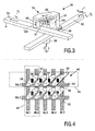
- a matrix 40 of magnetoresistive memory cells 30 (see Fig. 4 ), each memory cell 30 comprising a magnetoresistive memory element 31, is logically organized in rows 41 and columns 42.
- the terms “horizontal” and “vertical” are used to provide a co-ordinate system and for ease of explanation only. They do not need to, but may, refer to an actual physical direction of the device.
- the terms “column” and “row” are used to describe sets of array elements which are linked together. The linking can be in the form of a Cartesian array of rows and columns; however, the present invention is not limited thereto.
- rows and columns can be easily interchanged and it is intended in this disclosure that these terms be interchangeable.
- non-Cartesian arrays may be constructed and are included within the scope of the invention. Accordingly the terms “row” and “column” should be interpreted widely. To facilitate in this wide interpretation, the claims refer to logically organized rows and columns. By this is meant that sets of memory elements are linked together in a topologically linear intersecting manner; however, that the physical or topographical arrangement need not be so.
- the rows may be circles and the columns may be radii of these circles and the circles and radii are described in this invention as "logically organized" in rows and columns.
- specific names of the various lines e.g.
- bit line and word line, or row line and column line are intended to be generic names used to facilitate the explanation and to refer to a particular function and this specific choice of words is not intended to in any way limit the invention. It should be understood that all these terms are used only to facilitate a better understanding of the specific structure being described, and are in no way intended to limit the invention.
- One memory cell 30 according to an embodiment of the present invention is represented in Fig. 3 .
- An architecture according to the present invention may use an orthogonal grid of bit lines 32 (patterned in a first metal layer) and word lines 33 (patterned in a second metal layer).
- an architecture according to the present invention may use a grid of bit lines and word lines, where the bit lines and word lines include an angle different from 90°, as e.g. in US-2002/0097601 .
- the embodiment with the bit lines and word lines including an angle of 90° is preferred as it leads to the smallest cell size.
- the word lines may be in the first metal layer and the bit lines may be in the second metal layer, i.e.
- word lines are provided in a metal layer above the metal layer of the bit lines, or vice versa.
- the word lines 33 and bit lines 32 intersect at an intersection region or cross-point region, i.e. a zone where they cross or overlap each other without being in direct contact (as they are made in different metal layers).
- a U-shaped bridge 34 is formed which connects the bit line 32 and the word line 33 in the vicinity of the intersection region.
- the bridge 34 comprises a plurality of components, e.g. bridge 34 consists of a first component formed by a first via 35, a second component formed by a top bar 36 (patterned in a third metal layer) and a third component formed by a second via 37.
- a separation device 38 which serves as a separator to block sneak currents flowing through undesired paths.
- the separation device may be located in between via 35 and word line 33. The separation device must be provided in the current path between the word line 33 and the bit line 32.
- the separation device may be provided in between bridge components, e.g. between the first via 35 and the top bar 36, or between the second via 37 and the top bar 36.
- the top bar 36 is oriented under an angle, such as e.g. 45°, with the bit line 32 and the word line 33.
- the angle is such that the normal of the bridge plane, i.e. the plane formed by the bridge components 35, 36, 37, is oriented at an angle at which the switching field is the minimum.
- the magnetoresistive memory element 31, e.g. MTJ stack, is located at the center of the U-shaped bridge 34, in between the second and the third metal layer, i.e. at a level which is higher than both the level of the bit line 32 and of the word line 33.
- the magnetoresistive memory element may be placed in between the first and the second metal layer, i.e.
- this embodiment is less preferred, as less magnetic field generated by current flowing through the bridging element is sensed in the magnetic memory element, as it is further away from the top bar 36 and first via 35. In fact the magnetic field at the magnetic memory element is substantially only formed by the current in the second via 37.
- Fig. 3 The above arrangement, as represented in Fig. 3 is just an example, as indicated by the alternatives already given. Furthermore, the whole structure as drawn in Fig. 3 can be turned upside down, which means that the top bar 36 can be physically located at the bottom of the device, underneath the metal layers wherein the bit line and word line are formed.
- MTJ memory element 31 generally includes a layered structure comprising a fixed or pinned layer, a free layer and a dielectric barrier in between.
- the MTJ memory element 31 furthermore comprises a non-magnetic conductor forming a lower electrical contact or bottom electrode, and an upper contact or top electrode on e.g. the free magnetic layer.
- the stack of free and pinned layers can also be reversed, so that the upper contact is on the pinned magnetic layer.
- the pinned magnetic layer and the free magnetic layer may be composed of e.g. NiFe or CoFe and the dielectric barrier layer may e.g. be made of AlOx.
- both free and pinned layers can be formed by a multilayer of different magnetic layers, also in combination with non-magnetic or antiferromagnetic layers.
- the magnetoresistive element 31 is located outside the cross-point region of the bit line 32 and word line 33, i.e. outside the zone where bit line 32 and word line 33 cross each other. Because underneath the magnetoresistive memory element 31, e.g. MTJ stack, there is no conductive or metal line, a third via 39 can be placed there to connect the bottom electrode of the magnetoresistive memory element 31 down to a selection transistor T for read operation.
- the top electrode of the magnetoresistive element 31, e.g. MTJ stack is in contact with the top bar 36.
- FIG. 4 A top view of the proposed architecture is shown in Fig. 4 , and a side view is shown in Fig. 5 .
- the area of the separation device 38 in each cell 30 can be extended as much as possible, as long as it does not touch the third via 39 and the separation devices 38 of the neighboring cells 30.
- a binary value i.e. e.g. a "1” or a "0"
- V write is applied on one end of the corresponding bit line 32, as shown in Fig. 3 .
- a current pulse I w will flow from the bit line 32, through the separation device 38, the second via 37, top bar 36, first via 35 and finally through the word line 33 to the ground. This is also shown in Fig. 6 .
- the current partly forms a loop which creates a magnetic field H according to the right hand rule.
- the field is oriented with respect to the easy axis at an angle which is the same as the angle included between the top bar 36 of the bridge 34 and the bit line 32 or word line 33, e.g. at 45°, due to the orientation of the bridge 34 with respect to the bit line 32 and the word line 33.
- the field strength is chosen in such a way that it exceeds the switching field of the free layer at that angle. Due to the shape of the bridge 34, the field created by the write current I w is enhanced and concentrated to the selected memory element 31. Writing in another direction is done by sending the current in the opposite direction. The current can hardly escape to other paths through unselected cells thanks to the separation devices 38.
- a separation device may consist of a sandwich structure of metal-barrier-metal, such as metal-insulator-metal, or metal-semiconductor-metal, as described in US-6331944 .
- the separation devices are deposited and patterned on top of the bit lines 32 or on top of the word lines 33.
- the separation device 38 can provide a non-linear current-voltage (I-V) characteristic which is symmetrical with respect to the origin.
- Fig. 7 shows the positive part of such an I-V curve according to US-6331944 .
- the current through the separation device 38 at a bias of V B (about 1 Volt) is more than ten times larger than that at a bias of 1/2 V B . Therefore, the write current I w in Fig.
- the separation device 38 should have a symmetrical I-V characteristic, i.e. it should be a bi-directionally conducting non-linear device, because in order to be able to write in both directions (i.e. generating magnetic field in both directions), the device must have symmetrical behaviors when the current is sent in any of the opposite directions.
- a symmetrical I-V characteristic i.e. it should be a bi-directionally conducting non-linear device, because in order to be able to write in both directions (i.e. generating magnetic field in both directions), the device must have symmetrical behaviors when the current is sent in any of the opposite directions.
- other structures that also provide a symmetrical non-linear behaviors such as an n/p + /n structure and an n + /n - /p + /n - /n + structures and their complementary forms are also possible, as also mentioned in US-5991193 .
- Reading of the content of memory element 31 is done in a manner similar to conventional designs.
- a sense current is sent via a selected word line 33, first via 35, top bar 36 of the bridge 34, through the magnetoresistive memory element 31, e.g. MTJ stack, third via 39 and ends up in the selection transistor T, which is now in the ON state.
- the architecture of the memory cells according to the present invention allows to obtain sufficient write field with significantly less current. This is because the total write field is a sum of fields created by three segments 35, 36, 37 of the U-shaped bridge 34 and this total field is already oriented in the direction of minimum switching field, e.g. at 45° with respect to the easy axis of the magnetoresistive element 31.
- the power consumption is further reduced because only one current pulse instead of two is sent during writing, the same current flowing through both the bit line 32 and the word line 33.
- the current I w has to flow through only half of the bit line 32 and word line 33, which can reduce some resistance of the lines 32, 33.
- the following rough calculations show that the present invention offers much power consumption reduction.
- only one current I w is needed, while in the conventional design, two currents I 1 , I 2 are needed.
- a schematic circuit diagram of an array of 100 by 100 cells is simplified and shown in Fig. 10 .
- the resistors R select and R unselect are resistances of the separation devices 38 at the selected and unselected memory cells 30. Because R unselect is biased at half voltage of that on R select , according to the non-linear behavior of the separation device 38, it can be supposed that R unselect is for instance 12.5*R select .
- the resistance R select is set approximately to R line , which is practically reasonable.
- the sneak paths mainly go through all unselected memory cells 30 directly connected to the selected bit line 32 and word line 33. All other memory cells 30 are considered shorted.
- Selectivity of the architecture of embodiments of the present invention is significantly higher than that of the conventional one. This is due to the fact that the write field is concentrated only at the U-shaped bridge 34 and oriented under 45° with respect to the easy axis, at which the switching field is the lowest.
- the field created by a selected bit line 32, but applied to unselected cells lying on the same bit line 32 is very small because the bit line 32 is deeply buried under the magnetoresistive element 31, e.g. MTJ stack, and this field is oriented at 0° with respect to the easy axis, at which the switching field is the highest. The following calculations reveal more.
- This field is quite small because the bit line 32 is buried rather far away from the free layer 80 of the magnetoresistive memory element 31, e.g. MTJ stack, (in the calculation, see also Fig. 6 , 1450 nm is supposed to be the vertical distance between the free layer 80 and the bit line 32).
- the perpendicular component is negligibly smaller and certainly plays no important rule due to the large sheet anisotropy of the free layer 80.
- This field is created by sneak currents flowing through the U-shaped bridge 34, therefore it is 12.5 times smaller than the field created at the selected memory cell 30.
- the U-shaped bridge 34 still has very low self-inductance, which will not affect the high frequency performance of the magnetoresistive memory. Rough calculations show that the inductance of the bridge 34, excluding the straight part of the conduction line, is about 10 -13 - 10 -11 H. This value is still about two orders of magnitude smaller than that of a single-turn recording head, which can operate at 1 GHz without problems.
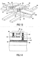
- FIG. 13 An alternative embodiment of a device according to the present invention is shown in Fig. 13 .
- the architecture of this embodiment is basically the same as the first embodiment shown in Fig. 3 .
- the difference is that there is no selection transistor T for every memory 30 cell. Therefore, the third via 39 as in Fig. 3 is not present.
- a sense line 130 is patterned into the conductive layer underneath the bottom electrode of the magnetoresistive memory element 31.
- the sense line 130 connects the bottom electrodes of all magnetoresistive memory elements 31 lying on the same word line 33 with each other.
- each sense line 130 is associated with a row of magnetoresistive memory elements 31, just like a word line 33 is.
- the separation device 38 is now again, during read-out, connected in series with the magnetoresistive memory element 31, such as e.g. an MTJ, and can act to block sneak currents during reading, as described above.
- Reading for instance of the cell i th , is carried out by sending a sense current through the sense line 130 associated with selected memory cell i th , through the magnetoresistive memory element 31 of cell i th , through the top bar 36, the second via 37, the separation device 38, and finally it goes out via bit line 32 associated with the selected memory cell i th .
- This sense current will sense the resistance of the memory cell i th , or thus of the memory element 31 of that cell, and the digital state of the memory cell i th can be detected.
- a third embodiment is similar to the second one. The difference is how the separation devices 38 are made. Instead of depositing a sandwich film of metal-barrier-metal and patterning it, in the current embodiment a continuous barrier layer 140 is deposited on the polished surface of bit lines 32, and then without patterning, second via's 37 are created on top of the barrier layer 140 ( Fig. 14 ). In this case, the bit lines 32 and second via's 37 act as the two metal electrodes of the structure metal-barrier-metal. With this design, an extra mask for patterning the separation devices 38 can be omitted.
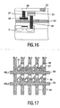
- bridging element 34 is an L-shaped bridge, i.e. it comprises as a first component top bar 36, lying in a plane which is parallel to the plane of the word line 33 or bit line 32, and as a second component via 37, perpendicular to top bar 36.
- the top bar 36 is patterned in the same level or same metal layer as the word line 33.
- the magnetoresistive memory element e.g. MTJ element 31, is placed in between the 1 st and the 2 nd metal layer, being the metal layers in which the bit lines 32 and the word lines 33 have been patterned.
- the magnetic field generated at the MTJ element 31 is smaller than the magnetic field created with the devices of the other embodiments, because in this case, the magnetic field is created by only 2 segments of the bridging element 34: via 37 and top bar 36.
- the combination of the device according to the fourth embodiment with the teaching of the second embodiment can be applied. That means that a sense line can be put underneath the MTJ element 31 for use when reading.
- the separation device 38 might be located just underneath the top bar 36 of the bridging element 34, at the upper end of via 37.
Landscapes
- Engineering & Computer Science (AREA)
- Computer Hardware Design (AREA)
- Semiconductor Memories (AREA)
- Mram Or Spin Memory Techniques (AREA)
- Hall/Mr Elements (AREA)
Claims (13)
- Magnetoresistive Speicherzelle (30), umfassend: ein magnetoresistives Speicherelement (31), eine erste Stromleitung (32) und eine zweite Stromleitung (33), wobei sich die erste und die zweite Stromleitung (32, 33) an einem Kreuzungspunktbereich kreuzen, jedoch nicht in direktem Kontakt stehen, dadurch gekennzeichnet, dass ein Überbrückungselement (34) die erste und die zweite Stromleitung (32, 33) in der Nähe des Kreuzungspunktbereichs verbindet, das Überbrückungselement (34) mit dem magnetoresistiven Speicherelement (31) magnetisch koppelbar ist und wobei das Überbrückungselement (34) umfasst: mindestens eine erste Komponente (36), die ein einer Ebene parallel zur ersten und zweiten Stromleitung liegt, und eine zweite Komponente (35, 37), die rechtwinklig dazu ist.
- Magnetoresistive Speicherzelle (30) nach Anspruch 1, wobei das Überbrückungselement (34) eine leitende Struktur ist.
- Magnetoresistive Speicherzelle (30) nach Anspruch 1, wobei eine Trennungsvorrichtung (38) zwischen dem Überbrückungselement (34) und der ersten Stromleitung (32) oder zwischen dem Überbrückungselement (34) und der zweiten Stromleitung (33) vorhanden ist.
- Magnetoresistive Speicherzelle (30) nach Anspruch 1, wobei eine Trennungsvorrichtung (38) zwischen Komponenten des Überbrückungselements (34) vorhanden ist.
- Magnetoresistive Speicherzelle (30) nach Anspruch 3 oder 4, wobei die Trennungsvorrichtung (38) eine nichtlineare Strom-Spannungs-Kennlinie aufweist.
- Magnetoresistive Speicherzelle (30) nach Anspruch 5, wobei die Trennungsvorrichtung (38) eine symmetrische nichtlineare Strom-Spannungs-Kennlinie aufweist.
- Magnetoresistive Speicherzelle (30) nach Anspruch 1, wobei das Überbrückungselement (34) einen Mittelpunkt aufweist, wobei das magnetoresistive Speicherelement (31) am Mittelpunkt des Überbrückungselements (34) befindlich ist.
- Matrix magnetoresistiver Speicherzellen, die magnetoresistive Speicherzellen nach einem der vorangehenden Ansprüche umfasst, wobei die magnetoresistiven Speicherzellen (30) miteinander verbunden sind, so dass sie logisch organisierte Reihen (41) und Spalten (42) ausbilden, wobei jede Reihe (41) mit einer ersten Stromleitung (32) versehen ist und jede Spalte (42) mit einer zweiten Stromleitung (33) versehen ist, wobei sich die ersten und die zweiten Stromleitungen (32, 33) an Kreuzungspunktbereichen kreuzen, wobei die Überbrückungselemente die ersten und die zweiten Stromleitungen in der Nähe der Kreuzungspunktbereiche verbinden und die Überbrückungselemente mit den magnetoresistiven Speicherelementen magnetisch koppelbar sind.
- Matrix nach Anspruch 8, wobei jede Speicherzelle mit einem Auswahltransistor versehen ist.
- Matrix nach Anspruch 8, wobei jede Reihe von Speicherzellen mit einer Abfrageleitung (130) versehen ist.
- Verfahren zum Schreiben eines Werts in eine Matrix magnetoresistiver Speicherzellen nach Anspruch 1, wobei das Verfahren folgende Schritte umfasst: Senden eines Stroms durch eine ausgewählte erste Stromleitung, Senden eines Stroms durch ein ausgewähltes Überbrückungselement (34) und Senden eines Stroms durch eine ausgewählte zweite Stromleitung.
- Verfahren zur Verwendung einer magnetoresistiven Speicherzelle nach Anspruch 11, wobei das Verfahren ferner das Senden von Strom durch eine Trennungsvorrichtung (38) umfasst.
- Verfahren zur Herstellung einer magnetoresistiven Speicherzelle nach Anspruch 1, das Folgendes umfasst: Ausbilden einer ersten Stromleitung in einer ersten Metallschicht, Ausbilden einer zweiten Stromleitung in einer zweiten Metallschicht, Ausbilden einer ersten Komponente eines Überbrückungselements in einer dritten Metallschicht und Ausbilden mindestens einer zweiten Komponente des Überbrückungselements mithilfe von Metall-Metall-Verbindungen.
Priority Applications (1)
| Application Number | Priority Date | Filing Date | Title |
|---|---|---|---|
| EP04702030A EP1593126B1 (de) | 2003-01-31 | 2004-01-14 | Mram-architektur für niedrige stromaufnahme und hohe selektivität |
Applications Claiming Priority (4)
| Application Number | Priority Date | Filing Date | Title |
|---|---|---|---|
| EP03100211 | 2003-01-31 | ||
| EP03100211 | 2003-01-31 | ||
| PCT/IB2004/050022 WO2004068498A1 (en) | 2003-01-31 | 2004-01-14 | Mram architecture for low power consumption and high selectivity |
| EP04702030A EP1593126B1 (de) | 2003-01-31 | 2004-01-14 | Mram-architektur für niedrige stromaufnahme und hohe selektivität |
Publications (2)
| Publication Number | Publication Date |
|---|---|
| EP1593126A1 EP1593126A1 (de) | 2005-11-09 |
| EP1593126B1 true EP1593126B1 (de) | 2009-03-25 |
Family
ID=32799005
Family Applications (1)
| Application Number | Title | Priority Date | Filing Date |
|---|---|---|---|
| EP04702030A Expired - Lifetime EP1593126B1 (de) | 2003-01-31 | 2004-01-14 | Mram-architektur für niedrige stromaufnahme und hohe selektivität |
Country Status (9)
| Country | Link |
|---|---|
| US (1) | US7277317B2 (de) |
| EP (1) | EP1593126B1 (de) |
| JP (1) | JP4932471B2 (de) |
| KR (1) | KR101009891B1 (de) |
| CN (1) | CN100505086C (de) |
| AT (1) | ATE426898T1 (de) |
| DE (1) | DE602004020186D1 (de) |
| TW (1) | TWI323890B (de) |
| WO (1) | WO2004068498A1 (de) |
Families Citing this family (89)
| Publication number | Priority date | Publication date | Assignee | Title |
|---|---|---|---|---|
| JPWO2006030516A1 (ja) | 2004-09-17 | 2008-05-08 | 富士通株式会社 | 磁気記憶装置及びその製造方法 |
| JP2007027415A (ja) * | 2005-07-15 | 2007-02-01 | Toshiba Corp | 磁気記憶装置 |
| US7786460B2 (en) | 2005-11-15 | 2010-08-31 | Macronix International Co., Ltd. | Phase change memory device and manufacturing method |
| US7450411B2 (en) * | 2005-11-15 | 2008-11-11 | Macronix International Co., Ltd. | Phase change memory device and manufacturing method |
| US7635855B2 (en) | 2005-11-15 | 2009-12-22 | Macronix International Co., Ltd. | I-shaped phase change memory cell |
| US7414258B2 (en) | 2005-11-16 | 2008-08-19 | Macronix International Co., Ltd. | Spacer electrode small pin phase change memory RAM and manufacturing method |
| US7449710B2 (en) | 2005-11-21 | 2008-11-11 | Macronix International Co., Ltd. | Vacuum jacket for phase change memory element |
| US7459717B2 (en) | 2005-11-28 | 2008-12-02 | Macronix International Co., Ltd. | Phase change memory cell and manufacturing method |
| US7688619B2 (en) | 2005-11-28 | 2010-03-30 | Macronix International Co., Ltd. | Phase change memory cell and manufacturing method |
| US7531825B2 (en) | 2005-12-27 | 2009-05-12 | Macronix International Co., Ltd. | Method for forming self-aligned thermal isolation cell for a variable resistance memory array |
| US8062833B2 (en) | 2005-12-30 | 2011-11-22 | Macronix International Co., Ltd. | Chalcogenide layer etching method |
| US7741636B2 (en) | 2006-01-09 | 2010-06-22 | Macronix International Co., Ltd. | Programmable resistive RAM and manufacturing method |
| US7560337B2 (en) | 2006-01-09 | 2009-07-14 | Macronix International Co., Ltd. | Programmable resistive RAM and manufacturing method |
| US7554144B2 (en) | 2006-04-17 | 2009-06-30 | Macronix International Co., Ltd. | Memory device and manufacturing method |
| US7928421B2 (en) * | 2006-04-21 | 2011-04-19 | Macronix International Co., Ltd. | Phase change memory cell with vacuum spacer |
| US7423300B2 (en) * | 2006-05-24 | 2008-09-09 | Macronix International Co., Ltd. | Single-mask phase change memory element |
| US7696506B2 (en) * | 2006-06-27 | 2010-04-13 | Macronix International Co., Ltd. | Memory cell with memory material insulation and manufacturing method |
| US7785920B2 (en) | 2006-07-12 | 2010-08-31 | Macronix International Co., Ltd. | Method for making a pillar-type phase change memory element |
| US7772581B2 (en) | 2006-09-11 | 2010-08-10 | Macronix International Co., Ltd. | Memory device having wide area phase change element and small electrode contact area |
| US7504653B2 (en) | 2006-10-04 | 2009-03-17 | Macronix International Co., Ltd. | Memory cell device with circumferentially-extending memory element |
| US7863655B2 (en) | 2006-10-24 | 2011-01-04 | Macronix International Co., Ltd. | Phase change memory cells with dual access devices |
| US7476587B2 (en) | 2006-12-06 | 2009-01-13 | Macronix International Co., Ltd. | Method for making a self-converged memory material element for memory cell |
| US7903447B2 (en) | 2006-12-13 | 2011-03-08 | Macronix International Co., Ltd. | Method, apparatus and computer program product for read before programming process on programmable resistive memory cell |
| US7718989B2 (en) | 2006-12-28 | 2010-05-18 | Macronix International Co., Ltd. | Resistor random access memory cell device |
| US7619311B2 (en) | 2007-02-02 | 2009-11-17 | Macronix International Co., Ltd. | Memory cell device with coplanar electrode surface and method |
| US7884343B2 (en) | 2007-02-14 | 2011-02-08 | Macronix International Co., Ltd. | Phase change memory cell with filled sidewall memory element and method for fabricating the same |
| US7956344B2 (en) | 2007-02-27 | 2011-06-07 | Macronix International Co., Ltd. | Memory cell with memory element contacting ring-shaped upper end of bottom electrode |
| US7786461B2 (en) | 2007-04-03 | 2010-08-31 | Macronix International Co., Ltd. | Memory structure with reduced-size memory element between memory material portions |
| US8610098B2 (en) | 2007-04-06 | 2013-12-17 | Macronix International Co., Ltd. | Phase change memory bridge cell with diode isolation device |
| US7796421B2 (en) * | 2007-05-08 | 2010-09-14 | Magsil Corporation | Programmable magnetic read only memory (MROM) |
| TWI402980B (zh) | 2007-07-20 | 2013-07-21 | Macronix Int Co Ltd | 具有緩衝層之電阻式記憶結構 |
| US7884342B2 (en) | 2007-07-31 | 2011-02-08 | Macronix International Co., Ltd. | Phase change memory bridge cell |
| US7729161B2 (en) | 2007-08-02 | 2010-06-01 | Macronix International Co., Ltd. | Phase change memory with dual word lines and source lines and method of operating same |
| US7642125B2 (en) | 2007-09-14 | 2010-01-05 | Macronix International Co., Ltd. | Phase change memory cell in via array with self-aligned, self-converged bottom electrode and method for manufacturing |
| US8178386B2 (en) | 2007-09-14 | 2012-05-15 | Macronix International Co., Ltd. | Phase change memory cell array with self-converged bottom electrode and method for manufacturing |
| US7919766B2 (en) | 2007-10-22 | 2011-04-05 | Macronix International Co., Ltd. | Method for making self aligning pillar memory cell device |
| US7646631B2 (en) | 2007-12-07 | 2010-01-12 | Macronix International Co., Ltd. | Phase change memory cell having interface structures with essentially equal thermal impedances and manufacturing methods |
| US7879643B2 (en) | 2008-01-18 | 2011-02-01 | Macronix International Co., Ltd. | Memory cell with memory element contacting an inverted T-shaped bottom electrode |
| US7879645B2 (en) | 2008-01-28 | 2011-02-01 | Macronix International Co., Ltd. | Fill-in etching free pore device |
| US8158965B2 (en) | 2008-02-05 | 2012-04-17 | Macronix International Co., Ltd. | Heating center PCRAM structure and methods for making |
| US8084842B2 (en) | 2008-03-25 | 2011-12-27 | Macronix International Co., Ltd. | Thermally stabilized electrode structure |
| US8030634B2 (en) | 2008-03-31 | 2011-10-04 | Macronix International Co., Ltd. | Memory array with diode driver and method for fabricating the same |
| US7825398B2 (en) | 2008-04-07 | 2010-11-02 | Macronix International Co., Ltd. | Memory cell having improved mechanical stability |
| US7791057B2 (en) | 2008-04-22 | 2010-09-07 | Macronix International Co., Ltd. | Memory cell having a buried phase change region and method for fabricating the same |
| US8077505B2 (en) | 2008-05-07 | 2011-12-13 | Macronix International Co., Ltd. | Bipolar switching of phase change device |
| US7701750B2 (en) | 2008-05-08 | 2010-04-20 | Macronix International Co., Ltd. | Phase change device having two or more substantial amorphous regions in high resistance state |
| US8415651B2 (en) | 2008-06-12 | 2013-04-09 | Macronix International Co., Ltd. | Phase change memory cell having top and bottom sidewall contacts |
| US8134857B2 (en) | 2008-06-27 | 2012-03-13 | Macronix International Co., Ltd. | Methods for high speed reading operation of phase change memory and device employing same |
| US7932506B2 (en) | 2008-07-22 | 2011-04-26 | Macronix International Co., Ltd. | Fully self-aligned pore-type memory cell having diode access device |
| US7903457B2 (en) | 2008-08-19 | 2011-03-08 | Macronix International Co., Ltd. | Multiple phase change materials in an integrated circuit for system on a chip application |
| US7719913B2 (en) | 2008-09-12 | 2010-05-18 | Macronix International Co., Ltd. | Sensing circuit for PCRAM applications |
| US8324605B2 (en) | 2008-10-02 | 2012-12-04 | Macronix International Co., Ltd. | Dielectric mesh isolated phase change structure for phase change memory |
| US7897954B2 (en) | 2008-10-10 | 2011-03-01 | Macronix International Co., Ltd. | Dielectric-sandwiched pillar memory device |
| US8036014B2 (en) * | 2008-11-06 | 2011-10-11 | Macronix International Co., Ltd. | Phase change memory program method without over-reset |
| US8664689B2 (en) | 2008-11-07 | 2014-03-04 | Macronix International Co., Ltd. | Memory cell access device having a pn-junction with polycrystalline plug and single-crystal semiconductor regions |
| US8907316B2 (en) | 2008-11-07 | 2014-12-09 | Macronix International Co., Ltd. | Memory cell access device having a pn-junction with polycrystalline and single crystal semiconductor regions |
| US7869270B2 (en) | 2008-12-29 | 2011-01-11 | Macronix International Co., Ltd. | Set algorithm for phase change memory cell |
| US8089137B2 (en) | 2009-01-07 | 2012-01-03 | Macronix International Co., Ltd. | Integrated circuit memory with single crystal silicon on silicide driver and manufacturing method |
| US8107283B2 (en) | 2009-01-12 | 2012-01-31 | Macronix International Co., Ltd. | Method for setting PCRAM devices |
| US8030635B2 (en) | 2009-01-13 | 2011-10-04 | Macronix International Co., Ltd. | Polysilicon plug bipolar transistor for phase change memory |
| US8064247B2 (en) | 2009-01-14 | 2011-11-22 | Macronix International Co., Ltd. | Rewritable memory device based on segregation/re-absorption |
| US8933536B2 (en) | 2009-01-22 | 2015-01-13 | Macronix International Co., Ltd. | Polysilicon pillar bipolar transistor with self-aligned memory element |
| US8084760B2 (en) | 2009-04-20 | 2011-12-27 | Macronix International Co., Ltd. | Ring-shaped electrode and manufacturing method for same |
| US8173987B2 (en) | 2009-04-27 | 2012-05-08 | Macronix International Co., Ltd. | Integrated circuit 3D phase change memory array and manufacturing method |
| US8097871B2 (en) | 2009-04-30 | 2012-01-17 | Macronix International Co., Ltd. | Low operational current phase change memory structures |
| US7933139B2 (en) | 2009-05-15 | 2011-04-26 | Macronix International Co., Ltd. | One-transistor, one-resistor, one-capacitor phase change memory |
| US7968876B2 (en) | 2009-05-22 | 2011-06-28 | Macronix International Co., Ltd. | Phase change memory cell having vertical channel access transistor |
| US8350316B2 (en) | 2009-05-22 | 2013-01-08 | Macronix International Co., Ltd. | Phase change memory cells having vertical channel access transistor and memory plane |
| US8809829B2 (en) | 2009-06-15 | 2014-08-19 | Macronix International Co., Ltd. | Phase change memory having stabilized microstructure and manufacturing method |
| US8406033B2 (en) | 2009-06-22 | 2013-03-26 | Macronix International Co., Ltd. | Memory device and method for sensing and fixing margin cells |
| US8363463B2 (en) | 2009-06-25 | 2013-01-29 | Macronix International Co., Ltd. | Phase change memory having one or more non-constant doping profiles |
| US8238149B2 (en) | 2009-06-25 | 2012-08-07 | Macronix International Co., Ltd. | Methods and apparatus for reducing defect bits in phase change memory |
| US8198619B2 (en) | 2009-07-15 | 2012-06-12 | Macronix International Co., Ltd. | Phase change memory cell structure |
| US8110822B2 (en) | 2009-07-15 | 2012-02-07 | Macronix International Co., Ltd. | Thermal protect PCRAM structure and methods for making |
| US7894254B2 (en) | 2009-07-15 | 2011-02-22 | Macronix International Co., Ltd. | Refresh circuitry for phase change memory |
| US8064248B2 (en) | 2009-09-17 | 2011-11-22 | Macronix International Co., Ltd. | 2T2R-1T1R mix mode phase change memory array |
| US8178387B2 (en) | 2009-10-23 | 2012-05-15 | Macronix International Co., Ltd. | Methods for reducing recrystallization time for a phase change material |
| US8729521B2 (en) | 2010-05-12 | 2014-05-20 | Macronix International Co., Ltd. | Self aligned fin-type programmable memory cell |
| US8310864B2 (en) | 2010-06-15 | 2012-11-13 | Macronix International Co., Ltd. | Self-aligned bit line under word line memory array |
| US8395935B2 (en) | 2010-10-06 | 2013-03-12 | Macronix International Co., Ltd. | Cross-point self-aligned reduced cell size phase change memory |
| US8497705B2 (en) | 2010-11-09 | 2013-07-30 | Macronix International Co., Ltd. | Phase change device for interconnection of programmable logic device |
| US8467238B2 (en) | 2010-11-15 | 2013-06-18 | Macronix International Co., Ltd. | Dynamic pulse operation for phase change memory |
| US8416613B1 (en) * | 2011-04-27 | 2013-04-09 | The United States Of America As Represented By The Secretary Of The Navy | Magnetoresistive bridge nonvolatile memory device |
| US8987700B2 (en) | 2011-12-02 | 2015-03-24 | Macronix International Co., Ltd. | Thermally confined electrode for programmable resistance memory |
| TWI549229B (zh) | 2014-01-24 | 2016-09-11 | 旺宏電子股份有限公司 | 應用於系統單晶片之記憶體裝置內的多相變化材料 |
| US9559113B2 (en) | 2014-05-01 | 2017-01-31 | Macronix International Co., Ltd. | SSL/GSL gate oxide in 3D vertical channel NAND |
| US9461094B2 (en) * | 2014-07-17 | 2016-10-04 | Qualcomm Incorporated | Switching film structure for magnetic random access memory (MRAM) cell |
| US9672906B2 (en) | 2015-06-19 | 2017-06-06 | Macronix International Co., Ltd. | Phase change memory with inter-granular switching |
| CN110827897B (zh) * | 2019-09-17 | 2021-10-01 | 华中科技大学 | 忆阻器的防过写电路及方法 |
Family Cites Families (12)
| Publication number | Priority date | Publication date | Assignee | Title |
|---|---|---|---|---|
| US5477482A (en) * | 1993-10-01 | 1995-12-19 | The United States Of America As Represented By The Secretary Of The Navy | Ultra high density, non-volatile ferromagnetic random access memory |
| US5734606A (en) * | 1996-12-13 | 1998-03-31 | Motorola, Inc. | Multi-piece cell and a MRAM array including the cell |
| US6269027B1 (en) * | 1998-04-14 | 2001-07-31 | Honeywell, Inc. | Non-volatile storage latch |
| US6391483B1 (en) * | 1999-03-30 | 2002-05-21 | Carnegie Mellon University | Magnetic device and method of forming same |
| JP2001084758A (ja) * | 1999-09-17 | 2001-03-30 | Fujitsu Ltd | 強磁性トンネル接合ランダムアクセスメモリ、スピンバルブランダムアクセスメモリ、単一強磁性膜ランダムアクセスメモリ、およびこれらをつかったメモリセルアレイ |
| KR100366702B1 (ko) * | 2000-02-03 | 2003-01-08 | 삼성전자 주식회사 | 쓰기 및 읽기 회로를 갖는 자기 터널 접합 소자를 이용한자기 랜덤 액세스 메모리 |
| JP2002124717A (ja) * | 2000-10-18 | 2002-04-26 | Canon Inc | 磁気抵抗効果素子及びその製造方法並びにその磁気抵抗効果素子を用いた磁気薄膜メモリ |
| DE10062570C1 (de) * | 2000-12-15 | 2002-06-13 | Infineon Technologies Ag | Schaltungsanordnung zur Steuerung von Schreib- und Lesevorgängen in einer magnetoresistiven Speicheranordnung (MRAM) |
| US6522579B2 (en) * | 2001-01-24 | 2003-02-18 | Infineon Technologies, Ag | Non-orthogonal MRAM device |
| JP2002299584A (ja) * | 2001-04-03 | 2002-10-11 | Mitsubishi Electric Corp | 磁気ランダムアクセスメモリ装置および半導体装置 |
| JP4032747B2 (ja) * | 2002-01-10 | 2008-01-16 | 三菱電機株式会社 | 磁気記憶装置 |
| KR100434958B1 (ko) * | 2002-05-24 | 2004-06-11 | 주식회사 하이닉스반도체 | 마그네틱 램 |
-
2004
- 2004-01-14 EP EP04702030A patent/EP1593126B1/de not_active Expired - Lifetime
- 2004-01-14 US US10/543,396 patent/US7277317B2/en active Active
- 2004-01-14 CN CNB2004800031682A patent/CN100505086C/zh not_active Expired - Fee Related
- 2004-01-14 DE DE602004020186T patent/DE602004020186D1/de not_active Expired - Lifetime
- 2004-01-14 KR KR1020057014026A patent/KR101009891B1/ko not_active IP Right Cessation
- 2004-01-14 AT AT04702030T patent/ATE426898T1/de not_active IP Right Cessation
- 2004-01-14 WO PCT/IB2004/050022 patent/WO2004068498A1/en active Application Filing
- 2004-01-14 JP JP2006502520A patent/JP4932471B2/ja not_active Expired - Fee Related
- 2004-01-28 TW TW093101856A patent/TWI323890B/zh active
Also Published As
| Publication number | Publication date |
|---|---|
| DE602004020186D1 (de) | 2009-05-07 |
| US20060087879A1 (en) | 2006-04-27 |
| KR101009891B1 (ko) | 2011-01-20 |
| ATE426898T1 (de) | 2009-04-15 |
| EP1593126A1 (de) | 2005-11-09 |
| TW200502962A (en) | 2005-01-16 |
| JP2006518937A (ja) | 2006-08-17 |
| TWI323890B (en) | 2010-04-21 |
| JP4932471B2 (ja) | 2012-05-16 |
| KR20050095914A (ko) | 2005-10-04 |
| CN1745429A (zh) | 2006-03-08 |
| CN100505086C (zh) | 2009-06-24 |
| US7277317B2 (en) | 2007-10-02 |
| WO2004068498A1 (en) | 2004-08-12 |
Similar Documents
| Publication | Publication Date | Title |
|---|---|---|
| EP1593126B1 (de) | Mram-architektur für niedrige stromaufnahme und hohe selektivität | |
| CN100466093C (zh) | 具有双隧道结的磁电阻存储器件 | |
| JP4987616B2 (ja) | 磁気ランダムアクセスメモリ及び抵抗ランダムアクセスメモリ | |
| JP4896341B2 (ja) | 磁気ランダムアクセスメモリ及びその作動方法 | |
| US7242604B2 (en) | Switchable element | |
| US7310265B2 (en) | Magnetic memory device | |
| US7983075B2 (en) | Nonvolatile memory device | |
| US20020000597A1 (en) | Nonvolatile semiconductor memory device and method for recording information | |
| US6754097B2 (en) | Read operations on multi-bit memory cells in resistive cross point arrays | |
| CN100424783C (zh) | 每个存储单元具有多位的磁存储器件 | |
| US7095648B2 (en) | Magnetoresistive memory cell array and MRAM memory comprising such array | |
| US7206220B2 (en) | MRAM-cell and array-architecture with maximum read-out signal and reduced electromagnetic interference | |
| US6873542B2 (en) | Antiferromagnetically coupled bi-layer sensor for magnetic random access memory | |
| CN111223506B (zh) | 基于自旋轨道矩的mram存储单元及存储阵列 | |
| US7366010B2 (en) | Magnetic memory | |
| KR20050085158A (ko) | 자기 저항 메모리 셀 어레이, 그의 기록 방법과 제조 방법및 비휘발성 메모리 |
Legal Events
| Date | Code | Title | Description |
|---|---|---|---|
| PUAI | Public reference made under article 153(3) epc to a published international application that has entered the european phase |
Free format text: ORIGINAL CODE: 0009012 |
|
| 17P | Request for examination filed |
Effective date: 20050831 |
|
| AK | Designated contracting states |
Kind code of ref document: A1 Designated state(s): AT BE BG CH CY CZ DE DK EE ES FI FR GB GR HU IE IT LI LU MC NL PT RO SE SI SK TR |
|
| AX | Request for extension of the european patent |
Extension state: AL LT LV MK |
|
| DAX | Request for extension of the european patent (deleted) | ||
| 17Q | First examination report despatched |
Effective date: 20070115 |
|
| RAP1 | Party data changed (applicant data changed or rights of an application transferred) |
Owner name: NXP B.V. |
|
| GRAP | Despatch of communication of intention to grant a patent |
Free format text: ORIGINAL CODE: EPIDOSNIGR1 |
|
| GRAS | Grant fee paid |
Free format text: ORIGINAL CODE: EPIDOSNIGR3 |
|
| GRAA | (expected) grant |
Free format text: ORIGINAL CODE: 0009210 |
|
| AK | Designated contracting states |
Kind code of ref document: B1 Designated state(s): AT BE BG CH CY CZ DE DK EE ES FI FR GB GR HU IE IT LI LU MC NL PT RO SE SI SK TR |
|
| REG | Reference to a national code |
Ref country code: GB Ref legal event code: FG4D |
|
| REG | Reference to a national code |
Ref country code: CH Ref legal event code: EP |
|
| REG | Reference to a national code |
Ref country code: IE Ref legal event code: FG4D |
|
| REF | Corresponds to: |
Ref document number: 602004020186 Country of ref document: DE Date of ref document: 20090507 Kind code of ref document: P |
|
| PG25 | Lapsed in a contracting state [announced via postgrant information from national office to epo] |
Ref country code: SI Free format text: LAPSE BECAUSE OF FAILURE TO SUBMIT A TRANSLATION OF THE DESCRIPTION OR TO PAY THE FEE WITHIN THE PRESCRIBED TIME-LIMIT Effective date: 20090325 Ref country code: FI Free format text: LAPSE BECAUSE OF FAILURE TO SUBMIT A TRANSLATION OF THE DESCRIPTION OR TO PAY THE FEE WITHIN THE PRESCRIBED TIME-LIMIT Effective date: 20090325 |
|
| PG25 | Lapsed in a contracting state [announced via postgrant information from national office to epo] |
Ref country code: AT Free format text: LAPSE BECAUSE OF FAILURE TO SUBMIT A TRANSLATION OF THE DESCRIPTION OR TO PAY THE FEE WITHIN THE PRESCRIBED TIME-LIMIT Effective date: 20090325 Ref country code: SE Free format text: LAPSE BECAUSE OF FAILURE TO SUBMIT A TRANSLATION OF THE DESCRIPTION OR TO PAY THE FEE WITHIN THE PRESCRIBED TIME-LIMIT Effective date: 20090625 |
|
| NLV1 | Nl: lapsed or annulled due to failure to fulfill the requirements of art. 29p and 29m of the patents act | ||
| PG25 | Lapsed in a contracting state [announced via postgrant information from national office to epo] |
Ref country code: BE Free format text: LAPSE BECAUSE OF FAILURE TO SUBMIT A TRANSLATION OF THE DESCRIPTION OR TO PAY THE FEE WITHIN THE PRESCRIBED TIME-LIMIT Effective date: 20090325 |
|
| PG25 | Lapsed in a contracting state [announced via postgrant information from national office to epo] |
Ref country code: ES Free format text: LAPSE BECAUSE OF FAILURE TO SUBMIT A TRANSLATION OF THE DESCRIPTION OR TO PAY THE FEE WITHIN THE PRESCRIBED TIME-LIMIT Effective date: 20090706 Ref country code: EE Free format text: LAPSE BECAUSE OF FAILURE TO SUBMIT A TRANSLATION OF THE DESCRIPTION OR TO PAY THE FEE WITHIN THE PRESCRIBED TIME-LIMIT Effective date: 20090325 Ref country code: CZ Free format text: LAPSE BECAUSE OF FAILURE TO SUBMIT A TRANSLATION OF THE DESCRIPTION OR TO PAY THE FEE WITHIN THE PRESCRIBED TIME-LIMIT Effective date: 20090325 Ref country code: PT Free format text: LAPSE BECAUSE OF FAILURE TO SUBMIT A TRANSLATION OF THE DESCRIPTION OR TO PAY THE FEE WITHIN THE PRESCRIBED TIME-LIMIT Effective date: 20090901 |
|
| PG25 | Lapsed in a contracting state [announced via postgrant information from national office to epo] |
Ref country code: RO Free format text: LAPSE BECAUSE OF FAILURE TO SUBMIT A TRANSLATION OF THE DESCRIPTION OR TO PAY THE FEE WITHIN THE PRESCRIBED TIME-LIMIT Effective date: 20090325 Ref country code: SK Free format text: LAPSE BECAUSE OF FAILURE TO SUBMIT A TRANSLATION OF THE DESCRIPTION OR TO PAY THE FEE WITHIN THE PRESCRIBED TIME-LIMIT Effective date: 20090325 Ref country code: NL Free format text: LAPSE BECAUSE OF FAILURE TO SUBMIT A TRANSLATION OF THE DESCRIPTION OR TO PAY THE FEE WITHIN THE PRESCRIBED TIME-LIMIT Effective date: 20090325 |
|
| PG25 | Lapsed in a contracting state [announced via postgrant information from national office to epo] |
Ref country code: DK Free format text: LAPSE BECAUSE OF FAILURE TO SUBMIT A TRANSLATION OF THE DESCRIPTION OR TO PAY THE FEE WITHIN THE PRESCRIBED TIME-LIMIT Effective date: 20090325 Ref country code: BG Free format text: LAPSE BECAUSE OF FAILURE TO SUBMIT A TRANSLATION OF THE DESCRIPTION OR TO PAY THE FEE WITHIN THE PRESCRIBED TIME-LIMIT Effective date: 20090625 |
|
| PLBE | No opposition filed within time limit |
Free format text: ORIGINAL CODE: 0009261 |
|
| STAA | Information on the status of an ep patent application or granted ep patent |
Free format text: STATUS: NO OPPOSITION FILED WITHIN TIME LIMIT |
|
| 26N | No opposition filed |
Effective date: 20091229 |
|
| PG25 | Lapsed in a contracting state [announced via postgrant information from national office to epo] |
Ref country code: MC Free format text: LAPSE BECAUSE OF NON-PAYMENT OF DUE FEES Effective date: 20100131 |
|
| REG | Reference to a national code |
Ref country code: CH Ref legal event code: PL |
|
| REG | Reference to a national code |
Ref country code: IE Ref legal event code: MM4A |
|
| PG25 | Lapsed in a contracting state [announced via postgrant information from national office to epo] |
Ref country code: LI Free format text: LAPSE BECAUSE OF NON-PAYMENT OF DUE FEES Effective date: 20100131 Ref country code: GR Free format text: LAPSE BECAUSE OF FAILURE TO SUBMIT A TRANSLATION OF THE DESCRIPTION OR TO PAY THE FEE WITHIN THE PRESCRIBED TIME-LIMIT Effective date: 20090626 Ref country code: CH Free format text: LAPSE BECAUSE OF NON-PAYMENT OF DUE FEES Effective date: 20100131 |
|
| PG25 | Lapsed in a contracting state [announced via postgrant information from national office to epo] |
Ref country code: IE Free format text: LAPSE BECAUSE OF NON-PAYMENT OF DUE FEES Effective date: 20100114 |
|
| PG25 | Lapsed in a contracting state [announced via postgrant information from national office to epo] |
Ref country code: IT Free format text: LAPSE BECAUSE OF FAILURE TO SUBMIT A TRANSLATION OF THE DESCRIPTION OR TO PAY THE FEE WITHIN THE PRESCRIBED TIME-LIMIT Effective date: 20090325 |
|
| REG | Reference to a national code |
Ref country code: GB Ref legal event code: 732E Free format text: REGISTERED BETWEEN 20120510 AND 20120516 |
|
| REG | Reference to a national code |
Ref country code: DE Ref legal event code: R081 Ref document number: 602004020186 Country of ref document: DE Owner name: CROCUS TECHNOLOGY,INC.(N.D.GES.D.STAATES DELAW, US Free format text: FORMER OWNER: NXP B.V., EINDHOVEN, NL Effective date: 20120419 Ref country code: DE Ref legal event code: R082 Ref document number: 602004020186 Country of ref document: DE Representative=s name: EISENFUEHR SPEISER PATENTANWAELTE RECHTSANWAEL, DE Effective date: 20120419 |
|
| PG25 | Lapsed in a contracting state [announced via postgrant information from national office to epo] |
Ref country code: CY Free format text: LAPSE BECAUSE OF FAILURE TO SUBMIT A TRANSLATION OF THE DESCRIPTION OR TO PAY THE FEE WITHIN THE PRESCRIBED TIME-LIMIT Effective date: 20090325 |
|
| PG25 | Lapsed in a contracting state [announced via postgrant information from national office to epo] |
Ref country code: LU Free format text: LAPSE BECAUSE OF NON-PAYMENT OF DUE FEES Effective date: 20100114 Ref country code: HU Free format text: LAPSE BECAUSE OF FAILURE TO SUBMIT A TRANSLATION OF THE DESCRIPTION OR TO PAY THE FEE WITHIN THE PRESCRIBED TIME-LIMIT Effective date: 20090926 |
|
| PG25 | Lapsed in a contracting state [announced via postgrant information from national office to epo] |
Ref country code: TR Free format text: LAPSE BECAUSE OF FAILURE TO SUBMIT A TRANSLATION OF THE DESCRIPTION OR TO PAY THE FEE WITHIN THE PRESCRIBED TIME-LIMIT Effective date: 20090325 |
|
| REG | Reference to a national code |
Ref country code: FR Ref legal event code: PLFP Year of fee payment: 12 |
|
| REG | Reference to a national code |
Ref country code: FR Ref legal event code: PLFP Year of fee payment: 13 |
|
| REG | Reference to a national code |
Ref country code: FR Ref legal event code: PLFP Year of fee payment: 14 |
|
| REG | Reference to a national code |
Ref country code: FR Ref legal event code: PLFP Year of fee payment: 15 |
|
| REG | Reference to a national code |
Ref country code: FR Ref legal event code: TP Owner name: CROCUS TECHNOLOGY INC., US Effective date: 20171221 |
|
| REG | Reference to a national code |
Ref country code: FR Ref legal event code: CA Effective date: 20180522 |
|
| PGFP | Annual fee paid to national office [announced via postgrant information from national office to epo] |
Ref country code: GB Payment date: 20221221 Year of fee payment: 20 Ref country code: FR Payment date: 20221220 Year of fee payment: 20 |
|
| PGFP | Annual fee paid to national office [announced via postgrant information from national office to epo] |
Ref country code: DE Payment date: 20221220 Year of fee payment: 20 |
|
| P01 | Opt-out of the competence of the unified patent court (upc) registered |
Effective date: 20230626 |
|
| REG | Reference to a national code |
Ref country code: DE Ref legal event code: R071 Ref document number: 602004020186 Country of ref document: DE |
|
| REG | Reference to a national code |
Ref country code: GB Ref legal event code: PE20 Expiry date: 20240113 |
|
| PG25 | Lapsed in a contracting state [announced via postgrant information from national office to epo] |
Ref country code: GB Free format text: LAPSE BECAUSE OF EXPIRATION OF PROTECTION Effective date: 20240113 |