EP1586153B1 - Dispositif et procede permettant de transmettre et de mettre a disposition l'energie d'actionneurs capacitifs - Google Patents
Dispositif et procede permettant de transmettre et de mettre a disposition l'energie d'actionneurs capacitifs Download PDFInfo
- Publication number
- EP1586153B1 EP1586153B1 EP20030799479 EP03799479A EP1586153B1 EP 1586153 B1 EP1586153 B1 EP 1586153B1 EP 20030799479 EP20030799479 EP 20030799479 EP 03799479 A EP03799479 A EP 03799479A EP 1586153 B1 EP1586153 B1 EP 1586153B1
- Authority
- EP
- European Patent Office
- Prior art keywords
- actuator
- voltage
- current
- alternating current
- control means
- Prior art date
- Legal status (The legal status is an assumption and is not a legal conclusion. Google has not performed a legal analysis and makes no representation as to the accuracy of the status listed.)
- Expired - Lifetime
Links
Images


Classifications
-
- H—ELECTRICITY
- H02—GENERATION; CONVERSION OR DISTRIBUTION OF ELECTRIC POWER
- H02M—APPARATUS FOR CONVERSION BETWEEN AC AND AC, BETWEEN AC AND DC, OR BETWEEN DC AND DC, AND FOR USE WITH MAINS OR SIMILAR POWER SUPPLY SYSTEMS; CONVERSION OF DC OR AC INPUT POWER INTO SURGE OUTPUT POWER; CONTROL OR REGULATION THEREOF
- H02M3/00—Conversion of DC power input into DC power output
- H02M3/22—Conversion of DC power input into DC power output with intermediate conversion into AC
- H02M3/24—Conversion of DC power input into DC power output with intermediate conversion into AC by static converters
- H02M3/28—Conversion of DC power input into DC power output with intermediate conversion into AC by static converters using discharge tubes with control electrode or semiconductor devices with control electrode to produce the intermediate AC
- H02M3/325—Conversion of DC power input into DC power output with intermediate conversion into AC by static converters using discharge tubes with control electrode or semiconductor devices with control electrode to produce the intermediate AC using devices of a triode or a transistor type requiring continuous application of a control signal
- H02M3/335—Conversion of DC power input into DC power output with intermediate conversion into AC by static converters using discharge tubes with control electrode or semiconductor devices with control electrode to produce the intermediate AC using devices of a triode or a transistor type requiring continuous application of a control signal using semiconductor devices only
- H02M3/33569—Conversion of DC power input into DC power output with intermediate conversion into AC by static converters using discharge tubes with control electrode or semiconductor devices with control electrode to produce the intermediate AC using devices of a triode or a transistor type requiring continuous application of a control signal using semiconductor devices only having several active switching elements
- H02M3/33576—Conversion of DC power input into DC power output with intermediate conversion into AC by static converters using discharge tubes with control electrode or semiconductor devices with control electrode to produce the intermediate AC using devices of a triode or a transistor type requiring continuous application of a control signal using semiconductor devices only having several active switching elements having at least one active switching element at the secondary side of an isolation transformer
- H02M3/33592—Conversion of DC power input into DC power output with intermediate conversion into AC by static converters using discharge tubes with control electrode or semiconductor devices with control electrode to produce the intermediate AC using devices of a triode or a transistor type requiring continuous application of a control signal using semiconductor devices only having several active switching elements having at least one active switching element at the secondary side of an isolation transformer having a synchronous rectifier circuit or a synchronous freewheeling circuit at the secondary side of an isolation transformer
-
- H—ELECTRICITY
- H02—GENERATION; CONVERSION OR DISTRIBUTION OF ELECTRIC POWER
- H02J—ELECTRIC POWER NETWORKS; CIRCUIT ARRANGEMENTS OR SYSTEMS FOR SUPPLYING OR DISTRIBUTING ELECTRIC POWER; SYSTEMS FOR STORING ELECTRIC ENERGY
- H02J50/00—Circuit arrangements or systems for wireless supply or distribution of electric power
- H02J50/10—Circuit arrangements or systems for wireless supply or distribution of electric power using inductive coupling
- H02J50/12—Circuit arrangements or systems for wireless supply or distribution of electric power using inductive coupling of the resonant type
-
- H—ELECTRICITY
- H02—GENERATION; CONVERSION OR DISTRIBUTION OF ELECTRIC POWER
- H02N—ELECTRIC MACHINES NOT OTHERWISE PROVIDED FOR
- H02N2/00—Electric machines in general using piezoelectric effect, electrostriction or magnetostriction
- H02N2/02—Electric machines in general using piezoelectric effect, electrostriction or magnetostriction producing linear motion, e.g. actuators; Linear positioners ; Linear motors
- H02N2/06—Drive circuits; Control arrangements or methods
- H02N2/065—Large signal circuits, e.g. final stages
-
- Y—GENERAL TAGGING OF NEW TECHNOLOGICAL DEVELOPMENTS; GENERAL TAGGING OF CROSS-SECTIONAL TECHNOLOGIES SPANNING OVER SEVERAL SECTIONS OF THE IPC; TECHNICAL SUBJECTS COVERED BY FORMER USPC CROSS-REFERENCE ART COLLECTIONS [XRACs] AND DIGESTS
- Y02—TECHNOLOGIES OR APPLICATIONS FOR MITIGATION OR ADAPTATION AGAINST CLIMATE CHANGE
- Y02B—CLIMATE CHANGE MITIGATION TECHNOLOGIES RELATED TO BUILDINGS, e.g. HOUSING, HOUSE APPLIANCES OR RELATED END-USER APPLICATIONS
- Y02B70/00—Technologies for an efficient end-user side electric power management and consumption
- Y02B70/10—Technologies improving the efficiency by using switched-mode power supplies [SMPS], i.e. efficient power electronics conversion e.g. power factor correction or reduction of losses in power supplies or efficient standby modes
Definitions
- the invention relates to a device for non-contact electrical energy transmission and / or control device in a system comprising at least one stationary and a movable part, between which energy is to be transmitted, with at least one to be controlled and energized means in the movable part, wherein a eischschwing Vietnamese Jerusalemdensator a frequency generator to a primary winding of a separation point between the stationary part and the movable part bridging inductive transformer is connected.
- the DC / AC converter and AC / DC converter used in this case are designed as inverters so that they are bidirectionally betreibar and thus the energy flow is reversible.
- a capacitor that has been charged after the disconnection point on the secondary side can be discharged by transferring the energy back to the primary side via the disconnection point.
- adjusting devices are known.
- the piezoelectric element is mentioned here, which is used as a capacitive actuator in automobiles, aircraft or other technical devices where components are to be moved with high frequency and average actuating force. This can be done both in the arrangement of individual actuators, as well as in the form of groups of multiple actuators.
- the DE 199 27 087 A1 describes for the latter case a method and apparatus for charging and discharging a plurality of piezoelectric elements. By means of suitably controlled charging and discharging switches, one or more groups comprising piezoelectric elements can be charged or discharged independently of each other.
- the charging and discharging current is limited in its rise by a coil and by periodic switching, even clocking called, adjusted in height. This clocking is done by switching on and off of semiconductor switches with high frequency, the stored in a coil 2 charging or discharging when switching in the semiconductors generates a high switching power dissipation.
- Another disadvantage of this method and arrangement is the double conversion and storage of energy on the moving system.
- inductively transmitted AC voltage or the inductively transmitted AC are rectified on the moving system and the energy in a usually formed as an electrolytic capacitor buffer capacity, the much larger than the capacity of the piezo elements is stored. From the buffer capacity then one or more piezo elements are charged with clocked at high frequency power.
- the WO-A-0048299 describes a device for the conversion of higher voltages, such as those used in railways or trams, in low DC or AC voltages, as they are needed for the operation of lighting or air conditioning.
- a transformer is used, which separates the primary and the secondary circuit from each other in a known manner.
- it is not intended to transmit power and control signals from a static to a rotating part of a system, or even to operate an actuator actuator with the aid of the transmitted signals on the rotating part of the system.
- the shows US-A-5709291 a device in which energy is transferred without contact to a movable device, such as a moving from one workstation to the next pallet.
- a rail-shaped transformer is used, which allows linear movements of the movable device.
- the voltage transmitted to the movable device by means of this transformer is first rectified and used to charge a battery carried on the movable device. From the battery, a motor carried on the movable device is fed. An influence on the engine control with the aid of the transformer is not described.
- this system is unsuitable for use in the area of the rotor axis and the rotor head of a helicopter, because the use of batteries in the region of the rotor head for weight and space reasons is not possible. Requirements for a large usable temperature range and the resistance to high centrifugal accelerations can not be met when using batteries.
- the invention is therefore based on the object of specifying a method and a device for power supply and control of capacitive actuators, which on the one hand allow the actuation of the actuators over a certain distance and which, on the other hand, the transmission of the energy of the arranged on the movable part of the system actuators allow the separated by a separation point movable part and the energy supplied to the arranged on the movable part actuators in accordance with the desired force effects or the intended movements, without caching of energy in an electrolytic capacitor on the movable subsystem is required.
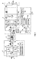
- a stationary frequency generator 2 which generates from a DC voltage source 1, which may be a battery or a capacitor charged to Geichwood, an alternating current i G higher frequency, for example, 100 kHz, which is independent of the amplitude and the phase position of the back voltage u G Amplitude i G has.
- a generator can deliver and record effective and reactive power depending on the phase position of the counter voltage.
- the alternating current i G of the primary winding 3 a of the separation point bridging inductive transformer 3 is supplied.
- the secondary winding 3b of the transformer is connected to an electronic control device 4, which acts as Aktuatorstell Surprise and usually corresponds to a power converter circuit connected.
- the transformer 3 can be a prior art inductive rotary transformer whose primary part is fixed in the pivot point of the movement and whose secondary part is rotatably mounted in the fulcrum.
- the separation point to be bridged runs in this case as an air gap in the interior of the rotary transformer.
- Linear movements are also available for linear movements for bridging a separation point running along the movement path.
- the current i emerging from the secondary winding 3b of the transformer in accordance with its transmission ratio is always impressed in the direction into the capacitive actuator via an electronic actuator positioner 4, separated into positive and negative half oscillations or portions from these half oscillations, in which the amount of the difference u S - u A of a voltage setpoint u S and the current actuator voltage u A from half-oscillation to half-oscillation decreases. If the voltage difference u S -u A has become zero or lies within a tolerance band accepted as zero, the actuator setting device 4 passes the current i to the actuator 5 via a short circuit of the supply lines to the actuator setting device. This short circuit is completely uncritical with impressed current i.
- the capacitive actuator 5 converts the change in length ⁇ s occurring when a charge ⁇ i A dt is applied to a stack 5a of piezoelectric material into a change in angle of a flap 6 via a mechanical transmission 5c.
- the method according to the invention can also be used for adjusting the energy of capacitive actuators, if it is not the task to bridge a separation point with the aid of an inductive transformer.
- the setpoint values u S of the actuator voltage which are generated, for example, in a control system LS as bit-serial data words, must also be supplied to the actuator setting device 4 via the separation point 3c.
- Fig.1 These are transmitted via the separation point by means of an optical or also inductive data transfer device DÜ designed according to the prior art and converted on the movable subsystem by means of a data converter DW into the desired values u S suitable for the actuator setting device.
- the frequency generator 2 is an inverter and consists of a bridge circuit turn-off semiconductor power switch T1-T4, such as MOS field-effect transistors or IGBTs, with a series resonant circuit L G , C G in the bridge diagonal and a coupled to the capacitor C G via the transformer 3 load ,
- T1-T4 semiconductor power switch
- f w the inverter frequency
- the resonant frequency of the series resonant circuit is in the connected to the capacitor transformer 3 a of the opposite voltage u G and thus independent of the connected load current i G with the constant amplitude imprinted.
- û W1 is the fundamental amplitude of the inverter voltage u W , which is maintained at a constant value as the input DC voltage U B fluctuates due to the pulse width modulation contained in the inverter controller 2a.
- the output current amplitude î G of the frequency generator 2 is independent both of the magnitude of the reverse voltage u G and of its phase position relative to the current i G.
- the frequency generator 2 can therefore at constant current î G not only provide active and reactive power via the transformer 3 to the movable secondary part, but also record from this and supply the recorded active power of the DC voltage source U B.
- the bridge circuit of the semiconductor power switches T1 - T4 can, as is known from the general teaching of the power converter technology, be replaced by functionally identical half-bridge circuits with capacitive input voltage divider or transformer center circuits.
- the magnitude of the back voltage u G and its phase position and thus the direction of the energy flow are determined by the actuator 4 connected to the secondary winding 3b of the transformer 3.
- a filter C F , L F At the output of the bridge circuit to the actuator 5 through a filter C F , L F , and in the supply of the higher-frequency alternating current i to the bridge circuit, a filter C L , L L is connected.
- the filter C F , L F serves to limit the high-frequency ripple of the current i A to the actuator 5. Since the actuator voltage u A via the actuator 4 only with a frequency of z. B. is adjusted to a maximum of 500 Hz, the frequency of the current ripple of i A but twice the value of the frequency f w , so for example 200 kHz, the filter is designed so that between the low-frequency actuator voltage u A and the low-frequency voltage component of u ' A on the filter capacitor C F no significant difference exists.
- the voltage difference u ' A - u A which occurs at the filter inductance L F , is the high-frequency voltage ripple, for example 200 kHz.
- the trained as a series resonant circuit and tuned to the frequency f w of the frequency generator 2 and the current i filter C L , L L is a absorption circuit, which represents no resistance to the current i.
- the inductance L L of this filter the voltage differences suddenly occurring during the switching of the power switches S1-S4 between the data transferred from the capacitor C G to the secondary transformer winding 3b voltage u 'G and the low-frequency output voltage u' A ⁇ u A of the actuator control element 4 on.
- a control 4 R is present, whose output signals ⁇ and G / W influence the control 4 ST of the actuator setting device in such a way that the current supplied to the actuator adjusting device i is separated according to positive and negative half oscillations or sections from these oscillations in the Direction is impressed in the capacitive actuator that the amount of the difference u S -u A decreases. If this difference is positive, ie u S > u A , additional charge must be supplied to the actuator.
- the controller is caused to 4 ST via the signal G / W, to control the bridge circuit S1-S4 as a rectifier.
- the signal ⁇ is a measure of the magnitude of the deviation u S -u A and determined as indicated by the Fig. 3 will be explained in more detail, the size of the angle of the half-wave sections.
- the actuator In the case of a negative deviation u S -u A , ie u S ⁇ u A , the actuator is deprived of charge or energy and fed via the actuator control device 4 into the energy transfer circuit through which the higher-frequency current i flows.
- the controller 4 ST now controls, caused by the signal G / W, the bridge circuit S1-S4 as an inverter, wherein the signal ⁇ again determines the size of the angle of the half-wave sections in accordance with the magnitude of the deviation u S -u A.
- the formation of the half-wave sections of the current i takes place by switching the semiconductor switches S1-S4 on and off via the control 4 ST in fine grid steps synchronously with the course of the oscillation.
- the semiconductor switches S1-S4 are switched on only in such time or phase angle ranges in both rectifier and inverter operation, in which the current i already flows via the diode parallel to each switch.
- the current signal of a current transformer SW which detects the higher-frequency current i, via a comparator stage 4 a S1 first phase input E1 of a P ise- L ock- L oop circuit 4 S2 supplied.
- the second phase input E2 is fed by means of an N-stage counter 4 S3 from the output clock f T of the PLL circuit by a factor of 2 N squared signal f TU .
- the PLL circuit 4 S2 sets the frequency of its output clock f T so that the frequency and phase angle deviation between the current signal at the input E1 with the frequency f w and the squat signal with the frequency f TU at the input E2 is zero.
- the N output signals SR of the N-stage counter then form the synchronized with the zero crossings of the AC i switching grid SR.
- N 6
- Fig. 3 illustrate the diagrams a) to e) and the switching states 1 to 6, the setting of the actuator current i A , ie forming the Halbschwingungsabbalde from the current i, for the rectifier and for inverter operation, switching losses when switching the semiconductor switches S1-S4 avoided become.
- Diagram 3a) shows the curve of the voltage u at the AC-side input of the bridge circuit S1-S4 in association with the impressed current i.
- Diagram 3b) shows the associated formation of the current sections from the half-waves of the current i. Voltage and current sections of the inverter operation are characterized by additional puncturing.
- the numbers in the voltage diagram a) indicate time ranges which correspond to the switching states 1 to 6 in the right part of FIG Fig. 3 correspond.
- Diagram c) identifies the conduction regions of the diodes integrated in the switches S1-S4.
- Diagrams d) and e) indicate the possible conduction ranges of the controllable semiconductor switches S1-S4 in the synchronized switching grid SR, namely diagram d) for the rectifier operation and diagram e) for the inverter operation.
- the bordered guide areas indicate the angle or time range in which the associated switches S1-S4 are controlled to the conducting state.
- the guide regions for three settings of the actuator current namely minimum, average and maximum current, are shown.
- the conductive areas have in all operating states such a phase position that the impressed current i passes at its zero crossing either from a diode to the already switched parallel fashion switch or after reloading the Besclienskondensatoren C B continues to flow through the diode of the series-connected switch , As a result, turn-on losses of the controllable semiconductor switches are avoided.
- the current i then recharges the parallel lying Beschariskondensatoren C B and then also flows through the diode of the series-connected switch on.
- the Shutdown must be carried out at an angle ⁇ A so far before the next current zero crossing, that the current i is sufficient to reload in the following on the shutdown gap range ⁇ L parallel to the switches Beschariskondensatoren C B by the amount of the actuator voltage u A.
- the impressed current i flows in the short circuit via the switched-on switches S1 and S2.
- the actuator is shown in simplified form by a DC voltage source with the voltage U A while no current is supplied.
- State 2 begins with the opening of switch S2 at the end of the conductive area of S2 in diagram d).
- the current i now flows in state 2 via the snubber capacitors parallel to the switches S2 and S4. Because of the equality of the capacitors, the current flows through each capacitor i / 2 and only the current of the parallel to S4 capacitor flows through the DC voltage source U A.
- the Umladeschreib 2 is completed and goes into the state 3, when the parallel to S2 capacitor C B on the Voltage U A charged and the capacitor C B lying parallel to S4 is completely discharged.
- Diagram a) shows in association with the current i the associated voltage u at the input of the bridge circuit and diagram b) the corresponding section from a half-oscillation of the current i.
- the switches S1 and S3 are opened with each zero crossing.
- the state 3 goes after the current zero crossing and after the opening of the switch S1 in the state 5, in which now charged to the switch S1 parallel capacitor charged to the voltage U A and parallel to the switch S3 Capacitor be discharged. If the latter is discharged, the parallel diode takes over the current and the switch S3 is closed after the gap region ⁇ L.
- the impressed current i now flows in the region 6 in the short circuit via the switch S3 and the parallel diode and the switch S4.
- the region 6 lying in the negative half-oscillation of the current i corresponds to the region 1 in the positive half-oscillation.
- the conducting regions of all switches in the basic position of the rectifier operation and in the basic position of the inverter operation have the same phase position relative to the impressed current i.
- the basic position of the inverter operation is thus the basic position of the rectifier operation.
- the inverter operation is realized in that now remain the lead areas of the switches S2 and S4 in their normal position S20 and S40 and the phase position of the guide areas of the switches S1 and S3 are moved from their basic position to the right lagging.
- the switch S1 remains closed at the end of the region 3 after the zero crossing of the current i. Area 3, while maintaining the switch positions, transitions with the current zero crossing in area 4 of the inverter operation.
- the energy flow direction changes, the actuator is discharged and the energy is supplied to the AC circuit.
- the transition from the rectifier operation to the inverter operation is carried out by extending the switch state 3 beyond the current zero crossing, without requiring an additional switching operation in the area 4 marked by puncturing.
- the Aktatorstell Stein 4 has, as the diagrams a) to e) and the switching states 1 to 6, in each half of the impressed higher frequency alternating current i successively a phase of the operating state "inverter operation” with the charge and energy transport from the actuator 5, 5a to the AC side , a phase of the operating state “idle” with short-circuited AC input and without changing the charge and energy state of the actuator and a phase of the operating state “rectifier operation” with charge and energy transport from the AC side to the actuator 5, 5a.
- the phase of the "inverter operation” begins automatically with each zero crossing of the current i, if the controllable power semiconductors parallel to the conducting diodes were switched on during the phase of the "rectifier operation" preceding the current zero crossing.
- the phase of the "inverter operation” can be terminated at any time within the current half-cycle by switching off one of the two in the “inverter phase” conductive controllable power semiconductors.
- the Aktuatorstell Surprise then goes into the "idle phase”.
- the phase of the "rectifier operation” is set. This must be done at least at an angle ⁇ A before the following zero crossing of the current i in order to ensure complete transfer of the snubber capacitors C B in the gap region ⁇ L.
- the transition between the phases of the operating states takes place by switch-off processes in which no turn-off losses occur.
- the circuit arrangement according to the FIGS. 1 and 2 allows only the setting of actuator voltages u A of a sign, ie the output line B can be compared to the output line A poled only positive.
- actuator actuators 4 with positive and negative output voltages are required for certain actuators.
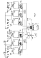
- An actuator setting device 4 which fulfills this requirement is disclosed in US Pat Fig. 5 shown. It differs from the Aktuatorstell Surprise 4 of Fig. 2 in that in the adjusting device 4c in place of the semiconductor switches S1, S2, S3, S4 of the circuit 4a, which only block voltage of one polarity and turn one direction on and off, semiconductor switches can be used which block voltages of both polarities and currents in Both directions can be switched on and off.
- Such bidirectional semiconductor switches consist, for example, as in Fig. 4c and Fig. 5 shown, from a pair of oppositely connected in series controllable semiconductor switch S1P / S3N, S2P / S4N, S3P / S1N, S4P / S2N.
- FIG. 4 illustrated adjusting devices 4a) to 4c) explained.
- Fig. 4a is once again the adjusting device for positive output voltage u ' A of in Fig. 2 shown Aktuatorstelle worn 4 shown.
- the controllable semiconductor switches In order to form a negative output voltage u ' A , the controllable semiconductor switches must relate to the output lines A, B' according to the in Fig. 4b ) are arranged.
- the switches S1-S4 in the arrangement for positive output voltage additionally have the identifier "P" and in the arrangement for negative output voltage additionally the identifier "N".
- the numbers 1-4 indicate in both arrangements semiconductor switches which are driven in phase with respect to the input current i.
- the circuit 4c provides a positive output voltage when denoted by "N"
- Semiconductor switches are permanently switched to the conductive state and the "P" designated semiconductor switch in the on hand of the Figures 2 and 3 be driven described manner.
- the semiconductor switches labeled "P” remain permanently in the conducting state and the semiconductor switches labeled "N” now receive the control signals which, upon generation of a positive output voltage, fuse the semiconductor switches labeled "P” with the semiconductor switches same code be supplied.
- Piezoelectric actuators will be particularly advantageous as Fig. 6 shows equipped with 2 antiphase operated stacks 5a, 5b of piezoelectric material.
- the two piezo stacks 5a and 5b are connected in parallel with respect to an approximately constant bias voltage u AV in series and with respect to a charge transfer voltage u AU applied between the midpoint terminal B and an outer conductor terminal, for example A.
- a double actuator larger travel paths ⁇ s1 + ⁇ s2 and greater actuating forces are achieved than with an actuator which has only one piezo stack.
- the two stacks of a double actuator are largely the same.
- the DC bias voltage can also be generated by a power supply unit formed according to the prior art.
- this power supply must be able to operate at approximately constant output voltage u AV .
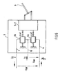
- Fig. 7 has 2 groups of 2 double actuators each.
- Each of the two actuator groups has its own bias setting 4.2 or 4.5. These are supplied with the generally constant bias setpoints VSS2 and VSS5.
- the Aktuatorstell respondeden 4.1 and 4.3 of the first group and the Aktuatorstell respondeden 4.4 and 4.6 of the second group set by the currents i A1 , i A3 and the currents i A4 , i A6 the voltages U AU1 , U AU3 and U AU4 , u AU6 and thus the charges and the length changes of the double actuators according to the voltage setpoints U S1 , U S3 , and U S4 , U S6 , a.
- the frequency generator 2 feeds its output current i G directly into the series-connected primary windings of the input transformers 7.1-7.6.
- potential free and current adaptation to the actuators 4.1 - 4.6 and to the actuators is achieved on their secondary side.
- the outputs of the potential-free actuating devices can therefore be connected to one another and have a common ground potential.
- the input voltages u 1 ' to u 6 ' the control devices 4.1 - 4.6 in Fig. 7 correspond to the input voltage u G ' the adjusting device 4 in Fig. 1 and Fig.
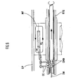
- FIG. 8 Based on FIG. 8 is shown in simplified form, in which way a device described above and the associated method using the device in the region of the rotor shaft GR and the rotor blades BL of a rotary wing aircraft, in particular a helicopter is used.
- Fixedly mounted on board the helicopter are the necessary electronic components, such as the power supply PS, and the frequency generator MFG with the control electronics CI, and also the connection to the flight control STC of the helicopter.
- non-contact coupling devices CD are provided in addition to various bearings BG. These can once in the manner of an optical coupler DÜ (see. Fig. 1 ), as in the case of signal transmission STM of the in the control system LS (see. Fig. 1 ) integrated control electronics CI to the optical waveguide OW is indicated.
- non-contact inductive signal transmissions 3 (cf. Fig. 1 ), which are used, for example, in the energy transmission ETM from the frequency generator MFG to the rotor head electronics RHE.
- the azimuth sensor AZS serves to generate setpoint values for the various actuators as a function of the instantaneous position of the respective rotor blade within one revolution.
- rotor shaft In the area of the rotor shaft further functional units are indicated which are only indirectly related to the invention, such as the mechanical rotor control RCM and the rotor head sensors RHS. From the rotor head electronics RHE further electrical connections lead into the rotor blades BL to the actuators A, which move the rudder flaps FL, and to the sensors S, the position of the rudder flaps FL detect.
- the rudder flaps are exemplary here for various embodiments of aerodynamically effective devices on the rotor blades.
- the rotor electronics RHE thus contains the above-described electronic actuator adjusting device 4 (cf. Fig. 1 . 2 ) and the other necessary for driving and control of the actuators A electronic circuits, such as the data converter DW (see. Fig. 1 ).
- FIG. 9 shows a detailed solution relating to the non-contact inductive energy transmission ETM, which in the FIG. 8 is shown only schematically simplified.
- the rotor shaft RTG designed as a hollow shaft is rotatably mounted.
- the optical waveguide OW for the optical data transmission and coaxially around it the two conductive metal tubes CMW are arranged. Both conductors lead in the direction of the arrow to the right to the rotor head electronics RHE, not shown.
- the two conductive metal tubes CMW are connected via the connecting lines CC to the winding w 2 rotating together with the rotor shaft (corresponding to 3b in FIG. 1 ) electrically connected. Together with the static winding w 1 (corresponding to 3a in FIG. 1 ) forms the rotating winding w 2, the non-contact transformer (corresponding to 3 in FIG. 1 ).
- the leads to the stationary winding w 1 are in the FIG. 9 not explicitly shown.
Landscapes
- Engineering & Computer Science (AREA)
- Power Engineering (AREA)
- Computer Networks & Wireless Communication (AREA)
- General Electrical Machinery Utilizing Piezoelectricity, Electrostriction Or Magnetostriction (AREA)
- Inverter Devices (AREA)
Abstract
Claims (11)
- Dispositif de transmission d'énergie électrique sans contact dans un système, le dispositif comprenant un dispositif de contrôle (2a, 4S1 - 4S3, 4ST, 4R), au moins une partie fixe et une partie mobile entre lesquelles l'énergie doit être transmise, au moins un actionneur (5) à commander et à alimenter en énergie dans la pièce mobile, au moins un dispositif de réglage (4) d'actionneur connecté à l'actionneur (5) à alimenter, un générateur de fréquence (2) comprenant un condensateur à circuit oscillant en série (CG), sur un transformateur inductif (3) pontant un point de sectionnement (3c) entre la pièce fixe et la pièce mobile, dont l'enroulement primaire (3a) est connecté au condensateur à circuit oscillant en série et dont l'enroulement secondaire (3b) disposé sur la pièce mobile est connecté à le au moins un dispositif de réglage d'actionneur (4), caractérisé en ce que le au moins un dispositif de réglage d'actionneur (4) est sous la forme d'un agencement matriciel (4a, 4b, 4c) de semi-conducteurs de puissance commutables (S1,..., S4), en ce que la partie mobile comprend au moins un axe de rotor (GR) et une tête de rotor d'un giravion, les pièces du dispositif de contrôle étant disposées sur la tête de rotor,
et en ce que l'enroulement primaire (3a) est disposé sur la partie fixe d'un palier d'axe de rotor (SP) pour transmettre l'énergie, lequel enroulement primaire correspond à l'enroulement secondaire (3b) disposé sur l'axe du rotor (GR). - Dispositif selon la revendication 1, caractérisé en ce que l'actionneur à commander et à alimenter en énergie est construit sous forme d'actionneur capacitif.
- Dispositif selon la revendication 1 ou 2, caractérisé en ce qu'un ou plusieurs actionneurs capacitifs sont disposés dans au moins une pâle de rotor (BL) du giravion.
- Dispositif selon la revendication 1, caractérisé par les caractéristiques suivantes :a) pour former une tension de sortie (u'A, uA) du dispositif de réglage d'actionneur (4) avec une seule polarité, le conducteur de sortie (A, B') contient des semi-conducteurs de puissance commutables unipolaires (S1, .... S4) en agencement matriciel,b) les semi-conducteurs commutables unipolaires sont mis en oeuvre en se rapportant à la polarité de la tension de sortie, dans laquelle ils captent la tension de sortie (u'A, uA) en tant que tension de blocage et coupent le courant (-IA) du conducteur de sortie positif allant vers une entrée de courant alternatif.
- Dispositif selon la revendication 1, caractérisé en ce que, pour former une tension de sortie (u'A, uA) du dispositif de réglage d'actionneur (4) de polarité changeante, le conducteur de sortie (A, B') comprend des semi-conducteurs de puissance commutables bipolaires en agencement matriciel, qui bloquent des tensions facultativement positives ou négatives et coupent des courants dans les deux sens du flux de courant.
- Dispositif selon l'une des revendications 1, 4 ou 5, caractérisé par les caractéristiques suivantes :- le dispositif de réglage d'actionneur (4) comporte un organe de régulation (4R) et de commande (4ST) d'application de semi-périodes positives ou négatives ou de segments de semi-périodes du courant alternatif (i) d'une fréquence supérieure dans l'actionneur (5, 5a),- l'organe de régulation (4R) est connecté à l'organe de commande (4ST) pour former, par l'intermédiaire d'un signal (ϕ), en fonction du montant de la différence (uS-u'A) entre la valeur de consigne (uS) et la valeur réelle (u'A) de la tension de l'actionneur, des segments de grandeur différente de semi-périodes du courant (i),- l'organe de régulation (4R) est connecté à l'organe de commande (4ST), pour commander, par l'intermédiaire du signal (GNV), en fonction du signe de la différence (uS-u'A) entre la valeur de consigne (uS) et la valeur réelle (u'A) de la tension d'actionneur, les semi-conducteurs de puissance (S1, S2, S3, S4) de manière à ce qu'en cas de signe négatif de la différence (uS-u'A), d'une semi-période à une autre semi-période, une charge ou de l'énergie successive pour l'actionneur est coupée (5, 5a) ou qu'en cas de signe positif de la différence (uS-u'A), d'une semi-période à une autre semi-période, une charge ou de l'énergie successive est alimentée à l'actionneur (5, 5a).
- Dispositif selon l'une des revendications 1 et 4 à 6, caractérisé par les caractéristiques suivantes :a) l'organe de commande (4ST) d'application de semi-périodes ou de segments de semi-périodes du courant alternatif (i) dans l'actionneur est connecté à des dispositifs (4S1, 4S2, 4S3) permettant de générer des signaux (SR) d'une grille de commutation synchronisée au courant alternatif (i),b) l'organe de commande (4ST) comprend des moyens logiques, qui forment à partir des signaux (SR) de la grille de commutation des signaux de plage conductrice (S10, S30) et (S20, S40) à l'état initial des paires de commutateurs à semi-conducteurs disposées en série (S1, S3) et (S2, S4).c) l'organe de commande (4ST) comprend des moyens de décalage avancé des plages conductrices de la paire de commutateurs (S2, S4) vis-à-vis de l'état initial (S20, S40), en fonctionnement de convertisseur alternatif-continu, et comprend des moyens de décalage de retard de phase des plages conductrices de la paire de commutateurs (S1, S3) vis-à-vis de l'état initial (S10, S30), en fonctionnement de convertisseur continu-alternatif,d) l'organe de commande (4ST) est connecté à l'organe de régulation (4R) pour acheminer un signal (G/W) de réglage du sens de décalage et un signal (ϕ) de réglage de la grandeur du décalage.
- Dispositif selon la revendication 1 ou 8, caractérisé en ce qu'un détecteur d'azimut (AZS) est disposé dans le domaine de l'axe du rotor, dont la sortie est connectée au dispositif de contrôle.
- Dispositif selon l'une des revendications 2 ou 81, caractérisé en ce qu'au moins un détecteur permettant de détecter la position d'un organe aérodynamiquement actif actionné par l'actionneur capacitif est disposé dans le domaine de la pâle de rotor, dont la sortie est connectée au dispositif de contrôle.
- Dispositif selon l'une des revendications 1, 8 ou 9, caractérisé en ce que le dispositif de réglage d'actionneur (4) et une électronique de commande correspondante (RHE) sont disposés dans la tête de rotor et sont connectés au transformateur par l'intermédiaire des lignes disposées dans l'axe du rotor.
- Procédé de transmission d'énergie électrique sans contact dans un système, qui comprend au moins une pièce fixe et une pièce mobile, moyennant quoi le dispositif selon l'une des revendications 1, 4 à 7 est implanté dans le système, lequel procédé comprenant les étapes suivantes exécutées au moyen du dispositif implanté :- dans le creux fixe, le générateur de fréquence (2) génère à partir d'une tension continue (1) un courant alternatif (IG) de fréquence plus haute ayant une amplitude indépendante de la position de phase et de l'amplitude de la tension inverse (UG),- le courant alternatif (IG) est amené à l'enroulement primaire (3a) du transformateur (3) inductif pontant le point de sectionnement,- le courant alternatif (i) de fréquence plus haute partant de l'enroulement secondaire (3b) sur la pièce mobile est séparé au moyen du dispositif de réglage d'actionneur (4) selon les semi-périodes positives et négatives ou les segments de ces semi-périodes et est appliqué toujours dans un actionneur (5), dans une certaine direction, de telle sorte que dans chaque semi-période, une modification en longueur (Δs) de l'actionneur se produit dans la direction souhaitée.
Applications Claiming Priority (3)
| Application Number | Priority Date | Filing Date | Title |
|---|---|---|---|
| DE10301978 | 2003-01-20 | ||
| DE2003101978 DE10301978A1 (de) | 2003-01-20 | 2003-01-20 | Vorrichtung und Verfahren zum Übertragen und Bereitstellen der Energie kapazitiver Aktuatoren |
| PCT/EP2003/014214 WO2004066481A2 (fr) | 2003-01-20 | 2003-12-13 | Dispositif et procede permettant de transmettre et de mettre a disposition l'energie d'actionneurs capacitifs |
Publications (2)
| Publication Number | Publication Date |
|---|---|
| EP1586153A2 EP1586153A2 (fr) | 2005-10-19 |
| EP1586153B1 true EP1586153B1 (fr) | 2011-02-09 |
Family
ID=32667677
Family Applications (1)
| Application Number | Title | Priority Date | Filing Date |
|---|---|---|---|
| EP20030799479 Expired - Lifetime EP1586153B1 (fr) | 2003-01-20 | 2003-12-13 | Dispositif et procede permettant de transmettre et de mettre a disposition l'energie d'actionneurs capacitifs |
Country Status (5)
| Country | Link |
|---|---|
| US (1) | US7579715B2 (fr) |
| EP (1) | EP1586153B1 (fr) |
| AU (1) | AU2003299308A1 (fr) |
| DE (2) | DE10301978A1 (fr) |
| WO (1) | WO2004066481A2 (fr) |
Families Citing this family (30)
| Publication number | Priority date | Publication date | Assignee | Title |
|---|---|---|---|---|
| DE102005003850B4 (de) * | 2005-01-27 | 2009-03-19 | Festo Ag & Co. Kg | Fluidtechnische Anordnung |
| DE102005047551A1 (de) * | 2005-09-30 | 2007-04-12 | Siemens Ag | Erregereinrichtung für eine elektrische Maschine |
| DE102007050265B4 (de) * | 2007-10-18 | 2020-12-17 | Sew-Eurodrive Gmbh & Co Kg | System mit relativ zu einem Primärleitersystem bewegbar angeordnetem Verbraucher |
| WO2009089253A1 (fr) | 2008-01-07 | 2009-07-16 | Access Business Group International Llc | Alimentation électrique inductrice avec commande de cycle de marche |
| US8203294B2 (en) * | 2008-11-25 | 2012-06-19 | GE Aviations Systems LLC | Electric energy storage integrated within or proximate to electrically driven flight control actuators |
| US8923015B2 (en) * | 2008-11-26 | 2014-12-30 | Auckland Uniservices Limited | Primary-side power control for inductive power transfer |
| US8331196B2 (en) | 2009-04-14 | 2012-12-11 | Covaris, Inc. | System and method for controlling an acoustic transducer |
| US8750007B2 (en) * | 2010-03-23 | 2014-06-10 | Qualcomm Incorporated | Power conversion |
| US10343535B2 (en) | 2010-04-08 | 2019-07-09 | Witricity Corporation | Wireless power antenna alignment adjustment system for vehicles |
| JP5928865B2 (ja) * | 2010-11-18 | 2016-06-01 | 富士電機株式会社 | 非接触給電装置の制御方法 |
| WO2012101905A1 (fr) * | 2011-01-26 | 2012-08-02 | 株式会社村田製作所 | Dispositif d'alimentation à découpage |
| WO2012107077A1 (fr) * | 2011-02-08 | 2012-08-16 | Siemens Aktiengesellschaft | Système de distribution d'énergie avec convertisseur matriciel multiphase et procédé permettant de le faire fonctionner |
| DE102012013938A1 (de) * | 2011-08-02 | 2013-02-07 | Sew-Eurodrive Gmbh & Co. Kg | Elektronisches Gerät, insbesondere Übertragerkopf, und System zur kontaktlosen Energieübertragung |
| US9257936B2 (en) * | 2011-08-04 | 2016-02-09 | President And Fellows Of Harvard College | System and method for efficient drive of capacitive actuators with voltage amplification |
| US8422249B2 (en) * | 2011-08-25 | 2013-04-16 | Direct Grid Technologies, LLC | Apparatus for a microinverter particularly suited for use in solar power installations |
| FR2990809B1 (fr) * | 2012-05-21 | 2017-04-14 | Hispano-Suiza | Systeme d'alimentation en energie electrique comprenant une machine asynchrone et moteur de propulsion equipe d'un tel systeme d'alimentation en energie electrique |
| EP2733839B1 (fr) | 2012-11-14 | 2017-01-04 | AIRBUS HELICOPTERS DEUTSCHLAND GmbH | Circuit électrique avec un amplificateur de puissance pour actionneurs piézoélectriques antagonistes |
| EP2743179B1 (fr) | 2012-12-17 | 2016-06-01 | Airbus Defence and Space GmbH | Agencement d'actionneur et agencement de surface de commande, notamment pour un aéronef |
| JP6047442B2 (ja) | 2013-03-29 | 2016-12-21 | 富士電機株式会社 | 給電装置 |
| JP6124336B2 (ja) | 2013-06-12 | 2017-05-10 | 東海旅客鉄道株式会社 | 給電装置 |
| JP6129669B2 (ja) * | 2013-07-18 | 2017-05-17 | 東海旅客鉄道株式会社 | 給電装置 |
| US20150311724A1 (en) * | 2014-03-31 | 2015-10-29 | Evatran Group, Inc. | Ac inductive power transfer system |
| DE102014207854A1 (de) * | 2014-04-25 | 2015-10-29 | Robert Bosch Gmbh | Übertragungssystem, Verfahren und Fahrzeuganordnung |
| DE102014110003A1 (de) * | 2014-07-16 | 2016-01-21 | Vermes Microdispensing GmbH | Phasenabschnittsteuerung von Piezoaktoren |
| EP3204997A4 (fr) | 2014-10-08 | 2018-02-14 | PowerbyProxi Limited | Onduleur pour émetteur de puissance inductive |
| CN107431381A (zh) * | 2015-03-13 | 2017-12-01 | 鲍尔拜普罗克西有限公司 | 电感式功率接收器 |
| US10193229B2 (en) * | 2015-09-10 | 2019-01-29 | Cpg Technologies, Llc | Magnetic coils having cores with high magnetic permeability |
| FR3056555B1 (fr) * | 2016-09-29 | 2018-12-07 | Safran Helicopter Engines | Systeme propulsif hybride pour aeronef a voilure tournante multirotor comprenant des moyens ameliores de conversion dc/ac |
| GB2578433B (en) * | 2018-10-25 | 2022-08-17 | Safran Electrical & Power | Electric machine control |
| CN114400647B (zh) * | 2021-12-23 | 2024-02-13 | 智寰(北京)氢能科技有限公司 | 一种耐高频电压纹波的电压闪变抑制装置 |
Family Cites Families (23)
| Publication number | Priority date | Publication date | Assignee | Title |
|---|---|---|---|---|
| GB1291271A (en) * | 1968-10-07 | 1972-10-04 | Sud Aviation | Improvements in or relating to power transmitting mechanisms, and applications thereof, notably to helicopters |
| US4953068A (en) | 1989-11-08 | 1990-08-28 | Unisys Corporation | Full bridge power converter with multiple zero voltage resonant transition switching |
| US5709291A (en) | 1992-05-22 | 1998-01-20 | Daifuku Co., Ltd. | Device for contactless power supply to moving body |
| US5637973A (en) * | 1992-06-18 | 1997-06-10 | Kabushiki Kaisha Yaskawa Denki | Noncontacting electric power transfer apparatus, noncontacting signal transfer apparatus, split-type mechanical apparatus employing these transfer apparatus and a control method for controlling same |
| JP3358244B2 (ja) * | 1993-08-04 | 2002-12-16 | 株式会社デンソー | 圧電アクチュエータ用駆動装置 |
| GB2293522B (en) | 1994-09-02 | 1999-01-20 | Ultra Electronics Ltd | Rotary apparatus |
| DE4446779C2 (de) * | 1994-12-24 | 1996-12-19 | Daimler Benz Ag | Anordnung zur berührungslosen induktiven Übertragung elektrischer Leistung |
| JP3085989B2 (ja) * | 1996-06-24 | 2000-09-11 | シーメンス アクチエンゲゼルシヤフト | 測定電気量及び/又は電気エネルギーを回転子と固定子との間で無接触で誘導的に伝送する装置 |
| DE19709717C1 (de) * | 1997-03-10 | 1998-09-24 | Siemens Ag | Vorrichtung und Verfahren zum Ansteuern wenigstens eines kapazitiven Stellgliedes |
| US6032546A (en) * | 1997-07-21 | 2000-03-07 | Stone; Neil | System for transferring electrical power between non-contacting elements in relative motion |
| DE19735624C1 (de) * | 1997-08-18 | 1998-12-10 | Daimler Benz Ag | Verfahren und Anordnung zur induktiven Übertragung elektrischer Leistung auf mehrere bewegte Verbraucher |
| US6232775B1 (en) * | 1997-12-26 | 2001-05-15 | Alps Electric Co., Ltd | Magneto-impedance element, and azimuth sensor, autocanceler and magnetic head using the same |
| DE19838137A1 (de) * | 1998-08-21 | 2000-03-02 | Implex Hear Tech Ag | Vorrichtung und Verfahren zum Laden von wiederaufladbaren Akkumulatoren von Implantaten |
| GB2346744A (en) * | 1999-02-11 | 2000-08-16 | Alstom Uk Ltd | Heavy duty isolating converter |
| DE19927087A1 (de) | 1999-06-15 | 2000-12-21 | Bosch Gmbh Robert | Vorrichtung zum Laden und Entladen mehrerer piezoelektrischer Elemente |
| DE19927190A1 (de) * | 1999-06-15 | 2000-12-21 | Bosch Gmbh Robert | Verfahren und Vorrichtung zum Laden und Entladen eines piezoelektrischen Elements |
| US6231013B1 (en) * | 1999-06-16 | 2001-05-15 | Daimlerchrysler Ag | Airfoil member with a piezoelectrically actuated servo-flap |
| US6301128B1 (en) | 2000-02-09 | 2001-10-09 | Delta Electronics, Inc. | Contactless electrical energy transmission system |
| WO2002064426A1 (fr) * | 2001-02-14 | 2002-08-22 | Airscooter Corporation | Aeronef ultraleger a rotors coaxiaux |
| DE10116479C2 (de) * | 2001-04-03 | 2003-12-11 | Eurocopter Deutschland | Verfahren und Regeleinrichtung zur Verstellung einer im Rotorblatt eines Hubschraubers schwenkbar gelagerten Klappe |
| FR2837784B1 (fr) * | 2002-03-28 | 2004-05-28 | Eurocopter France | Rotor de giravion a entrainement homocinetique avec differentiel de partage de couple |
| US6845941B2 (en) * | 2002-06-04 | 2005-01-25 | Bret D. Pica | Rotary/fixed wing aircraft |
| US6934167B2 (en) * | 2003-05-01 | 2005-08-23 | Delta Electronics, Inc. | Contactless electrical energy transmission system having a primary side current feedback control and soft-switched secondary side rectifier |
-
2003
- 2003-01-20 DE DE2003101978 patent/DE10301978A1/de not_active Withdrawn
- 2003-12-13 EP EP20030799479 patent/EP1586153B1/fr not_active Expired - Lifetime
- 2003-12-13 DE DE50313468T patent/DE50313468D1/de not_active Expired - Lifetime
- 2003-12-13 AU AU2003299308A patent/AU2003299308A1/en not_active Abandoned
- 2003-12-13 WO PCT/EP2003/014214 patent/WO2004066481A2/fr not_active Ceased
- 2003-12-13 US US10/542,638 patent/US7579715B2/en not_active Expired - Fee Related
Also Published As
| Publication number | Publication date |
|---|---|
| WO2004066481A8 (fr) | 2004-12-16 |
| AU2003299308A8 (en) | 2004-08-13 |
| US7579715B2 (en) | 2009-08-25 |
| EP1586153A2 (fr) | 2005-10-19 |
| WO2004066481A3 (fr) | 2005-01-27 |
| AU2003299308A1 (en) | 2004-08-13 |
| DE10301978A1 (de) | 2004-08-05 |
| DE50313468D1 (de) | 2011-03-24 |
| US20060267523A1 (en) | 2006-11-30 |
| WO2004066481A2 (fr) | 2004-08-05 |
Similar Documents
| Publication | Publication Date | Title |
|---|---|---|
| EP1586153B1 (fr) | Dispositif et procede permettant de transmettre et de mettre a disposition l'energie d'actionneurs capacitifs | |
| DE19630983C1 (de) | Wandler | |
| AT516214B1 (de) | DC/DC-Wandler | |
| EP2425513B1 (fr) | Module avec un dispositif de stockage d'énergie électrique supplémentaire pour un convertisseur multi-niveaux modulaire | |
| DE112013007233T5 (de) | DC/DC-Umsetzer | |
| EP2577844B1 (fr) | Réseau de bord pour un véhicule automobile, véhicule automobile et procédé pour faire fonctionner un réseau de bord | |
| DE2932549C2 (de) | Stromversorgungssystem für Langstator-Linearmotor | |
| DE102007029388A1 (de) | Eigenstromversorgung für Stromrichterschaltertreiber | |
| DE112017003632T5 (de) | Dc/dc-umrichter | |
| WO2015014866A1 (fr) | Convertisseur-élévateur, onduleur correspondant et procédé de fonctionnement | |
| WO2012010288A2 (fr) | Procédé pour chauffer un système de batteries | |
| DE112015006096T5 (de) | Dc/dc-umsetzer | |
| DE102010052272A1 (de) | Verstellvorrichtung zum Verstellen eines Rotorblattanstellwinkels einer Windenergieanlage | |
| EP1976108A2 (fr) | Convertisseur, en particulier pour une turbine à ions | |
| EP2709257A2 (fr) | Circuit de convertisseur de courant et procédé de commande du circuit de convertisseur de courant | |
| EP3332466B1 (fr) | Onduleur inverseur de polarité et avec capacité de puissance réactive ainsi que procédé d'inversion de polarité | |
| WO2014060302A2 (fr) | Onduleur avec un circuit d'adaptation pour des hautes tensions d'entrée continues variables et emploi du circuit d'adaptation | |
| DE102007016039A1 (de) | Vorrichtung und Verfahren zur Ansteuerung einer induktiven Last | |
| WO2016012465A1 (fr) | Circuit pour onduleur multipoints npc comprenant un réseau de décharge | |
| DE102017213145A1 (de) | Verfahren zum Betreiben eines DC-DC-Wandlers | |
| EP3915186A1 (fr) | Convertisseur continu-continu comprenant un circuit de pont pour la mise hors tension ainsi que procédé correspondant | |
| DE102010021402A1 (de) | Bordnetz für ein Kraftfahrzeug, Kraftfahrzeug und Verfahren zum Betreiben eines elektrischen Verbrauchers | |
| DE102014012028A1 (de) | Vorrichtung und ein Verfahren zum Laden oder Entladen eines elektrischen Energiespeichers mit beliebigen Betriebsspannungen | |
| WO2002049197A2 (fr) | Procede d'alimentation d'une charge inductive au moyen d'onduleurs montes en parallele, a commutation progressive | |
| DE102015208568B4 (de) | Bordnetz-Schaltmodul, Bordnetzunterstützungseinrichtung und Bordnetzzweig |
Legal Events
| Date | Code | Title | Description |
|---|---|---|---|
| PUAI | Public reference made under article 153(3) epc to a published international application that has entered the european phase |
Free format text: ORIGINAL CODE: 0009012 |
|
| 17P | Request for examination filed |
Effective date: 20050628 |
|
| AK | Designated contracting states |
Kind code of ref document: A2 Designated state(s): AT BE BG CH CY CZ DE DK EE ES FI FR GB GR HU IE IT LI LU MC NL PT RO SE SI SK TR |
|
| AX | Request for extension of the european patent |
Extension state: AL LT LV MK |
|
| DAX | Request for extension of the european patent (deleted) | ||
| RBV | Designated contracting states (corrected) |
Designated state(s): DE GB IT |
|
| RIN1 | Information on inventor provided before grant (corrected) |
Inventor name: REINERS DIETER Inventor name: SEELIG, ANTON Inventor name: LUTHER JUERGEN |
|
| 17Q | First examination report despatched |
Effective date: 20100430 |
|
| R17C | First examination report despatched (corrected) |
Effective date: 20100525 |
|
| RIC1 | Information provided on ipc code assigned before grant |
Ipc: H02J 5/00 20060101AFI20100831BHEP Ipc: H02M 3/335 20060101ALI20100831BHEP Ipc: H01L 41/04 20060101ALN20100831BHEP Ipc: B64C 27/00 20060101ALN20100831BHEP |
|
| GRAP | Despatch of communication of intention to grant a patent |
Free format text: ORIGINAL CODE: EPIDOSNIGR1 |
|
| GRAS | Grant fee paid |
Free format text: ORIGINAL CODE: EPIDOSNIGR3 |
|
| GRAA | (expected) grant |
Free format text: ORIGINAL CODE: 0009210 |
|
| AK | Designated contracting states |
Kind code of ref document: B1 Designated state(s): DE GB IT |
|
| REG | Reference to a national code |
Ref country code: GB Ref legal event code: FG4D Free format text: NOT ENGLISH |
|
| REF | Corresponds to: |
Ref document number: 50313468 Country of ref document: DE Date of ref document: 20110324 Kind code of ref document: P |
|
| REG | Reference to a national code |
Ref country code: DE Ref legal event code: R096 Ref document number: 50313468 Country of ref document: DE Effective date: 20110324 |
|
| PLBE | No opposition filed within time limit |
Free format text: ORIGINAL CODE: 0009261 |
|
| STAA | Information on the status of an ep patent application or granted ep patent |
Free format text: STATUS: NO OPPOSITION FILED WITHIN TIME LIMIT |
|
| 26N | No opposition filed |
Effective date: 20111110 |
|
| REG | Reference to a national code |
Ref country code: DE Ref legal event code: R097 Ref document number: 50313468 Country of ref document: DE Effective date: 20111110 |
|
| PGFP | Annual fee paid to national office [announced via postgrant information from national office to epo] |
Ref country code: DE Payment date: 20131121 Year of fee payment: 11 Ref country code: GB Payment date: 20131125 Year of fee payment: 11 |
|
| REG | Reference to a national code |
Ref country code: DE Ref legal event code: R082 Ref document number: 50313468 Country of ref document: DE Representative=s name: GPI & ASSOCIES, FR |
|
| REG | Reference to a national code |
Ref country code: DE Ref legal event code: R081 Ref document number: 50313468 Country of ref document: DE Owner name: AIRBUS HELICOPTERS DEUTSCHLAND GMBH, DE Free format text: FORMER OWNER: EUROCOPTER DEUTSCHLAND GMBH, 86609 DONAUWOERTH, DE Effective date: 20150112 Ref country code: DE Ref legal event code: R082 Ref document number: 50313468 Country of ref document: DE Representative=s name: GPI & ASSOCIES, FR Effective date: 20150112 |
|
| REG | Reference to a national code |
Ref country code: DE Ref legal event code: R119 Ref document number: 50313468 Country of ref document: DE |
|
| GBPC | Gb: european patent ceased through non-payment of renewal fee |
Effective date: 20141213 |
|
| PG25 | Lapsed in a contracting state [announced via postgrant information from national office to epo] |
Ref country code: GB Free format text: LAPSE BECAUSE OF NON-PAYMENT OF DUE FEES Effective date: 20141213 Ref country code: DE Free format text: LAPSE BECAUSE OF NON-PAYMENT OF DUE FEES Effective date: 20150701 |
|
| PGFP | Annual fee paid to national office [announced via postgrant information from national office to epo] |
Ref country code: IT Payment date: 20171221 Year of fee payment: 15 |
|
| PG25 | Lapsed in a contracting state [announced via postgrant information from national office to epo] |
Ref country code: IT Free format text: LAPSE BECAUSE OF NON-PAYMENT OF DUE FEES Effective date: 20181213 |